

Philips PBSS5350Z Technical data
查询PBSS5350Z供应商
DISCRETE SEMICONDUCTORS
DATA SH EET
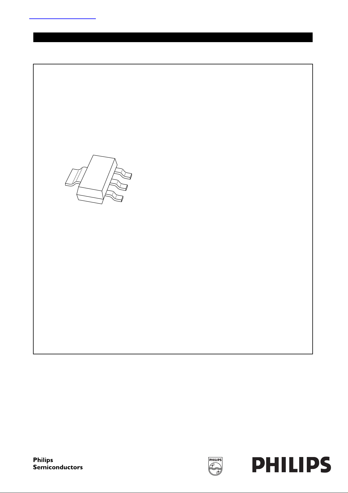
handbook, halfpage
M3D087
PBSS5350Z
50 V low V
Product specification
Supersedes data of 2003 Jan 20
CEsat
PNP transistor
2003 May 13

Philips Semiconductors Product specification
50 V low V
CEsat
PNP transistor
FEATURES
• Low collector-emitter saturation voltage
• High collector current capability: IC and I
• High collector current gain (hFE) at high I
CM
C
• Higher efficiency leading to less heat generation
• Reduced PCB area requirements compared to DPAK.
APPLICATIONS
• Power management
– DC/DC converters
– Supply line switching
– Battery charger
– Linear voltage regulation (LDO).
• Peripheral drivers
– Driver in lowsupply voltage applications, e.g. lamps,
LEDs
– Inductive load driver, e.g. relays, buzzers, motors.
PBSS5350Z
QUICK REFERENCE DATA
SYMBOL PARAMETER MAX. UNIT
V
CEO
I
C
I
CM
R
CEsat
PINNING
PIN DESCRIPTION
1 base
2 collector
3 emitter
4 collector
handbook, halfpage
collector-emitter voltage −50 V
collector current (DC) −3A
peak collector current −5A
equivalent on-resistance <150 mΩ
4
2, 4
DESCRIPTION
PNP low V
transistor in a SOT223 plastic package.
CEsat
NPN complement: PBSS4350Z.
MARKING
TYPE NUMBER MARKING CODE
PBSS5350Z PB5350
1
123
Top view
MAM288
3
Fig.1 Simplified outline (SOT223) and symbol.
2003 May 13 2
Philips Semiconductors Product specification
50 V low V
CEsat
PNP transistor
PBSS5350Z
LIMITING VALUES
In accordance with the Absolute Maximum Rating System (IEC 60134).
SYMBOL PARAMETER CONDITIONS MIN. MAX. UNIT
V
CBO
V
CEO
V
EBO
I
C
I
CM
I
BM
P
tot
T
stg
T
j
T
amb
collector-base voltage open emitter −−60 V
collector-emitter voltage open base −−50 V
emitter-base voltage open collector −−6V
collector current (DC) −−3A
peak collector current −−5A
peak base current −−1A
total power dissipation T
≤ 25 °C; notes 1 and 3 − 1.35 W
amb
T
≤ 25 °C; notes 2 and 3 − 2W
amb
storage temperature −65 +150 °C
junction temperature − 150 °C
operating ambient temperature −65 +150 °C
Notes
1. Device mounted on a printed-circuit board; single sided copper; tinplated; mounting pad for collector 1 cm2.
2. Device mounted on a printed-circuit board; single sided copper; tinplated; mounting pad for collector 6 cm2.
3. For other mounting conditions see
Handbook”
.
“Thermal considerations for SOT223 in the General Part of associated
THERMAL CHARACTERISTICS
SYMBOL PARAMETER CONDITIONS VALUE UNIT
R
th j-a
thermal resistance from junction to ambient in free air; notes 1 and 3 92 K/W
in free air; notes 2 and 3 62.5 K/W
Notes
1. Device mounted on a printed-circuit board; single sided copper; tinplated; mounting pad for collector 1 cm.
2. Device mounted on a printed-circuit board; single sided copper; tinplated; mounting pad for collector 6 cm2.
3. For other mounting conditions see
Handbook”
.
“Thermal considerations for SOT223 in the General Part of associated
2003 May 13 3

Philips Semiconductors Product specification
50 V low V
CEsat
PNP transistor
PBSS5350Z
CHARACTERISTICS
T
=25°C unless otherwise specified.
amb
SYMBOL PARAMETER CONDITIONS MIN. TYP. MAX. UNIT
I
CBO
I
EBO
h
FE
V
CEsat
R
CEsat
V
BEsat
collector-base cut-off current VCB= −50 V; IE=0 −−−100 nA
V
= −50 V; IE= 0; Tj= 150 °C −−−50 µA
CB
emitter-base cut-off current VEB= −5 V; IC=0 −−−100 nA
DC current gain VCE= −2V;
I
=−500 mA 200 −−
C
=−1 A; note 1 200 −−
I
C
I
=−2 A; note 1 100 −−
C
collector-emitter saturation
voltage
IC= −500 mA; IB= −50 mA −−−100 mV
= −1 A; IB= −50 mA −−−180 mV
I
C
I
= −2 A; IB= −200 mA; note 1 −−−300 mV
C
equivalent on-resistance IC= −2 A; IB= −200 mA; note 1 − 120 <150 mΩ
base-emitter saturation
IC= −2 A; IB= −200 mA; note 1 −−−1.2 V
voltage
V
f
T
BEon
base-emitter turn-on voltage VCE= −2 V; IC= −1 A; note 1 −−−1.1 V
transition frequency IC= −100 mA; VCE= −5V;
100 −−MHz
f = 100 MHz
C
c
collector capacitance VCB= −10 V; IE=Ie= 0; f = 1 MHz −−40 pF
Note
1. Pulse test: t
≤ 300 µs; δ≤0.02.
p
2003 May 13 4
 Loading...