

Philips PBSS5320T Technical data
查询PBSS5320T供应商
DISCRETE SEMICONDUCTORS
DATA SH EET
PBSS5320T
20 V, 3 A
PNP low V
Product specification
Supersedes data of 2002 Aug 08
CEsat
(BISS) transistor
2004 Jan 15
Philips Semiconductors Product specification
20 V, 3 A
PNP low V
CEsat
FEATURES
• Low collector-emitter saturation voltage V
corresponding low R
• High collector current capability
• High collector current gain
• Improved efficiency due to reduced heat generation.
APPLICATIONS
• Power management applications
• Low and medium power DC/DC convertors
• Supply line switching
• Battery chargers
• Linear voltage regulation with low voltage drop-out
(LDO).
DESCRIPTION
(BISS) transistor
CEsat
CEsat
and
PBSS5320T
QUICK REFERENCE DATA
SYMBOL PARAMETER MAX. UNIT
V
CEO
I
C
I
CRP
R
CEsat
PINNING
PIN DESCRIPTION
1 base
2 emitter
3 collector
collector-emitter voltage −20 V
collector current (DC) −2A
repetitive peak collector
−3A
current
equivalent on-resistance 105 mΩ
PNP low V
NPN complement: PBSS4320T.
MARKING
TYPE NUMBER MARKING CODE
PBSS5320T ZH∗
Note
transistor in a SOT23 plastic package.
CEsat
(1)
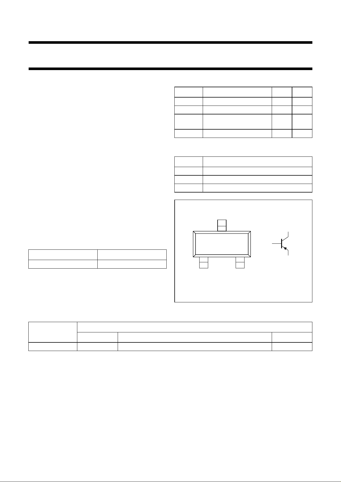
handbook, halfpage
Top view
3
1
21
MAM256
3
2
1. ∗ = p: Made in Hong Kong.
∗ = t: Made in Malaysia.
Fig.1 Simplified outline (SOT23) and symbol.
∗ = W: Made in China.
ORDERING INFORMATION
PACKAGE
TYPE NUMBER
NAME DESCRIPTION VERSION
PBSS5320T − plastic surface mounted package; 3 leads SOT23
2004 Jan 15 2
Philips Semiconductors Product specification
20 V, 3 A
PBSS5320T
PNP low V
LIMITING VALUES
In accordance with the Absolute Maximum Rating System (IEC 60134).
SYMBOL PARAMETER CONDITIONS MIN. MAX. UNIT
V
V
V
I
C
I
CRP
I
CM
I
B
P
T
T
T
CBO
CEO
EBO
tot
stg
j
amb
collector-base voltage open emitter −−20 V
collector-emitter voltage open base −−20 V
emitter-base voltage open collector −−5V
collector current (DC) −−2A
repetitive peak collector current note 1 −−3A
peak collector current single peak −−5A
base current (DC) −−0.5 A
total power dissipation T
storage temperature −65 +150 °C
junction temperature − 150 °C
operating ambient temperature −65 +150 °C
(BISS) transistor
CEsat
≤ 25 °C; note 2 − 300 mW
amb
T
≤ 25 °C; note 3 − 480 mW
amb
T
≤ 25 °C; note 4 − 540 mW
amb
T
≤ 25 °C; notes 1 and 2 − 1.2 W
amb
Notes
1. Operated under pulsed conditions: pulse width tp≤ 100 ms; duty cycle δ≤0.25.
2. Device mounted on a printed-circuit board; single sided copper; tin plated; standard footprint.
3. Device mounted on a printed-circuit board; single sided copper; tin plated; mounting pad for collector 1 cm2.
4. Device mounted on a printed-circuit board; single sided copper; tin plated; mounting pad for collector 6 cm2.
THERMAL CHARACTERISTICS
SYMBOL PARAMETER CONDITIONS VALUE UNIT
R
th(j-a)
thermal resistance from junction to
ambient
in free air; note 1 417 K/W
in free air; note 2 260 K/W
in free air; note 3 230 K/W
in free air; notes 1 and 4 104 K/W
Notes
1. Device mounted on a printed-circuit board; single sided copper; tin plated; standard footprint.
2. Device mounted on a printed-circuit board; single sided copper; tin plated; mounting pad for collector 1 cm2.
3. Device mounted on a printed-circuit board; single sided copper; tin plated; mounting pad for collector 6 cm2.
4. Operated under pulsed conditions: pulse width tp≤ 100 ms; duty cycle δ≤0.25.
2004 Jan 15 3
 Loading...