

Philips PBSS5240Y Technical data

查询PBSS5240Y供应商
DISCRETE SEMICONDUCTORS
DATA SH EET
ge
MBD128
PBSS5240Y
40 V low V
Product specification
Supersedes data of 2001 Oct 24
CEsat
PNP transistor
2002 Feb 28
Philips Semiconductors Product specification
40 V low V
CEsat
PNP transistor
FEATURES
• Low collector-emitter saturation voltage
• High current capability
• Improved device reliability due to reduced heat
generation
• Replacement for SOT89/SOT223 standard packaged
transistors due to enhanced performance.
APPLICATIONS
• Supply line switching circuits
• Battery management applications
• DC/DC converter applications
• Strobe flash units
• Heavydutybatterypoweredequipment(motorandlamp
drivers).
DESCRIPTION
PBSS5240Y
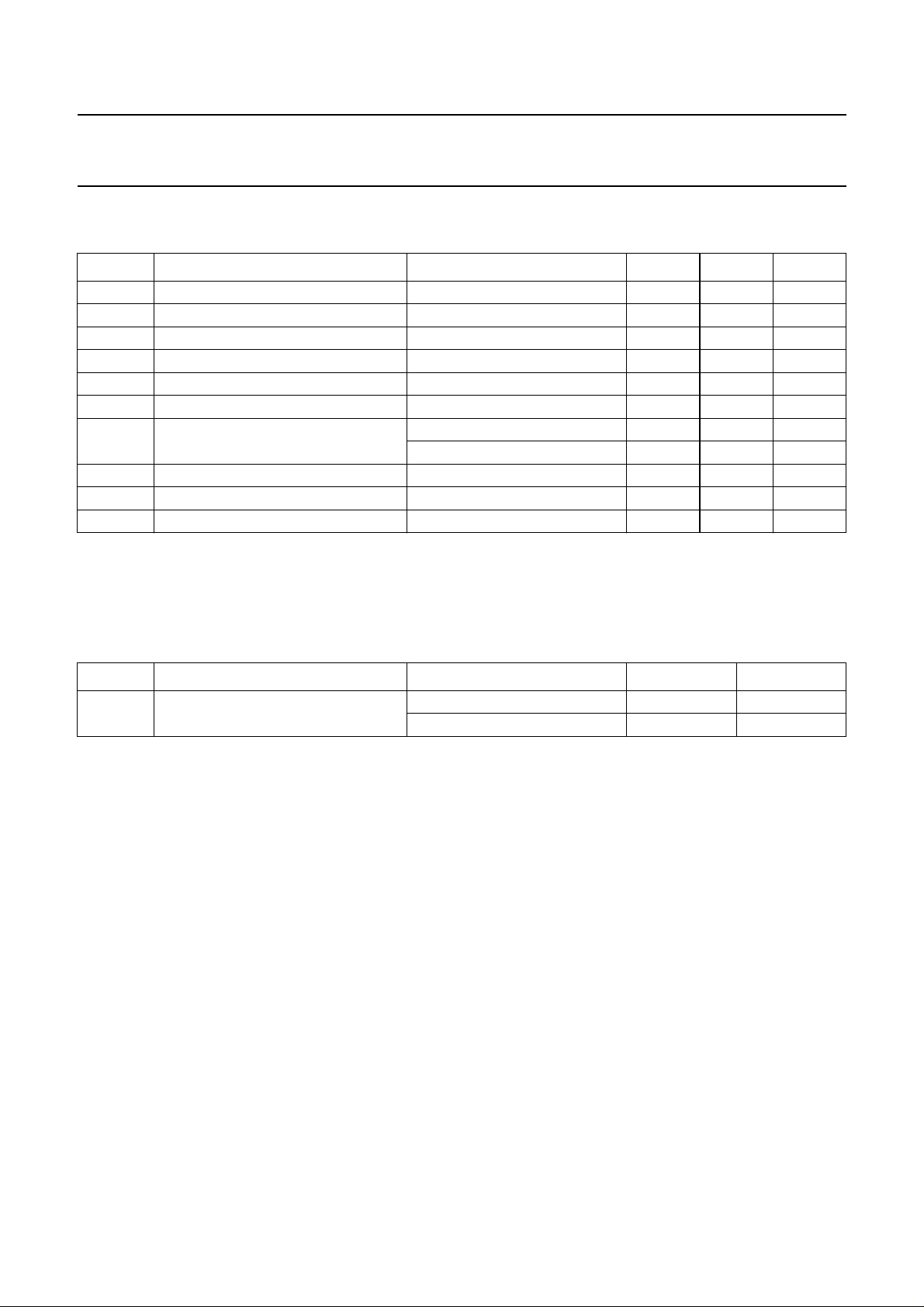
QUICK REFERENCE DATA
SYMBOL PARAMETER MAX. UNIT
V
CEO
I
CM
I
C
R
CEsat
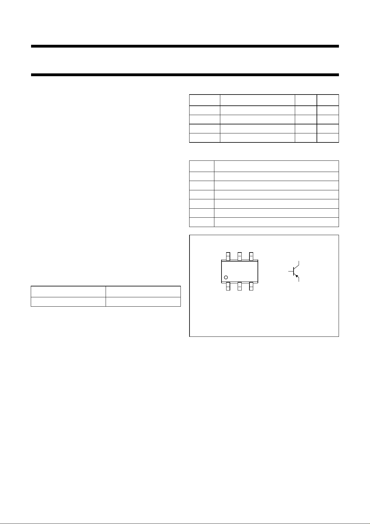
PINNING
PIN DESCRIPTION
1 collector
2 collector
3 base
4 emitter
5 collector
6 collector
collector-emitter voltage −40 V
peak collector current −3A
collector current (DC) −2A
equivalent on-resistance <200 mΩ
PNP low V
transistor in a SOT363 (SC-88) plastic
CEsat
package.
NPN complement: PBSS4240Y.
MARKING
TYPE NUMBER MARKING CODE
PBSS5240Y 52*
Note
1. * = p: made in Hongkong.
* = t: made in Malaysia.
(1)
handbook, halfpage
654
123
Top view
1, 2, 5, 6
3
4
MAM464
Fig.1 Simplified outline (SOT363; SC-88) and
symbol.
2002 Feb 28 2
Philips Semiconductors Product specification
40 V low V
PNP transistor
CEsat
PBSS5240Y
LIMITING VALUES
In accordance with the Absolute Maximum Rating System (IEC 60134).
SYMBOL PARAMETER CONDITIONS MIN. MAX. UNIT
V
CBO
V
CEO
V
EBO
I
C
I
CM
I
BM
P
tot
T
stg
T
j
T
amb
collector-base voltage open emitter −−40 V
collector-emitter voltage open base −−40 V
emitter-base voltage open collector −−5V
collector current (DC) −−2A
peak collector current −−3A
peak base current −−300 mA
total power dissipation T
≤ 25 °C; note 1 − 270 mW
amb
T
≤ 25 °C; note 2 − 430 mW
amb
storage temperature −65 +150 °C
junction temperature − 150 °C
operating ambient temperature −65 +150 °C
Notes
1. Device mounted on a printed-circuit board, single side copper, tinplated and standard footprint.
2. Device mounted on a printed-circuit board, single side copper, tinplated and mounting pad for collector 1 cm2.
THERMAL CHARACTERISTICS
SYMBOL PARAMETER CONDITIONS VALUE UNIT
R
th j-a
thermal resistance from junction to
ambient
note 1 463 K/W
note 2 291 K/W
Notes
1. Device mounted on a printed-circuit board, single side copper, tinplated and standard footprint.
2. Device mounted on a printed-circuit board, single side copper, tinplated and mounting pad for collector 1 cm2.
2002 Feb 28 3
 Loading...