

Philips PBSS5230T Technical data

查询PBSS5230T供应商
DISCRETE SEMICONDUCTORS
DATA SH EET
e
M3D088
PBSS5230T
30 V, 2 A
PNP low V
Product specification 2003 Dec 18
CEsat
(BISS) transistor
Philips Semiconductors Product specification
30 V, 2 A
PNP low V
CEsat
FEATURES
• Low collector-emitter saturation voltage V
• High collector current capability: IC and I
• Higher efficiency leading to less heat generation
• Reduced printed-circuit board requirements
• Cost effective alternative to MOSFETs in specific
applications.
APPLICATIONS
• Power management
– DC/DC converters
– Supply line switching
– Battery charger
– LCD backlighting.
• Peripheral drivers
– Driver in low supply voltage applications (e.g. lamps
and LEDs)
– Inductive load driver (e.g. relays,
buzzers and motors).
(BISS) transistor
CEsat
CM
PBSS5230T
QUICK REFERENCE DATA
SYMBOL PARAMETER MAX. UNIT
V
CEO
I
C
I
CM
R
CEsat
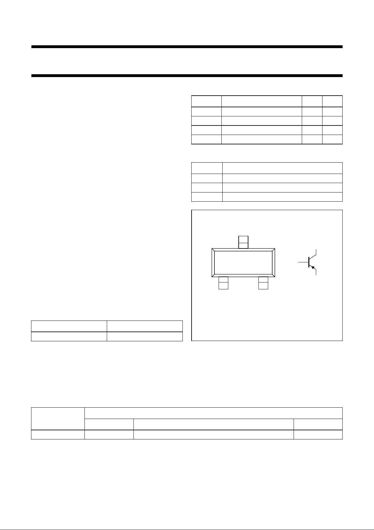
PINNING
PIN DESCRIPTION
handbook, halfpage
collector-emitter voltage −30 V
collector current (DC) −2A
peak collector current −3A
equivalent on-resistance 220 mΩ
1 base
2 emitter
3 collector
3
3
1
DESCRIPTION
PNP BISS transistor in a SOT23 plastic package offering
ultra low V
CEsat
and R
parameters.
CEsat
Top view
21
MAM256
2
MARKING
TYPE NUMBER MARKING CODE
(1)
Fig.1 Simplified outline (SOT23) and symbol.
PBSS5230T 3K*
Note
1. * = p: Made in Hong Kong.
* = t: Made in Malaysia.
* = W: Made in China.
ORDERING INFORMATION
PACKAGE
TYPE NUMBER
NAME DESCRIPTION VERSION
PBSS5230T − plastic surface mounted package; 3 leads SOT23
2003 Dec 18 2

Philips Semiconductors Product specification
30 V, 2 A
PBSS5230T
PNP low V
LIMITING VALUES
In accordance with the Absolute Maximum Rating System (IEC 60134).
SYMBOL PARAMETER CONDITIONS MIN. MAX. UNIT
V
CBO
V
CEO
V
EBO
I
C
I
CM
I
B
P
tot
T
j
T
amb
T
stg
Notes
1. Device mounted on a FR4 printed-circuit board; single-sided copper; tinplated; standard footprint.
2. Device mounted on a FR4 printed-circuit board; single-sided copper; tinplated; mounting pad for collector 1 cm2.
collector-base voltage open emitter −−30 V
collector-emitter voltage open base −−30 V
emitter-base voltage open collector −−5V
collector current (DC) −−2A
peak collector current single peak −−3A
base current (DC) −−300 mA
total power dissipation T
junction temperature − 150 °C
operating ambient temperature −65 +150 °C
storage temperature −65 +150 °C
(BISS) transistor
CEsat
≤ 25 °C; note 1 − 300 mW
amb
T
≤ 25 °C; note 2 − 480 mW
amb
THERMAL CHARACTERISTICS
SYMBOL PARAMETER CONDITIONS VALUE UNIT
R
th j-a
thermal resistance from junction to ambient in free air; note 1 417 K/W
in free air; note 2 260 K/W
Notes
1. Device mounted on a FR4 printed-circuit board; single-sided copper; tinplated; standard footprint.
2. Device mounted on a FR4 printed-circuit board; single-sided copper; tinplated; mounting pad for collector 1 cm2.
2003 Dec 18 3
 Loading...