


查询PBSS5160DS供应商
PBSS5160DS
60 V, 1 A PNP low V
Rev. 02 — 28 June 2005 Product data sheet
1. Product profile
1.1 General description
PNP/PNP low V
(SC-74) Surface Mounted Device (SMD) plastic package.
NPN complement: PBSS4160DS.
1.2 Features
■ Low collector-emitter saturation voltage V
■ High collector current capability: IC and I
■ High collector current gain (hFE) at high I
■ High efficiency due to less heat generation
■ Smaller required Printed-Circuit Board (PCB) area than for conventional transistors
(BISS) transistor
CEsat
Breakthrough in Small Signal (BISS) transistor pair in a SOT457
CEsat
CEsat
CM
C
1.3 Applications
■ Dual low power switches (e.g. motors, fans)
■ Automotive applications
1.4 Quick reference data
Table 1: Quick reference data
Symbol Parameter Conditions Min Typ Max Unit
V
CEO
I
C
I
CM
R
CEsat
[1] Device mounted on a ceramic PCB, Al2O3, standard footprint.
[2] Pulse test: tp≤ 300µs; δ≤0.02.
collector-emitter voltage open base - - −60 V
collector current (DC)
peak collector current single pulse;
t
≤ 1ms
p
collector-emitter saturation
resistance
IC= −1A;
I
= −100 mA
B
[1]
--−1A
--−2A
[2]
- 250 330 mΩ

Philips Semiconductors
PBSS5160DS
2. Pinning information
Table 2: Pinning
Pin Description Simplified outline Symbol
1 emitter TR1
2 base TR1
3 collector TR2
4 emitter TR2
5 base TR2
6 collector TR1
3. Ordering information
Table 3: Ordering information
Type number Package
PBSS5160DS SC-74 plastic surface mounted package; 6 leads SOT457
60 V, 1 A PNP low V
4
56
132
(BISS) transistor
CEsat
6
TR1
1
sym018
5
4
TR2
2
3
Name Description Version
4. Marking
Table 4: Marking codes
Type number Marking code
PBSS5160DS A5
5. Limiting values
Table 5: Limiting values
In accordance with the Absolute Maximum Rating System (IEC 60134).
Symbol Parameter Conditions Min Max Unit
Per transistor
V
CBO
V
CEO
V
EBO
I
C
I
CM
I
B
I
BM
collector-base voltage open emitter - −80 V
collector-emitter
open base - −60 V
voltage
emitter-base voltage open collector - −5V
collector current (DC)
[1]
- −0.77 A
[2]
- −0.9 A
[3]
- −1A
peak collector current single pulse; tp≤ 1ms - −2A
base current (DC) - −300 mA
peak base current single pulse; tp≤ 1ms - −1A
9397 750 15186 © Koninklijke Philips Electronics N.V. 2005. All rights reserved.
Product data sheet Rev. 02 — 28 June 2005 2 of 14
Philips Semiconductors
PBSS5160DS
Table 5: Limiting values
60 V, 1 A PNP low V
…continued
(BISS) transistor
CEsat
In accordance with the Absolute Maximum Rating System (IEC 60134).
Symbol Parameter Conditions Min Max Unit
P
tot
total power dissipation T
amb
≤ 25 °C
[1]
- 290 mW
[2]
- 370 mW
[3]
- 450 mW
Per device
P
tot
T
j
T
amb
T
stg
total power dissipation T
junction temperature - 150 °C
ambient temperature −65 +150 °C
storage temperature −65 +150 °C
amb
≤ 25 °C
[1] Device mounted on an FR4 PCB, single-sided copper, tin-plated and standard footprint.
[2] Device mounted on an FR4 PCB, single-sided copper, tin-plated, mounting pad for collector 1 cm2.
[3] Device mounted on a ceramic PCB, Al2O3, standard footprint.
[1]
- 420 mW
[2]
- 560 mW
[3]
- 700 mW
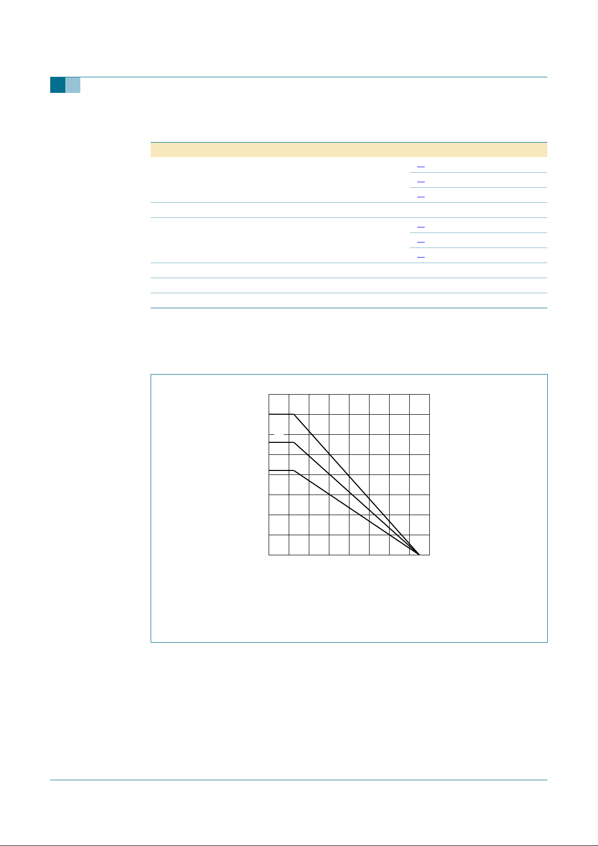
0.8
(1)
P
tot
(W)
0.6
(2)
(3)
0.4
0.2
0
0 16012040 80
(1) Ceramic PCB, Al2O3, standard footprint
(2) FR4 PCB, mounting pad for collector 1 cm
(3) FR4 PCB, standard footprint
Fig 1. Power derating curves
006aaa493
T
(°C)
amb
2
9397 750 15186 © Koninklijke Philips Electronics N.V. 2005. All rights reserved.
Product data sheet Rev. 02 — 28 June 2005 3 of 14
Philips Semiconductors
PBSS5160DS
6. Thermal characteristics
Table 6: Thermal characteristics
Symbol Parameter Conditions Min Typ Max Unit
Per transistor
R
th(j-a)
R
th(j-sp)
Per device
R
th(j-a)
[1] Device mounted on an FR4 PCB, single-sided copper, tin-plated and standard footprint.
[2] Device mounted on an FR4 PCB, single-sided copper, tin-plated, mounting pad for collector 1 cm2.
[3] Device mounted on a ceramic PCB, Al2O3, standard footprint.
thermal resistance from
junction to ambient
thermal resistance from
junction to solder point
thermal resistance from
junction to ambient
in free air
in free air
60 V, 1 A PNP low V
[1]
- - 431 K/W
[2]
- - 338 K/W
[3]
- - 278 K/W
- - 105 K/W
[1]
- - 298 K/W
[2]
- - 223 K/W
[3]
- - 179 K/W
(BISS) transistor
CEsat
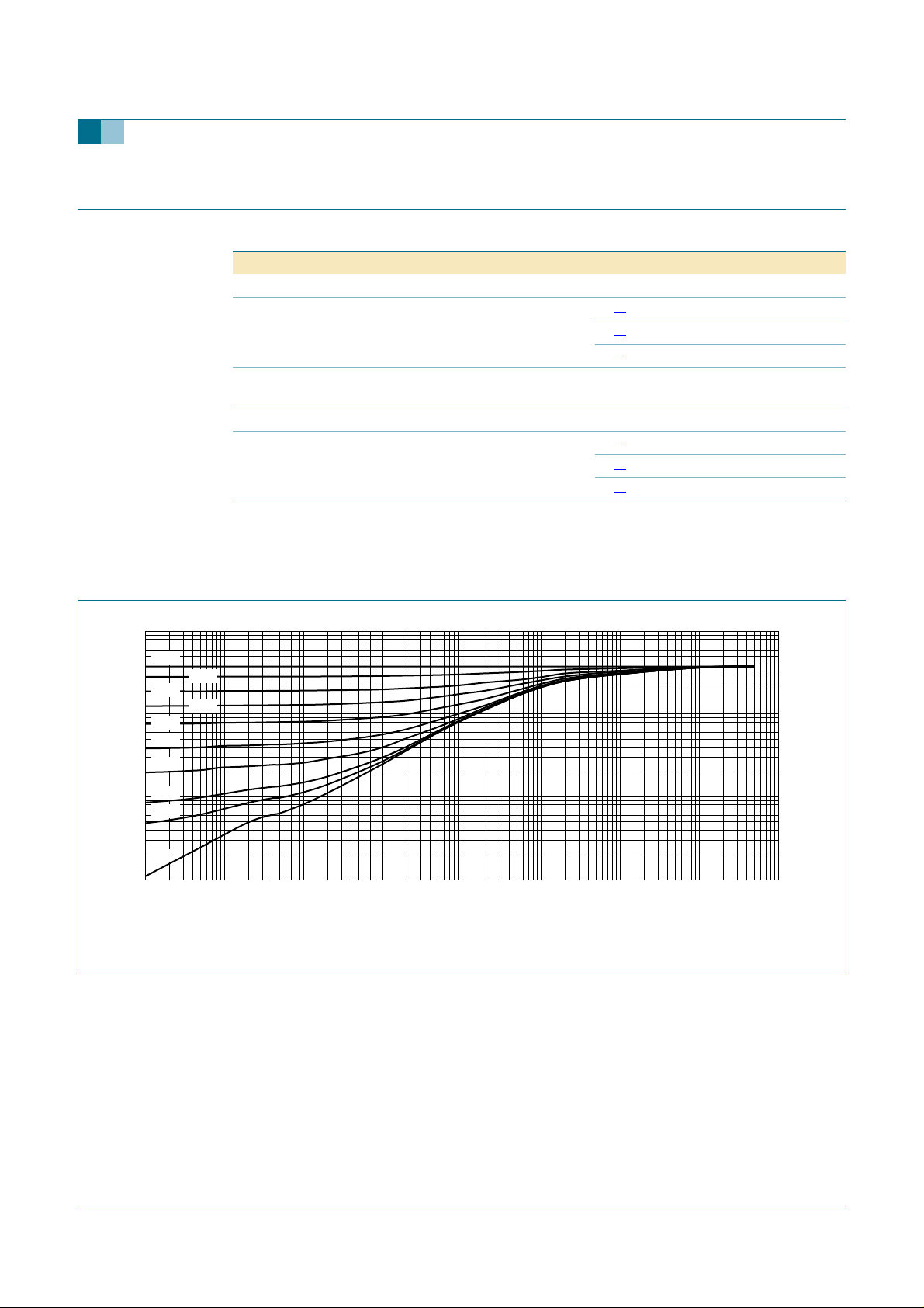
006aaa494
2
10
tp (s)
Z
th(j-a)
(K/W)
3
10
δ = 1
0.75
0.50
0.20
0.10
0.05
0.02
0.01
0
0.33
−4
10
−3
10
−2
−1
10
1
1010
2
10
10
1
−5
10
FR4 PCB, standard footprint
Fig 2. Transient thermal impedance from junction to ambient as a function of pulse time; typical values
3
10
9397 750 15186 © Koninklijke Philips Electronics N.V. 2005. All rights reserved.
Product data sheet Rev. 02 — 28 June 2005 4 of 14
Philips Semiconductors
PBSS5160DS
3
10
Z
th(j-a)
(K/W)
δ = 1
0.75
0.50
2
10
10
1
−5
10
0.20
0.10
0.05
0.02
0.01
0.33
0
−4
10
10
FR4 PCB, mounting pad for collector 1 cm
60 V, 1 A PNP low V
−3
−2
2
−1
10
1
1010
(BISS) transistor
CEsat
006aaa495
2
10
tp (s)
Fig 3. Transient thermal impedance from junction to ambient as a function of pulse time; typical values
3
10
006aaa496
3
10
Z
th(j-a)
(K/W)
δ = 1
0.75
0.50
2
10
10
1
10
−5
0.20
0.10
0.05
0.02
0.01
0
0.33
−4
10
−3
10
−2
−1
10
1
1010
2
10
tp (s)
Ceramic PCB, Al2O3, standard footprint
Fig 4. Transient thermal impedance from junction to ambient as a function of pulse time; typical values
3
10
9397 750 15186 © Koninklijke Philips Electronics N.V. 2005. All rights reserved.
Product data sheet Rev. 02 — 28 June 2005 5 of 14
 Loading...