

Philips PBSS5140V Technical data
查询PBSS5140V供应商
DISCRETE SEMICONDUCTORS
DATA SH EET
M3D744
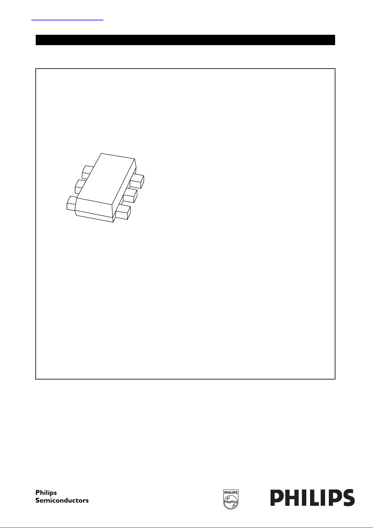
PBSS5140V
40 V low V
Product specification
Supersedes data of 2001 Oct 19
CEsat
PNP transistor
2002 Mar 20
Philips Semiconductors Product specification
40 V low V
CEsat
PNP transistor
FEATURES
• 300 mW total power dissipation
• Very small 1.6 mm × 1.2 mm × 0.55 mm ultra thin
package
• Improved thermal behaviour due to flat leads
• Self alignment during soldering due to straight leads
• Low collector-emitter saturation voltage
• High current capability
APPLICATIONS
• General purpose switching and muting
• LCD back lighting
• Supply line switching circuits
• Battery driven equipment (mobile phones, video
cameras and hand-held devices).
DESCRIPTION
PBSS5140V
QUICK REFERENCE DATA
SYMBOL PARAMETER MAX. UNIT
V
CEO
I
C
I
CM
R
CEsat
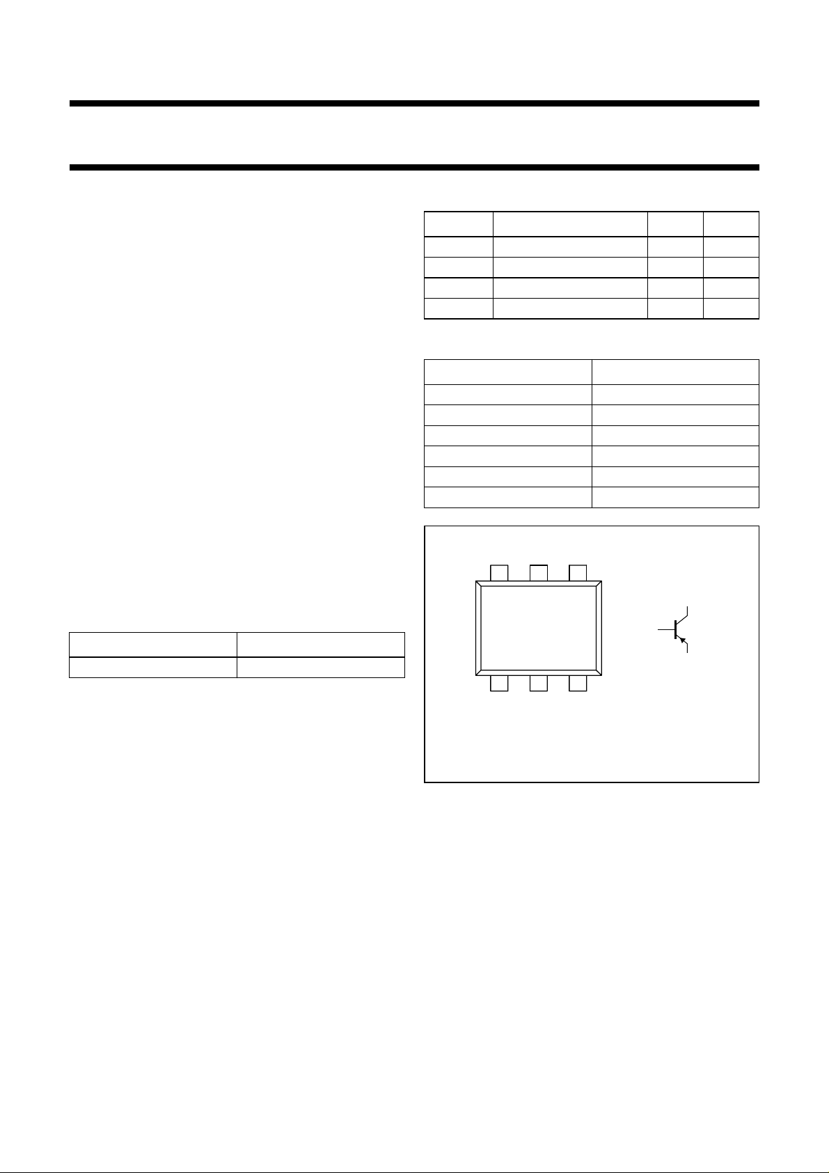
PINNING
collector-emitter voltage −40 V
collector current (DC) −1A
peak collector current −2A
equivalent on-resistance <340 mΩ
PIN DESCRIPTION
1 collector
2 collector
3 base
4 emitter
5 collector
6 collector
PNP low V
transistor in a SOT666 plastic package.
CE sat
NPN complement: PBSS4140V.
MARKING
TYPE NUMBER MARKING CODE
PBSS5140V 25
handbook, halfpage
Top view
5
46
123
MAM446
3
Fig.1 Simplified outline (SOT666) and symbol.
1, 2, 5, 6
4
2002 Mar 20 2
Philips Semiconductors Product specification
40 V low V
PNP transistor
CEsat
PBSS5140V
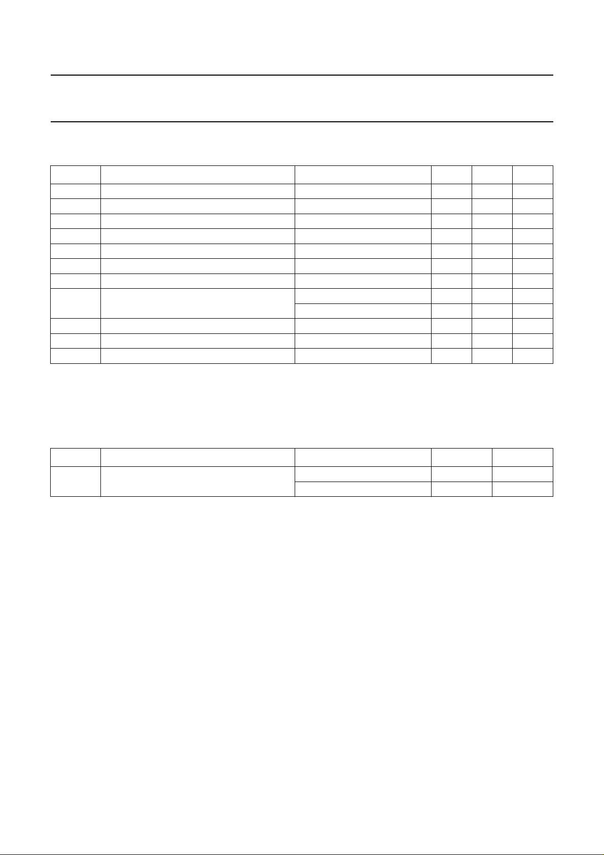
LIMITING VALUES
In accordance with the Absolute Maximum Rating System (IEC 60134).
SYMBOL PARAMETER CONDITIONS MIN. MAX. UNIT
V
CBO
V
CEO
V
EBO
I
C
I
CM
I
B
I
BM
P
tot
T
stg
T
j
T
amb
collector-base voltage open emitter −−40 V
collector-emitter voltage open base −−40 V
emitter-base voltage open collector −−5V
collector current (DC) −−1A
peak collector current −−2A
base current (DC) −−300 mA
peak base current −−1A
total power dissipation T
≤ 25 °C; note 1 − 300 mW
amb
≤ 25 °C; note 2 − 500 mW
T
amb
storage temperature −65 +150 °C
junction temperature − 150 °C
operating ambient temperature −65 +150 °C
Notes
1. Device mounted on a printed-circuit board, single side copper, tinplated and standard footprint.
2. Device mounted on a printed-circuit board, single side copper, tinplated and mounting pad for collector 1 cm
2
.
THERMAL CHARACTERISTICS
SYMBOL PARAMETER CONDITIONS VALUE UNIT
R
th j-a
thermal resistance from junction to ambient note 1 410 K/W
note 2 215 K/W
Notes
1. Device mounted on a printed-circuit board, single side copper, tinplated and standard footprint.
2. Device mounted on a printed-circuit board, single side copper, tinplated and mounting pad for collector 1 cm2.
Soldering
The only recommended soldering is reflow soldering.
2002 Mar 20 3
 Loading...