

Philips PBSS4320X User Manual
查询PBSS4320X供应商
DISCRETE SEMICONDUCTORS
DATA SH EET
ook, halfpage
M3D109
PBSS4320X
20 V, 3 A
NPN low V
Product specification
Supersedes data of 2003 Dec 15
CEsat
(BISS) transistor
2004 Nov 03
Philips Semiconductors Product specification
20 V, 3 A
NPN low V
CEsat
FEATURES
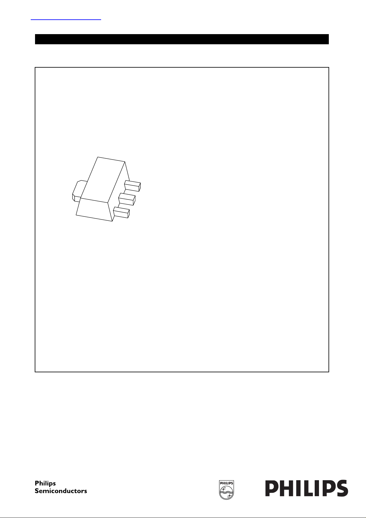
• SOT89 (SC-62) package
• Low collector-emitter saturation voltage V
• High collector current capability: IC and I
• Higher efficiency leading to less heat generation
• Reduced printed-circuit board requirements.
APPLICATIONS
• Power management
– DC/DC converters
– Supply line switching
– Battery charger
– LCD backlighting.
• Peripheral drivers
– Driver in low supply voltage applications (e.g. lamps
and LEDs).
– Inductive load driver (e.g. relays,
buzzers and motors).
(BISS) transistor
CEsat
CM
PBSS4320X
QUICK REFERENCE DATA
SYMBOL PARAMETER MAX. UNIT
V
CEO
I
C
I
CM
R
CEsat
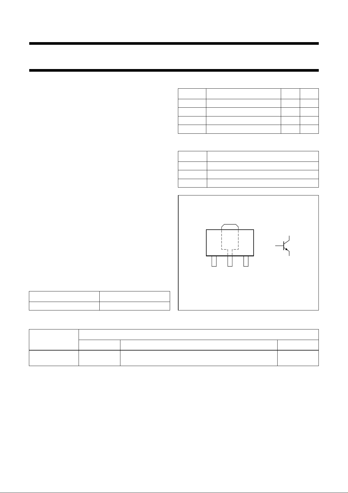
PINNING
PIN DESCRIPTION
collector-emitter voltage 20 V
collector current (DC) 3 A
peak collector current 5 A
equivalent on-resistance 105 mΩ
1 emitter
2 collector
3 base
2
DESCRIPTION
NPN low V
PNP complement: PBSS5320X.
transistor in a SOT89 plastic package.
CEsat
321
MARKING
TYPE NUMBER MARKING CODE
Fig.1 Simplified outline (SOT89) and symbol.
PBSS4320X S44
ORDERING INFORMATION
PACKAGE
TYPE NUMBER
NAME DESCRIPTION VERSION
PBSS4320X SC-62 plastic surface mounted package; collector pad for good heat
transfer; 3 leads
3
1
sym042
SOT89
2004 Nov 03 2
Philips Semiconductors Product specification
20 V, 3 A
PBSS4320X
NPN low V
LIMITING VALUES
In accordance with the Absolute Maximum Rating System (IEC 60134).
SYMBOL PARAMETER CONDITIONS MIN. MAX. UNIT
V
V
V
I
I
I
P
T
T
T
CBO
CEO
EBO
C
CM
B
tot
stg
j
amb
collector-base voltage open emitter − 20 V
collector-emitter voltage open base − 20 V
emitter-base voltage open collector − 5V
collector current (DC) note 4 − 3A
peak collector current limited by T
base current (DC) − 0.5 A
total power dissipation T
storage temperature −65 +150 °C
junction temperature − 150 °C
ambient temperature −65 +150 °C
(BISS) transistor
CEsat
− 5A
amb
j(max)
≤ 25 °C
note 1 − 550 mW
note 2 − 1W
note 3 − 1.4 W
note 4 − 1.6 W
Notes
1. Device mounted on a FR4 printed-circuit board; single-sided copper; tin-plated; standard footprint.
2. Device mounted on a FR4 printed-circuit board; single-sided copper; tin-plated; mounting pad for collector 1 cm2.
3. Device mounted on a FR4 printed-circuit board; single-sided copper; tin-plated; mounting pad for collector 6 cm2.
4. Device mounted on a ceramic printed-circuit board 7 cm2, single-sided copper, tin-plated.
2004 Nov 03 3
Philips Semiconductors Product specification
20 V, 3 A
NPN low V
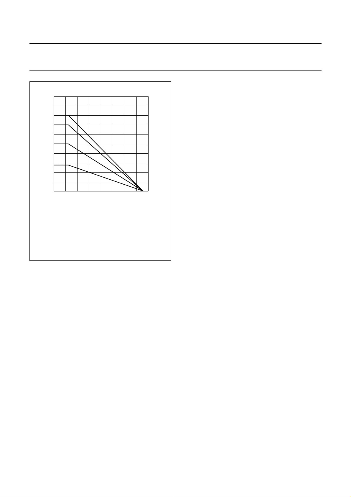
handbook, halfpage
2
P
tot
(W)
(1)
1.6
(2)
1.2
(3)
0.8
(4)
0.4
0
0 40 80 160
(1) Ceramic PCB; 7 cm
mounting pad for collector.
(2) FR4 PCB; 6 cm2 copper
mounting pad for collector.
(BISS) transistor
CEsat
2
(3) FR4 PCB; 1 cm
mounting pad for collector.
(4) Standard footprint.
120
T
amb
MLE372
(°C)
2
copper
PBSS4320X
Fig.2 Power derating curves.
2004 Nov 03 4
 Loading...