

Philips PBSS3540M User Guide
查询PBSS3540M供应商
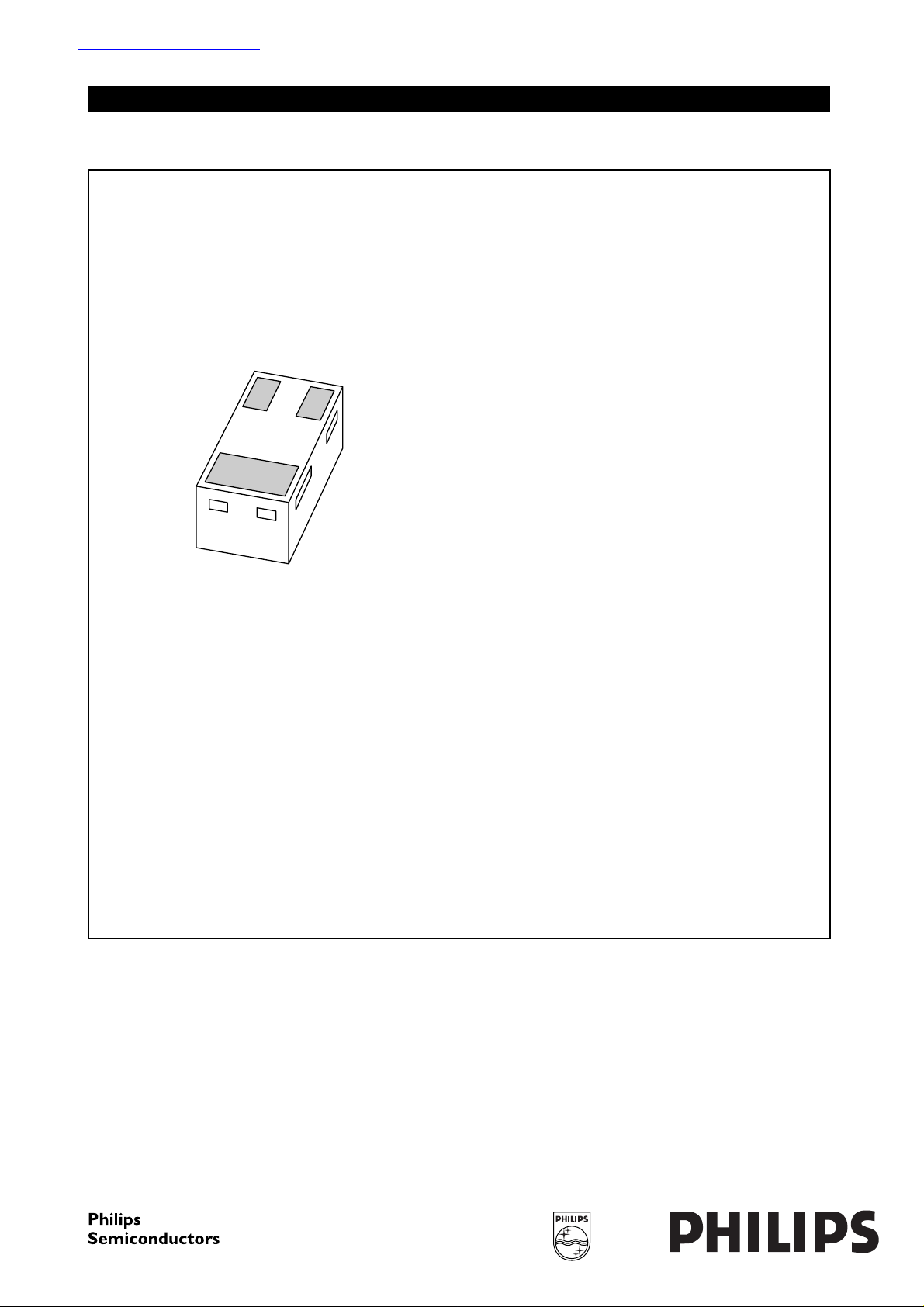
DISCRETE SEMICONDUCTORS
DATA SH EET
M3D883
BOTTOM VIEW
PBSS3540M
40 V, 0.5 A
PNP low V
Product specification 2003 Aug 12
CEsat
(BISS) transistor

Philips Semiconductors Product specification
40 V, 0.5 A
PNP low V
CEsat
FEATURES
• Low collector-emitter saturation voltage V
• High collector current capability IC and I
• High efficiency leading to reduced heat generation
• Reduced printed-circuit board requirements.
APPLICATIONS
• Power management:
– DC-DC converter
– Supply line switching
– Battery charger
– LCD backlighting.
• Peripheral driver:
– Driver in low supply voltage applications (e.g. lamps
and LEDs).
– Inductive load drivers (e.g. relays, buzzers and
motors).
DESCRIPTION
Low V
PNP transistor in a SOT883 leadless ultra
CEsat
small plastic package.
NPN complement: PBSS2540M.
(BISS) transistor
CEsat
CM
PBSS3540M
QUICK REFERENCE DATA
SYMBOL PARAMETER MAX. UNIT
V
CEO
I
C
I
CM
R
CEsat
PINNING
PIN DESCRIPTION
1 base
2 emitter
3 collector
handbook, halfpage
collector-emitter voltage −40 V
collector current (DC) −500 mA
peak collector current −1A
equivalent on-resistance <700 mΩ
2
1
Bottom view
3
MAM469
3
1
2
MARKING
TYPE NUMBER MARKING CODE
PBSS3540M DA
Fig.1 Simplified outline (SOT883) and symbol.
2003 Aug 12 2
Philips Semiconductors Product specification
40 V, 0.5 A
PBSS3540M
PNP low V
LIMITING VALUES
In accordance with the Absolute Maximum Rating System (IEC 60134).
SYMBOL PARAMETER CONDITIONS MIN. MAX. UNIT
V
CBO
V
CEO
V
EBO
I
C
I
CM
I
BM
P
tot
T
stg
T
j
T
amb
Notes
1. Refer to SOT883 standard mounting conditions.
2. Device mounted on an FR4 printed-circuit board, single-sided copper, tinplated, standard footprint, with 60 µm
copper strip line.
3. Device mounted on a printed-circuit board, single-sided copper, tinplated, mounting pad for collector 1 cm2.
collector-base voltage open emitter −−40 V
collector-emitter voltage open base −−40 V
emitter-base voltage open collector −−6V
collector current (DC) notes 1 and 2 −−500 mA
peak collector current −−1A
peak base current −−100 mA
total power dissipation T
storage temperature −65 +150 °C
junction temperature − 150 °C
operating ambient temperature −65 +150 °C
(BISS) transistor
CEsat
≤ 25 °C; notes 1 and 2 − 250 mW
amb
T
≤ 25 °C; note 1 and 3 − 430 mW
amb
THERMAL CHARACTERISTICS
SYMBOL PARAMETER CONDITIONS VALUE UNIT
R
th j-a
thermal resistance from junction to
ambient
in free air; notes 1 and 2 500 K/W
in free air; notes 1, 3 and 4 290 K/W
Notes
1. Refer to SOT883 standard mounting conditions.
2. Device mounted on an FR4 printed-circuit board, single-sided copper, tinplated, standard footprint, with 60 µm
copper strip line.
3. Device mounted on a printed-circuit board, single-sided copper, tinplated, mounting pad for collector 1 cm2.
4. Operated under pulsed conditions: duty cycle δ≤20%, pulse width tp≤ 30 ms.
Soldering
Reflow soldering is the only recommended soldering method.
2003 Aug 12 3
 Loading...