

Philips PBSS3540F Technical data

查询PBSS3540F供应商
DISCRETE SEMICONDUCTORS
DATA SH EET
M3D425
PBSS3540F
40 V low V
Product specification 2001 Jul 13
CEsat
PNP transistor
Philips Semiconductors Product specification
40 V low V
CEsat
PNP transistor
FEATURES
• Low collector-emitter saturation voltage
• High current capability
• Improved thermal behaviour due to flat leads
• Enhanced performance over SOT23 general purpose
transistors.
APPLICATIONS
• General purpose switching and muting
• Low frequency driver circuits
• Audio frequency general purpose applications
• Battery driven equipment (mobile phones, video
cameras, hand-held devices).
DESCRIPTION
PNP low V
transistor in a SC-89 (SOT490) plastic
CEsat
package.
NPN complement: PBSS2540F.
PBSS3540F
QUICK REFERENCE DATA
SYMBOL PARAMETER MAX. UNIT
V
CEO
I
CM
R
CEsat
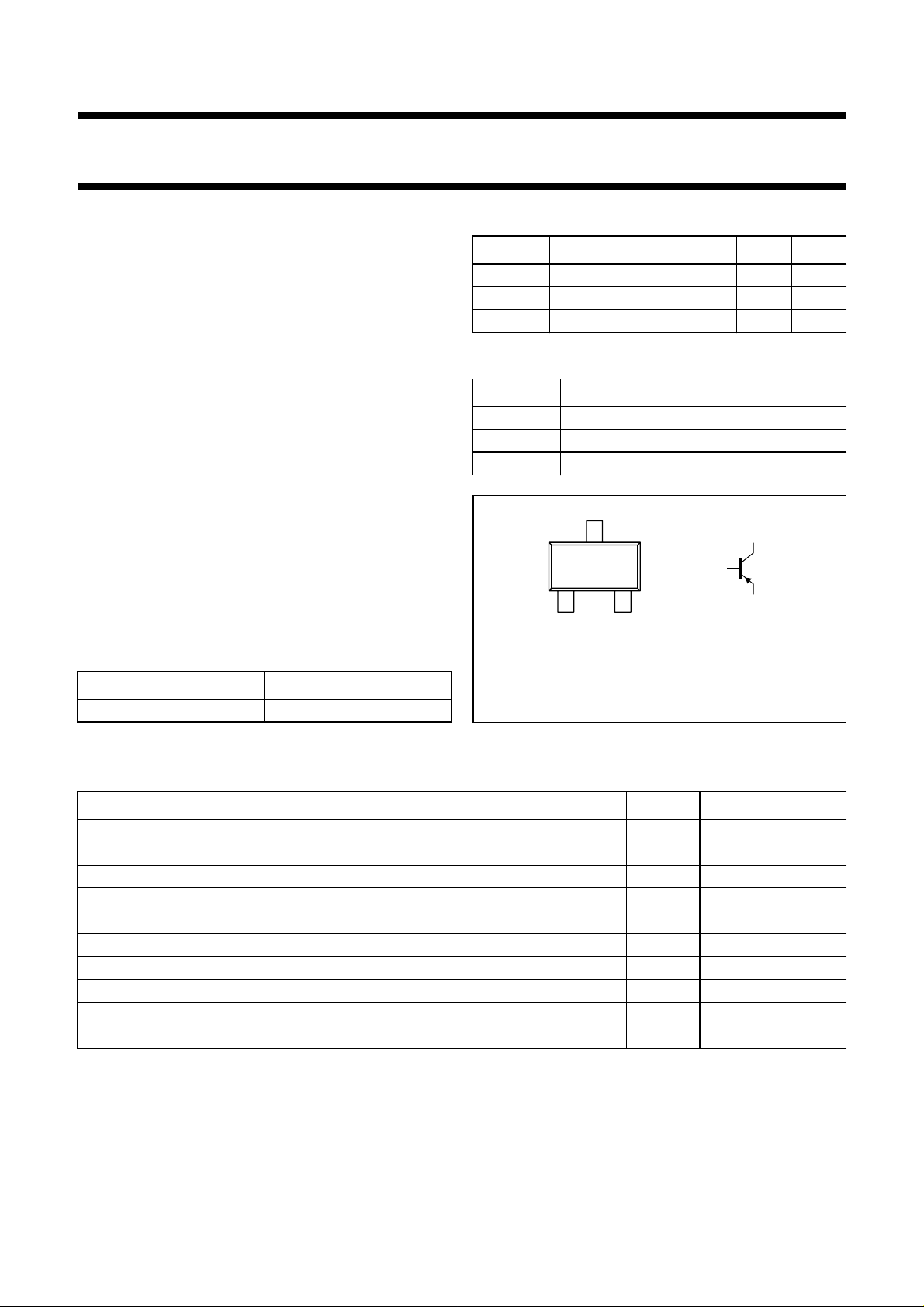
PINNING
PIN DESCRIPTION
handbook, halfpage
collector-emitter voltage −40 V
peak collector current −1A
equivalent on-resistance <700 mΩ
1 base
2 emitter
3 collector
3
1
12
Top view
MAM411
3
2
MARKING
TYPE NUMBER MARKING CODE
Fig.1 Simplified outline (SC-89; SOT490) and
symbol.
PBSS3540F 2D
LIMITING VALUES
In accordance with the Absolute Maximum Rating System (IEC 60134).
SYMBOL PARAMETER CONDITIONS MIN. MAX. UNIT
V
CBO
V
CEO
V
EBO
I
C
I
CM
I
BM
P
tot
T
stg
T
j
T
amb
collector-base voltage open emitter −−40 V
collector-emitter voltage open base −−40 V
emitter-base voltage open collector −−6V
collector current (DC) −−500 mA
peak collector current −−1A
peak base current −−100 mA
total power dissipation T
≤ 25 °C − 250 mW
amb
storage temperature −65 +150 °C
junction temperature − 150 °C
operating ambient temperature −65 +150 °C
2001 Jul 13 2

Philips Semiconductors Product specification
40 V low V
PNP transistor
CEsat
PBSS3540F
THERMAL CHARACTERISTICS
SYMBOL PARAMETER CONDITIONS VALUE UNIT
R
th j-a
thermal resistance from junction to ambient in free air 500 K/W
CHARACTERISTICS
T
=25°C unless otherwise specified.
amb
SYMBOL PARAMETER CONDITIONS MIN. TYP. MAX. UNIT
I
CBO
I
BEO
h
FE
V
CEsat
R
CEsat
V
BEsat
V
BEon
C
c
f
T
collector-base cut-off current VCB= −40 V; IE=0 −−−100 nA
V
= −40 V; IE= 0; Tj= 150 °C −−−50 µA
CB
emitter-base cut-off current VEB= −5 V; IC=0 −−−100 nA
DC current gain VCE= −2V
I
=−10 mA 200 −−
C
I
=−100 mA; note 1 150 −−
C
I
=−500 mA; note 1 40 −−
C
collector-emitter saturation voltage IC= −10 mA; IB= −0.5 mA −−−50 mV
I
= −100 mA; IB= −5mA −−−130 mV
C
I
= −200 mA; IB= −10 mA −−−200 mV
C
I
= −500 A; IB= −50 mA; note 1 −−−350 mV
C
equivalent on-resistance IC= −500 mA; IB= −50 mA; note 1 − 440 <700 mΩ
base-emitter saturation voltage IC= −500 mA; IB= −50 mA; note 1 −−−1.2 V
base-emitter turn-on voltage VCE= −2 V; IC= −100 mA; note 1 −−−1.1 V
collector capacitance VCB= −10 V; IE=Ie= 0; f = 1 MHz −−10 pF
transition frequency IC= −100 mA; VCE= −5V;
100 300 − MHz
f = 100 MHz
Note
1. Pulse test: t
≤ 300 ms; δ≤0.02.
p
2001 Jul 13 3
 Loading...