

Philips PBSS3515VS Datasheet
DISCRETE SEMICONDUCTORS
DATA SH EET
M3D744
PBSS3515VS
15 V low V
CEsat
transistor
Product specification
Supersedes data of 2001 Sep 27
PNP double
2001 Nov 07
Philips Semiconductors Product specification
15 V low V
CEsat
PNP double transistor
FEATURES
• 300 mW total power dissipation
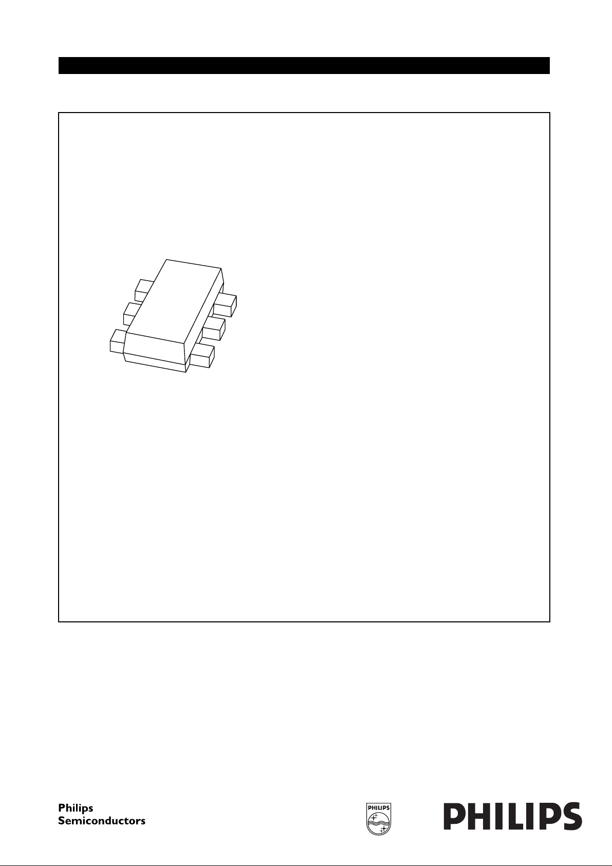
• Very small 1.6 x 1.2 mm ultra thin package
• Self alignment during soldering due to straight leads
• Low collector-emitter saturation voltage
• High current capability
• Improved thermal behaviour due to flat leads
• Replaces two SC75/SC89 packaged low V
CEsat
transistors on same PCB area
• Reduces required PCB area
• Reduced pick and place costs.
APPLICATIONS
• General purpose switching and muting
• Low frequency driver circuits
• LCD backlighting
• Audio frequency general purpose amplifier applications
• Battery driven equipment (mobile phones, video
cameras and hand-held devices).
PBSS3515VS
QUICK REFERENCE DATA
SYMBOL PARAMETER MAX. UNIT
V
CEO
I
CM
R
CEsat
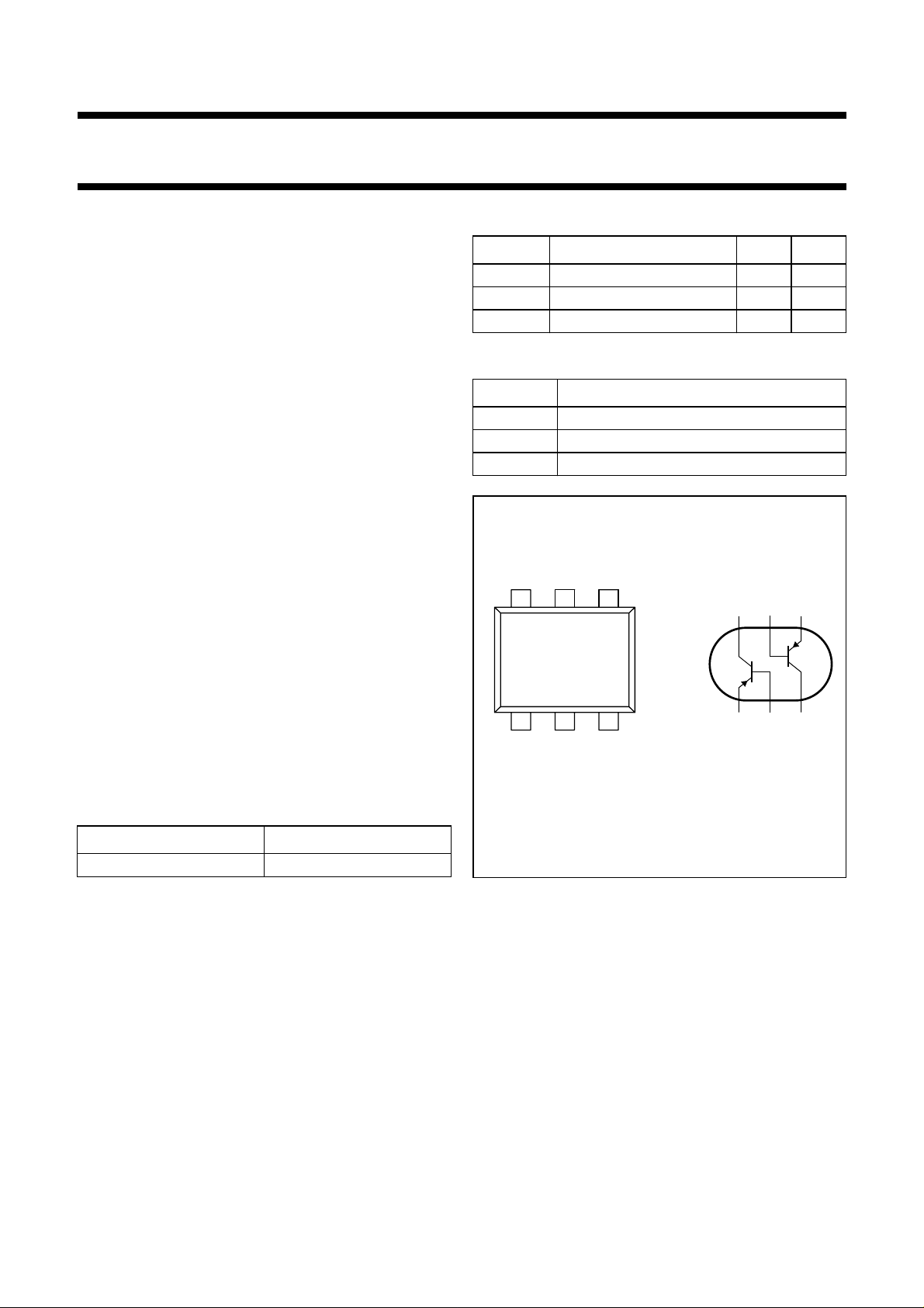
PINNING
PIN DESCRIPTION
1, 4 emitter TR1; TR2
2, 5 base TR1; TR2
6, 3 collector TR1; TR2
collector-emitter voltage −15 V
peak collector current −1A
equivalent on-resistance <500 mΩ
465
645
TR2
TR1
DESCRIPTION
PNP low V
double transistor in a SOT666 plastic
CEsat
package.
NPN complement: PBSS2515VS.
MARKING
TYPE NUMBER MARKING CODE
PBSS3515VS 35
123
Top view
MAM450
132
Fig.1 Simplified outline (SOT666) and symbol.
2001 Nov 07 2
Philips Semiconductors Product specification
15 V low V
PNP double transistor
CEsat
PBSS3515VS
LIMITING VALUES
In accordance with the Absolute Maximum Rating System (IEC 60134).
SYMBOL PARAMETER CONDITIONS MIN. MAX. UNIT
Per transistor unless otherwise specified
V
CBO
V
CEO
V
EBO
I
C
I
CM
I
BM
P
tot
T
stg
T
j
T
amb
collector-base voltage open emitter −−15 V
collector-emitter voltage open base −−15 V
emitter-base voltage open collector −−6V
collector current (DC) −−500 mA
peak collector current −−1A
peak base current −−100 mA
total power dissipation T
≤ 25 °C; note 1 − 200 mW
amb
storage temperature −65 +150 °C
junction temperature − 150 °C
operating ambient temperature 65 +150 °C
Per device
P
tot
total power dissipation T
≤ 25 °C; note 1 − 300 mW
amb
Note
1. Transistor mounted on an FR4 printed-circuit board.
THERMAL CHARACTERISTICS
SYMBOL PARAMETER CONDITIONS VALUE UNIT
R
th j-a
thermal resistance from junction to ambient notes 1 and 2 416 K/W
Notes
1. Transistor mounted on an FR4 printed-circuit board.
2. The only recommended soldering method is reflow soldering.
2001 Nov 07 3

Philips Semiconductors Product specification
15 V low V
PNP double transistor
CEsat
PBSS3515VS
CHARACTERISTICS
T
=25°C unless otherwise specified.
amb
SYMBOL PARAMETER CONDITIONS MIN. TYP. MAX. UNIT
Per transistor unless otherwise specified
I
CBO
I
EBO
h
FE
V
CEsat
R
CEsat
V
BEsat
V
BE
f
T
collector-base cut-off current VCB= −15 V; IE=0 −−−100 nA
V
= −15 V; IE= 0; Tj= 150 °C −−−50 µA
CB
emitter-base cut-off current VEB= −5 V; IC=0 −−−100 nA
DC current gain VCE= −2 V; IC= −10 mA 200 −−
V
= −2 V; IC= −100 mA; note 1 150 −−
CE
V
= −2 V; IC= −500 mA; note 1 90 −−
CE
collector-emitter saturation
voltage
IC= −10 mA; IB= −0.5 mA −−−25 mV
I
= −200 mA; IB= −10 mA −−−150 mV
C
I
= −500 mA; IB= −50 mA; note 1 −−−250 mV
C
equivalent on-resistance IC= −500 mA; IB= −50 mA; note 1 − 300 <500 mΩ
base-emitter saturation voltage IC= −500 mA; IB= −50 mA; note 1 −−−1.1 V
base-emitter turn-on voltage VCE= −2 V; IC= −100 mA; note 1 −−−0.9 V
transition frequency IC= −100 mA; VCE= −5V;
100 280 − MHz
f = 100 MHz
C
c
collector capacitance VCB= −10 V; IE=Ie= 0; f = 1MHz −−10 pF
Note
1. Pulse test: t
≤ 300 µs; δ≤0.02.
p
2001 Nov 07 4
 Loading...