

Page 1

PHILIPS
PHILIPS SERVICE AND QUALITY/TRAINING
P8
POWER SUPPLY AND SIGNAL FLOW
PHILIPS
TECH
FORCE TRAIN
MANUALS
PHILIPS TECHNICAL TRAINING/QUALITY
ONE PHILIPS DRIVE
PO BOX 14810
KNOXVILLE, TN 37914-1810
PHONE: 865-521-4397
FAX: 865-521-4818
TRAINING
EMAIL: [email protected]
Page 2
Introduction
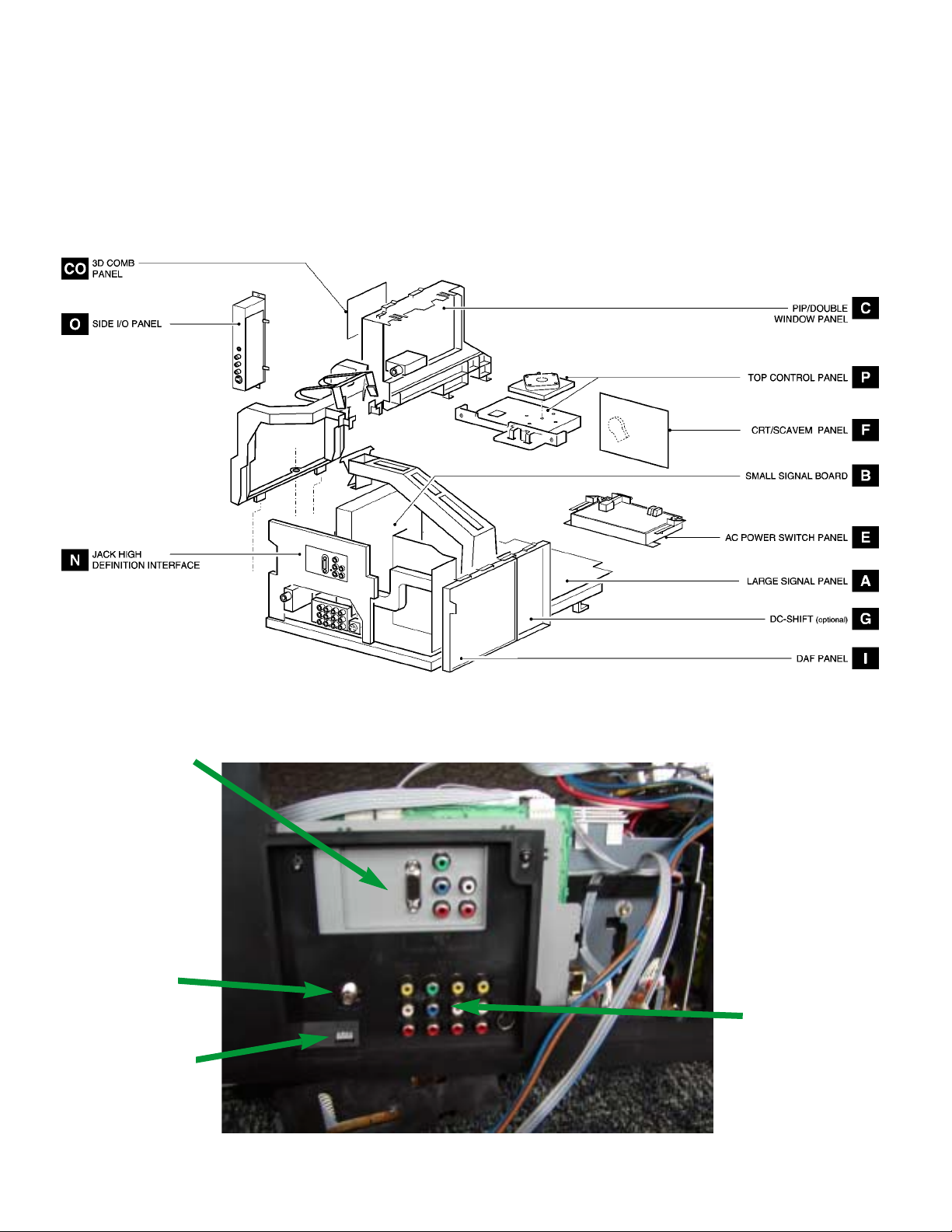
The P8 chassis is designed for the 2003 model year and is a step-down version of the R8. The primary difference is the microprocessor. The P8 uses a "Painter" instead of an "OTC".
Chassis architecture consists of a main board, referred to as the Large Signal Panel (LSP), a smaller, completely shielded, Small Signal Board (SSB) that is mounted on the LSP via an 80-pin Sim
connector, a PIP/DW panel, and a 3D Comb Filter board.
AV4
Main Tuner
ComPair Jack
P8 Architecture
AV1 - AV2
AV1, 2, 4 and Tuner
Page 3
The set is designed to accept RF, Component, and Composite signals utilizing NTSC, Progressive,
or 1080I (YPbPr) formats. It is available in two sizes: 30" and 34".
A line doubler is used to convert NTSC inputs to a progressive scan format.
There are four I/O (Jack Panels), referred to as AV1, AV2, AV3, and AV4. These jack panels offer
numerous inputs and outputs. AV4 is used specifically for High Definition Progressive Scan or 1080I
component input. These inputs can be either RGB or YPbPr type.
There are two versions of this chassis. The single tuner and two-tuner versions. When two tuners
are used, the second tuner is located on the PIP/DW board and is only used for reception of the PIP
signals.
The Audio circuitry consists of an MSP type audio demodulator/processor, a 15-watt (x2) Class "D"
audio amplifier, and a headphone amplifier.
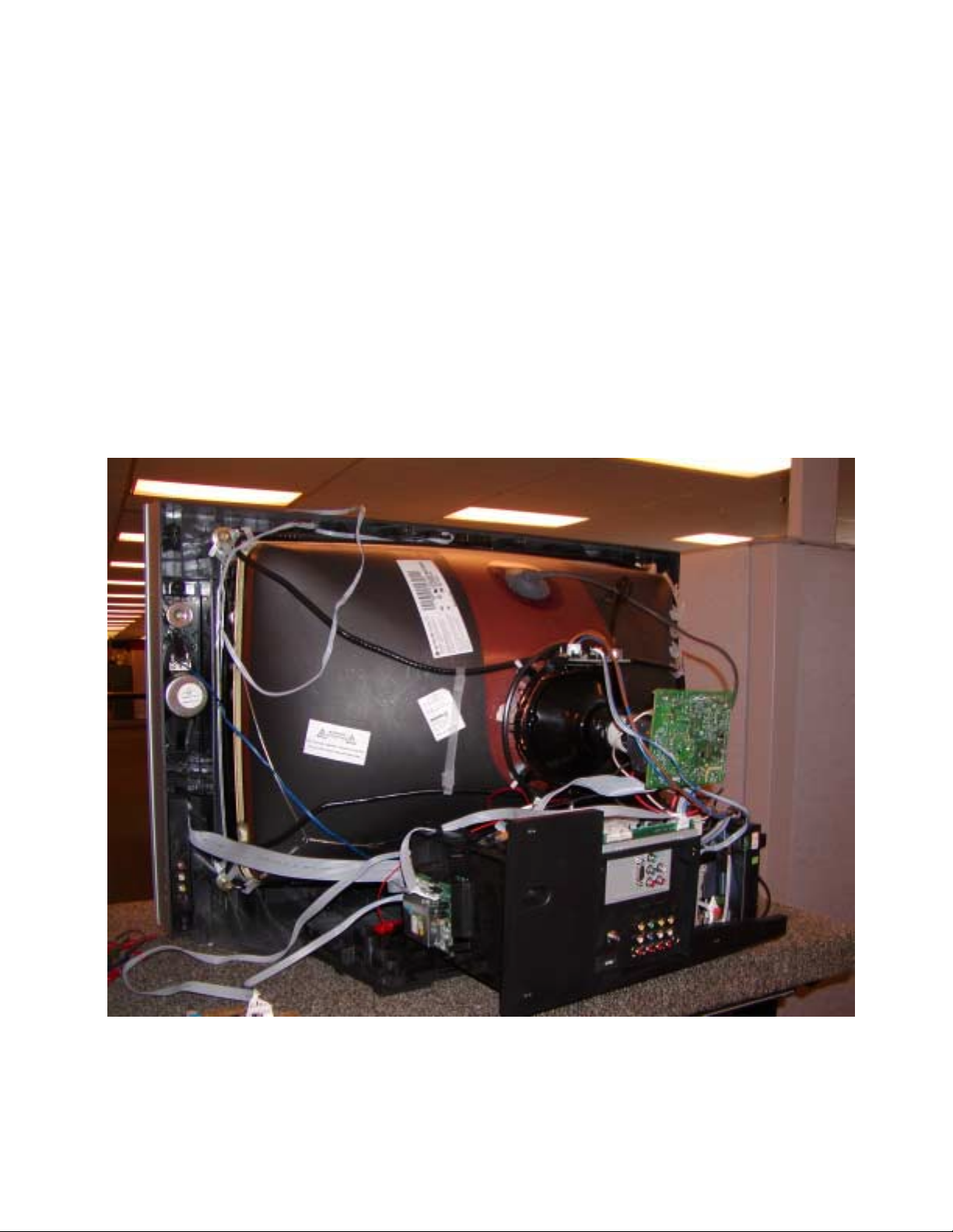
P8 Chassis Rear View
Page 4
Video Paths
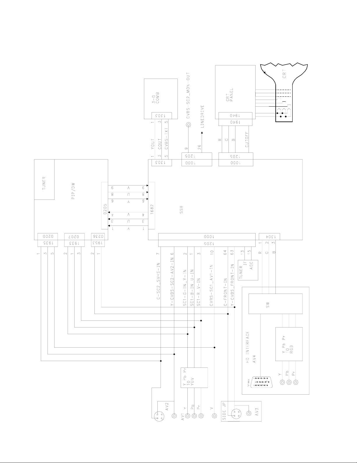
The P8 chassis has several video input/output connections (also with audio connections).
Figure 1 - Block
Page 5
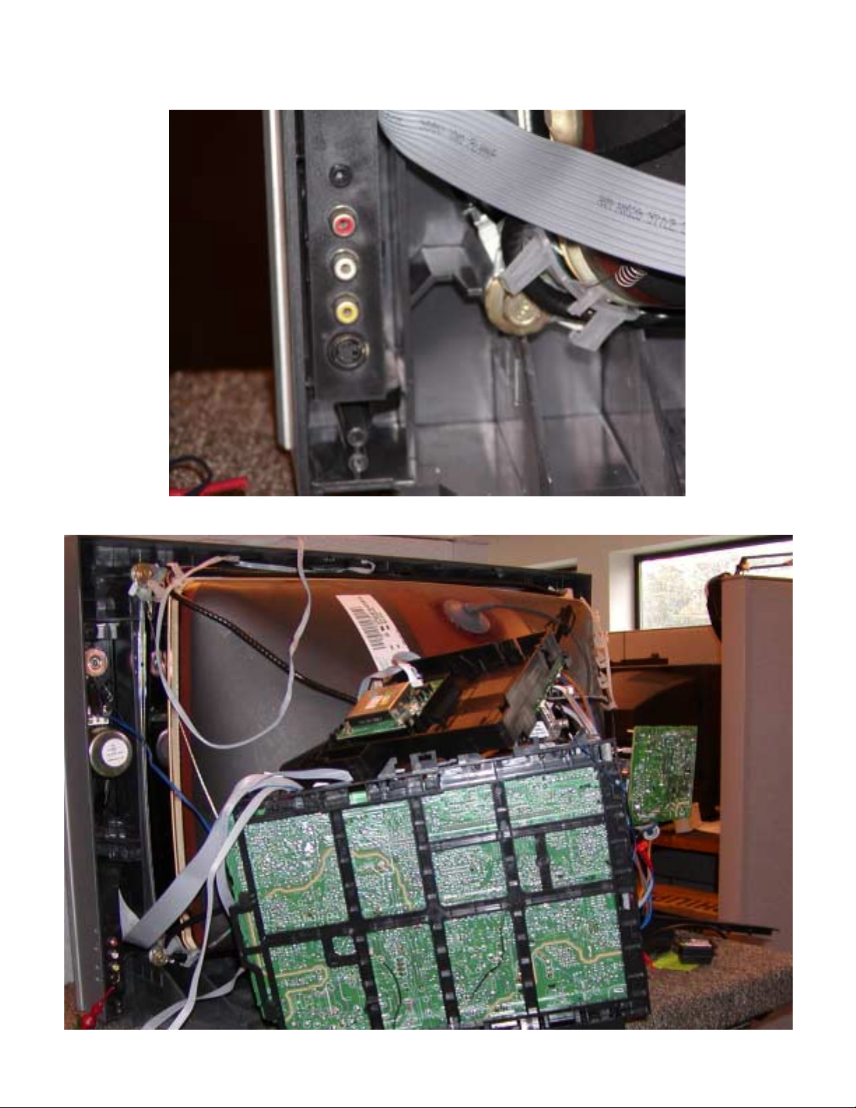
AV3, the Side Jack panel, provides connections for CVBS and Y/C (SVHS) inputs. This panel is
located on the left rear side of the cabinet (looking at it from the rear).
AV3 Closeup from Rear
P8 Service Position
Page 6
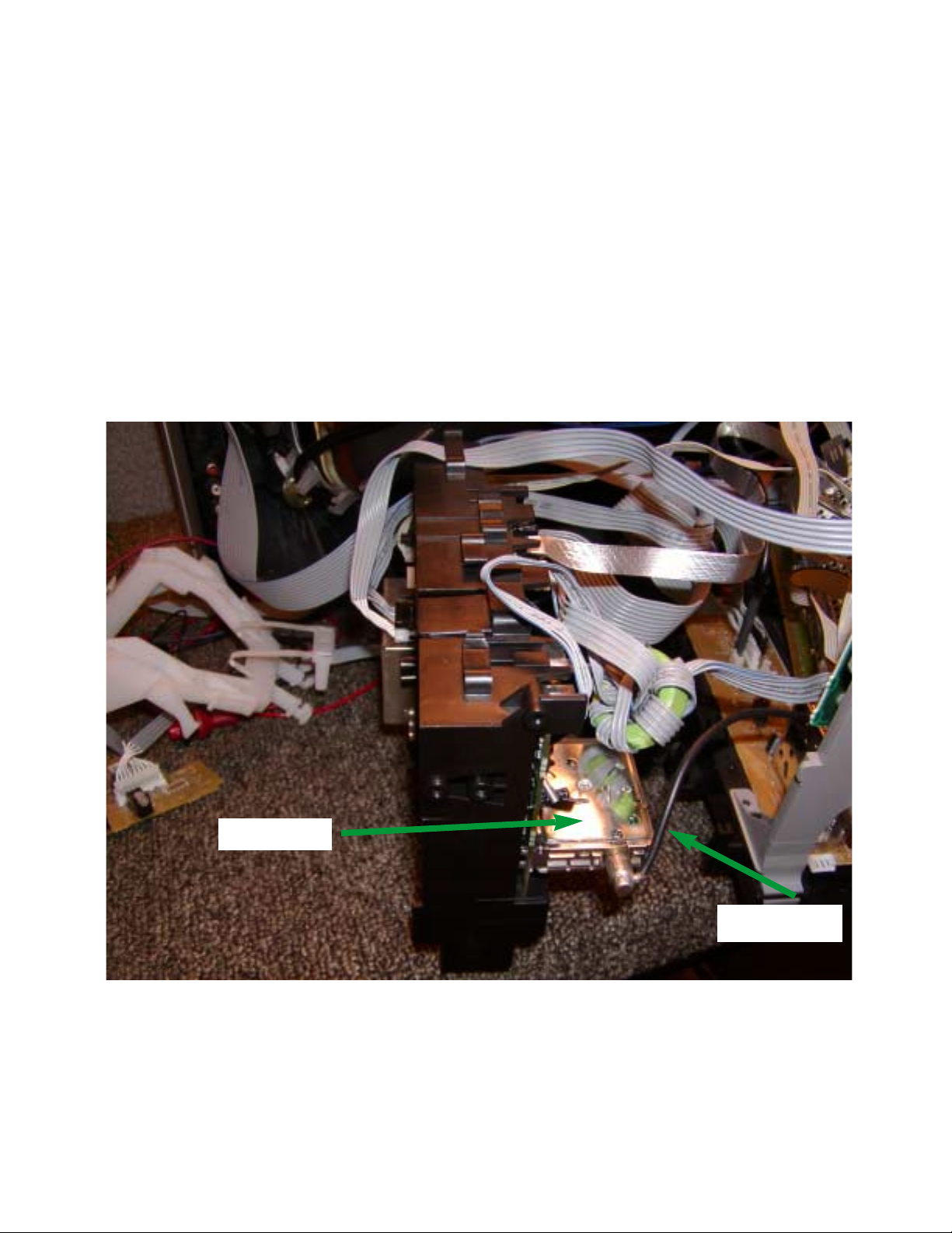
AV1 is mounted on the rear of the Large Signal panel (LSP) and provides connections for CVBS,
RGB, and YUV inputs.
AV2 is also mounted on the rear of the LSP and provides CVBS and YC (SVHS) inputs and a
CVBS, Monitor output.
AV4 is located on the High Definition Jack panel interface board and provides for YPbPr/RGB (HD
2fH) inputs.
This chassis is capable of DW (Dual Window) PIP. Because of this, the chassis employs two separate U/V tuners. One is mounted on the Large Signal (LSP) panel and the second one is located on
the PIP/DW panel.
PIP Tuner
Splitter Cable
PIP DW Panel and Comb Filter Board
Page 7
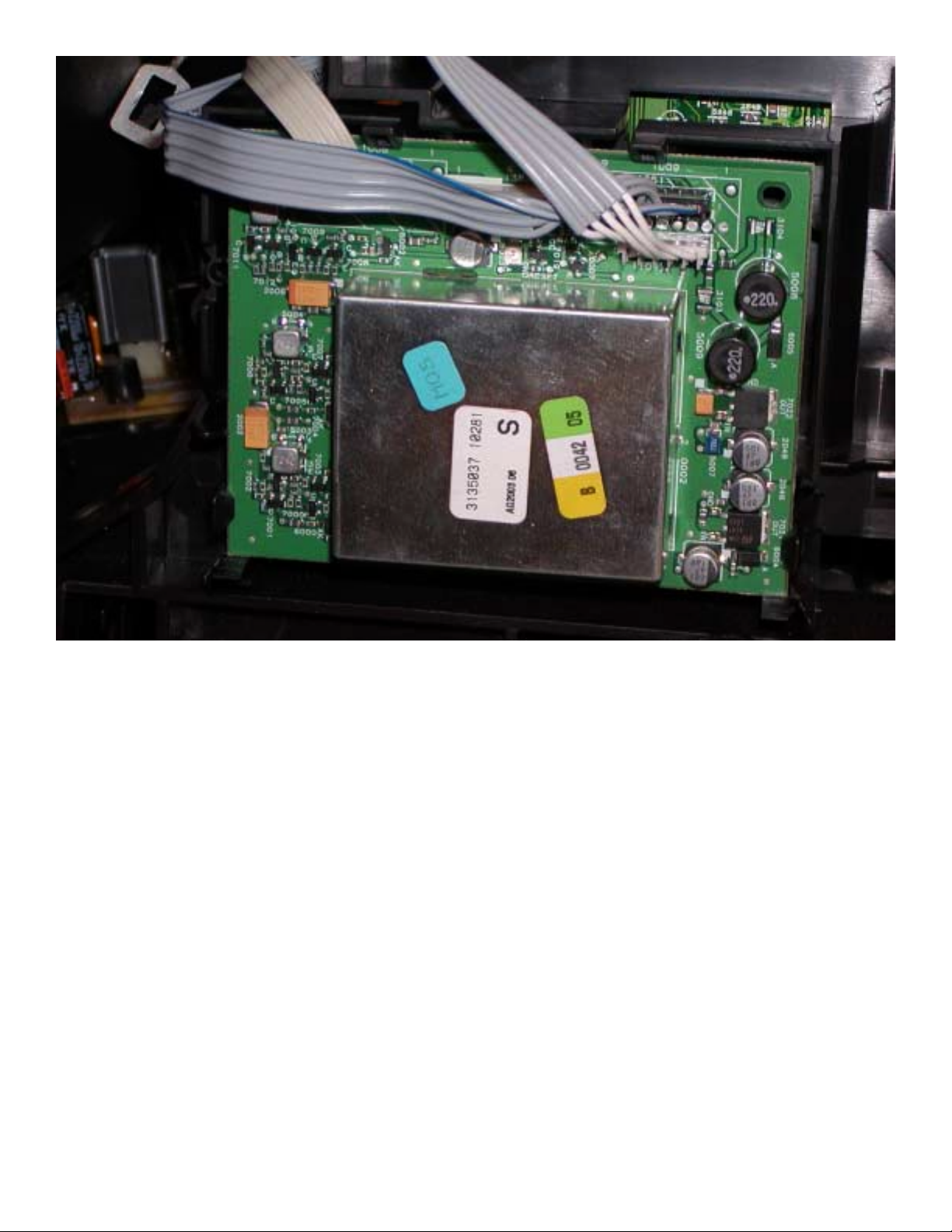
P8 Comb Filter Board
The tuner located on the LSP is referred to as the "Main Tuner". The tuner located on the PIP/DW
panel is referred to as the "PIP Tuner". Tuning is accomplished via IIC commands from the microprocessor (Painter) and AGC feedback from the HIP (High End Input Processor), both located on
the Small Signal Board (SSB).
The Main tuner contains a splitter, which splits the incoming RF signals between the Main and PIP
tuners.
To minimize interference, all channels chosen to be the "Main Picture" will be chosen via the IIC
bus, to be tuned in the "Main Tuner". Therefore, the "PIP Tuner" will always be tuned to the channel
selected to be the "PIP" picture.
Inputs from the "Main Tuner" are sent to connector 1205 (Sim Connector), pin 13 on the LSP and
are introduced into the SSB on pin 13 of connector 1000. Inputs from the "PIP Tuner" are
processed on the PIP/DW panel.
AV1, AV2, and AV3 inputs are routed to the SSB on pins 10, 1, 2, 3 - 6, 7 - 63, and 64, respectively. They are also routed to the PIP/DW panel via cable connectors, 1933 (pins 1, 2, and 3), 1935
(pins 1, 3, and 5), and 1935 (pins 1 and 2), respectively.
Page 8

AV4 inputs are matrixed (YPbPr to RGB) and Selected (Switched) on the HD Interface panel and
routed to the SSB via cable connector 1304 (pins 1, 2, and 3). Sync selection for AV4 inputs also
takes place on the HD Interface panel.
Signal selection and switching for AV1, AV2, AV3, and tuner inputs is performed on the SSB and
PIP/DW panel.
CVBS signals are routed through the SSB to the 3D Comb Filter board via connector 1303, pin 5.
The luminance and Chrominance are uniquely separated and are routed back through connector
1303, pins 1 and 3, to the SSB.
Y50, U50, and V50 signals (1fH) are sent from the SSB to the DW/PIP panel via connectors 1682
and 0205, respectively. H50 and V50 sync signals (1fH) are sent from the SSB to the PIP/DW panel
via connectors 1681,1948, 1937, and 0201, respectively, for the purpose of PIP window insertion.
Line doubling (1fH to 2fH conversion), YUV to RGB matrixing, Closed Caption generation, Picture
improvement, Video control, and Geometry geometry all take place on the SSB.
Video outputs from the SSB are routed to the CRT panel via connectors 1000, 1205 (Sim connector), and Cable connector 1940. Cutoff control is fed from the CRT panel to the SSB via the same
connectors.
Power Supply
The P8 chassis has two distinct power supplies. The Main power supply and the Standby power
supply.
The Main power supply is responsible for the generation of 141 volts, VBatt voltage and the (+) and
(-) 16 volt supplies used for the Audio circuits.
Page 9
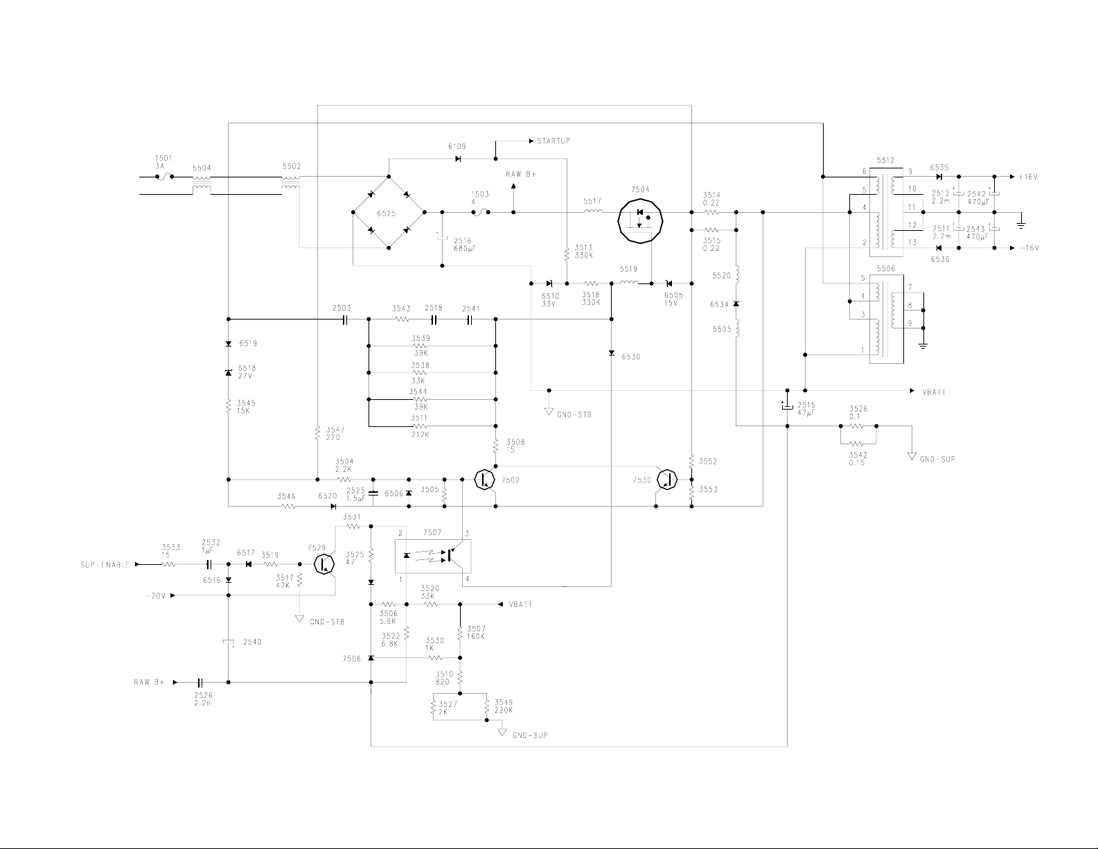
Figure 2 - Main Power Supply
Page 10
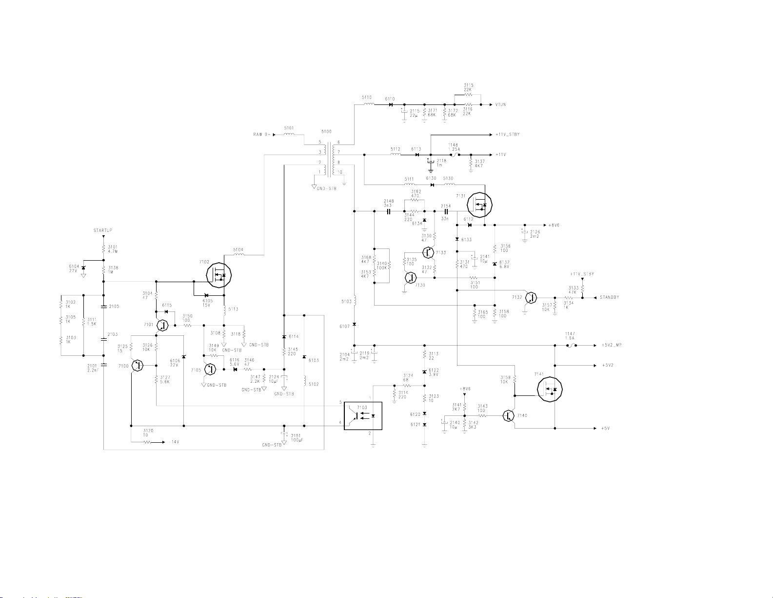
Figure 3 - Standby Power Supply
presently being manufactured. Therefore, we have no need to examine that circuitry in the P-8.
Lightning and surge protection are accomplished using the standard circuitry used in most sets
SUP, and two "COLD" (chassis) grounds, GND-SSP and GND-AUD. Caution: The two HOT
Grounds can Never be tied together. The two COLD grounds, although labeled differently, are both
common (chassis) grounds.
The Main power supply has four (4) separate grounds; two "HOT" grounds, GND-STB and GND-
Page 11

The Standby power supply is a Self-Oscillating power supply (SOPS). Regulation is accomplished by
utilizing the "flyback principle" to control the switching time of the oscillator circuit. Secondary regulation is accomplished by monitoring the 5.2 volt supply line. The changes felt on the 5.2 volt line are
coupled through an opto-coupler to the switching control circuitry in the primary side of the supply.
The Standby supply, as the name implies, delivers the 5.2 volt standby voltage to the control circuits
and also provides several operating voltages to the rest of the chassis. Two of the voltages supplying the chassis are switched (+8V6 and +5V) while the remaining supply voltages are present as
soon as the supply is energized (33 volt VTUN, +11V_STBY, +11V, +5V2_MP and +5V2).
The Standby supply, unlike the Main supply, utilizes two separate grounds; "hot" ground, GND-STB
and "cold" ground, CHASSIS. On schematic drawing A2, the chassis ground is labeled GND-SSP.
However, it is the same chassis ground that is utilized throughout the chassis.
Start-up
As soon as AC is applied to the chassis, it is rectified by bridge network, 6525 and diode 6109. This
provides a Raw B+ of approximately 143 volts and a Start-up voltage of approximately 60 volts.
The Raw B+ is applied to capacitor 2526, causing capacitor 2540 to begin charging. This produces
a negative voltage that is applied directly to the emitter of transistor 7529, turning it "on". With 7529
"on", the opto-isolator, 7507 turns "on". This turns transistor 7502 "on" effectively grounding the gate
of our switching transistor (FET), 7504. At this point in time, the Main supply is producing only two
voltages, Raw B+ and the Start-up voltage.
The Start-up voltage is felt on the gate of FET, 7102, in the Stand-by supply. This voltage is zenered
by diode, 6105, to approximately 15 volts, which is more than sufficient to turn 7102 "on". The flow
of current through 7102 creates a field in the primary winding (pins 3 & 5) of transformer 5100. This
field is also created in the co-coupled winding (pins 1 & 2). By the time the windings approach saturation, the voltage drop being felt by the current sensing resistors, 3108 & 3118, will have exceeded
1.4 volts. This is enough to turn transistor 7101 "on" which will effectively shut 7102 "off". This sudden cease of current flow will cause the fields to begin collapsing. This keeps 7102 turned "off" until
the fields have completely collapsed. At this time the voltage on the base of 7101 is insufficient to
maintain conduction and it shuts "off". This allows the Start-up voltage to once again, kick start 7102.
This cycling will continue until the circuit is stabilized. At that time, feedback from pin 2 of 5100,
through capacitor 2101 and it's associated RC network will sustain oscillation.
The changing fields in the primary winding of 5100 are inversely coupled to the secondary windings.
The secondary windings will provide our Stand-by and Operating voltages.
Five of the secondary voltages are unswitched and will be present as soon as the Stand-by supply
starts up. Two of the voltages are switched and will be present only after a command from the microprocessor. The five unswitched voltages are VTUN (33V), +11V_STBY, +11V, +5V2_MP, and +5V2.
On the primary side of the Stand-by supply, diode 6103 is rectifying the oscillator feedback pulses
creating the -20v DC voltage that will be sent to the Main supply and applied to the base and emitter
of transistor 7529. This voltage will keep 7529 "on", which keeps the Main supply turned "off".
Those same feedback pulses are being rectified by diode 6114 and the resultant DC voltage is being
applied to the anode of zener diode, 6116. If excessive voltage is sensed, 6116 will break down and
Page 12

transistor 7105 will turn "on", turning transistor 7101 "on", and turning 7102 "off".
Regulation in the Stand-by supply is accomplished by monitoring the 5.2 volt line via a voltage
divider network consisting of 3113, 6122, 3123, 6120, 6121, 3124, 3114 and an opto-isolator, 7103.
If the 5.2 volt source increases, the voltage drop across 3114 will increase. If the voltage across
3114 exceeds 1 volt, the diode portion of 7103 will conduct causing the transistor portion of 7103 to
conduct, passing a portion of the -20v DC voltage to the base of 7100. Transistor 7100 will now
allow a portion of the -20v to pass through (C to E) which will turn 7101 "on" and 7102 "off". Once
the 5.2 volt line settles back down to 5.2 volts, 7103 will cease conduction and the startup voltage
will trigger 7102 into oscillation again.
In the event of a failed opto-coupler, the secondary voltages will increase causing the primary voltages to also increase. An unregulated increase in the 5.2 volt supply could result in the destruction
of several IC's. Therefore, zener diode, 6106 will breakdown as soon as the negative voltage
exceeds -25 volts. By doing so, 6106 can assume regulation of the supply. This will limit the 5.2 volt
line to a maximum of 6.5 volts which will prevent any damage to the IC's being fed by that line.
Note: We are still operating in the Stand-by mode (no "power on" command has been issued).
As soon as the 5V2 voltage comes up in the Standby supply, the microprocessor receives a reset
pulse on pin 73. This "reset" serves to "wake-up" the microprocessor. The microprocessor will now
be able to receive commands and communicate with other IC's.
Power-On"
When the 'power-on" command is received, either from the remote transmitter or the customer control panel, several things happen almost simultaneously:
The microprocessor will bring the base of 7132 "low", shutting it off. This will allow 7131 and 7141 to
turn "on", energizing the +8V6 and the +5V supplies.
As soon as the microprocessor confirms that the two supplies are energized and correct, it will issue
a command to the HOP IC to begin outputting a "soft-start" horizontal drive signal. Using the "softstart" method of horizontal stabilization, this process takes approximately 150msec.
Page 13
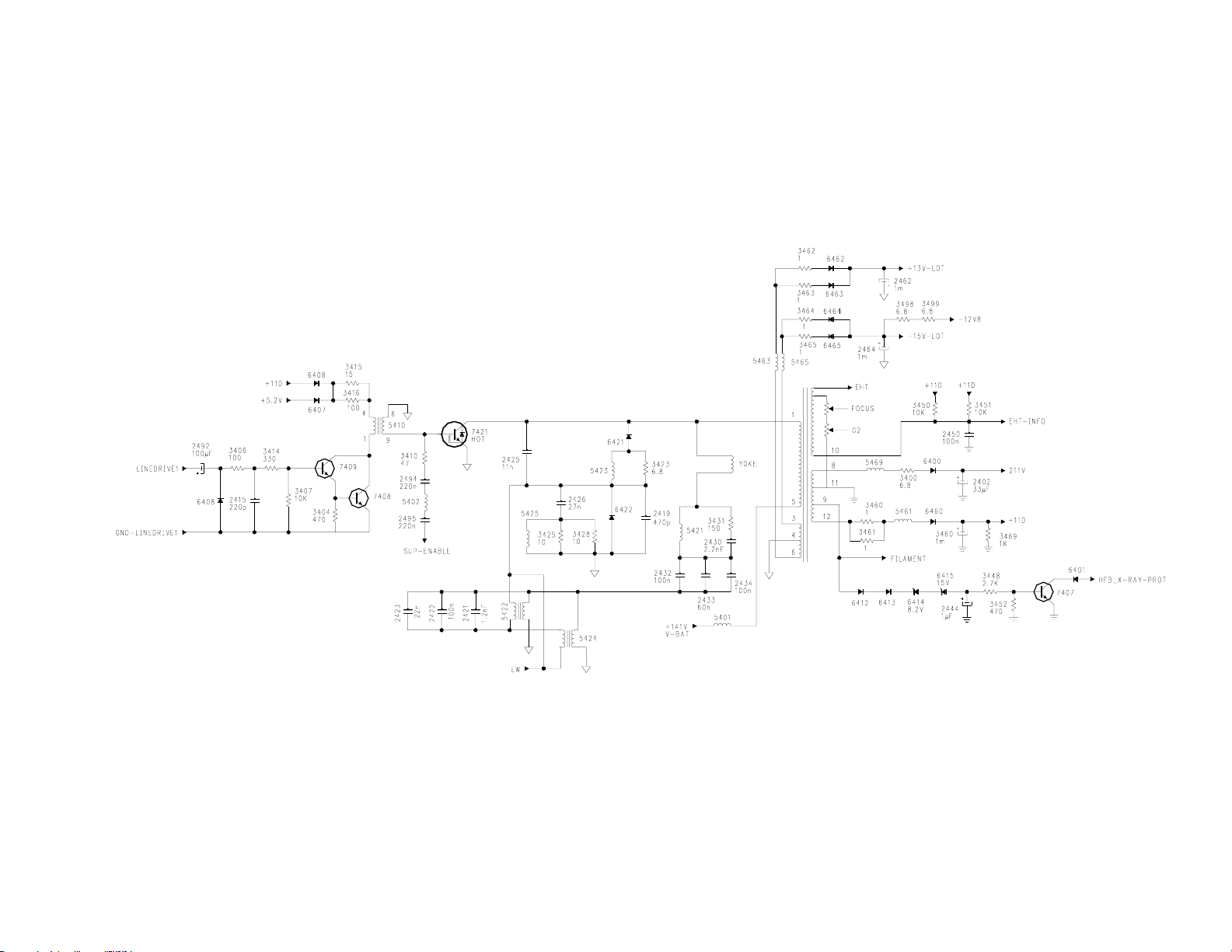
Figure 4 - Horizontal Deflection
Page 14

The horizontal pulses appear at the base of the Horizontal Output transistor, 7421. The pulses
meant to drive the horizontal output stage are also used for another purpose. They are coupled
through 3410, 2494, 5402, and 2495 to create the SUP_ENABLE circuit.
Those pulses are now applied to 3533 in the Main power supply. The negative peaks are rectified,
smoothed, and the resultant -DC voltage is applied to the base of 7529. This turns 7529 "off", 7507
"off", and 7502 "off".
The STARTUP voltage being rectified by 6109 is now allowed to "Kick-start" 7504 in the Main supply. 7504 saturates causing a large increase of current through the circuit. This causes a field to
build up in the primary winding of 5512 (pins 4 and 2) and co-coupled winding (pins 3 and 1). The
build up of current is felt across resistors 3514 and 3515. By the time the field is at maximum
strength, the voltage drop across 3514 and 3515 is sufficient to turn 7530 "on", bringing the gate of
7504 to ground. 7504 will shut "off" and the field built up in the primary windings will begin to collapse. When the field has collapsed, 7530 will lose it's bias and shut "off" allowing the gate of 7504
to become kick-started again. This procedure will continue until oscillation stabilizes. At that point,
oscillation is sustained by a feedback circuit consisting of 2503 and it's associated circuitry.
The changing fields in the primary windings are coupled to the secondary winding to create our (+)
and (-) 16 volt Audio supplies.
The primary winding consisting of pins 3 and 1, in conjunction with diode 6534 and capacitor 2515
develops our VBatt (141V) voltage.
Developing VBatt
In order to completely understand the uniqueness of this power supply, it is best to look at it as 2
separate supplies. The first supply will consist of the bridge (which develops raw B+ and Start-up
voltage) and a switch, 7504 that supplies a path for current flow through the primary windings of
5512 and 5506. Simply stated, the components mentioned, act as a "source" for the build up of the
fields in the primary windings.
The second supply will become active after 7504 is switched "off" and the fields begin collapsing; will
primarily consist of the primary windings, 6534, and 2515. This can be considered the supply for VBatt.
When 7504 is switched "on", current flow will be from GNDSTB, through the windings, through 7504,
and into the bridge. This creates a positive polarity on pin 1 of 5506 and pin 4 of 5512.
When 7504 is switched "off", the fields in the primaries change polarity and begin collapsing. Current
will now flow through 6534, charge 2515, flow through 3526/3542 to GNDSUP. At this time, the
Horizontal Output transistor, 7421, is being turned "on" by the horizontal drive pulse (being applied to
the base). 7421 utilizes GNDSUP, which will supply a path for our current to flow through 7421; it's
associated circuitry, the flyback transformer, back to the power supply via the VBatt line. The most
important item to remember is there are two different grounds in this portion of the Main supply.
Page 15

Primary Regulation
Regulation is accomplished by monitoring the 141V VBatt supply. Changes in the VBatt voltage are
felt across a voltage divider network consisting of 3507, 3510, 3527/3549, and 3530. If the voltage
applied to the programmable regulator, 7506, by 3530 exceeds 1 volt, 7506 will conduct and turn
7507 "on". This will turn 7502 "on" and bring the gate of 7504 to ground, shutting it "off". This cycle
will continue until the "off" time of 7504 is sufficient to lower VBatt to 141 volts.
A rapid increase in line voltage or an unusual increase in primary current will also be felt across
3514 and 3515. The resultant voltage will be fed through 3547 and 3504, added to the threshold
voltage sitting on pin 3 of 7507, and applied to the base of 7502. This will turn 7502 "on" and shut
7504 "off". This action occurs much faster than the correction provided by 7530 during the start-up
sequence due to the threshold voltage from 7507, which is already present at the base of 7502.
Once again, strict attention should be given to the Two Different Grounds.
P8
Troubleshooting Hints
Checking the operation of the Main Supply without the Horizontal Output transistor connected
This power supply requires a load at all times. Prior to testing, the horizontal output transistor
should be removed and a 100 watt light bulb should be inserted between VBatt and GND-SUP. The
positive terminal of Capacitor 2515 is a good location for one of the connections. The second connection can easily be made at the solder pad (vacated by the horizontal output transistor) labeled E
(emitter). The light bulb will now act as a load for the 141 VBatt supply.
Short the base to emitter of transistor 7529 and apply AC power. Two things should occur: The 141
volts should appear on the positive terminal of Capacitor 2515 and the light bulb should burn brightly.
This indicates the Main supply is functioning and regulating.
Checking the Stand-by supply for the switched +8.6V and +5V supplies
Assuming all unswitched secondary supplies are present, the two switched supplies can be checked
in the following manner: Short the base to emitter on transistor 7132 and measure the voltage
appearing on the source legs of FET's 7131 and 7141. There should be +8.6V on the source of
7131 and +5V on the source of 7141. If both voltages fail to appear, suspect 7132. If only one of the
voltages appear, troubleshoot the missing voltage source.
Unable to turn the set on
After confirming operation of the power supplies, the first check to be made is to see if the base of
7132 goes low (0) when the power button is pushed. If it does, the microprocessor is working. If it
does not, without pushing the power button, check for approximately 3.3 volts on pins 3 and 7 of
connector 0241 on the Front Keyboard assembly. If this voltage is missing, suspect a problem on
the SSB, related to the 3.3 volt supply to the microprocessor.
Page 16

Deflection Circuits
(Refer to Schematic Drawing B2)
The Horizontal and Vertical Sync pulses are developed in the HIP IC, 7323. The CVBS (Video) signal is fed to the Sync Block where it provides a reference for synchronization of the H and V Sync
signals which are output on pins 60 and 61. From pins 60 and 61 on the HIP IC, the sync pulses are
routed directly to pins 28 and 29 of the PICNIC IC, 7709 and to pins 94 and 70 of the Double
Window Signal Processor IC, 7801.
(Refer to Schematic Drawing C1)
The reason for routing the H and V sync pulses to 7801 is to allow syncronization of the PIP
Window or Dual Window PIP (window) with the Main Video signal when inserted. Synchronization
for the PIP picture (inside the PIP window) will come from the Dual Window circuitry.
(Refer to Schematic Drawing B3)
Once processed by the PICNIC IC, 7709, the sync signals are doubled in frequency inside the PROZONIC IC, 7706 which accomplishes this doubling by utilizing the two field memory ICs, 7714 and
7715. The sync signals are now fed back into the PICNIC. The Horizontal sync is now 31.468 Khz.
In the case of NTSC signals, the Vertical sync will be 60 Hz (there is no benefit to doubling the vertical) because 60 Hz is above detection of the human eye. In a case where the Main video signal is
missing, the HIP IC will not output signals to 7709. The sync pulses will be generated within 7709 to
allow for a stable OSD. The processed sync pulses will exit 7709 on pins 18 and 19 and are routed
to pins 24 and 23 of the HOP IC, 7301.
(Refer to Schematic Diagram B4)
The HOP IC will now generate our Horizontal and Vertical drive pulses. The Horizontal drive pulses
exit 7301 on pin 8 and are routed through pin 26 of connector 1000. The Horizontal drive (Line
drive) ground circuit is connected to pin 27 of connector 1000.
The Horizontal drive signal starts at approximately 50 kHz with a very short "on" time. The "on" time
is gradually increased until the frequency stabilizes at 31.468 kHz. The time involved for this procedure is approximately 150 msec. This is referred to as a "Soft Start" and is sometimes used to protect CRT's with Dynamic Astigmatic Focus (DAF) guns.
From connector 1000, the drive pulse is coupled to the base of 7409. Whenever the base goes positive, transistors 7409 and 7408 will conduct. This will cause increasing and decreasing current to
flow through transformer 5410. The fluctuating current in the primary creates a fluctuating field that
is coupled to the secondary via transformer action. This transformer action places our drive signal
on the base of the Horizontal Output transistor, 7421. CAUTION: Once our signal reaches the secondary winding of 5410, "HOT GROUND" must be used as a reference. It is necessary to insure the
"Hot Ground you choose is labeled "GND-SUP". Safety precautions used while working in the power
supply apply in this circuit.
The drive signal now has two paths to follow. The first path is through 3410, 2494, 5402 and 2495
back to the Main Supply. This path is explained in the section on "Power Supply".
Page 17

The second path is through the Horizontal Output transistor, 7421. The drive signal is amplified by
7421, shaped by capacitors 2418, 2425, 2426 and 2419. The result of this amplification and shaping
is a large clean positive pulse. The output pulse is applied to the Line Deflection Yoke and the
Flyback transformer.
Before we examine what the secondary side of 5430 is doing while being driven by the Horizontal
Output signal, we should look at the East West Drive circuitry. This circuitry provides an increase or
decrease in deflection current, depending where the actual beam is during the scan.
(Refer to Schematic Diagram B4) (Not shown here)
The East West Correction signal originates in the HOP IC, 7301. The E/W Drive signal is developed
in the deflection block of 7301. It is dependent on input from the Internal Vertical generation and
External EHT-INFO circuitry. The EHT-INFO circuit will be covered under secondary voltages of 5430.
During the scan process, the beam travels slower in the center of the screen than it does at the
sides. Therefore, we must have a method of increasing deflection current as the beam approaches
the center of the screen. If we do not compensate for this, a line in the center will be larger than at
it's edges. To accomplish this, the HOP IC mixes a parabolic waveform (with negative peaks) from
the internal ramp generator with input from the EHT-INFO line (pin 4) and outputs a composite of the
two on pin 3. The EHT-INFO line decreases when the beam current increases. This information is
used to compensate for picture size.
(Drawing Not Available at the time of printing)
(Refer to Schematic Diagram A4)
This signal is routed to 7450-B where it is amplified and used to drive Opto-coupler, 7482. This
device uses two grounds. The diode portion uses chassis ground and the transistor portion uses
HOT ground as a reference. The voltage variations from pin 4 of 7482 are applied to 7487, amplified, inverted, applied to 7486, again amplified, inverted and applied to the gate of 7480. The signal
variations are used to switch 7480 on and off at the necessary rate to provide any required corrections. There are two outputs that are utilized from the switching of 7480. The signal felt on the
source is routed to the protection circuits. The signal felt on the drain is routed to the Line Output circuit (Horizontal Output Stage) and to additional protection circuits. The protection circuits will be covered as a separate subject. The previous statements can be more readily understood by observing
the Power/Deflection Block diagram in Manual 7622.
(Drawing Not Available at time of printing)
(Refer to Schematic Drawing A3)
The E/W switching FET, 7480, will charge capacitor 2421 until it reaches saturation. This will occur
during the flyback period. The moment 7480 saturates, 2421 will discharge. When the scan begins
again, 2421 will charge via conduction diode 6422. Charging will continue via 6422 until the voltage
on 2421 is equal to the voltage across 5422. During the scan period, 2421 charges, allowing more
current to flow through the Yoke Coil and less current to flow through 5422. This creates an increase
in picture width. Conversly, if the E/W drive signal causes 7480 to shut off, the current flow through
the Yoke coil will be less than the current flow through 5422 and the picture width will decrease.
(Drawing not available at time of printing
Page 18

There are two more correction circuits on the primary side of the flyback. The first one is "Linearity
Correction". Because there is inherent resistance in the deflection coil, another coil is added which
helps ensure a more linear sawtooth waveform. The new coil is 5421 and is referred to as the linearity coil. Capacitors 2430 and 2431, in series with resistor 3431 prevent self oscillation of 5421.
The second correction circuit is formed by the addition of capacitor 2433 which provides "S" correction. Because the sides of the picture are further away from the point of deflection than the center,
2433 is added to decrease the deflection current at the left and right edges of the scan. The saw
tooth current will generate a parabolic voltage with negative voltage peaks. This voltage is also felt
across 2421 resulting in a proportional increase in picture width. The E/W drive signal will ensure the
largest picture width in the center of the frame and maximum deflection current will flow through
2433 at this time.
Having observed the primary side of 5430, we will now observe the secondary side. Through normal
transformer action, the collapsing fields on the primary windings are induced into the secondary
windings.
The secondary windings consisting of pins 3 to 4 and 6 to 4 (4 being "hot" ground) are the only two
secondary supplies using "Hot Ground" (GND-SUP) as a reference. The pulses on each of these
lines create the two voltages for our Vertical (Frame) Deflection circuitry which also uses "Hot
Ground" for a reference. The voltages developed for use on the CRT or the CRT board are: EHT
(high voltage), Focus voltage, G2 (screen voltage), 211 volt (Video B+) and Filament voltage.
Two additional voltages are derived from the secondary windings. EHTinfo and the +11D supply.
EHTinfo is a DC average of the unrectified pulses coming from pin 10 which are felt across a voltage divider network consisting of 3450, 3451 and 2450. The +11D supply is used in the cold ground
sections of our deflection circuits.
EHTinfo is applied to the HOP IC on pins 43, 4, 5 and in the form of Phase correction, pin 14
(Actually derived from EHTinfo line). The end result of these applications is contrast control, width
control, E/W current correction and Dynamic Phase Correction which controls the "on" time of the
Horizontal Output transistor, 7421, to reduce excessive beam current.
The final secondary output is the HFB_X-RAY-PROT. This output is derived from the average DC
voltage created by pin 9 of 5430 which is the filament line to the CRT. If the average DC voltage
increases beyond a trigger point, transistor 7407 will turn "On". This will be felt at two separate locations on the HOP IC. The first location is through 3324 to pin 13. This will shut down the horizontal
drive. The second location is to the base of 7317 which, ultimately will place a positive voltage on
pin 4, shutting down the EW drive and the Vertical drive.
We have just completed our examination of the Horizontal drive and output circuits. We will now
examine the Vertical circuits.
The VD100 sync pulse enters the HOP IC, 7301, on pin 23 and internally sent to the Ramp
Generator Block. From there, the ramp enters the Frame Block where it is processed and output on
pins 1 & 2 as Frame Drive(+) and Frame Drive(-). A third element is added to our vertical pulses;
The DC rotation voltage is superimposed on the Frame Drive+ line. This eliminates the need for
three lines to the vertical circuit. The DC rotation voltage is used to enhance the control of the vertical height and tilt. It is designed to coincide with minor changes in line frequency and is active only
in wide screen versions.
Page 19

In the process of routing our drives from the HOP IC to the vertical circuit, it is necessary to provide
for two separate grounds. In order to do this, two methods are used. Transformer isolation and optocoupling. Both methods use "cold ground" on the input side and "hot" ground on the output side. Our
drive signal is isolated and transformer coupled by 5621, to the base of 7611 where it is amplified
and routed to 7612 for further amplification. From there, it is sent to pins 7 and 1 of the Vertical
Output IC, 7620.
7620 has two supply voltages. The +13Vlot and the -15Vlot, both derived from the secondary side of
the flyback transformer. 7620 will shape and amplify our vertical drive pulse. The output waveform will
exit 7620 on pin 5 and be used to drive the vertical deflection yoke. Feedback to 7620 will be via 3623.
If there is a loss of vertical output pulses, 7641 will turn "off". This will allow 2642 to charge up and
turn 7443 "on". The result would be the grounding of the SUP_Enable line, which would be felt on
the base of 7529 in the Main supply, causing the supply to shutdown.
Audio Signal Paths
The Audio Signal paths are the same as the paths in the R8 and several chassis in the PTV family.
Page 20

JL 03/03/04
 Loading...