

Philips P87C055BBP, P83C845BBP, P83C055BBP Datasheet

INTEGRATED CIRCUITS
DATA SH EET
83C145; 83C845
83C055; 87C055
Microcontrollers for TV and video
(MTV)
Product specification
File under Integrated Circuits, IC20
1996 Mar 22

Philips Semiconductors Product specification
Microcontrollers for TV and video (MTV)
CONTENTS
1 FEATURES
2 DESCRIPTION
3 APPLICATIONS
4 ORDERING INFORMATION
5 BLOCK DIAGRAM
5.1 Part options
6 PINNING INFORMATION
6.1 Pinning
6.2 Pin description
7 DESCRIPTION OF STANDARD FUNCTIONS
8 INPUT/OUTPUT (I/O)
9 DESCRIPTION OF DERIVATIVE
FUNCTIONS
9.1 General description
10 6-BIT PWM DACS
10.1 PWM DAC operation
10.2 Special Function Register PWMn (n = 0 to 7)
11 14-BIT PWM DAC (TDAC)
11.1 14-bit counter
11.2 14-bit DAC operation
11.3 Special Function Register TDACL
11.4 Special Function Register TDACH
12 SOFTWARE ANALOG-TO-DIGITAL FACILITY
12.1 Special Function Register SAD
12.2 Software ADC operation
13 ON SCREEN DISPLAY (OSD)
13.1 OSD features
13.2 General description of the OSD module
13.3 OSD logic
13.4 Character Generator ROM
13.5 Display RAM organization
13.6 OSD Special Function Registers
13.7 OSD Control Register OSCON
13.8 OSD Control Register OSMOD
13.9 OSD Control Register OSORG
83C145; 83C845
83C055; 87C055
14 PROGRAMMING CONSIDERATIONS
14.1 EPROM Characteristics
14.2 Programming operation
14.3 Erasure Characteristics
14.4 Reading Signature Bytes
14.5 EPROM Programming and Verification
15 PROGRAMMING THE OSD EPROM
15.1 Overview
15.2 Character description and programming
15.3 OSD EPROM bit map
16 REGISTER MAP
17 LIMITING VALUES
18 HANDLING
19 DC CHARACTERISTICS
20 AC CHARACTERISTICS
21 PACKAGE OUTLINES
22 SOLDERING
22.1 Introduction
22.2 Soldering by dip or wave
22.3 Repairing soldered joints
23 DEFINITIONS
24 LIFE SUPPORT APPLICATIONS
1996 Mar 22 2

Philips Semiconductors Product specification
Microcontrollers for TV and video (MTV)
1 FEATURES
• Masked ROM sizes:
– 8 kbytes (83C845)
– 12 kbytes (83C145)
– 16 kbytes (83C055)
– 16 kbytes OTP (87C055)
• RAM: 256 bytes
• On Screen Display (OSD) controller
• Three digital video outputs
• Multiplexer/mixer and background intensity controls
• Flexible formatting with OSD New Line option
• 128 × 10 bits display RAM
• Designed for reduced Radio Frequency Interference
(RFI)
• Character generator ROM:
– character format 18 lines × 14 dots
– 60 visible characters
– 4 special characters
• Eight text shadowing modes
• Text colour selectable per character
• Background colour selectable per word
• Background colour versus video selectable per
character
• Eight 6-bit Pulse Width Modulators (PWM) for analog
voltage integration
83C145; 83C845
83C055; 87C055
• One 14-bit PWM for high-precision voltage integration
• Digital-to-analog converter and comparator with 3 inputs
multiplexer
• Nine dedicated I/Os plus 28 port bits (15 port bits with
alternative uses)
• 4 high current open-drain port outputs
• 12 high voltage (+12 V) open-drain outputs
• Programmable video input and output polarities
• 80C51 instruction set
• No external memory capability
• Plastic shrink dual in-line package (0.07 inch centre
pins)
• High-speed CMOS technology
• Power supply: 5 V ±10%.
2 DESCRIPTION
The 83C055, Microcontroller for Television and Video
(MTV) applications, is a derivative of Philips’ industry
standard 80C51 microcontroller.
The 83C055 is intended for use as the central control
mechanism in a television receiver or tuner.
3 APPLICATIONS
Providing tuner functions and an OSD facility, it represents
a next generation replacement for the currently available
parts.
4 ORDERING INFORMATION
PACKAGE TEMP.
TYPE NUMBER
P83C055BBP
P87C055BBP
P83C145BBP
P83C845BBP
1996 Mar 22 3
NAME DESCRIPTION VERSION
SDIP42 plastic shrink dual in-line package; 42 leads (600 mil) SOT270-1 0 to +70 3.5 to 12
RANGE
(°C)
FREQ.
(MHz)

Philips Semiconductors Product specification
Microcontrollers for TV and video (MTV)
5 BLOCK DIAGRAM
handbook, full pagewidth
V
DD
XTAL1
(IN)
XTAL2
(OUT)
RST
T0
8-BIT
TIMER /
EVENT
COUNTER
80C51
core
excluding
ROM / RAM
CPU
INT0INT1
ROM
(1)
PARALLEL
I / O
PORTS
RAM
256 bytes
8 x 6-BIT PWM
VID1
BF
VID2
DISPLAY
RAM
128 × 10
VCTRL
VID0
VCLK2
OSD BLOCK
14-BIT
PWM
83C145; 83C845
83C055; 87C055
VCLK1
CHARACTER
GENERATOR
60 × 18 × 14
8-bit internal bus
HSYNC
VSYNC
ROM
SOFTWARE
CONTROL
ADC
V
SS
8884
P3 P2 P1
(1) ROM sizes: see Table 1.
8
PWM0 to PWM7
P0
TDAC
3
ADI2 to ADI0
MBE766
Fig.1 Block diagram.
5.1 Part options
Table 1 Differences between the types
TYPES
MEMORY
83C845 83C145 83C055 87C055
ROM 8 kbytes 12 kbytes 16 kbytes −
EPROM (OTP) −−−16 kbytes
1996 Mar 22 4

Philips Semiconductors Product specification
Microcontrollers for TV and video (MTV)
6 PINNING INFORMATION
6.1 Pinning
handbook, halfpage
VPP/TDAC/P0.0
handbook, halfpage
PROG/PWM1/P0.1
ASEL/PWM2/P0.2
PWM3/P0.3
PWM4/P0.4
PWM5/P0.5
PWM6/P0.6
PWM7/P0.7
ADI0/P1.0
ADI1/P1.1
ADI2/P1.2
PWM0/P1.3
P2.7
P2.6
P2.5
P2.4
P2.3
P2.2
P2.1
P2.0
V
SS
1
2
3
4
5
6
7
8
9
10
11
12
13
14
15
16
17
18
19
20
83C145
83C845
83C055
87C055
MBE765
42
41
40
39
38
37
36
35
34
33
32
31
30
29
28
27
26
25
24
23
2221
V
DD
P3.7
P3.6
P3.5
P3.4
P3.3/INT0
P3.2/T0
P3.1/INT1
P3.0
RST
XTAL2
XTAL1
BF
VCLK2
VCLK1
VSYNC
HSYNC
VCTRL
VID2
VID1
VID0
83C145; 83C845
83C055; 87C055
Fig.2 Pin configuration (SOT270-1).
1996 Mar 22 5

Philips Semiconductors Product specification
Microcontrollers for TV and video (MTV)
83C145; 83C845
83C055; 87C055
6.2 Pin description
Table 2 Pin description SDIP42 (SOT270-1)
SYMBOL PIN DESCRIPTION
Port 0 (notes 1, 2 and 4)
P0.0/TDAC/V
P0.1/PWM1/PROG 2 P0.1: open-drain bidirectional port line;
P0.2/PWM2/ASEL 3 P0.2: open-drain bidirectional port line;
P0.3/PWM3
to
P0.7/PWM7
Port 1 (notes 1, 2 and 5)
P1.0/ADI0
to
P1.2/ADI2
P1.3/PWM0 12 P1.3: open-drain bidirectional port line; PWM0: output for the 6-bit lower-precision
PP
1 P0.0: open-drain bidirectional port line;
TDAC: output for the 14-bit high-precision PWM;
VPP: 12 V programming supply voltage during EPROM programming.
PWM1: output for the 6-bit lower-precision PWM;
PROG: input for EPROM programming pulses.
PWM2: output for the 6-bit lower-precision PWM;
ASEL: input indicating the EPROM address bits that are applied to Port 2.
4to8 P0.3 to P0.7: 5 open-drain bidirectional port lines;
PWM3 to PWM7: 5 outputs for the 6-bit lower-precision PWM.
9to11 P1.0 to P1.2: 3 open-drain bidirectional port lines;
ADI0 to ADI2: inputs for the software analog-to-digital facility.
PWM. PWM0 can be externally pulled up as high as +12 V ±5%
Port 2
P2.7 to P2.0 13 to 20 Port 2: 8-bit open-drain bidirectional port; P2.3 to P2.0 have high current capability
(10 mA at 0.5 V) for driving LEDs. Port 2 pins that have logic 1s written to them float,
and in that state can be used as high-impedance inputs. Any of the Port 2 pins are
driven LOW if the port register bit is written as a logic 0. The state of the pin can
always be read from the port register by the program.
Port 3 (note 1 and 3)
P3.0 34 P3.0: open-drain bidirectional port line.
P3.1/INT1 35 P3.1: open-drain bidirectional port line; INT1: External interrupt 1.
P3.2/T0 36 P3.2: open-drain bidirectional port line; T0: Timer 0 external input.
P3.3/INT0 37 P3.3: open-drain bidirectional port line; INT0: External interrupt 0.
P3.4 to P3.7 38 to 41 P3.4 to P3.7: 4 open-drain bidirectional port lines.
General
V
SS
VID2 to VID0 22 to 24 Digital Video bus: Three totem-pole outputs comprising digital RGB (or other colour
VCTRL 25 Video Control: A totem-pole output indicating whether the OSD facility is currently
21 Ground: 0 V reference.
encoding) from the OSD facility. The polarity of these outputs is controlled by a
programmable register bit (register OSCON; bit Po).
presenting active video on the VID2 to VID0 outputs. Signal is used to control an
external multiplexer (mixer) between normal video and the video derived from VID2 to
VID0. The polarity of this output is controlled by a programmable register bit (register
OSCON; bit Pc).
1996 Mar 22 6

Philips Semiconductors Product specification
Microcontrollers for TV and video (MTV)
83C145; 83C845
83C055; 87C055
SYMBOL PIN DESCRIPTION
HSYNC 26 Horizontal Sync: A dedicated input for a TTL-level version of the horizontal sync
pulse. The polarity of this pulse is programmable; its trailing edge is used by the OSD
facility as the reference for horizontal positioning.
VSYNC 27 Vertical Sync: A dedicated input for a TTL-level version of the vertical sync pulse. The
polarity of this pulse is programmable, and either edge can serve as the reference for
vertical timing.
VCLK1 28 VCLK1: Video Clock 1; input for the horizontal timing reference for the OSD facility.
VCLK2 29
BF 30 Background/Foreground: A totem-pole output which, when VCTRL is active,
XTAL1 31 XTAL1: Input to the inverting (oscillator) amplifier and clock generator circuit that
XTAL2 32
RST 33 Reset: If this pin is HIGH for two machine cycles (24 oscillator periods) while the
V
DD
Notes
1. Port 0, Port 1 , and Port 3 pins that have logic 1s written to them float, and in that state can be used as
high-impedance inputs.
2. The state of the pin can always be read from the port register by the program.
3. P3.0, P3.4, and P3.7 can be externally pulled up as high as +12 V ±5%; while P3.5 and P3.6 have 10 mA drive
capability.
4. For each PWM block, a register bit (register PWMn; bit PWnE; n = 0 to 7) controls whether the corresponding pin is
controlled by the block or by Port 0; Port 0 controls the pin immediately after a reset. Regardless of how each pin is
controlled, it can be externally pulled up as high as +12 V ±5%.
5. Any of the Port 1 pins are driven LOW if the corresponding port register bit is written as a logic 0, or for P1.3 only, if
the TDAC module presents a logic 0.
VCLK2: Video Clock 2; output from the on-chip video oscillator. VCLK1 and VCLK2
are intended to be used with an external LC circuit to provide an on-chip oscillator. The
period of the video clock is determined such that the width of a pixel in the OSD is
equal to the inter-line separation of the raster.
indicates whether the current video data represents a Foreground (LOW) or
Background (HIGH) dot in a character. This signal can be used to reduce the intensity
of the background colour and thus emphasize the text.
provides the timing reference for all 83C055 logic other than the OSD facility.
XTAL2: Oscillator output terminal for system clock. XTAL1 and XTAL2 can be used
with a quartz crystal or ceramic resonator to provide an on-chip oscillator. Alternatively,
XTAL1 can be connected to an external clock, and XTAL2 left unconnected.
oscillator is running, the MTV is reset. This pin is also used as a serial input to enter a
test or EPROM programming mode, as on the 87C751.
42 Power supply: for normal and Power-down operation.
1996 Mar 22 7

Philips Semiconductors Product specification
Microcontrollers for TV and video (MTV)
7 DESCRIPTION OF STANDARD FUNCTIONS
For a description of the standard functions please refer to
the
“Data Handbook IC20; Section 2: 80C51 Technical
Description”
8 INPUT/OUTPUT (I/O)
The I/O structure of the 83C055 is similar to the standard
I/O structure in the 80C51, except for the points described
in Table 5.
9 DESCRIPTION OF DERIVATIVE FUNCTIONS
9.1 General description
Although the 83C055 is specifically referred to throughout
this data sheet, the information applies to all the devices.
The differences to 80C51 features and the derivative
functions are described in the following Sections and
Chapters.
Figure 1 shows the block diagram of the 83C055.
9.1.1 N
Standard functions to the 80C51 that are not implemented
in the 83C055:
• As Data and Program Memory are not externally
expandable on the 83C055, the ALE, EA, and
PSEN signals are not implemented.
• Idle mode.
• Power-down mode.
.
OT IMPLEMENTED FUNCTIONS
83C145; 83C845
83C055; 87C055
• The IP register is not used, and the IE register (address
A8H) is similar to that on the 80C51;see Table 36.
• The VSYNC input used by the OSD facility can generate
an interrupt. The active polarity of the pulse is
programmable (see Section 13.7); interrupt occurs at
the leading edge of the pulse.
• Since there is no serial port, there are no interrupts nor
control bits relating to this interrupt. The interrupts and
their vector addresses are shown in Table 3.
• External Interrupt 1 is modified so that an interrupt is
generated when the input switches are in either direction
(on the 80C51, there is a programmable choice between
interrupt on a negative edge or a LOW level on INT1).
This facility allows for software pulse-width
measurement handling of a remote control.
Table 3 Program Memory address
EVENT PROGRAM MEMORY ADDRESS
Reset 000H
External INT0 003H
Timer 0 00BH
External INT1 013H
Timer 1 01BH
VSync Start 023H
9.1.3 PCON REGISTER DIFFERENCE
The PCON register format is shown in Table 4. Bits GF1
and GF0 are general purpose flag bits.
9.1.2 I
The interrupt facilities of the 83C055 differ from those of
the 80C51 as follows:
9.1.4 I/O PORTS DIFFERENCES
Table 5 I/O ports differences
Port 0 external memory expansion 8-bit open-drain bidirectional port; and includes:
Port 1 8-bit general purpose quasi-bidirectional 4-bit open-drain port, and includes alternative uses
Port 2 quasi-bidirectional and can be used for external
Port 3 quasi-bidirectional; all eight bits have alternate uses 3 port bits have some of the same alternative uses
1996 Mar 22 8
NTERRUPT FACILITIES DIFFERENCES
I/O STANDARD 80C51 83C055
memory expansion
Table 4 PCON Register format (address 87H)
76543210
−−−−GF1 GF0 −−
alternative use for PWM outputs
for analog inputs and a PWM output
open-drain and general purpose
as on the 80C51 but not necessarily on the same
pins; 5 pins are open-drain and general purpose

Philips Semiconductors Product specification
Microcontrollers for TV and video (MTV)
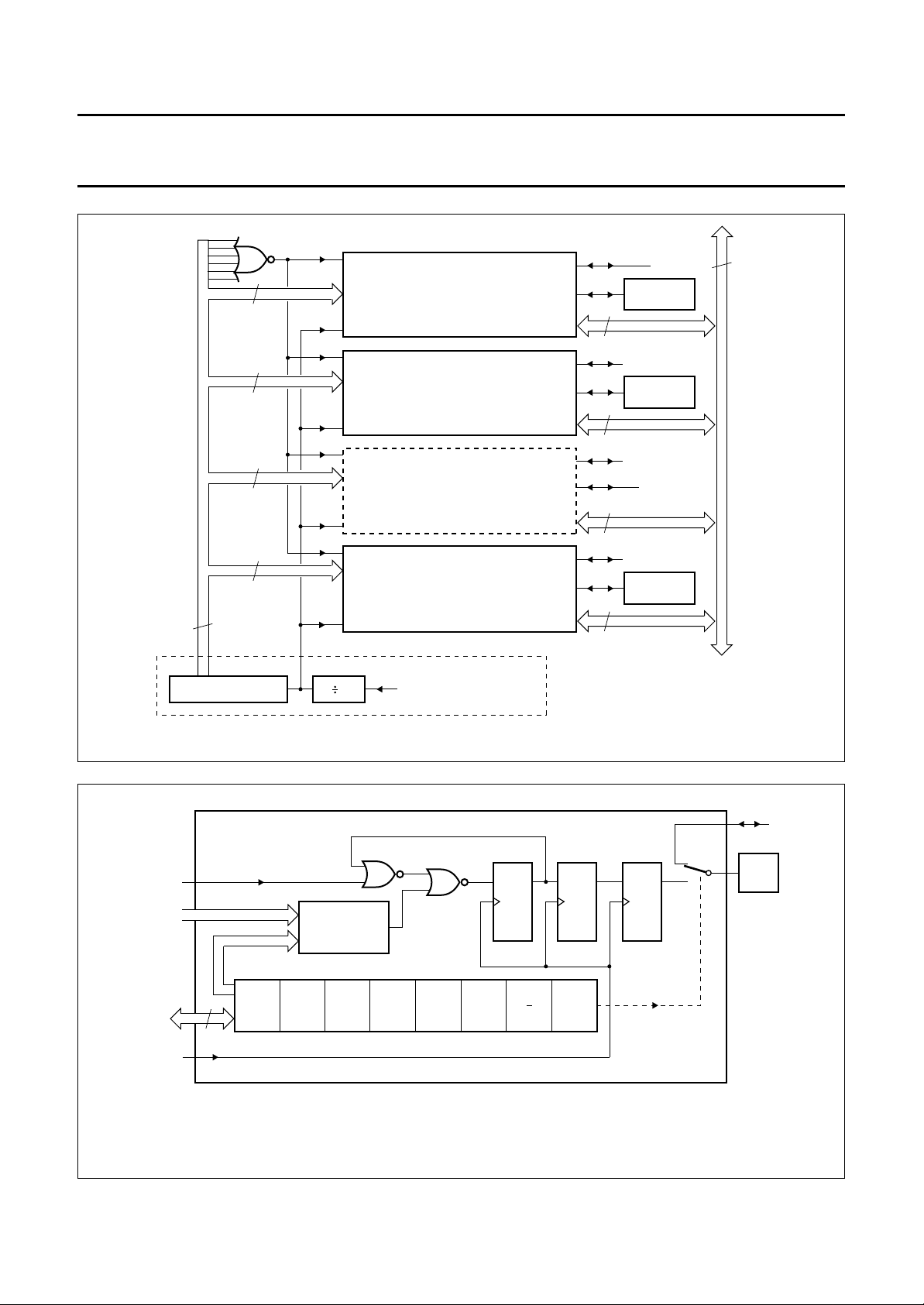
10 6-BIT PWM DACS
Figure 3 shows the 6-bit PWM DAC logic circuit, consisting
of 8 PWMn modules.
The basic MCU clock is divided by 4 to get a waveform that
clocks a 14-bit counter which is common to all the PWMs
(including the 14-bit PWM). This divided clock is hereafter
called the PWM clock.
As illustrated in Fig.3, the lower-precision (6-bit) PWMs
use the least significant part of the 14-bit counter.
Figure 4 shows the circuit diagram of a 6-bit PWM module.
Each PWM module has a Special Function Register
PWMn; n = 0 to 7. The register format is shown in Table 6.
10.1 PWM DAC operation
Value field PVn5 to PVn0 of each PWMn register
(n = 0 to 7) is compared to the 6 LSBs of the common
counter (14-bit counter).
83C145; 83C845
83C055; 87C055
When the value matches, the output flip-flop is cleared, so
that the output pin is driven LOW.
When the value rolls over to zero, the output flip-flop is set,
so that the output pin is released. Thus the output
waveform has a fixed period of 64 PWM clock cycles; its
duty cycle is determined by contents of PWMn.5 to
PWMn.0 (PVn5 to PVn0).
Three of the nine total PWM modules (8 PWMn and the
14-bit PWM DAC) operate as previously described; for
three others, both the rising and falling edges of the output
are delayed by one PWM clock; for the remaining three,
both edges are delayed by two PWM clocks. This feature
reduces the radio-frequency emission that would
otherwise occur when the counter rolled over to zero and
all nine open-drain outputs were released.
10.2 Special Function Register PWMn (n = 0 to 7)
Table 6 Special Function Register PWMn (n = 0 to 7; addresses D4H to DFH)
7 6 5 4 3 2 1 0
PWnE − PVn5 PVn4 PVn3 PVn2 PVn1 PVn0
Table 7 Description of PWMn bits
BIT SYMBOL DESCRIPTION
7 PWnE PWM module enable bit. If for a particular PWM block (n) the bit:
PWnE = 1, then the block is active and controls its assigned port pin.
PWnE = 0, the corresponding port pin is controlled by the port.
6 − Reserved.
5 to 0 PVn5 to PVn0 Value field for PWMn register.
1996 Mar 22 9
Philips Semiconductors Product specification
Microcontrollers for TV and video (MTV)
handbook, full pagewidth
ZERO
6
1st PWM MODULE (n = 0)
6
2nd PWM MODULE (n = 1)
6
3rd to 7th PWM MODULE (n = 2 to 6)
6
8th PWM MODULE (n = 7)
6
8
8
8
8
83C145; 83C845
83C055; 87C055
P1.3
PWM0/P1.3
P0.1
PWM1/P0.1
P0.2 to P0.6
PWM2/P0.2
to
PWM6/P0.6
P0.7
PWM7/P0.7
8
LS 6-bits PWM clock
14-BIT COUNTER
handbook, full pagewidth
(1) This flip-flop occurs in 5 of the 8 PWMn modules.
(2) This flip-flop occurs in 3 of the 8 PWMn modules.
PWM module (n)
ZERO
LS 6-bits
6-bits (PVn0 to PVn5)
8
PVn0 PVn1 PVn2 PVn3 PVn4 PVn5 PWnE
internal bus
PWM clock
4
6-bit
COMPARATOR
f
xtal
14-BIT PWM
DAC BLOCK
Fig.3 6-bit PWM DAC logic circuit.
MBE771 - 1
(1) (2)
internal bus
I/O port
MBE770
PWMn
I/O pin
Fig.4 A 6-bit PWM module.
1996 Mar 22 10

Philips Semiconductors Product specification
Microcontrollers for TV and video (MTV)
11 14-BIT PWM DAC (TDAC)
11.1 14-bit counter
The 14-bit counter was already mentioned in Section 10.
The nature of the counter is such that it can achieve a
stable output value through its MSB, and the value can
propagate through logic like that shown in Fig.5. The logic
output can be stable within:
• one period of the PWM clock (e.g. 250 ns) if
edge-triggered logic is used to capture the logic output,
or
• one phase of the PWM clock (e.g. 125 ns) if a phase of
the PWM clock is used to capture the logic output.
The 14-bit (TDAC) counter is a ripple counter (cost and
die-size reasons).
The 14-bit PWM DAC is controlled by two special function
registers TDACL and TDACH.
11.2 14-bit DAC operation
When software wishes to change the 14-bit value
(TD0 to TD13), it should first write to TDACL and then
write to TDACH. Alternatively, if the required precision of
the duty cycle is satisfied by 6 bits or less, software can
simply write to TDACH (TD8 to TD13).
11.2.1 L
Figure 5 shows that this block includes an ‘extra’ 14-bit
latch between TDACL - TDACH and the comparator and
other logic. The programmed value is clocked into the
operative latch when the 7 low-order bits of the counter roll
over to zero, provided that the software is not in the midst
of loading a new 14-bit value, i.e. it is not between writing
TDACL and writing TDACH.
In a similar fashion to the lower-precision PWMs, this
facility has an output flip-flop that is set when the lower
7 bits of the counter overflow/wrap. The more significant
7 bits of the operative latch’s programmed value are
compared for equality against the less significant 7 bits of
the counter, and the output FF is cleared when they match.
Thus this output has a fixed period of 128 PWM clock
cycles, and the duty cycle is determined by the
programmed value.
OW PRECISION OPERATION
83C145; 83C845
83C055; 87C055
11.2.2 H
For the higher-precision aspect of this feature, the 7 MSBs
of the counter are used in a logic block with the 7 LSBs of
the programmed value.
The 7th LSB (binary value 64) of the programmed value is
ANDed with the 7th MSB (128) of the counter, the 6th LSB
of the value is ANDed with the counter’s 6th and 7th MSBs
being 10, and so on through the LSB of the programmed
value being ANDed with the counter’s 7 MSBs being
100000. Then these 7 ANDed terms are ORed. If the
result is true (logic 1) at the time the 7 LSBs of the counter
match the MSBs of the programmed value, the output is
forced high for 1 (additional) PWM clock cycle.
The result is that, if the value-64 bit of the 14-bit value is
programmed to a logic 1, every other cycle of 128 PWM
counter clocks has its duty cycle stretched by one counter
clock; if the value-32 bit is programmed to logic 1, every
th
cycle is stretched, and so on through, if the value-1 bit
4
is programmed to logic 1, one cycle out of each 128 is
stretched.
11.2.3 14Assuming the external integrator can handle all this, the
net effect is a PWM DAC that has the period of a 7-bit
design (which makes the integrator easier and more
feasible to design) with the accuracy of a 14-bit one.
An obvious prerequisite for such precision is that the load
on the voltage must be very light, like a single op-amp or
comparator.
11.2.3.1 Note
The TDAC feature differs from the corresponding features
of predecessor parts in several ways:
1. The 14-bit value is functionally composed of major and
2. The 14-bit value is programmed as a contiguous
3. As discussed for the 6-bit DACs, both of the preceding
IGH PRECISION OPERATION
BIT DAC OUTPUT
minor portions of 7 bits each.
multi-register value that can be manipulated
straight-forwardly via arithmetic instructions.
parts had a feature whereby the PWM output could be
inverted, redundantly with complementing the 14-bit
value. This feature has been eliminated.
1996 Mar 22 11

Philips Semiconductors Product specification
Microcontrollers for TV and video (MTV)
83C145; 83C845
83C055; 87C055
11.3 Special Function Register TDACL
Table 8 Special Function Register TDACL format (address D2H)
76543210
TD7 TD0 TD1 TD2 TD3 TD4 TD5 TD6
Table 9 Description of TDACL bits
BIT SYMBOL DESCRIPTION
7 to 0 TD7, TD0 to TD6 8 LSBs of the 14-bit value.
11.4 Special Function Register TDACH
Table 10 Special Function Register TDACH format (address D3H)
76543210
TDE − TD13 TD12 TD11 TD10 TD9 TD8
Table 11 Description of TDACH bits
BIT SYMBOL DESCRIPTION
7 TDE Enable bit.
6 − Reserved.
5 to 0 TD13to TD8 6 MSBs of the 14-bit value.
1996 Mar 22 12
 Loading...