

Philips P83CL781HDH, P83CL782HDH, P83CL781HFH, P83CL782HDP, P83CL781HFP Datasheet

INTEGRATED CIRCUITS
DATA SH EET
P83CL781; P83CL782
Low voltage 8-bit microcontrollers
with UART and I
Product specification
Supersedes data of 1995 Jul 13
File under Integrated Circuits, IC20
2
C-bus
1997 Mar 14

Philips Semiconductors Product specification
Low voltage 8-bit microcontrollers with
UART and I
CONTENTS
1 FEATURES
2 GENERAL DESCRIPTION
3 APPLICATIONS
4 ORDERING INFORMATION
5 BLOCK DIAGRAM
6 FUNCTIONAL DIAGRAM
7 PINNING INFORMATION
7.1 Pinning
7.2 Pin description
8 FUNCTIONAL DESCRIPTION OVERVIEW
8.1 General
8.2 CPU timing
9 MEMORY ORGANIZATION
9.1 Program memory
9.2 Data memory
9.3 Special Function Registers
9.4 Addressing
10 I/O FACILITIES
10.1 Ports
10.2 Port options
10.3 Port 0 options
10.4 SET/RESET options
11 TIMER/EVENT COUNTERS
11.1 Timer 0 and Timer 1
11.2 Timer T2
11.3 Timer/Counter 2 Control Register (T2CON)
12 REDUCED POWER MODES
12.1 Idle mode
12.2 Power-down mode
12.3 Wake-up from Power-down mode
12.4 Status of external pins
12.5 Power Control Register (PCON)
13 I2C-BUS SERIAL I/O
13.1 Serial Control Register (S1CON)
13.2 Serial Status Register (S1STA)
13.3 Data Shift Register (S1DAT)
13.4 Address Register (S1ADR)
2
C-bus
P83CL781; P83CL782
14 STANDARD SERIAL INTERFACE SIO0: UART
14.1 Multiprocessor communications
14.2 Serial Port Control and Status Register
(S0CON)
14.3 Baud rates
15 INTERRUPT SYSTEM
15.1 External interrupts INT2 to INT9
15.2 Interrupt priority
15.3 Interrupt registers
16 OSCILLATOR CIRCUITRY
17 RESET
17.1 External reset using the RST pin
17.2 Power-on reset
18 SPECIAL FUNCTION REGISTERS
OVERVIEW
19 INSTRUCTION SET
20 LIMITING VALUES
21 DC CHARACTERISTICS
22 AC CHARACTERISTICS
22.1 Program memory
22.2 External Data Memory
23 PACKAGE OUTLINES
24 SOLDERING
24.1 Introduction
24.2 DIP
24.3 QFP
25 DEFINITIONS
26 LIFE SUPPORT APPLICATIONS
27 PURCHASE OF PHILIPS I2C COMPONENTS
1997 Mar 14 2

Philips Semiconductors Product specification
Low voltage 8-bit microcontrollers with
UART and I
1 FEATURES
• Full static 80C51 CPU
• 8-bit CPU, ROM, RAM, I/O in a 40-lead DIP or 44-lead
QFP package
• 16 kbytes ROM, expandable externally to 64 kbytes
• 256 bytes RAM, expandable externally to 64 kbytes
• Four 8-bit ports, 32 I/O lines
• Three 16-bit timer/event counters
• External memory expandable up to 128 kbytes: RAM up
to 64 kbytes and ROM up to 64 kbytes
• On-chip oscillator suitable for RC, LC, quartz crystal or
ceramic resonator
• Fifteen source, fifteen vector interrupt structure with two
priority levels
• Full duplex serial port (UART)
2
C-bus interface for serial transfer on two lines
• I
• Enhanced architecture with:
– non-page oriented instructions
– direct addressing
– four 8 byte RAM register banks
– stack depth limited only by available internal RAM
(maximum 256 bytes)
– multiply, divide, subtract and compare instructions
• Reduced power consumption through Power-down and
Idle modes
• Wake-up via external interrupts at Port 1
• Single supply voltage of 1.8 to 6.0 V
• Operating ambient temperature:
– 83CL781: −40 to +85 °C
– 83CL782: −25 to +55 °C.
• Frequency range of DC to 12 MHz
• Very low current consumption.
2
C-bus
P83CL781; P83CL782
2 GENERAL DESCRIPTION
The term P83CL78x is used throughout this data sheet to
refer to both the P83CL781 and P83CL782; differences
between the devices are highlighted in the text.
The P83CL78x is manufactured in an advanced CMOS
technology. The P83CL78x has the same instruction set
as the 80C51, consisting of over 100 instructions:
49 one-byte, 46 two-byte, and 16 three-byte. The device
has low power consumption and a wide range of supply
voltage; there are two software-selectable modes of
reduced activity for further power reduction: Idle and
Power-down. For emulation purposes, the P85CL781
(piggy-back version) with 256 bytes of RAM is
recommended.
The P83CL782 is a faster version of the P83CL781 and
operates at a maximum frequency of 12 MHz at
VDD≥ 3.1 V.
This data sheet details the specific properties of the
P83CL78x. For details of the 80C51 core and the I2C-bus
see
“Data Handbook IC20”
3 APPLICATIONS
The P83CL78x is an 8-bit general purpose microcontroller
especially suited for cordless telephone applications.
The P83CL78x also functions as an arithmetic processor
having facilities for both binary and BCD arithmetic plus
bit-handling capabilities.
.
1997 Mar 14 3
Philips Semiconductors Product specification
Low voltage 8-bit microcontrollers with
UART and I
4 ORDERING INFORMATION
TYPE NUMBER
P83CL781HFP DIP40 plastic dual in-line package; 40 leads (600 mil) SOT129-1
P83CL782HDP
P83CL781HFH QFP44 plastic quad flat package; 44 leads (lead length 2.35 mm);
P83CL782HDH
P83CL781HFH QFP44 plastic quad flat package; 44 leads (lead length 1.3 mm);
P83CL781HDH
Note
1. Refer to the Order Entry Form (OEF) for this device for the full type number, including options/program.
2
C-bus
(1)
PACKAGE
NAME DESCRIPTION VERSION
body 14 × 14 ×2.2 mm
body 10 × 10 × 1.75 mm
P83CL781; P83CL782
SOT205-1
SOT307-2
1997 Mar 14 4
Philips Semiconductors Product specification
Low voltage 8-bit microcontrollers with
UART and I
5 BLOCK DIAGRAM
handbook, full pagewidth
2
C-bus
XTAL1
XTAL2
EA
ALE
PSEN
WR
RD
RST
T0 T1 INT0 INT1
3 3 3 3
TWO
16-BIT
TIMER/
EVENT
COUNTERS
(T0, T1)
80C51
core
excluding
ROM/RAM
3
3
CPU
PROGRAM
MEMORY
16 kbyte
ROM
P83CL781; P83CL782
DATA
MEMORY
256 byte
RAM
8-bit internal bus
P83CL781
P83CL782
MLA601
V
DD
AD0 to 7
A8 to 15
0
2
0
alternative function of Port 0
1
alternative functions of Port 1
PARALLEL
I/O PORTS
AND
EXTERNAL
BUS
SERIAL
UART
PORT
33 1
RXDTXDP3P2P1P0
2
alternative function of Port 2
3
alternative function of Port 3
16-BIT
TIMER/
EVENT
COUNTER
1
T2
Fig.1 Block diagram.
INTERFACE
1 1
T2EX
2
C
I
V
SS
SDASCL
1997 Mar 14 5
Philips Semiconductors Product specification
Low voltage 8-bit microcontrollers with
UART and I
6 FUNCTIONAL DIAGRAM
handbook, full pagewidth
2
C-bus
XTAL1
XTAL2
EA
PSEN
ALE
PORT 0
PORT 1
P83CL781; P83CL782
LOW ORDER
ADDRESS
AND
DATA BUS
(AD0 to AD7)
T2 INT2
T2EX INT3
INT4
SCL
SDA
INT5
INT6
INT7
INT8
INT9
RST
P83CL781
P83CL782
PORT 2
PORT 3
V
SS
V
DD
MBH885
Fig.2 Functional diagram.
HIGH ORDER
ADDRESS
BUS
(A8 to A15)
RXD/data
TXD/clock
INT0
INT1
T0
T1
WR
RD
1997 Mar 14 6
Philips Semiconductors Product specification
Low voltage 8-bit microcontrollers with
UART and I
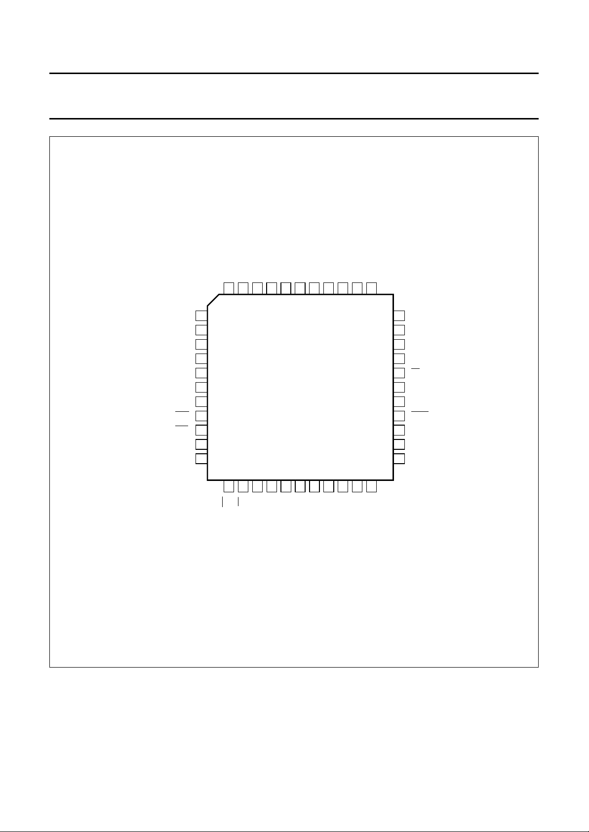
7 PINNING INFORMATION
7.1 Pinning
2
C-bus
P1.0/INT2/T2
P1.1/INT3/T2EX
P1.2/INT4
P1.3/INT5
P1.4/INT6
P1.5/INT7
P1.6/INT8/SCL
P1.7/INT9/SDA
RST
P3.0/RXD/data
P3.1/TXD/clock
P3.2/INT0
1
2
3
4
5
6
7
8
9
10
11
12
P83CL781
P83CL782
40
39
38
37
36
35
34
33
32
31
30
29
V
DD
P0.0/AD0
P0.1/AD1
P0.2/AD2
P0.3/AD3
P0.4/AD4
P0.5/AD5
P0.6/AD6
P0.7/AD7
EA
ALE
PSEN
P83CL781; P83CL782
P3.3/INT1
P3.4/T0
P3.5/T1
P3.6/WR
P3.7/RD
XTAL2
XTAL1
V
SS
13
14
15
16
17
18
19
20
MLA603
28
27
26
25
24
23
22
21
P2.7/A15
P2.6/A14
P2.5/A13
P2.4/A12
P2.3/A11
P2.2/A10
P2.1/A9
P2.0/A8
Fig.3 Pin configuration for DIP40 package.
1997 Mar 14 7
Philips Semiconductors Product specification
Low voltage 8-bit microcontrollers with
UART and I
handbook, full pagewidth
2
C-bus
P1.5/INT7
P1.6/INT8/SCL
P1.7/INT9/SDA
P3.0/RXD/data
P3.1/TXD/clock
P3.2/INT0
P3.3/INT1
RST
n.c.
P3.4/T0
P3.5/T1
P1.2/INT4
P1.3/INT5
P1.4/INT6
44
43
42
1
2
3
4
5
6
7
8
9
10
11
n.c.
P1.0/INT2/T2
P1.1/INT3/T2EX
41
V
40
39
P83CL781
P83CL782
DD
38
P0.1/AD1
P0.0/AD0
37
36
P83CL781; P83CL782
P0.3/AD3
P0.2/AD2
35
34
33
P0.4/AD4
32
P0.5/AD5
31
P0.6/AD6
30
P0.7/AD7
29
EA
28
n.c.
27
ALE
26
PSEN
25
P2.7/A15
24
P2.6/A14
23
P2.5/A13
20
21
P2.2/A10
P2.3/A11
22
P2.4/A12
12
13
P3.7/RD
P3.6/WR
14
XTAL2
15
V
XTAL1
16
SS
17
18
SS
TEST/V
19
P2.0/A8
P2.1/A9
Fig.4 Pin configuration for QFP44 packages.
MLA604
1997 Mar 14 8
Philips Semiconductors Product specification
Low voltage 8-bit microcontrollers with
UART and I
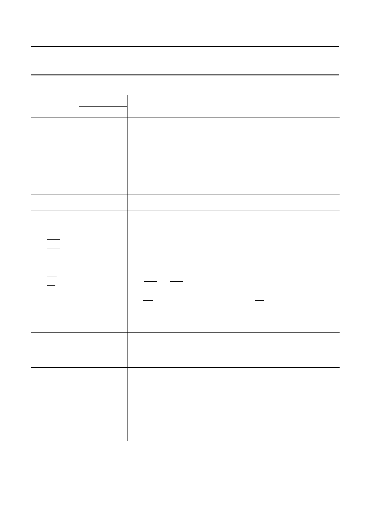
7.2 Pin description
SYMBOL
P1.0/INT2/T2 1 40 • Port 1: 8-bit bidirectional I/O port (P1.0 to P1.7). Port pins that have logic 1s
P1.1/INT3/T2EX 2 41
P1.2/INT4 3 42
P1.3/INT5 4 43
P1.4/INT6 5 44
P1.5/INT7 6 1
P1.6/INT8/SCL 7 2
P1.7/INT9/SDA 8 3
RST 9 4 Reset: A HIGH level on this pin for two machine cycles while the oscillator is
n.c. − 6 Not connected.
P3.0/RXD/data 10 5 • Port 3: 8-bit bidirectional I/O port (P3.0 to P3.7).
P3.1/TXD/clock 1 1 7
P3.2/INT0 12 8
INT1 13 9
P3.3/
P3.4/T0 14 10
P3.5/T1 15 11
WR 16 12
P3.6/
RD 17 13
P3.7/
XT AL2 18 14 Crystal Output: Output of the inverting amplifier that forms the oscillator. Left
XTAL1 19 15 Crystal Input: Input to the inverting amplifier that forms the oscillator, also the
V
SS
TEST/V
P2.0/A8 21 18 • Port 2: 8-bit bidirectional I/O port (P2.0 to P2.7).
P2.1/A9 22 19
P2.2/A10 23 20
P2.3/A1 1 24 21
P2.4/A12 25 22
P2.5/A13 26 23
P2.6/A14 27 24
P2.7/A15 28 25
SS
2
C-bus
PIN
DIP40 QFP44
written to them are pulled HIGH by internal pull-ups, and in this state can be
used as inputs (note that P1.6 and P1.7 are open-drain only). As inputs, Port 1
pins that are externally pulled LOW will source current (I
pull-ups. Port 1 output buffers can sink/source 4 LS TTL loads.
• Alternative functions:
– INT2 to INT9 are external interrupt inputs
– T2 and T2EX are the Timer/event counter 2 inputs
– SCL and SDA are the I
running, resets the device.
Same characteristics as Port 1.
• Alternative functions:
– RXD/data is the UART serial data input (asynchronous) or data I/O
(synchronous)
– TXD/clock is the UART serial data output (asynchronous) or clock output
(synchronous)
INT0 and INT1 are external interrupt lines
–
– T0 and T1 are external inputs for Timer 0 and Timer 1 respectively
– WR is the external memory write strobe andRD is the external memory read
strobe.
open-circuit when an external oscillator clock is used.
input for an externally generated clock source.
20 16 Ground: Circuit ground potential.
− 17 Test Input: Must be connected to VSS or left open.
Same characteristics as Port 1.
• High-order addressing: A8 to A15 make up the high-order address byte
during accesses to external memory that use 16-bit addresses
(MOVX@DPTR). In this application the pins use the strong internal pull-ups
when emitting logic 1's. During accesses to external memory that use 8-bit
addresses (MOVX@Ri), the pins emit the contents of the P2 Special Function
Register.
DESCRIPTION
2
C-bus clock and data lines.
P83CL781; P83CL782
) due to the internal
IL
1997 Mar 14 9

Philips Semiconductors Product specification
Low voltage 8-bit microcontrollers with
UART and I
SYMBOL
PSEN 29 26 Program Store Enable: Read strobe to external Program Memory. When
ALE 30 27 Address Latch Enable: Latches the low byte of the address during accesses to
n.c. − 28 Not connected.
EA 31 29 External Access: When EA is held HIGH, the CPU executes out of the internal
P0.7/AD7 32 30 • Port 0: 8-bit open-drain bidirectional I/O port (P0.7 to P0.0). As an open-drain
P0.6/AD6 33 31
P0.5/AD5 34 32
P0.4/AD4 35 33
P0.3/AD3 36 34
P0.2/AD2 37 35
P0.1/AD1 38 36
P0.0/AD0 39 37
V
DD
n.c. − 39 Not connected.
2
C-bus
PIN
DIP40 QFP44
executing code out of external Program Memory, PSEN is activated twice each
machine cycle. However, during each access to external Data Memory two
PSEN activations are skipped.
external memory . It is activated every six oscillator periods and may be used for
external timing or clocking purposes.
Program Memory (unless the Program Counter exceeds 3FFFH). When EA is
held LOW, the CPU executes out of external Program Memory regardless of the
value of the program counter.
output port it can sink/source 8 LS TTL loads. Port 0 pins that have logic 1s
written to them float, and in this state will function as high-impedance inputs.
• Low-order addressing: AD7 to AD0 provide the multiplexed low-order
address and data bus during accesses to external memory . In this application
the pins use the strong internal pull-ups when emitting logic 1s.
40 38 Power supply.
DESCRIPTION
P83CL781; P83CL782
1997 Mar 14 10

Philips Semiconductors Product specification
Low voltage 8-bit microcontrollers with
UART and I
8 FUNCTIONAL DESCRIPTION OVERVIEW
This chapter gives a brief overview of the device. The
detailed functional description is in the following chapters:
Chapter 9 “Memory organization”
Chapter 10 “I/O facilities”
Chapter 11 “Timer/event counters”
Chapter 12 “Reduced power modes”
Chapter 13 “I2C-bus serial I/O”
Chapter 14 “Standard serial interface SIO0: UART”
Chapter 15 “Interrupt system”
Chapter 16 “Oscillator circuitry”
Chapter 17 “Reset”.
8.1 General
The P83CL78x is a stand-alone high-performance CMOS
microcontroller designed for use in real-time applications
such as instrumentation, industrial control, intelligent
computer peripherals and consumer products. The device
provides hardware features, architectural enhancements
and new instructions to function as a controller for
applications requiring up to 64 kbytes of Program Memory
and/or up to 64 kbytes of data storage.
2
C-bus
P83CL781; P83CL782
The device has two software-selectable modes of reduced
activity for power reduction:
• Idle mode; freezes the CPU while allowing the timers,
serial I/O and interrupt system to continue functioning.
• Power-down mode; saves the RAM contents but
freezes the oscillator causing all other chip functions to
be inoperative.
In addition, two serial interfaces are provided on-chip:
• a standard UART serial interface, and
2
• a standard I
interface has byte-oriented master and slave functions
allowing communication with the whole family of I2C-bus
compatible devices.
8.2 CPU timing
A machine cycle consists of a sequence of 6 states. Each
state lasts for two oscillator periods, thus a machine cycle
takes 12 oscillator periods or 1 µs if the oscillator
frequency (f
C-bus serial interface. The I2C-bus serial
) is 12 MHz.
osc
The P83CL78x contains a non-volatile 16 kbyte read-only
Program Memory; a static 256 byte read/write Data
Memory; 32 I/O lines; three 16-bit timer/event counters; a
fifteen-source, two priority-level, nested interrupt structure
and on-chip oscillator and timing circuit.
1997 Mar 14 11

Philips Semiconductors Product specification
Low voltage 8-bit microcontrollers with
UART and I
9 MEMORY ORGANIZATION
The P83CL78x has a 16 kbyte Program Memory (ROM)
plus 256 bytes of Data Memory (RAM) on-chip. The device
has separate address spaces for Program and Data
Memory (see Fig.6). Using Ports P0 and P2, the
P83CL78x can address up to 128 kbytes of external
memory. The CPU generates both read (RD) and write
(WR) signals for external Data Memory accesses, and the
read strobe (PSEN) for external Program Memory.
9.1 Program memory
The P83CL78x contains 16 kbytes of internal ROM. After
reset the CPU begins execution at location 0000H.
The lower 16 kbytes of Program Memory can be
implemented in either on-chip ROM or external memory.
If the
EA pin is strapped to VDD, then Program Memory
fetches from addresses 0000H through to 3FFFH are
directed to the internal ROM. Fetches from addresses
4000H through to FFFFH are directed to external ROM.
Program Counter values greater than 3FFFH are
automatically addressed to external memory regardless of
the state of the EA pin.
2
C-bus
P83CL781; P83CL782
9.4 Addressing
The P83CL78x has five methods for addressing source
operands:
• Register
• Direct
• Register-indirect
• Immediate
• Base-register plus index-register-indirect.
The first three methods can be used for addressing
destination operands. Most instructions have a
‘destination/source’ field that specifies the data type,
addressing methods and operands involved.
For operations other than MOVs, the destination operand
is also a source operand.
lfpage
7FH
9.2 Data memory
The P83CL78x contains 256 bytes of internal RAM and
34 Special Function Registers (SFRs). The memory map
(Fig.6 ) shows the internal Data Memory space divided into
the lower 128 bytes, the upper 128 bytes and the SFR
space. Internal RAM locations 0 to 127 are directly and
indirectly addressable. Internal RAM locations 128 to 255
are only indirectly addressable. The Special Function
Register locations 128 to 255 bytes are only directly
addressable.
9.3 Special Function Registers
The upper 128 bytes are the address locations of the
Special Function Registers. Figures 7 and 8 show the
Special Function Registers space. The SFRs include the
port latches, timers, peripheral control, serial I/O registers,
and so on. These registers can only be accessed by direct
addressing. There are 128 addressable locations in the
SFR address space (SFRs with addresses divisible by
eight).
30H
2FH
bit-addressable space
(bit addresses 0 to 7F)
20H
R7
R0
R7
R0
R7
R0
R7
R0
1FH
18H
17H
10H
0FH
08H
07H
4 banks of 8 registers
0
MLA560 - 1
(R0 to R7)
Fig.5 The lower 128 bytes of internal RAM.
1997 Mar 14 12
Philips Semiconductors Product specification
Low voltage 8-bit microcontrollers with
UART and I
Access to memory addressing is as follows:
• Registers in one of the four register banks through
register, direct or register-indirect
• 256 bytes of internal data RAM through direct or
register-indirect
• Special Function Registers through direct
• External Data Memory through register-indirect
• Program Memory look-up tables through base-register
plus index-register-indirect.
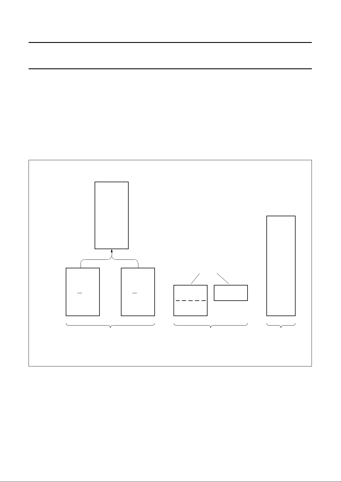
handbook, full pagewidth
2
C-bus
64 kbytes
EXTERNAL
P83CL781; P83CL782
The P83CL78x is classified as an 8-bit device since the
internal ROM, RAM, Special Function Registers,
Arithmetic Logic Unit and external data bus are all 8-bits
wide. It performs operations on bit, nibble, byte and
double-byte data types.
Facilities are available for byte transfer, logic and integer
arithmetic operations. Data transfer, logic and conditional
branch operations can be performed directly on Boolean
variables to provide excellent bit handling.
64 kbytes
16 kbytes
16 kbytes
INTERNAL
(EA = 1)
16 kbytes
PROGRAM MEMORY
EXTERNAL
(EA = 0)
OVERLAPPED SPACE
255
(INDIRECT
127
ONLY)
INTERNAL
DATA RAM
0
INTERNAL DATA MEMORY
Fig.6 Memory map.
SPECIAL
FUNCTION
REGISTERS
MLA605
0
EXTERNAL
DATA MEMORY
1997 Mar 14 13
Philips Semiconductors Product specification
Low voltage 8-bit microcontrollers with
UART and I
2
C-bus
REGISTER
MNEMONIC
IP1
B
IX1
IEN1
BIT ADDRESS
FEFF FD FC FB FA F9 F8
F6F7 F5 F4 F3 F2 F1 F0
EEEF ED EC EB EA E9 E8
DIRECT
BYTE
ADDRESS (HEX)
FFH
FEH
FDH
FCH
F8H
F0H
EFH
EEH
EDH
ECH
EBH
EAH
E9H
E8H
P83CL781; P83CL782
ACC
S1ADR
S1DAT
S1STA
S1CON
PSW
TH2
TL2
RCAP2H
RCAP2L
T2CON
IRQ1
E6E7 E5 E4 E3 E2 E1 E0
DEDF DD DC DB DA D9 D8
D6D7 D5 D4 D3 D2 D1 D0
CECF CD CC CB CA C9 C8
C6C7 C5 C4 C3 C2 C1 C0
E0H
DBH
DAH
D9H
D8H
D0H
CFH
CEH
CDH
CCH
CBH
CAH
C9H
C8H
C0H
MLA606 - 1
SFRs containing
directly addressable
bits
Fig.7 Special Function Register memory map (continued in Fig.8).
1997 Mar 14 14

Philips Semiconductors Product specification
Low voltage 8-bit microcontrollers with
UART and I
2
C-bus
REGISTER
MNEMONIC
IP0
P3
IEN0
BIT ADDRESS
BE BD BC BB BA B9 B8
B6B7 B5 B4 B3 B2 B1 B0
AEAF AD AC AB AA A9 A8
DIRECT
BYTE
ADDRESS (HEX)
B8H
B0H
AFH
AEH
ADH
ACH
ABH
AAH
A9H
A8H
P83CL781; P83CL782
P2
S0BUF
S0CON
P1
TH1
TH0
TL1
TL0
TMOD
TCON
PCON
DPH
DPL
SP
P0
A6A7 A5 A4 A3 A2 A1 A0
9E9F 9D 9C 9B 9A 99 98
9697 95 94 93 92 91 90
8E8F 8D 8C 8B 8A 89 88
8687 85 84 83 82 81 80
A0H
99H
98H
90H
8DH
8CH
8BH
8AH
89H
88H
87H
83H
82H
81H
80H
SFRs containing
directly addressable
bits
MLA607
Fig.8 Special Function Register memory map (continued from Fig.7).
1997 Mar 14 15

Philips Semiconductors Product specification
Low voltage 8-bit microcontrollers with
UART and I
10 I/O FACILITIES
10.1 Ports
The P83CL78x has 32 I/O lines treated as 32 individually
addressable bits or as four parallel 8-bit ports. To enable a
port pin alternative function, the port bit latch in its SFR
must contain a logic 1. The alternative functions are
detailed below:
Port 0 Provides the multiplexed low-order address and
data bus for expanding the device with standard
memories and peripherals.
Port 1 Used for a number of special functions:
• Provides the inputs for the eight external
interrupts: INT2 to INT9
• External activation of Timer 2: T2
• The I
Port 2 Provides the high-order address when expanding
the device with external Program or Data memory.
Port 3 Pins can be configured individually to provide:
• External interrupt request inputs: INT1 and INT0
• Timer/counter inputs: T1 and T0
• Control signals to read and write to external
memories: RD and WR
• UART asynchronous input and output (RXD and
TXD); or UART synchronous I/O and clock lines
(data and clock).1
Each port consists of a latch (SFRs P0 to P3), an output
driver and input buffer. Ports 1, 2 and 3 have internal
pull-ups (except P1.6 and P1.7). Figure 9(a) shows that
the strong transistor ‘p1’ is turned on for only 2 oscillator
periods after a LOW-to-HIGH transition in the port latch.
When on, it turns on p3 (a weak pull-up) through the
inverter. This inverter and p3 form a latch which holds the
logic 1. In Port 0 the pull-up ‘p1’ is only on when emitting
logic 1s for external memory access. Writing a logic 1 to a
Port 1 bit latch leaves both output transistors switched off
so that the pin can be used as an high-impedance input.
2
C-bus
2
C-bus interface: SCL and SDA.
P83CL781; P83CL782
LOW-to-HIGH transition in the port latch;
Fig.9(a).
Option 2 Open-drain; quasi-bidirectional I/O with
n-channel open-drain output. Use as an output
requires the connection of an external pull-up
resistor; Fig.9(b).
Option 3 Push-Pull; output with drive capability in both
polarities. Under this option, pins can only be
used as outputs; Fig.9(c).
10.3 Port 0 options
The definition of port options for Port 0 is slightly different.
Two cases are considered. First, access to external
memory (
boundary) and second, I/O accesses.
10.3.1 E
Option 1 True logic 0 and logic 1 are written as address to
Option 2 An external pull-up resistor is required for
Option 3 Not allowed for external memory accesses as
10.3.2 I/O A
Option 1 When writing a logic 1 to the port latch, the
Option 2 Open-drain; quasi-directional I/O with n-channel
Option 3 Push-Pull; output with drive capability in both
EA = 0 or access above the built-in memory
XTERNAL MEMORY ACCESSES
the external memory (strong pull-up to be used).
external accesses.
the port can only be used as output.
CCESSES
strong pull-up ‘p1’ will be on for 2 oscillator
periods. No weak pull-up exists. Without an
external pull-up, this option can be used as a
high-impedance input.
open-drain output. Use as an output requires the
connection of an external pull-up resistor. See
Fig.9(b).
polarities. Under this option pins can only be
used as outputs. See Fig.9(c).
10.2 Port options
30 of the 32 port pins (excluding P1.6 and P1.7 with option
2S only) may be individually configured with one of the
following options. These options are also shown in Fig.9.
Option 1 Standard Port; quasi-bidirectional I/O with
pull-up. The strong booster pull-up ‘p1’ is turned
on for two oscillator periods after a
1997 Mar 14 16
10.4 SET/RESET options
Individual mask selection of the post-reset state is
available with any of the above pins. The required
selection is made by appending ‘S’ or ‘R’ to Options 1, 2,
or 3 above.
Option R RESET, at reset this pin will be initialized LOW.
Option S SET, at reset this pin will be initialized HIGH.

Philips Semiconductors Product specification
Low voltage 8-bit microcontrollers with
UART and I
handbook, full pagewidth
from port latch
2
input data
read port pin
C-bus
Q
2 oscillator
periods
strong pull-up
INPUT
BUFFER
(a) Standard
P83CL781; P83CL782
+5 V
p2
p1
n
p3
I/O pin
+5 V
from port latch
read port pin
from port latch
Q
input data
Q
n
INPUT
BUFFER
(b) Open-drain
strong pull-up
+5 V
external
pull-up
I/O pin
p1
I/O pin
n
(c) Push-pull
Fig.9 Port configuration options.
1997 Mar 14 17
MGD677

Philips Semiconductors Product specification
Low voltage 8-bit microcontrollers with
UART and I
11 TIMER/EVENT COUNTERS
The P83CL78x contains three 16-bit timer/event counter
registers; Timer 0, Timer 1 and Timer 2 which can perform
the following functions:
• Measure time intervals and pulse durations
• Count events
• Generate interrupt requests.
In the ‘Timer’ operating mode the register is incremented
every machine cycle. Since a machine cycle consists of
12 oscillator periods, the count rate is1⁄12× f
In the ‘Counter’ operating mode, the register is
incremented in response to a HIGH-to-LOW transition.
Since it takes 2 machine cycles (24 oscillator periods) to
recognize a HIGH-to-LOW transition, the maximum count
1
rate is
should be held for at least one complete machine cycle.
11.1 Timer 0 and Timer 1
Timer 0 and Timer 1 can be programmed independently to
operate in four modes:
Mode 0 8-bit timer or 8-bit counter each with divide-by-32
Mode 1 16-bit time-interval or event counter.
Mode 2 8-bit time-interval or event counter with automatic
Mode 3 Timer 0 establishes TL0 and TH0 as two
11.2 Timer T2
⁄24× f
prescaler.
reload upon overflow.
separate counters.
2
C-bus
.
osc
. To ensure a given level is sampled, it
osc
P83CL781; P83CL782
11.2.1 C
Figure 10 shows the Capture mode. Two options in this
mode, may be selected by the EXEN2 bit in T2CON:
• If EXEN2 = 0, then Timer 2 is a 16-bit timer or counter
which upon overflowing sets the Timer 2 overflow bit
TF2, this may then be used to generate an interrupt.
• If EXEN2 = 1, Timer 2 operates as described above but
with the additional feature that a HIGH-to-LOW
transition at external input T2EX causes the current
value in TL2 and TH2 to be captured into registers
RCAP2L and RCAP2H respectively. In addition, the
transition at T2EX causes the EXF2 bit in T2CON to be
set; this may also be used to generate an interrupt.
11.2.2 A
Figure 11 shows the Auto-reload mode. Also two options
in this mode are selected by the EXEN2 bit in T2CON:
• If EXEN2 = 0, then when Timer 2 rolls over, it sets the
TF2 bit but also causes the Timer 2 registers to be
reloaded with the 16-bit value held in registers RCAP2L
and RCAP2H. The 16-bit value held in these registers is
preset by software.
• If EXEN2 = 1, Timer 2 operates as described above but
with the additional feature that a HIGH-to-LOW
transition at external input T2EX will also trigger the
16-bit reload and set the EXF2 bit.
11.2.3 B
The Baud Rate Generator mode is selected when
RTCLK = 1. It will be described in conjunction with the
serial port (UART); see Section 14.3.2.
APTURE MODE
UTO-RELOAD MODE
AUD RATE GENERATOR MODE
Timer T2 is a 16-bit timer/counter that can operate (like
Timer 0 and 1) either as a timer or as an event counter.
These functions are selected by the state of the C/
the T2CON register; see Tables 1 and 2.
Three operating modes are available Capture, Auto-reload
and Baud Rate Generator, which also are selected via the
T2CON register; see Table 3.
1997 Mar 14 18
T2 bit in

Philips Semiconductors Product specification
Low voltage 8-bit microcontrollers with
UART and I
handbook, full pagewidth
2
C-bus
12OSC
T2 PIN
T2EX PIN
C/T2 = 0
C/T2 = 1
transition
detector
control
TR2
capture
control
EXEN2
TL2
(8 BITS)
RCAP2L RCAP2H
TH2
(8 BITS)
P83CL781; P83CL782
TF2
Timer 2
interrupt
EXF2
MLA608
handbook, full pagewidth
T2 PIN
T2EX PIN
12OSC
C/T2 = 0
C/T2 = 1
transition
detector
Fig.10 Timer 2 in Capture mode.
TH2
(8 BITS)
control
EXEN2
TR2
reload
control
TL2
(8 BITS)
RCAP2L RCAP2H
TF2
EXF2
MLA609
Timer 2
interrupt
Fig.11 Timer 2 in Auto-Reload mode.
1997 Mar 14 19
Philips Semiconductors Product specification
Low voltage 8-bit microcontrollers with
UART and I
11.3 Timer/Counter 2 Control Register (T2CON)
Table 1 Timer/Counter 2 Control Register (SFR address C8H)
76543210
TF2 EXF2 GF2 RTCLK EXEN2 TR2 C/
Table 2 Description of T2CON bits
BIT SYMBOL DESCRIPTION
7 TF2 Timer 2 overflow flag. Set by a Timer 2 overflow and must be cleared by software. TF2
6 EXF2 Timer 2 external flag. Set when either a capture or reload is caused by a negative
5 GF2 General purpose flag bit.
4 RTCLK Receive/transmit clock flag. When set, causes the UART serial port to use Timer 2
3 EXEN2 Timer 2 external enable flag. When set, allows a capture or reload to occur as a result
2 TR2 Start/stop control for Timer 2. TR2 = 1 starts the timer.
1C/
0 CP/
2
C-bus
will not be set when RTCLK = 1.
transition on T2EX and when EXEN2 = 1. When Timer T2 interrupt is enabled,
EXF2 = 1 will cause the CPU to vector to Timer 2 interrupt routine. EXF2 must be
cleared by software.
overflow pulses for its receive and transmit clock in Modes 1 and 3. RTCLK = 0 causes
Timer 1 overflows to be used for the receive and transmit clock.
of a negative transition on T2EX, if Timer 2 is not being used to clock the serial port.
EXEN2 = 0, causes Timer 2 to ignore events at T2EX.
T2 Timer or counter select for Timer 2. C/T2 = 0 selects the internal timer with a clock
frequency of1⁄12× f
triggered.
RL2 Capture/Reload flag. When set, captures will occur on negative transitions at T2EX, if
EXEN2 = 1. When cleared, auto-reloads will occur either with Timer 2 overflows or
negative transitions at T2EX when EXEN2 = 1. When RTCLK = 1, this bit is ignored and
the timer is forced to auto-reload on a Timer 2 overflow.
. C/T2 = 1 selects the external event counter; negative edge
osc
P83CL781; P83CL782
T2 CP/RL2
Table 3 Timer 2 operating modes; X = don’t care
RTCLK CP/
0 0 1 16-bit Auto-reload
0 1 1 16-bit Capture
1 X 1 Baud Rate Generator
XX0Off
1997 Mar 14 20
RL2 TR2 MODE

Philips Semiconductors Product specification
Low voltage 8-bit microcontrollers with
UART and I
12 REDUCED POWER MODES
There are two software-selectable modes which further
reduce power consumption: ‘Idle’ and ‘Power-down’.
12.1 Idle mode
Operation in Idle mode permits the interrupt, serial ports
and timer blocks to continue to function while the clock to
the CPU is halted.
Idle mode is entered by setting the IDL bit in the Power
Control Register (PCON.0, see Table 5). The instruction
that sets IDL is the last instruction executed in the normal
operating mode before the Idle mode is activated.
Once in the Idle mode, the CPU status is preserved along
with the Stack Pointer, Program Counter, Program Status
Word and Accumulator. The RAM and all other registers
maintain their data during Idle mode. The status of the
external pins during Idle mode is shown in Table 4.
The following functions remain active during the Idle
mode:
• Timer 0, Timer 1 and Timer 2
• UART, I
• External interrupt.
These functions may generate an interrupt or reset; thus
ending the Idle mode.
There are two ways to terminate the Idle mode:
1. Activation of any enabled interrupt will cause PCON.0
2. The second way of terminating the Idle mode is with an
2
C-bus interface
to be cleared by hardware thus terminating the Idle
mode. The interrupt is serviced, and following the
RETI instruction, the next instruction to be executed
will be the one following the instruction that put the
device in the Idle mode. The flag bits GF0 and GF1
may be used to determine whether the interrupt was
received during normal execution or during the Idle
mode. For example, the instruction that writes to
PCON.0 can also set or clear one or both flag bits.
When the Idle mode is terminated by an interrupt, the
service routine can examine the status of the flag bits.
external hardware reset, or an internal reset caused by
an overflow of Timer T2. Since the oscillator is still
running, the hardware reset is required to be active for
two machine cycles (24 oscillator periods) to complete
the reset operation. Reset redefines all SFRs but does
not affect the on-chip RAM.
2
C-bus
P83CL781; P83CL782
12.2 Power-down mode
Operation in Power-down mode freezes the oscillator.
The internal connections which link both Idle and
Power-down signals to the clock generation circuit are
shown in Fig.12.
Power-down mode is entered by setting the PD bit in the
Power Control Register (PCON.1, see Table 5).
The instruction that sets PD is the last executed prior to
going into the Power-down mode.
Once in the Power-down mode, the oscillator is stopped.
The contents of the on-chip RAM and the SFRs are
preserved. The port pins output the value held by their
respective SFRs. ALE and
In the Power-down mode, VDD may be reduced to
minimize circuit power consumption. The supply voltage
must not be reduced until the Power-down mode is
entered, and must be restored before the hardware reset
is applied which will free the oscillator. Reset should not be
released until the oscillator has restarted and stabilized.
12.3 Wake-up from Power-down mode
When in Power-down mode the controller can be
woken-up with either the external interrupts INT2 to INT9,
or a reset operation. The wake-up operation has two basic
approaches as explained in Section 12.3.1; 12.3.2 and
illustrated in Fig.13.
12.3.1 W
If any of the interrupts INT2 to INT9 are enabled, the
device can be woken-up from the Power-down mode with
the external interrupts. To ensure that the oscillator is
stable before the controller restarts, the internal clock will
remain inactive for 1536 oscillator periods. This is
controlled by an on-chip delay counter.
12.3.2 W
To wake-up the P83CL78x, the RST pin must be kept
HIGH for a minimum of 24 periods. The on-chip delay
counter is inactive. The user must ensure that the oscillator
is stable before any operation is attempted.
AKE-UP USING INT2 TO INT9
AKE-UP USING RST
PSEN are held LOW.
1997 Mar 14 21

Philips Semiconductors Product specification
Low voltage 8-bit microcontrollers with
UART and I
12.4 Status of external pins
The status of the external pins during Idle and Power-down
mode is shown in Table 4. If the Power-down mode is
activated whilst accessing external Program Memory, the
port data that is held in the Special Function Register P2 is
restored to Port 2.
Table 4 Status of external pins during Idle and Power-down modes
MODE MEMORY ALE PSEN PORT 0 PORT 1 PORT 2 PORT 3
Idle internal 1 1 port data port data port data port data
Idle external 1 1 floating port data address port data
Power-down internal 0 0 port data port data port data port data
Power-down external 0 0 floating port data port data port data
12.5 Power Control Register (PCON)
The reduced power modes are activated by software using this Special Function Register. PCON is not bit addressable.
Table 5 Power Control Register (SFR address 87H)
2
C-bus
If the data is a logic 1, the port pin is held HIGH during the
Power-down mode by the strong pull-up transistor ‘p1’;
see Fig.9(a).
P83CL781; P83CL782
76543210
SMOD −−−GF1 GF0 PD IDL
Table 6 Description of PCON bits
BIT SYMBOL FUNCTION
PCON.7 SMOD Double Baud rate bit. When set to a logic 1 the baud rate is doubled when the serial port
SIO0 is being used in modes 1, 2 or 3.
PCON.6 − Reserved
PCON.5 − Reserved
PCON.4 − Reserved
PCON.3 GF1 General purpose flag bit
PCON.2 GF0 General purpose flag bit
PCON.1 PD Power-down bit. Setting this bit activates the Power-down mode; see note 1.
PCON.0 IDL Idle mode bit. Setting this bit activates the Idle mode; see note 1.
Note
1. If logic 1s are written to PD and IDL at the same time, PD takes precedence. The reset value of PCON is (0XX00000).
1997 Mar 14 22
Philips Semiconductors Product specification
Low voltage 8-bit microcontrollers with
UART and I
handbook, full pagewidth
2
C-bus
XTAL1XTAL2
OSCILLATOR
P83CL781
P83CL782
PD
CLOCK
GENERATOR
P83CL781; P83CL782
interrupts
serial ports
timer blocks
CPU
IDL
MBB552
handbook, full pagewidth
power-down
RST pin
external
interrupt
oscillator
Fig.12 Internal clock control in Idle and Power-down modes.
delay counter
1536 periods
24 periods
MGD679
Fig.13 Wake-up operation.
1997 Mar 14 23
 Loading...