

Philips p80cl580, p83cl580 Service manual

INTEGRATED CIRCUITS
DATA SH EET
P80CL580; P83CL580
Low voltage 8-bit microcontrollers
with UART, I
Product specification
Supersedes data of 1996 Oct 04
File under Integrated circuits, IC20
2
C-bus and ADC
1997 Mar 14

Philips Semiconductors Product specification
Low voltage 8-bit microcontrollers with
UART, I
CONTENTS
1 FEATURES
2 GENERAL DESCRIPTION
2.1 ROMless version: P80CL580
3 APPLICATIONS
4 ORDERING INFORMATION
5 BLOCK DIAGRAM
6 FUNCTIONAL DIAGRAM
7 PINNING INFORMATION
7.1 Pinning
7.2 Pin description
8 FUNCTIONAL DESCRIPTION OVERVIEW
8.1 General
8.2 CPU timing
9 MEMORY ORGANIZATION
9.1 Program Memory
9.2 Data Memory
9.3 Special Function Registers (SFRs)
9.4 Addressing
10 I/O FACILITIES
10.1 Ports
10.2 Port options
10.3 Port 0 options
10.4 SET/RESET options
11 TIMERS/EVENT COUNTERS
11.1 Timer 0 and Timer 1
11.2 Timer T2
11.3 Timer/Counter 2 Control Register (T2CON)
11.4 Watchdog Timer
12 PULSE WIDTH MODULATED OUTPUT
12.1 Prescaler Frequency Control Register (PWMP)
12.2 Pulse Width Register (PWM0)
13 ANALOG-TO-DIGITAL CONVERTER (ADC)
13.1 ADC Control Register (ADCON)
14 REDUCED POWER MODES
14.1 Idle mode
14.2 Power-down mode
14.3 Wake-up from Power-down mode
14.4 Status of external pins
14.5 Power Control Register (PCON)
2
C-bus and ADC
P80CL580; P83CL580
15 I2C-BUS SERIAL I/O
15.1 Serial Control Register (S1CON)
15.2 Serial Status Register (S1STA)
15.3 Data Shift Register (S1DAT)
15.4 Address Register (S1ADR)
16 STANDARD SERIAL INTERFACE SIO0: UART
16.1 Multiprocessor communications
16.2 Serial Port Control and Status Register
(S0CON)
16.3 Baud rates
17 INTERRUPT SYSTEM
17.1 External interrupts INT2 to INT8
17.2 Interrupt priority
17.3 Interrupt registers
18 OSCILLATOR CIRCUITRY
19 RESET
19.1 External reset using the RST pin
19.2 Power-on-reset
20 SPECIAL FUNCTION REGISTERS
OVERVIEW
21 INSTRUCTION SET
22 LIMITING VALUES
23 DC CHARACTERISTICS
24 AC CHARACTERISTICS
25 PACKAGE OUTLINES
26 SOLDERING
26.1 Introduction
26.2 Reflow soldering
26.3 Wave soldering
26.4 Repairing soldered joints
27 DEFINITIONS
28 LIFE SUPPORT APPLICATIONS
29 PURCHASE OF PHILIPS I2C COMPONENTS
1997 Mar 14 2

Philips Semiconductors Product specification
Low voltage 8-bit microcontrollers with
UART, I
1 FEATURES
• Full static 80C51 Central Processing Unit
• 8-bit CPU, ROM, RAM, I/O in a 56-lead VSO or 64-lead
QFP package
• 256 bytes on-chip RAM Data Memory
• 6 kbytes on-chip ROM Program Memory for P83CL580
• External memory expandable up to 128 kbytes: RAM up
to 64 kbytes and ROM up to 64 kbytes
• Five 8-bit ports; 40 I/O lines
• Three 16-bit Timers/Event counters
• On-chip oscillator suitable for RC, LC, quartz crystal or
ceramic resonator
• Fifteen source, fifteen vector, nested interrupt structure
with two priority levels
• Full duplex serial port (UART)
• I2C-bus interface for serial transfer on two lines
• Analog-to-digital converter (ADC) with Power-down
mode; 4 input channels and 8-bit ADC
• Pulse Width Modulated (PWM) output (8-bit resolution)
• Watchdog Timer
• Enhanced architecture with:
– non-page oriented instructions
– direct addressing
– four 8-byte RAM register banks
– stack depth limited only by available internal RAM
(maximum 256 bytes)
– multiply, divide, subtract and compare instructions
• Reduced power consumption through Power-down and
Idle modes
• Wake-up via external interrupts at Port 1
• Frequency range: 0 to 12 MHz. For ADC operation
minimum 250 kHz at 2.7 V
• Supply voltage: 2.5 to 6.0 V
2
C-bus and ADC
P80CL580; P83CL580
• Very low current consumption:
typically 4.5 mA at 2.5 V and 8 MHz
• Operating ambient temperature range: −40 to +85 °C.
2 GENERAL DESCRIPTION
The P80CL580; P83CL580 (hereafter generally referred to
as P8xCL580) is manufactured in an advanced CMOS
technology. The P8xCL580 has the same instruction set
as the 80C51, consisting of over 100 instructions:
49 one-byte, 46 two-byte, and 16 three-byte. The device
operates over a wide range of supply voltages and has low
power consumption; there are two software selectable
modes for power reduction: Idle and Power-down.
For emulation purposes, the P85CL580 (piggy-back
version) with 256 bytes of RAM is recommended.
This data sheet details the specific properties of the
P80CL580; P83CL580. For details of the 80C51 core and
2
the I
C-bus see
2.1 ROMless version: P80CL580
The P80CL580 is the ROMless version of the P83CL580.
The mask options on the P80CL580 are fixed as follows:
• All ports have option ‘1S’ (standard port, HIGH after
reset), except ports P1.6 and P1.7 which have option
‘2S’ (open-drain, HIGH after reset)
• Oscillator option: Oscillator 3
• Power-on-reset option: off.
3 APPLICATIONS
The P8xCL580 is an 8-bit general purpose microcontroller
especially suited for cordless telephone and mobile
communication applications. The P8xCL580 also
functions as an arithmetic processor having facilities for
both binary and BCD arithmetic plus bit-handling
capabilities.
“Data Handbook IC20”
.
4 ORDERING INFORMATION
TYPE
NUMBER
P8xCL580HFT VSO56 plastic very small outline package; 56 leads SOT190-1
P8xCL580HFH QFP64 plastic quad flat package; 64 leads (lead length 1.95 mm);
Note
1. ‘x’ = 0 or 3. Refer to the Order Entry Form (OEF) for this device for the full type number, including options/program.
1997 Mar 14 3
(1)
NAME DESCRIPTION VERSION
body 14 x 20 x 2.8 mm
PACKAGE
SOT319-2

Philips Semiconductors Product specification
Low voltage 8-bit microcontrollers with
UART, I
5 BLOCK DIAGRAM
2
C-bus and ADC
ADC0 to ADC3
ref(p)(A)
V
SSA
V
STADC
1
8-bit
internal bus
P80CL580
P83CL580
(T3)
TIMER
WATCHDOG
C-BUS
2
I
INTERFACE
P80CL580; P83CL580
MBB540
RST EWN
1 1
SDA SCL
PWM0
SS
V
DD
V
7
INT2 to INT8
INT1
INT0
3 13 3 3
T0 T1
XTAL1
PWM ADC
RAM
DATA
256 bytes
MEMORY
ROM
6 Kbytes
MEMORY
PROGRAM
CPU
EVENT
TIMER/
COUNTERS
XTAL2
(T0, T1)
TWO 16-BIT
(1)
EA
core
80C51
ALE
excluding
ROM/RAM
PSEN
WR
1
T2EX
16-BIT
EVENT
TIMER/
COUNTER
I/O
8-BIT
PORTS
UART
PORT
SERIAL
&
EXT. BUS
I/O PORTS
PARALLEL
3
3
RD
0
AD0 to AD7
2
A8 to A15
1
T2
P4
alternative function of port 2
alternative function of port 3
2
3
33
RXDTXDP3P2P1P0
alternative function of port 0
alternative functions of port 1
0
1
Fig.1 Block diagram.
1997 Mar 14 4
(1) Not available in the P80CL580.

Philips Semiconductors Product specification
Low voltage 8-bit microcontrollers with
UART, I
6 FUNCTIONAL DIAGRAM
handbook, full pagewidth
2
C-bus and ADC
XTAL1
XTAL2
PSEN
PWM0
V
SSA
V
ref(p)(A)
EA
ALE
PORT 0
PORT 1
P80CL580; P83CL580
LOW ORDER
ADDRESS
AND
DATA BUS
T2 INT2
T2EX INT3
STADC INT4
SCL
SDA
INT5
INT6
INT7
INT8
PORT 4
ADC3
ADC2
ADC1
ADC0
RST
EWN
P80CL580
P83CL580
MBB541
V
SS
V
DD
PORT 2
PORT 3
HIGH ORDER
ADDRESS
RXD
TXD
INT0
INT1
T0
T1
WR
RD
BUS
Fig.2 Functional diagram.
1997 Mar 14 5

Philips Semiconductors Product specification
Low voltage 8-bit microcontrollers with
UART, I
7 PINNING INFORMATION
7.1 Pinning
2
C-bus and ADC
handbook, halfpage
ADC3
ADC2
ADC1
ADC0
V
ref(p)(A)
V
SSA
P4.0
P4.1
P4.2
P4.3
P4.4
P4.5
P4.6
P4.7
RST
P1.0/INT2/T2
P1.1/INT3/T2EX
1
2
3
4
5
6
7
8
9
10
11
12
13
14
15
16
17
P80CL580
P83CL580
P80CL580; P83CL580
V
56
DD
55
P2.0
54
P2.1
53
P2.2
52
PSEN
51
ALE
50
EA
49
P2.3
P2.4
48
47
P2.5
46
P2.6
45
P2.7
44
P0.7
43
P0.6
42
P0.5
41
P0.4
40
P0.3
PWM0
EWN
XTAL2
XTAL1
V
SS
18
19
20
21
22
23
24
25
26
27
28
P1.2/INT4/STADC
P1.3/INT5
P1.4/INT6
P1.5/INT7
P1.6/INT8/SCL
P1.7/SDA
Fig.3 Pin configuration for VSO56 package.
1997 Mar 14 6
MBB542
39
38
37
36
35
34
33
32
31
30
29
P0.2
P0.1
P0.0
P3.7/RD
P3.6/WR
P3.5/T1
P3.4/T0
P3.3/INT1
P3.2/INT0
P3.1/TXD
P3.0/RXD

Philips Semiconductors Product specification
Low voltage 8-bit microcontrollers with
UART, I
handbook, full pagewidth
2
C-bus and ADC
1P4.0
2
P4.1
3
n.c.
4
P4.2
5
P4.3
6
P4.4
7
P4.5
8
P4.6
9
n.c.
10
P4.7
11
RST
n.c.
n.c.
12
13
14
15
16
17
18
19
P1.0/INT2/T2
P1.1/INT3/T2EX
P1.2/INT4/STADC
P1.3/INT5
P1.4/INT6
P1.5/INT7
SSAVref(p)(A)
V
64
63
ADC0
62
ADC1
61
ADC2
60
ADC3
n.c.
59
58
P80CL580
P83CL580
VDDP2.0
57
56
P2.1
55
P80CL580; P83CL580
P2.2
PSEN
ALE
54
53
52
51
EA
50
n.c.
49
P2.3
48
P2.4
47
P2.5
46
P2.6
45
P2.7
44
P0.7
43
P0.6
42
P0.5
41
P0.4
40
P0.3
39
P0.2
38
P0.1
37
P0.0
36
n.c.
35
n.c.
34
P3.7/RD
33
P3.6/WR
20P1.6/INT8/SCL
21
22
23
24
25
EWN
PWM0
P1.7/SDA
XTAL2
XTAL1
Fig.4 Pin configuration for QFP64 package.
1997 Mar 14 7
26
SS
V
27
28
P3.1/TXD
P3.0/RXD
29
30
P3.2/INT0
P3.3/INT1
31
P3.4/T0
MGC765
32
P3.5/T1

Philips Semiconductors Product specification
Low voltage 8-bit microcontrollers with
UART, I
7.2 Pin description Table 1 Pin description for VSO56 (SOT190-1) and QFP64 (SOT319-2)
For more extensive description of the port pins see Chapter 10 “I/O facilities”.
SYMBOL
ADC3 to ADC0 1 to 4 59 to 62 4 input channels to the ADC.
V
ref(p)(A)
V
SSA
P4.0 to P4.7 7 to 14 1, 2, 4 to 8,10Port 4: 8-bit bidirectional I/O port. (P4.0 to P4.7). Port pins that have
RST 15 11 Reset: a HIGH level on this pin for two machine cycles while the
INT2/T2 16 12 • Port 1: 8-bit bidirectional I/O port (P1.0 to P1.7). Same characteristics
P1.0/
P1.1/
INT3/T2EX 17 13
INT4/STADC 18 14
P1.2/
INT5 19 15
P1.3/
INT6 20 16
P1.4/
INT7 21 19
P1.5/
INT8/SCL 22 20
P1.6/
P1.7/SDA 23 21
PWM0 24 22 Pulse Width Modulation output 0.
EWN 25 23 Enable Watchdog Timer: enable for Watchdog Timer and enable
XTAL2 26 24 Crystal oscillator output: output of the inverting amplifier of the
XTAL1 27 25 Crystal oscillator input: input to the inverting amplifier of the oscillator,
V
SS
P3.0/RXD 29 27 • Port 3: 8-bit bidirectional I/O port (P3.0 to P3.7).
P3.1/TXD 30 28
INT0 31 29
P3.2/
INT1 32 30
P3.3/
P3.4/T0 33 31
P3.5/T1 34 32
WR 35 33
P3.6/
P3.7/
RD 36 34
2
C-bus and ADC
PIN
VSO56 QFP64
5 63 Positive potential of analog-to-digital conversion reference resistor.
6 64 Analog part ground.
28 26 Ground: circuit ground potential.
DESCRIPTION
logic 1s written to them are pulled HIGH by internal pull-ups, and in this
state can be used as inputs. As inputs, Port 4 pins that are externally
pulled LOW will source current (I
pull-ups. Port 4 output buffers can sink/source 4 LS TTL loads.
oscillator is running resets the device.
as Port 4, but note that P1.6 and P1.7 are open-drain only.
• Alternative functions:
– INT2 to INT8 are external interrupt inputs
– STADC is the external trigger of the analog-to-digital converter
– T2 and T2EX are the Timer/event counter 2 inputs
– SCL and SDA are the I2C-bus clock and data lines.
Power-down mode.
oscillator. Left open when external clock is used.
also the input for an externally generated clock source.
Same characteristics as Port 4
• Alternative functions:
– RXD is the UART serial data input (asynchronous) or data
input/output (synchronous)
– TXD is the UARTserial data output (asynchronous) or clock output
(synchronous)
NT0 and INT1 are external interrupts 0 and 1
–I
– T0 and T1 are external inputs for timers 0 and 1.
P80CL580; P83CL580
, see Chapter 23) due to the internal
IL
1997 Mar 14 8

Philips Semiconductors Product specification
Low voltage 8-bit microcontrollers with
UART, I
SYMBOL
P0.0 to P0.7 37 to 44 37 to 44 • Port 0: 8-bit open-drain bidirectional I/O port. As an open-drain output
P2.0 to P2.7 55 to 53,
EA 50 51 External Access. When EA is held HIGH the CPU executes out of
ALE 51 52 Address Latch Enable. Output pulse for latching the low byte of the
PSEN 52 53 Program Store Enable. Output read strobe to external Program
V
DD
n.c. − 3, 9, 17, 18,
2
C-bus and ADC
PIN
VSO56 QFP64
56 to 54,
49 to 45
56 57 Power supply.
49 to 45
35, 36, 50
and 58
DESCRIPTION
port it can sink 8 LS TTL loads. Port 0 pins that have logic 1s written
to them float, and in that state will function as high impedance inputs.
• Low-order addressing: Port 0 is also the multiplexed low-order
address and data bus during access to external memory. The strong
internal pull-ups are used while emitting logic 1s within the low order
address.
• Port 2: 8-bit bidirectional I/O port with internal pull-ups.
Same characteristics as Port 4.
• High-order addressing: Port 2 emits the high-order address byte
during accesses to external memory that use 16-bit addresses
(MOVX @DPTR). In this application it uses the strong internal
pull-ups when emitting logic 1s. During accesses to external memory
that use 8-bit addresses (MOVX @Ri), Port 2 emits the contents of the
P2 Special Function Register.
internal Program Memory (unless the program counter exceeds
17FFH). Holding EA LOW forces the CPU to execute out of external
memory regardless of the value of the Program Counter.
address during access to external memory . ALE is emitted at a constant
1
⁄6× f
rate of
purposes (assuming MOVX instructions are not used).
Memory . When executing code out of external Program Memory, PSEN
is activated twice each machine cycle. However, during each access to
external Data Memory two PSEN activations are skipped.
Not connected.
, and may be used for external timing or clocking
osc
P80CL580; P83CL580
1997 Mar 14 9

Philips Semiconductors Product specification
Low voltage 8-bit microcontrollers with
UART, I
8 FUNCTIONAL DESCRIPTION OVERVIEW
This chapter gives a brief overview of the device.
The detailed functional description is in the following
chapters:
Chapter 9 “Memory organization”
Chapter 10 “I/O facilities”
Chapter 11 “Timers/event counters”
Chapter 12 “Pulse Width Modulated output”
Chapter 13 “Analog-to-digital converter (ADC)”
Chapter 14 “Reduced power modes”
Chapter 15 “I2C-bus serial I/O”
Chapter 16 “Standard serial interface SIO0: UART”
Chapter 17 “Interrupt system”
Chapter 18 “Oscillator circuitry”
Chapter 19 “Reset”.
8.1 General
The P8xCL580 is a stand-alone high-performance CMOS
microcontroller designed for use in real-time applications
such as cordless telephone and mobile communications,
instrumentation, industrial control, intelligent computer
peripherals and consumer products.
2
C-bus and ADC
P80CL580; P83CL580
The device has two software-selectable modes of reduced
activity for power reduction:
• Idle mode; freezes the CPU while allowing the
derivative functions (timers, serial I/O, ADC, PWM) and
interrupt system to continue functioning.
• Power-down mode; saves the RAM contents but
freezes the oscillator causing all other chip functions to
be inoperative.
In addition, two serial interfaces are provided on-chip:
• A standard UART serial interface, and
2
• A standard I
interface has byte-oriented master and slave functions
allowing communication with the whole family of I2C-bus
compatible devices.
8.2 CPU timing
A machine cycle consists of a sequence of 6 states. Each
state lasts for two oscillator periods, thus a machine cycle
takes 12 oscillator periods or 1 µs if the oscillator
frequency (f
C-bus serial interface. The I2C-bus serial
) is 12 MHz.
osc
The device provides hardware features, architectural
enhancements and new instructions to function as a
controller for applications requiring up to 64 kbytes of
Program Memory and/or up to 64 kbytes of Data Memory.
The P8xCL580 contains a 6 kbytes Program Memory
(ROM; P83CL580); a static 256 bytes Data Memory
(RAM); 40 I/O lines; three 16-bit timer/event counters; a
fifteen-source two priority-level, nested interrupt structure
and on-chip oscillator and timing circuit, 4-channel 8-bit
A/D converter, Watchdog Timer and Pulse Width
Modulation output.
1997 Mar 14 10
Philips Semiconductors Product specification
Low voltage 8-bit microcontrollers with
UART, I
9 MEMORY ORGANIZATION
The P8xCL580 has 6 kbytes of Program Memory (ROM;
P83CL580 only) plus 256 bytes of Data Memory (RAM) on
board.The device has separate address spaces for
Program and Data Memory (see Fig.6). Using Port latches
P0 and P2, the P8xCL580 can address up to 128 kbytes of
external memory. The CPU generates both read (RD) and
write (WR) signals for external Data Memory accesses,
and the read strobe (PSEN) for external Program Memory.
9.1 Program Memory
The P83CL580 contains 6 kbytes of internal ROM. After
reset the CPU begins execution at location 0000H.
The lower 6 kbytes of Program Memory can be
implemented in either on-chip ROM or external Program
Memory.
EA pin is tied to VDD, then Program Memory fetches
If the
from addresses 0000H to 17FFH are directed to the
internal ROM. Fetches from addresses 1800H to FFFFH
are directed to external ROM. Program Counter values
greater than 17FFH are automatically addressed to
external memory regardless of the state of the EA pin.
9.2 Data Memory
2
C-bus and ADC
P80CL580; P83CL580
9.4 Addressing
The P8xCL580 has five methods for addressing source
operands:
• Register
• Direct
• Register-indirect
• Immediate
• Base-register plus index-register-indirect.
The first three methods can be used for addressing
destination operands. Most instructions have a
‘destination/source’ field that specifies the data type,
addressing methods and operands involved. For
operations other than MOVs, the destination operand is
also a source operand.
halfpage
7FH
30H
2FH
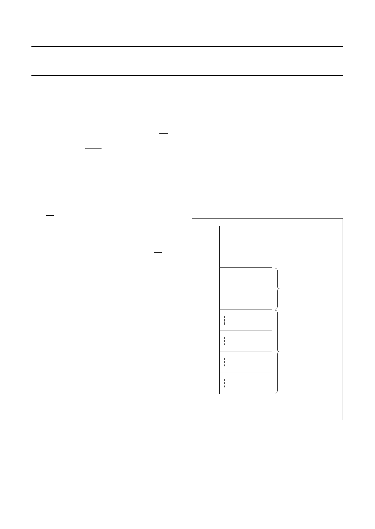
The P8xCL580 contains 256 bytes of internal RAM and
40 Special Function Registers (SFRs). Figure 6 shows the
internal Data Memory space divided into the lower
128 bytes, the upper 128 bytes, and the SFRs space.
Internal RAM locations 0 to 127 are directly and indirectly
addressable. Internal RAM locations 128 to 255 are only
indirectly addressable. The Special Function Register
locations 128 to 255 bytes are only directly addressable.
9.3 Special Function Registers (SFRs)
The upper 128 bytes are the address locations of the
SFRs. Figures 7 and 8 show the Special Function
Registers space. The SFRs include the port latches,
timers, peripheral control, serial I/O registers, etc. These
registers can only be accessed by direct addressing.
There are 128 directly addressable locations in the SFR
address space. Bit addressable SFRs are those that end
in 000B.
bit-addressable space
(bit addresses 0 to 7F)
20H
R7
R0
R7
R0
R7
R0
R7
R0
1FH
18H
17H
10H
0FH
08H
07H
4 banks of 8 registers
0
MLA560 - 1
(R0 to R7)
Fig.5 The lower 128 bytes of internal RAM.
1997 Mar 14 11

Philips Semiconductors Product specification
Low voltage 8-bit microcontrollers with
UART, I
Access to memory addressing is as follows:
• Registers in one of the four register banks through
register, direct or register-indirect
• Lower 128 bytes of internal RAM through direct or
register-indirect; upper 128 bytes of internal RAM
through direct
• Special Function Registers through direct
• External Data Memory through register-indirect
• Program Memory look-up tables through base-register
plus index-register-indirect.
andbook, full pagewidth
2
C-bus and ADC
64 kbytes
P80CL580; P83CL580
The P8xCL580 is classified as an 8-bit device since the
internal ROM, RAM, Special Function Registers,
Arithmetic Logic Unit and external data bus are all 8-bits
wide. It performs operations on bit, nibble, byte and
double-byte data types.
Facilities are available for byte transfer, logic and integer
arithmetic operations. Data transfer, logic and conditional
branch operations can be performed directly on Boolean
variables to provide excellent bit handling.
EXTERNAL
6 kbytes
6 kbytes
INTERNAL
(EA = 1)
(1) Accessible via indirect addressing only.
(2) Accessible via direct and indirect addressing.
(3) Accessible via direct addressing.
6 kbytes
PROGRAM MEMORY
EXTERNAL
(EA = 0)
255
127
OVERLAPPED SPACE
INTERNAL
DATA RAM
(1)
(2)
0
INTERNAL DATA MEMORY
SPECIAL
FUNCTION
REGISTERS
(3)
64 kbytes
MGD676
0
EXTERNAL
DATA MEMORY
Fig.6 Memory map.
1997 Mar 14 12

Philips Semiconductors Product specification
Low voltage 8-bit microcontrollers with
UART, I
2
C-bus and ADC
REGISTER
MNEMONIC
PWMP
PWM0
IP1
B
IX1
IEN1
BIT ADDRESS
FEFF FD FC FB FA F9 F8
F6F7 F5 F4 F3 F2 F1 F0
EEEF ED EC EB EA E9 E8
DIRECT
BYTE
ADDRESS (HEX)
FFHT3
FEH
FDH
FCH
F8H
F0H
EFH
EEH
EDH
ECH
EBH
EAH
E9H
E8H
P80CL580; P83CL580
ACC
S1ADR
S1DAT
S1STA
S1CON
PSW
TH2
TL2
RCAP2H
RCAP2L
T2CON
ADCH
ADCON
P4
IRQ1
E6E7 E5 E4 E3 E2 E1 E0
DEDF DD DC DB DA D9 D8
D6D7 D5 D4 D3 D2 D1 D0
CECF CD CC CB CA C9 C8
C6C7 C5 C4 C3 C2 C1 C0
E0H
DBH
DAH
D9H
D8H
D0H
CFH
CEH
CDH
CCH
CBH
CAH
C9H
C8H
C5H
C4H
C1H
C0H
MGC749
SFRs containing
directly addressable
bits
Fig.7 Special Function Register memory map (continued in Fig.8).
1997 Mar 14 13

Philips Semiconductors Product specification
Low voltage 8-bit microcontrollers with
UART, I
2
C-bus and ADC
REGISTER
MNEMONIC
IP0
P3
IEN0
BIT ADDRESS
BE BD BC BB BA B9 B8
B6B7 B5 B4 B3 B2 B1 B0
AEAF AD AC AB AA A9 A8
DIRECT
BYTE
ADDRESS (HEX)
B8H
B0H
AFH
AEH
ADH
ACH
ABH
AAH
A9H
A8H
P80CL580; P83CL580
P2
S0BUF
S0CON
P1
TH1
TH0
TL1
TL0
TMOD
TCON
PCON
DPH
DPL
SP
P0
A6A7 A5 A4 A3 A2 A1 A0
9E9F 9D 9C 9B 9A 99 98
9697 95 94 93 92 91 90
8E8F 8D 8C 8B 8A 89 88
8687 85 84 83 82 81 80
A0H
99H
98H
90H
8DH
8CH
8BH
8AH
89H
88H
87H
83H
82H
81H
80H
SFRs containing
directly addressable
bits
MLA607
Fig.8 Special Function Register memory map (continued from Fig.7).
1997 Mar 14 14

Philips Semiconductors Product specification
Low voltage 8-bit microcontrollers with
UART, I
10 I/O FACILITIES
10.1 Ports
The P8xCL580 has 40 I/O lines treated as one 8-bit port
plus 32 individually addressable bits or as five parallel 8-bit
addressable ports.
Port 4 has no alternative functions. To enable a port pin
alternative function for Ports 0, 1, 2 and 3, the port bit
latch in its SFR must contain a logic 1. The alternative
functions are detailed below:
Port 0 Provides the multiplexed low-order address and
Port 1 Used for a number of special functions:
Port 2 Provides the high-order address when expanding
Port 3 Pins can be configured individually to provide:
Each port consists of a latch (SFRs P0 to P4), an output
driver and input buffer. Ports 1, 2, 3 and 4 have internal
pull-ups (except P1.6 and P1.7). Figure 9(a) shows that
the strong transistor ‘p1’ is turned on for only 2 oscillator
periods after a LOW-to-HIGH transition in the port latch.
When on, it turns on ‘p3’ (a weak pull-up) through the
inverter. This inverter and ‘p3’ form a latch which holds the
logic 1. In Port 0 the pull-up ‘p1’ is only on when emitting
logic 1s for external memory access. Writing a logic 1 to a
Port 0 bit latch leaves both output transistors switched off
so that the pin can be used as an high-impedance input.
10.2 Port options
38 of the 40 port pins (excluding P1.6 and P1.7 with option
2S only) may be individually configured with one of the
following options. These options are also shown in Fig.9.
Option 1 Standard Port; quasi-bidirectional I/O with
2
C-bus and ADC
data bus for expanding the device with standard
memories and peripherals.
• Provides the inputs for the external interrupts:
INT2 to INT8.
• External activation of Timer 2: T2.
• External trigger of the ADC: STADC.
• The I2C-bus interface: SCL and SDA.
the device with external Program or Data Memory.
• External interrupt request inputs: INT1 andINT0.
• Counter input: T1 and T0.
• Control signals to read and write to external
memories: RD and WR.
• UART input and output: RXD and TXD.
pull-up. The strong booster pull-up ‘p1’ is turned
on for two oscillator periods after a
P80CL580; P83CL580
LOW-to-HIGH transition in the port latch;
Fig.9(a).
Option 2 Open-drain; quasi-bidirectional I/O with
n-channel open-drain output. Use as an output
requires the connection of an external pull-up
resistor; see Fig.9(b).
Option 3 Push-pull; output with drive capability in both
polarities. Under this option, pins can only be
used as outputs; see Fig.9(c).
10.3 Port 0 options
The definition of port options for Port 0 is slightly different.
Two cases are considered. First, access to external
memory (
boundary) and second, I/O accesses.
10.3.1 E
Option 1 True logic 0 and logic 1 are written as address to
Option 2 An external pull-up resistor is required for
Option 3 Not allowed for external memory accesses as
10.3.2 I/O A
Option 1 When writing a logic 1 to the port latch, the
Option 2 Open-drain; quasi-directional I/O with n-channel
Option 3 Push-Pull; output with drive capability in both
10.4 SET/RESET options
Individual mask selection of the post-reset state is
available with any of the above pins. The selection is made
by appending ‘S’ or ‘R’ to Options 1, 2, or 3 above.
Option R RESET, at reset this pin will be initialized LOW.
Option S SET, at reset this pin will be initialized HIGH.
EA = 0 or access above the built-in memory
XTERNAL MEMORY ACCESSES
the external memory (strong pull-up to be used).
external accesses.
the port can only be used as output.
CCESSES
strong pull-up ‘p1’ will be on for 2 oscillator
periods. No weak pull-up exists. Without an
external pull-up, this option can be used as a
high-impedance input.
open-drain output. Use as an output requires the
connection of an external pull-up resistor. See
Fig.9(b).
polarities. Under this option pins can only be
used as outputs. See Fig.9(c).
1997 Mar 14 15

Philips Semiconductors Product specification
Low voltage 8-bit microcontrollers with
UART, I
handbook, full pagewidth
2
C-bus and ADC
from port latch
read port pin
Q
input data
2 oscillator
periods
strong pull-up
INPUT
BUFFER
(a) Standard
P80CL580; P83CL580
+5 V
p2
p1
n
p3
I/O pin
+5 V
from port latch
read port pin
from port latch
Q
input data
Q
n
INPUT
BUFFER
(b) Open-drain
strong pull-up
+5 V
external
pull-up
I/O pin
p1
I/O pin
n
(c) Push-pull
Fig.9 Port configuration options.
1997 Mar 14 16
MGD677

Philips Semiconductors Product specification
Low voltage 8-bit microcontrollers with
UART, I
11 TIMERS/EVENT COUNTERS
The P8xCL580 contains three 16-bit timer/event counter
registers; Timer 0, Timer 1 and Timer 2 which can perform
the following functions:
• Measure time intervals and pulse durations
• Count events
• Generate interrupt requests.
In the ‘Timer’ operating mode the register is incremented
every machine cycle. Since a machine cycle consists of 12
oscillator periods, the count rate is1⁄12× f
In the ‘Counter’ operating mode, the register is
incremented in response to a HIGH-to-LOW transition.
Since it takes 2 machine cycles (24 oscillator periods) to
recognize a HIGH-to-LOW transition, the maximum count
rate is1⁄24× f
should be held for at least one complete machine cycle.
11.1 Timer 0 and Timer 1
Timer 0 and Timer 1 can be programmed independently to
operate in four modes:
Mode 0 8-bit timer or 8-bit counter each with divide-by-32
Mode 1 16-bit time-interval or event counter.
Mode 2 8-bit time-interval or event counter with automatic
Mode 3 Timer 0 establishes TL0 and TH0 as two
11.2 Timer T2
2
C-bus and ADC
. To ensure a given level is sampled, it
osc
prescaler.
reload upon overflow.
separate counters.
osc
.
P80CL580; P83CL580
11.2.1 CAPTURE MODE
Figure 10 shows the Capture mode. Two options in this
mode, may be selected by the EXEN2 bit in T2CON:
• If EXEN2 = 0, then Timer 2 is a 16-bit timer or counter
which upon overflowing sets the Timer 2 overflow bit
TF2, this may then be used to generate an interrupt.
• If EXEN2 = 1, Timer 2 operates as described above but
with the additional feature that a HIGH-to-LOW
transition at external input T2EX causes the current
value in TL2 and TH2 to be captured into registers
RCAP2L and RCAP2H respectively. In addition, the
transition at T2EX causes the EXF2 bit in T2CON to be
set; this may also be used to generate an interrupt.
11.2.2 A
Figure 11 shows the Auto-reload mode. Also two options
in this mode are selected by the EXEN2 bit in T2CON:
• If EXEN2 = 0, then when Timer 2 rolls over, it sets the
TF2 bit but also causes the Timer 2 registers to be
reloaded with the 16-bit value held in registers RCAP2L
and RCAP2H. The 16-bit value held in these registers is
preset by software.
• If EXEN2 = 1, Timer 2 operates as described above but
with the additional feature that a HIGH-to-LOW
transition at external input T2EX will also trigger the
16-bit reload and set the EXF2 bit.
11.2.3 B
The Baud Rate Generator mode is selected when
RTCLK = 1. It will be described in conjunction with the
serial port (UART); see Section 16.3.2.
UTO-RELOAD MODE
AUD RATE GENERATOR MODE
Timer T2 is a 16-bit timer/counter that can operate (like
Timer 0 and 1) either as a timer or as an event counter.
These functions are selected by the state of the C/
the T2CON register; see Tables 2 and 3.
Three operating modes are available Capture, Auto-reload
and Baud Rate Generator, which also are selected via the
T2CON register; see Table 4.
1997 Mar 14 17
T2 bit in

Philips Semiconductors Product specification
Low voltage 8-bit microcontrollers with
UART, I
handbook, full pagewidth
2
C-bus and ADC
12OSC
T2 PIN
T2EX PIN
C/T2 = 0
C/T2 = 1
transition
detector
control
TR2
capture
control
EXEN2
TL2
(8 BITS)
RCAP2L RCAP2H
TH2
(8 BITS)
P80CL580; P83CL580
TF2
Timer 2
interrupt
EXF2
MLA608
handbook, full pagewidth
T2 PIN
T2EX PIN
12OSC
C/T2 = 0
C/T2 = 1
transition
detector
Fig.10 Timer 2 in Capture mode.
TL2
(8 BITS)
control
TR2
reload
RCAP2L RCAP2H
control
EXEN2
TH2
(8 BITS)
TF2
EXF2
MLA609
Timer 2
interrupt
Fig.11 Timer 2 in Auto-Reload mode.
1997 Mar 14 18

Philips Semiconductors Product specification
Low voltage 8-bit microcontrollers with
UART, I
11.3 Timer/Counter 2 Control Register (T2CON) Table 2 Timer/Counter 2 Control Register (SFR address C8H)
76543210
TF2 EXF2 GF2 RTCLK EXEN2 TR2 C/
Table 3 Description of T2CON bits.
BIT SYMBOL DESCRIPTION
7 TF2 Timer 2 overflow flag. Set by a Timer 2 overflow and must be cleared by software. TF2
6 EXF2 Timer 2 external flag. Set when either a capture or reload is caused by a negative
5 GF2 General purpose flag bit.
4 RTCLK Receive/transmit clock flag. When set, causes the UART serial port to use Timer 2
3 EXEN2 Timer 2 external enable flag. When set, allows a capture or reload to occur as a result
2 TR2 Start/stop control for Timer 2. TR2 = 1 starts the timer.
1C/
0 CP/
2
C-bus and ADC
will not be set when RTCLK = 1.
transition on T2EX and when EXEN2 = 1. When Timer T2 interrupt is enabled,
EXF2 = 1 will cause the CPU to vector to Timer 2 interrupt routine. EXF2 must be
cleared by software.
overflow pulses for its receive and transmit clock in Modes 1 and 3. RTCLK = 0 causes
Timer 1 overflows to be used for the receive and transmit clock.
of a negative transition on T2EX, if Timer 2 is not being used to clock the serial port.
EXEN2 = 0, causes Timer 2 to ignore events at T2EX.
T2 Timer or counter select for Timer 2. C/T2 = 0 selects the internal timer with a clock
frequency of1⁄12× f
triggered.
RL2 Capture/Reload flag. When set, captures will occur on negative transitions at T2EX, if
EXEN2 = 1. When cleared, auto-reloads will occur either with Timer 2 overflows or
negative transitions at T2EX when EXEN2 = 1. When RTCLK = 1, this bit is ignored and
the timer is forced to auto-reload on a Timer 2 overflow.
. C/T2 = 1 selects the external event counter; negative edge
osc
P80CL580; P83CL580
T2 CP/RL2
Table 4 Timer 2 operating modes; X = don’t care.
RTCLK CP/
0 0 1 16-bit Auto-reload
0 1 1 16-bit Capture
1 X 1 Baud Rate Generator
XX0Off
1997 Mar 14 19
RL2 TR2 MODE

Philips Semiconductors Product specification
Low voltage 8-bit microcontrollers with
UART, I
11.4 Watchdog Timer
In addition to Timer T2 and the standard timers, a
Watchdog Timer (consisting of an 11-bit prescaler and an
8-bit timer) is also incorporated.
The Watchdog Timer is controlled by the Watchdog
Enable pin (EWN). When EWN = 0, the timer is enabled
and the Power-down mode is disabled. When EWN = 1,
the timer is disabled and the Power-down mode is
enabled. In the Idle mode the Watchdog Timer and reset
circuitry remain active.
The Watchdog Timer is shown in Fig. 12.
The timer frequency is derived from the oscillator
frequency using the following formula:
f
=
timer
2
C-bus and ADC
f
osc
-------------------------------- 12 2048×()
P80CL580; P83CL580
When a timer overflow occurs, the microcontroller is reset
and a reset output pulse is generated at the RST pin. To
prevent a system reset the timer must be reloaded in time
by the application software. If the processor suffers a
hardware/software malfunction, the software will fail to
reload the timer. This failure will produce a reset upon
overflow thus preventing the processor running out of
control.
The Watchdog Timer can only be reloaded if the condition
flag WLE (PCON.4) has been previously set by software.
At the moment the counter is loaded the condition flag is
automatically cleared.
The time interval between the timer reloading and the
occurrence of a reset is dependent upon the reloaded
value. For example, this time period may range from 2 ms
to 500 ms when using an oscillator frequency
= 12 MHz.
f
osc
handbook, full pagewidth
f
/12
osc
EWN
INTERNAL BUS
write
T3
PRESCALER
11-BIT
CLEAR
TIMER T3 (8-BIT)
LOAD
LOADEN
CLEAR
WLE PD
PCON.4
INTERNAL BUS
Fig.12 Functional diagram of the T3 Watchdog Timer.
overflow
internal
reset
LOADEN
PCON.1
V
DD
P
RST
R
RST
MGD678
1997 Mar 14 20

Philips Semiconductors Product specification
Low voltage 8-bit microcontrollers with
UART, I
12 PULSE WIDTH MODULATED OUTPUT
One Pulse Width Modulated output channel (PWM0) is
provided which outputs pulses of programmable length
and interval. The repetition frequency is defined by an 8-bit
prescaler (PWMP) that generates the clock for the
counter. The 8-bit counter counts modulo 255, i.e. from
0 to 254 inclusive. The value held in the 8-bit counter is
compared to the contents of the register PWM0.
Provided the contents of this register are greater than the
counter value, the PWM0 output is set LOW. If the
contents of register PWM0 are equal to, or less than the
counter value, the PWM0 output is set HIGH.
The pulse-width-ratio is therefore defined by the contents
of register PWM0. The pulse-width-ratio will be in the
range 0 to
of1⁄
.
255
12.1 Prescaler Frequency Control Register (PWMP) Table 5 Prescaler Frequency Control Register (address FEH)
2
C-bus and ADC
255
⁄
and may be programmed in increments
255
The repetition frequency (f
given by:
For f
frequency range of 92 Hz to 23.5 kHz.
By loading the PWM0 register with either 00H or FFH, the
PWM0 output can be retained at a constant HIGH or LOW
level respectively. When loading FFH into the PWM0
register, the 8-bit counter will never actually reach this
value.
The PWM0 output pin is driven by push-pull drivers and is
not shared with any other function.
f
PWM
P80CL580; P83CL580
) at the PWM0 output is
PWM
f
=
---------------------------------------------------------------------------2{ 1( PWMP ) 255 }×+×
= 12 MHz the above formula gives a repetition
osc
osc
76543210
PWMP.7 PWMP.6 PWMP.5 PWMP.4 PWMP.3 PWMP.2 PWMP.1 PWMP.0
Table 6 Description of PWMP bits
BIT SYMBOL DESCRIPTION
7 to 1 PWMP.7 to PWMP.0 Prescaler division factor= (PWMP) + 1.
12.2 Pulse Width Register (PWM0) Table 7 Pulse Width Register (address FCH)
76543210
PWM0.7 PWM0.6 PWM0.5 PWM0.4 PWM0.3 PWM0.2 PWM0.1 PWM0.0
Table 8 Description of PWM0 bits
BIT SYMBOL DESCRIPTION
7 to 1 PWM0.7 to PWM0.0
LOW/HIGH ratio of
PWM0 signal
=
PWM0()
-------------------------------------------------255 PWM0()–{}
1997 Mar 14 21

Philips Semiconductors Product specification
Low voltage 8-bit microcontrollers with
UART, I
handbook, full pagewidth
2
C-bus and ADC
I
N
T
E
R
N
A
L
B
U
S
f
osc
MGC750
8-BIT COMPARATOR
PRESCALER
PWMP
P80CL580; P83CL580
PWM0
OUTPUT
BUFFER
8-BIT COUNTER1/2
PWM0
Fig.13 Functional diagram of Pulse Width Modulated output (PWM0).
1997 Mar 14 22

Philips Semiconductors Product specification
Low voltage 8-bit microcontrollers with
UART, I
13 ANALOG-TO-DIGITAL CONVERTER (ADC)
The analog input circuitry consists of a 4-bit analog
multiplexer and an ADC with 8-bit resolution. The analog
reference voltage (V
connected via separate input pins. The conversion is
selectable from 24 machine cycles (24 µs at
f
= 12 MHz) to 48 machine cycles. The functional
osc
diagram of the ADC is shown in Fig. 14.
The ADC is controlled using the ADC Control Register
(ADCON). Input channels are selected by the analog
multiplexer via the ADCON register bits AADR0 and
AADR1. The completion of the 8-bit ADC conversion is
flagged by ADCI in the ADCON register and the result is
stored in the Special Function Register ADCH (address
C5H).
An ADC conversion in progress is unaffected by an
external software ADC start.
2
C-bus and ADC
) and analog ground (V
ref(p)(A)
SSA
) are
P80CL580; P83CL580
The result of a completed conversion remains unaffected
provided ADCI = 1. While ADCS = 1 or ADCI = 1, a new
ADC start will be blocked and consequently lost.
An ADC conversion already in progress is aborted when
the Power-down mode is entered. The result of a
completed conversion (ADCI = 1) remains unaffected
when entering the Idle or Power-down mode.
The analog-to-digital conversion can be started in 3 ways:
• Start in operating mode, continue in operating mode
• Start in operating mode, by setting the ADCS bit, then go
to Idle mode
• Set the ADEX bit, go to the Idle mode and start
conversion externally via the STADC pin.
For the three cases mentioned above the internal flag
ADCI is set upon completion of the conversion.
handbook, full pagewidth
ADC0
ADC1
ADC2
ADC3
(1) For the descriptions of ADCON bits see Table 10.
ADCON
(1)
ANALOG INPUT
MULTIPLEXER
START
END
8-BIT ADC
(succesive approximation)
INTERNAL BUS
STADC
ADEX
+
V
ref(p)(A)
V
SSA
12345670123456-0
ADCH
MGC751
Fig.14 Functional diagram of analog input.
1997 Mar 14 23

Philips Semiconductors Product specification
Low voltage 8-bit microcontrollers with
UART, I
13.1 ADC Control Register (ADCON) Table 9 ADC Control Register (address C4H)
76543210
−ADPD ADEX ADCI ADCS CKDIV AADR1 AADR0
Table 10 Description of ADCON bits
BIT SYMBOL DESCRIPTION
7 − Reserved.
6 ADPD Power-down. This bit switches off the resistor reference to save power even when the
5 ADEX Enable external start of conversion. This bit determines whether a conversion can be
4 ADCI ADC interrupt flag. This flag is set when an ADC conversion result is ready to be read.
3 ADCS ADC start and status flag. When this bit is set an ADC conversion is started. ADCS
2 CKDIV This bit selects the conversion time, in terms of instruction cycles. This allows the CPU
1 AADR1 Analog input select. These bits are used to select one of the four analog inputs; see
0 AADR0
2
C-bus and ADC
CPU is operating.
started using the external pin ST ADC. When ADEX = 0, a conversion cannot be started
externally using ST ADC. When ADEX= 1, a conversion can be started externally using
ST ADC.
An interrupt is invoked if this is enabled. This flag must be cleared by software (it cannot
be set by software); see Table 11.
may be set by software or by the external signal STADC. The ADC logic ensures that
this signal is HIGH while the ADC is busy. On completion of the conversion ADCS is
reset and after that the interrupt flag ADCI is set. ADCS cannot be reset by software;
see Table 11.
to be run at the maximum frequency (12 MHz) yet keeping the ADC timing at low
frequency. When CKDIV = 0, the conversion time is equivalent to 24 instruction cycles.
When CKDIV = 1, the conversion time is equivalent to 48 instruction cycles.
The conversion time includes a sampling time of 6 cycles.
Table 12. They only can be changed when ADCI and ADCS are both LOW.
P80CL580; P83CL580
Table 11 Analog-to-digital operation
ADCI ADCS OPERATION
0 0 ADC not busy; a conversion can be
started.
0 1 ADC busy; start of a new conversion is
blocked.
1 0 Conversion completed; start of a new
conversion is blocked.
1 1 Intermediate status for a maximum of
one machine cycle before conversion is
completed (ADCI = 1, ADCS = 0).
1997 Mar 14 24
Table 12 Selection of analog input channel
AADR1 AADR0 SELECTED CHANNEL
0 0 AD0
0 1 AD1
1 0 AD2
1 1 AD3
 Loading...