

Philips P87C766CBA, P87C766BDR, P83C766BDA, P83C766BDR, P83C566BDR Datasheet
...
DATA SH EET
Product specification
File under Integrated Circuits, IC20
1999 Mar 10
INTEGRATED CIRCUITS
P8xCx66 family
Microcontrollers for PAL/SECAM
TV with OSD and VST

1999 Mar 10 2
Philips Semiconductors Product specification
Microcontrollers for PAL/SECAM TV
with OSD and VST
P8xCx66 family
CONTENTS
1 FEATURES
2 GENERAL DESCRIPTION
3 ORDERING INFORMATION
4 BLOCK DIAGRAM
5 PINNING INFORMATION
6 MEMORY ORGANIZATION
7 I/O FACILITY
8 TIMERS AND EVENT COUNTERS
9 REDUCED POWER MODE
10 I2C-BUS SERIAL I/O
11 INTERRUPT SYSTEM
12 OSCILLATOR CIRCUITRY
13 RESET CIRCUITRY
14 PIN FUNCTION SELECTION
15 ANALOG CONTROL
16 ANALOG-TO-DIGITAL CONVERTERS (ADC)
17 ON-SCREEN DISPLAY (OSD)
18 EPROM PROGRAMMER
19 SPECIAL FUNCTION REGISTERS
ADDRESS MAP
20 LIMITING VALUES
21 CHARACTERISTICS
22 PINNING CHARACTERIZATION
23 PACKAGE OUTLINES
24 SOLDERING
25 DEFINITIONS
26 LIFE SUPPORT APPLICATIONS
27 PURCHASE OF PHILIPS I2C COMPONENTS

1999 Mar 10 3
Philips Semiconductors Product specification
Microcontrollers for PAL/SECAM TV
with OSD and VST
P8xCx66 family
1 FEATURES
1.1 P80C51 CPU core
• 80C51 8-bit CPU
• 64-kbyte Multiple Programming ROM (MTP ROM)
• Two 16-bit timer/event counters
• Crystal oscillator for system clock (up to 12 MHz)
• 12 source, 12 vector interrupt structure with two priority
levels
• Enhanced architecture with:
– Non-page orientated instructions
– Direct addressing
– Four 8-byte RAM register banks
– Stack depth up to 128 bytes
– Multiply, divide, subtract and compare instructions.
1.2 P8xCx66 family
• ROM/RAM: see Table 1
• Pulse Width Modulated (PWM) outputs:
– One 14-bit PWM output for Voltage Synthesized
Tuning (VST)
– Eight 7-bit PWM outputs for analog controls.
• 3 Analog-to-Digital (ADC) inputs with 4-bit DAC and
comparator
• LED driver port:
– All I/O port lines with 10 mA LED drive capability
(V
O
<1.0 V)
– Up to 5 LEDs can be driven at any one time.
• Serial I/O:
– Multi-master I2C-bus interface
– Maximum I2C-bus frequency 400 kHz.
• Watchdog timer
• Improved EMC measures and slope controlled I/Os
• OSD functions:
– Programmable VSYNC and HSYNC active levels
– Display RAM: 192 × 12 bits
– Display character fonts: 128 (126 customer fonts plus
2 reserved codes)
– 63 vertical starting positions controlled by software
– 110 horizontal starting positions controlled by
software
– Character size: 4 different character sizes on a
line-by-line basis
– Character matrix: 12 × 18 with no spacing between
characters
– Foreground colours: 8 on a character-by-character
basis
– Background/shadowing modes: two primary modes -
TV mode and Frame mode on a frame basis. Each
primary mode has four sub-modes on a line basis:
Sub-mode 1: Superimpose (no background)
Sub-mode 2: North-West shadowing
Sub-mode 3: Box background
Sub-mode 4: Border shadowing
– Background colours: 8 on a word-by-word basis,
available in all four sub-modes
– Display RAM starting address is programmable; fast
switching between banks of display (RAM)
characters is possible through software control
– HSYNC driven PLL for OSD clock (4 to 12 MHz)
– Character blinking ratio: 1 : 1
– Character blinking frequency: programmable using
f
VSYNC
divisors of 32 and 64, on a character basis
– Flexible display format using the Carriage Return
code and the Space codes
– Display RAM address post incremented each time
new data is written into RAM
– Vertical jitter cancelling circuit to avoid unstable
VSYNC leading edge mismatch with HSYNC signal
– OSD meshing.
• Power-on reset
• Packages: SDIL42 (PLCC68 for piggy-back only)
• Operating voltage: 4.5 to 5.5 V
• Operating temperature: −20 to +70 °C
• System clock frequency: 4 to 12 MHz
• OSD clock frequency: 4 to 12 MHz.

1999 Mar 10 4
Philips Semiconductors Product specification
Microcontrollers for PAL/SECAM TV
with OSD and VST
P8xCx66 family
2 GENERAL DESCRIPTION
The P8xCx66 family consists of the following devices:
• P83C266
• P83C366
• P83C566
• P83C766
• P87C766.
The P8xCx66 family are 80C51-based microcontrollers
designed for medium-high to high-end TV control
applications. The P8xCx66 devices incorporate many
unique features on-chip, giving them a competitive edge
over similar devices from other manufacturers.
The Philips 80C51 CPU is object code compatible with the
industry standard 80C51. All devices are manufactured in
an advanced CMOS technology.
The P8xCx66 family also function as arithmetic processors
having facilities for both binary and BCD arithmetic plus bit
handling capabilities. The instruction set consists of over
100 instructions: 49 one-byte, 46 two-byte and
16 three-byte. Multiply and divide instructions are
implemented by hardware with a cycle time of 4 µs
(f
CLK
= 12 MHz).
The term P8xCx66 is used throughout this data sheet to
refer to all family members; differences between devices
are highlighted in the text.
Table 1 Memory structure for the different family members
3 ORDERING INFORMATION
MEMORY P83C266 P83C366 P83C566 P83C766 P87C766
ROM 24 kbytes 32 kbytes 48 kbytes 64 kbytes −
RAM 512 bytes 512 bytes 1 kbyte 1 kbyte 2 kbytes
EPROM −−−−64 kbytes
Main memory 256 bytes 256 bytes 256 bytes 256 bytes 256 bytes
Auxiliary RAM 256 bytes 256 bytes 768 bytes 768 bytes 1792 bytes
TYPE NUMBER
PACKAGE
NAME DESCRIPTION VERSION
P83C266BDR SDIP42 plastic shrink dual in-line package; 42 leads (600 mil) SOT270-1
P83C366BDR
P83C366CBP
P83C566BDR
P83C766BDP
P87C766BDR
P87C766CBP
P83C366BDA PLCC68 plastic leaded chip carrier; 68 leads SOT188-2
P83C566BDA
P83C766BDA
P87C766CBA
1999 Mar 10 5
Philips Semiconductors Product specification
Microcontrollers for PAL/SECAM TV
with OSD and VST
P8xCx66 family
This text is here in white to force landscape pages to be rotated correctly when browsing through the pdf in the Acrobat reader.This text is here in
_white to force landscape pages to be rotated correctly when browsing through the pdf in the Acrobat reader.This text is here inThis text is here in
white to force landscape pages to be rotated correctly when browsing through the pdf in the Acrobat reader. white to force landscape pages to be ...
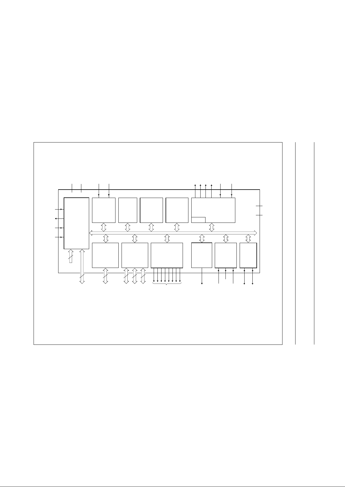
4 BLOCK DIAGRAM
o
ok, full pagewidth
MGL302
6
6
8-bit internal bus
8-BIT
WATCHDOG
TIMER
(T3)
ROM
32 KBYTES
(1)
OR
EPROM
64 KBYTES
(2)
RAM
512 BYTES
(1)
OR
2 KBYTES
(2)
8 × 7-BIT
DACS
3 × 4-BIT
ADCS
14-BIT DAC
ON SCREEN DISPLAY
(OSD)
PLL
P0
internal
interrupts
external
interrupts
8
P1
8
P5
PWM0 to PWM7
(4)
V
PP
RESET
I2C-BUS
INTERFACE
ADC1
(5)
ADC2
(5)
ADC0
(5)
SDA
(3)
SCL
(3)
TWO 16-BIT
TIMER/
COUNTERS
(T0 AND T1)
T0
(3)
T1
(3)
V
SSD
V
DDD
FUNCTION
COMBINED
PARALLEL
I/O PORTS
PARALLEL
I/O PORT
CPU
80C51 CORE
EXCLUDING
ROM/RAM
XTALIN
XTALOUT
TPWM
(4)
RB GFB HSYNC
P8xCx66
VSYNC
V
DDA
V
SSA
8 4
P3
Fig.1 P83C366 and P87C766 block diagram.
(1) For the P83C366.
(2) For the P87C766.
(3) Alternative functions of Port 1.
(4) Alternative functions of Port 5, except PWM7 which is an alternative function of Port 3.
(5) Alternative functions of Port 3.
1999 Mar 10 6
Philips Semiconductors Product specification
Microcontrollers for PAL/SECAM TV
with OSD and VST
P8xCx66 family
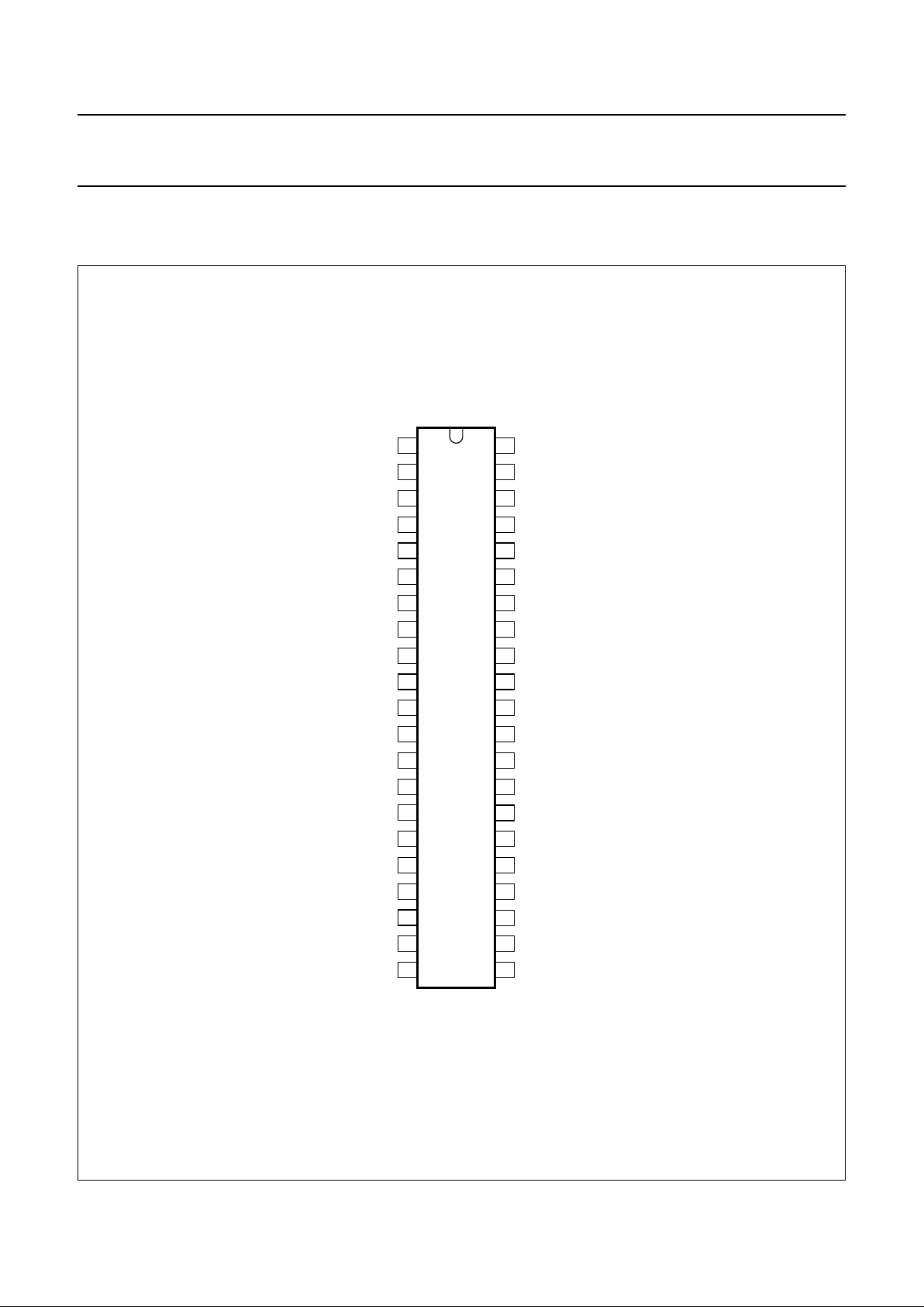
5 PINNING INFORMATION
5.1 Pinning
Fig.2 Pin configuration (SDIP42).
handbook, halfpage
P8xCx66
MGL301
1
2
42
41
3
4
5
6
7
8
9
10
11
12
13
14
15
16
17
18
19
20
40
39
38
37
36
35
34
33
32
31
30
29
28
27
26
25
24
23
2221
V
DDD
P1.7
P1.6/SDA
P1.5/SCL
P1.4/T1
P1.3/INT0
P1.2/T0
P1.1/INT1
P1.0
RESET
XTALOUT
XTALIN
V
PP
V
SSA
V
DDA
VSYNC
HSYNC
FB
R
G
B
P5.0/TPWM
P5.1/PWM0
P5.2/PWM1
P5.3/PWM2
P5.4/PWM3
P5.5/PWM4
P5.6/PWM5
P5.7/PWM6
P3.0/ADC0
P3.1/ADC1
P3.2/ADC2
P3.3/PWM7
P0.0
P0.1
P0.2
P0.3
P0.4
P0.5
P0.6
P0.7
V
SSD
1999 Mar 10 7
Philips Semiconductors Product specification
Microcontrollers for PAL/SECAM TV
with OSD and VST
P8xCx66 family
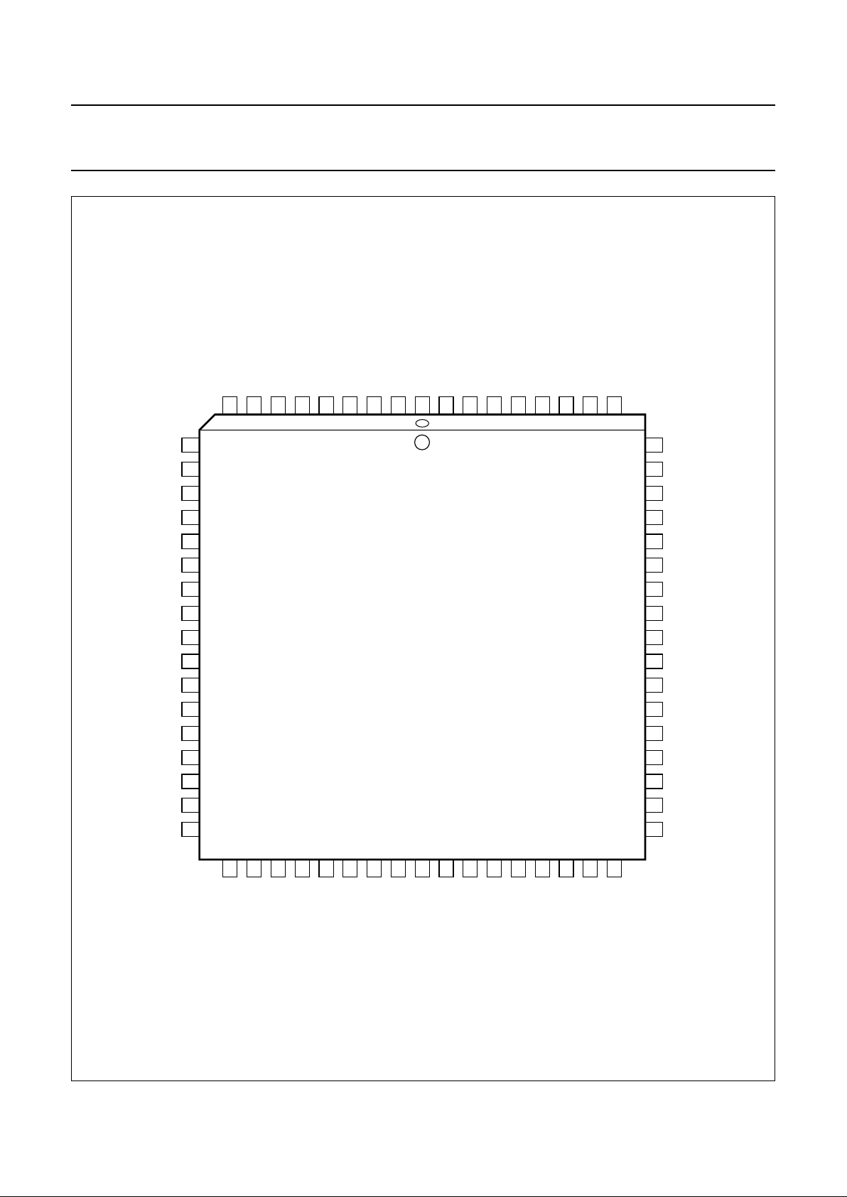
Fig.3 Pin configuration (PLCC68).
handbook, full pagewidth
P87C766
MGL329
10
11
12
13
14
15
16
17
18
19
20
21
22
23
24
25
26
n.c.
P5.6/PWM5
P5.7/PWM6
P3.0/ADC0
PH1SEM
S1ESEM
P3.1/ADC1
P2.0
P3.2/ADC2
P2.1
P3.3/PWM7
P2.2
P2.3
P0.0
P0.1
P0.2
OSD_EPR_TST
n.c.
P1.2/T0
P1.1/INT1
P1.0
V
SS
EMUPBX
RESET
IDLPDEM
P2.7
XTALOUT
XTALIN
V
SS
V
PP
P2.6
V
SSA
V
DDA
n.c.
60
59
58
57
56
55
54
53
52
51
50
49
48
47
46
45
44
27
28
29
30
31
32
33
34
35
36
37
38
39
40
41
42
43
n.c.
P0.3
P0.4
P0.5
P0.6
P0.7
V
DDD
V
SS
P2.4
P2.5
B
G
R
FB
HSYNC
VSYNC
n.c.
n.c.
P5.5/PWM4
P5.4/PWM3
P5.3/PWM2
P5.2/PWM1
P5.1/PWM0
P5.0/TPWM
INTD
VSSV
DDD1VSSD1
P1.7
P1.6/SDA
P1.5/SCL
P1.4/T1
P1.3/INT0
n.c.
9
8
7
6
5
4
3
2
1
68
67
66
65
64
63
62
61
1999 Mar 10 8
Philips Semiconductors Product specification
Microcontrollers for PAL/SECAM TV
with OSD and VST
P8xCx66 family
5.2 Pin description
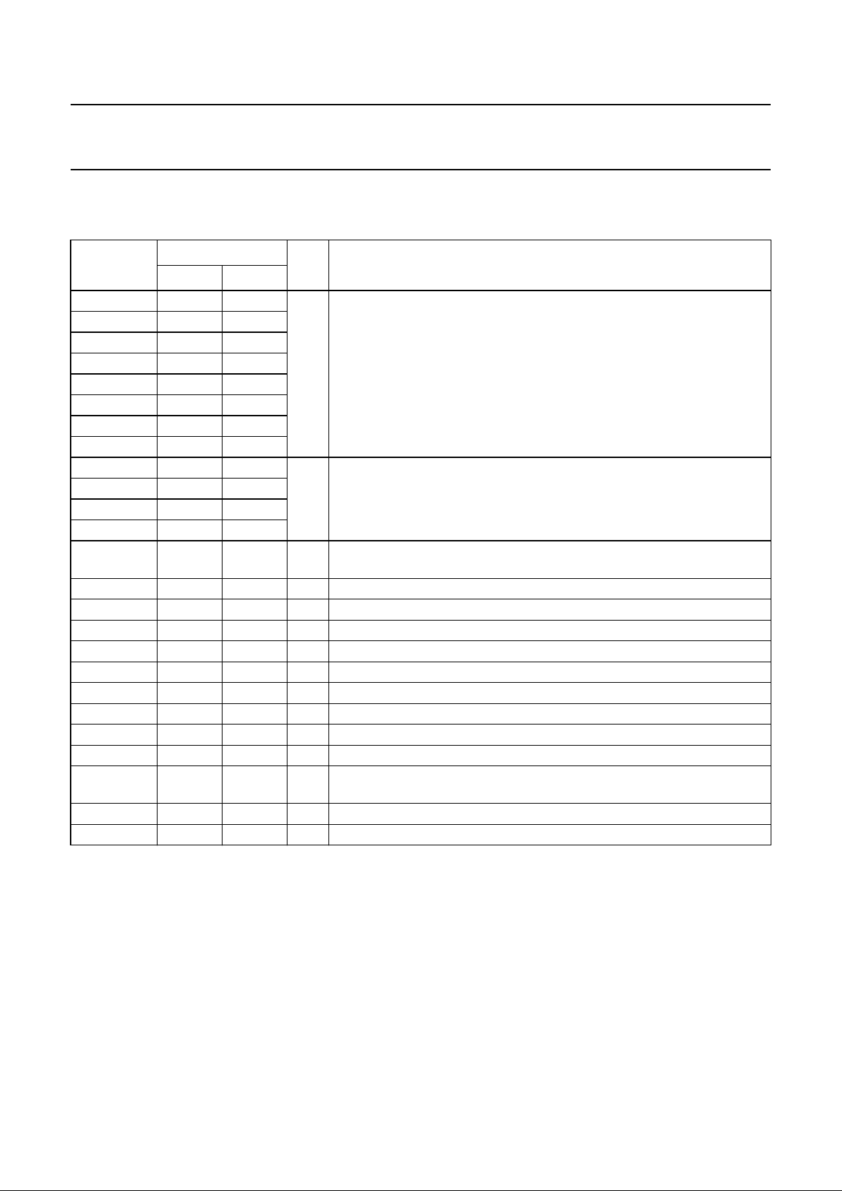
Table 2 Pin description for SDIP42 and PLCC68 packages
SYMBOL
PIN
I/O DESCRIPTION
SDIP42 PLCC68
P5.0/TPWM 1 3 I/O Port 5: 8-bit open-drain, bidirectional port.(P5.0 to P5.7) with 8 alternative
functions.
TWPM: 14-bit PWM output.
PWM0 to PWM6: 7-bit PWM outputs.
P5.1/PWM0 2 4
P5.2/PWM1 3 5
P5.3/PWM2 4 6
P5.4/PWM3 5 7
P5.5/PWM4 6 8
P5.6/PWM5 7 11
P5.7/PWM6 8 12
P3.0/ADC0 9 13 I/O Port 3: 4-bit open-drain, bidirectional port.(P3.0 to P3.3) with 4 alternative
functions.
ADC0 to ADC2: ADC inputs.
PWM7: 7-bit PWM output.
P3.1/ADC1 10 16
P3.2/ADC2 11 18
P3.3/PWM7 12 20
P0.0 to P0.7 13 to 20 23 to 25,
28 to 32
I/O Port 0: 8-bit open-drain, bidirectional port (P0.0 to P0.7).
V
SSD
21 − Ground line for digital circuits.
B 22 37 O OSD blue colour output.
G 23 38 O OSD green colour output.
R 24 39 O OSD red colour output.
FB 25 40 O OSD fast blanking output.
HSYNC 26 41 I TV horizontal sync Schmitt trigger input (for OSD synchronization).
VSYNC 27 42 I TV vertical sync Schmitt trigger input (for OSD synchronization).
V
DDA
28 45 − 5 V analog power supply.
V
SSA
29 46 − Ground line for analog circuits.
V
PP
30 48 I +12.75 V programming voltage supply (OTP) for EPROM only. 0 V in
normal application. For the ROM version this pin is not connected.
XTALIN 31 50 I Crystal input.
XTALOUT 32 51 O Crystal output.

1999 Mar 10 9
Philips Semiconductors Product specification
Microcontrollers for PAL/SECAM TV
with OSD and VST
P8xCx66 family
RESET 33 54 I Reset input.
P1.0 34 57 I/O Port 1: 8-bit open-drain, bidirectional port (P1.0 to P1.7) with 6 alternative
functions.
INT1 and INT0: external interrupts 1 and 0.
T1 and T0: 16-bit timer/counter 1 and 0 inputs
SCL: I
2
C-bus clock line
SDA: I2C-bus data line
P1.1/INT1 35 58
P1.2/T0 36 59
P1.3/INT0 37 62
P1.4/T1 38 63
P1.5/SCL 39 64
P1.6/SDA 40 65
P1.7 41 66
V
DDD
42 33 − 5 V digital power supply.
V
SS
− 1, 49, 56 − Ground lines.
n.c. − 9, 10, 27,
43, 44,
60, 61
− not connected
INTD − 2 I These 3 signals are used for metalink+ emulation.
PH1SEM − 14 I/O
S1ESEM − 15 I/O
P2.0 − 17 I/O Port 2: 8-bit open-drain, bidirectional port (P2.0 to P2.7).
P2.1 − 19
P2.2 − 21
P2.3 − 22
P2.4 − 35
P2.5 − 36
P2.6 − 47
P2.7 − 52
OSD_EPR_
TST
− 26 I/O OSD EPROM test enable.
IDLPDEM − 53 I/O These 2 signals are used for metalink+ emulation.
EMUPBX − 55 I/O
V
SSD1
− 67 − Ground line for digital circuits.
V
DDD1
− 68 − 5 V digital power supply.
SYMBOL
PIN
I/O DESCRIPTION
SDIP42 PLCC68

1999 Mar 10 10
Philips Semiconductors Product specification
Microcontrollers for PAL/SECAM TV
with OSD and VST
P8xCx66 family
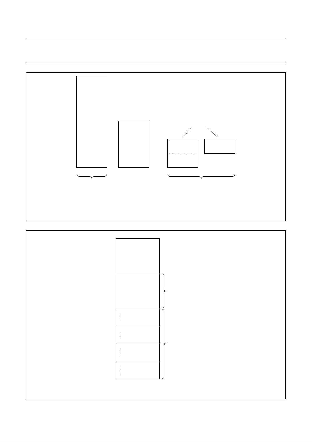
6 MEMORY ORGANIZATION
The P8xCx66 family provides 24, 32, 48 or 64 kbytes of
program memory (ROM/EPROM) plus 512, 1024 or
2048 bytes of data memory (RAM) on-chip (see Table 1).
The device has separate address spaces for program and
data memory (see Fig.4). These devices have no external
memory access capability as the RD (read), WR (write),
EA (External Access), PSEN (read strobe) and ALE
(Address Latch Enable) signals are not bonded out.
6.1 Data memory
The P8xCx66 family contains 512, 1024 or 2048 bytes of
internal RAM and 56 Special Function Registers (SFRs).
Figure 4 shows the internal data memory space divided
into the lower 128, the upper 128, AUX-RAM and the SFR
space. The lower 128 bytes of internal RAM are organized
as shown in Fig.5. The lowest 32 bytes are grouped into
4 banks of 8 registers. Program instructions refer to these
registers as R0 to R7. Two bits in the Program Status
Word (PSW) select which register bank is in use. The next
16 bytes above the register bank form a block of
bit-addressable memory space. The 128 bits in this area
can be directly addressed by the single-bit manipulation
instructions. The remaining registers (30H to 7FH) are
directly and indirectly byte addressable. The registers that
reside at addresses above 7FH and up to FFH can only be
accessed indirectly. These register addresses overlap the
SFR addresses as described in Section 6.2.
6.2 Special Function Registers
The upper 128 bytes are the address locations of the
SFRs when accessed directly. SFRs include the port
latches, timers, 7-bit PWMs, 14-bit VST PWM, ADCs and
OSD control registers. These registers can only be
accessed by direct addressing. There are
128 bit-addressable locations in the SFR address space
(SFRs with addresses divisible by eight). Their addresses
are a multiple of 08H, from 80H to F8H. (i.e., 80H, 88H,
90H, 98H etc.). See Chapter 19 for SFR list.
6.3 AUX RAM
The 1792 byte (P87C766) or 768 byte (P83C766)
AUX RAM, while physically located on-chip, logically
occupies the first 1792/768 bytes of external data memory.
As such, it is indirectly addressed in the same way as
external data memory using MOVX instructions in
combination with any of the registers R0, R1 or DPTR.
6.4 Addressing
The P80C51 CPU has five methods for addressing source
operands
• Register
• Direct
• Register-indirect
• Immediate
• Base-register-plus index-register-indirect.
The first three methods can be used for addressing
destination operands. Most instructions have a
‘destination/source’ field that specifies the data type,
addressing methods and operands involved.
For operations other than MOVs, the destination operand
is also a source operand.
Access to memory addressing is as follows:
• Registers in one of the four register banks through
register direct or indirect
• Internal RAM (128 bytes) through direct or
register-indirect
• Special Function Registers through direct
• External data memory through register-indirect
(for AUX RAM)
• Program memory look-up tables through
base-register-plus index-register-indirect.
1999 Mar 10 11
Philips Semiconductors Product specification
Microcontrollers for PAL/SECAM TV
with OSD and VST
P8xCx66 family
Fig.4 Memory map.
(1) For the P83C766 and the P87C766.
(2) For the P87C766.
(3) For the P83C566 and the P83C766.
handbook, full pagewidth
MGM680
INTERNAL
DATA RAM
AUX RAM
1792 BYTES
(2)
OR
768 BYTES
(3)
64 KBYTES
(1)
255
127
0
INTERNAL DATA MEMORY
OVERLAPPED SPACE
INTERNAL
PROGRAM MEMORY
0
SPECIAL
FUNCTION
REGISTERS
Fig.5 The lower 128 bytes of internal RAM.
handbook, halfpage
MGM677
R7
R0
07H
0
R7
R0
0FH
08H
R7
R0
17H
10H
R7
R0
1FH
18H
2FH
7FH
20H
30H
bit-addressable space
(bit addresses 00H to 7FH)
4 banks of 8 registers
(R0 to R7)

1999 Mar 10 12
Philips Semiconductors Product specification
Microcontrollers for PAL/SECAM TV
with OSD and VST
P8xCx66 family
7 I/O FACILITY
7.1 I/O ports
The SDIP42 package has 28 I/O lines treated as
28 individual addressable bits or as 3 parallel 8-bit
addressable ports (Ports 0, 1 and 5) and one 4-bit port
(Port 3).
When these 28 I/O lines are used as input ports, the
corresponding bits in SFRs P0, P1, P3 and P5 should be
set to a logic 1 to facilitate the external input signal.
Ports 1, 3 and 5 also perform the following alternative
functions.
Port 1. Used for a number of special functions:
• Provides the external interrupt inputs (INT0 and INT1)
• Provides the 16-bit timer/counter inputs (T0 and T1)
• Provides the I
2
C-bus data and clock signals (SDA and
SCL)
• P1.0 and P1.7 can be used as external interrupt inputs.
Port 3. Only 4 lines available for alternative functions:
• 7-bit PWM output (PWM7)
• ADC inputs ADC0 to ADC2.
Port 5.
• Provides the 14-bit PWM output (TPWM)
• 7-bit PWMs outputs (PWM0 to PWM6).
To enable the alternative functions of Ports 1, 3 and 5, the
port bit latch of its associated SFR must contain a logic 1.
Each port consists of a latch (SFRs P0, P1, P3 and P5), an
output driver and an input buffer.
7.2 Port configurations
1. Open-drain quasi-bidirectional I/O with n-channel
pull-down (see Fig.6). Use as an output requires the
connection of an external pull-up resistor. Use as an
input requires to write a logic 1 to the port latch before
reading the port line.
2. Push-pull; gives drive capability of the output in both
polarities, see Fig.7.
Fig.6 Open-drain port.
handbook, halfpage
MGK547
n
Q
from port latch
input data
read port pin
INPUT
BUFFER
I/O pin
Fig.7 Push-pull port.
handbook, halfpage
MGM679
p1
n
strong pull-up
+5 V
Q
from port latch
output pin

1999 Mar 10 13
Philips Semiconductors Product specification
Microcontrollers for PAL/SECAM TV
with OSD and VST
P8xCx66 family
8 TIMERS AND EVENT COUNTERS
The P8xCx66 contains two 16-bit timers/counters: Timer 0
and Timer 1 and also an 8-bit Watchdog timer.
8.1 16-bit timer/counters (T0 and T1)
Timer 0 and Timer 1 perform the following functions:
• Measure time intervals and pulse durations
• Count events
• Generate interrupt requests.
Timer 0 and Timer 1 can be independently programmed to
operate in one of four modes.
Mode 0 8-bit timer or counter with divide-by-32 prescaler.
Mode 1 16-bit time-interval or event counter.
Mode 2 8-bit time-interval or event counter with automatic
reload upon overflow.
Mode 3 Timer 0 establishes TL0 and TL1 as two
separate counters.
In the ‘timer’ function, the register is incremented every
machine cycle. Since a machine cycle consists of
12 oscillator periods, the count rate is
1
⁄12f
osc
.
In the ‘counter’ function, the register is incremented in
response to a HIGH-to-LOW transition. Since it takes
2 machine cycles (24 oscillator periods) to recognize a
HIGH-to-LOW transition, the maximum count rate is
1
⁄24f
osc
. To ensure that a given level is sampled, it should
be held for at least one complete machine cycle.
8.2 Watchdog timer (T3)
In addition to the standard timers, a Watchdog timer is
implemented on-chip. The Watchdog timer generates a
hardware reset upon overflow. In this way a
microcontroller system can recover from erroneous
processor states caused by electrical noise, RFI or
unexpected ROM code behaviour.
The Watchdog timer consists of an 8-bit timer with an
11-bit prescaler as shown in Fig.8. The prescaler input
frequency is
1
⁄12f
osc
. The 8-bit timer is incremented every
‘t’ seconds where ‘t’ is calculated as shown below:
The 8-bit timer is an up-counter so a value 00H gives the
maximum timer interval (510 ms at 12 MHz, 1536 ms at
4 MHz), and a value of FFH gives the minimum timer
interval (2 ms at 12 MHz, 6 ms at 4 MHz). When the 8-bit
timer produces an overflow a short internal reset pulse is
generated which will reset the P8xCx66.
The timer has no disable function. Consequently, all
applications must reload the timer within the previously
loaded timer interval otherwise a reset will occur. The timer
is not stopped in the Idle mode. The interrupt routine for
the Idle mode should also service the Watchdog timer.
The Watchdog timer is controlled by the WLE bit in the
Power Control Register (see Section 9.6). The WLE bit
must be set by the Watchdog timer service routine before
the timer interval can be loaded into T3. A load of T3
automatically clears the WLE bit.
A system reset clears the Watchdog timer and the
prescaler.
8.2.1 W
ATCHDOG TIMER REGISTER (WDT)
Table 3 Watchdog timer Register (SFR address FFH)
76543210
T37 T36 T35 T34 T33 T32 T31 T30
t 12 2048×
1
f
osc
--------
×=
1999 Mar 10 14
Philips Semiconductors Product specification
Microcontrollers for PAL/SECAM TV
with OSD and VST
P8xCx66 family
Fig.8 Block diagram of the Watchdog timer.
ndbook, full pagewidth
MGL298
INTERNAL BUS
1/12 f
osc
PRESCALER
11-BIT
WDT REGISTER
(8-BIT)
LOADCLEAR LOADEN
write T3
LOADEN
PCON.4
PCON.0
CLEAR
WLE IDL
internal reset
INTERNAL BUS
RESET
R
RESET

1999 Mar 10 15
Philips Semiconductors Product specification
Microcontrollers for PAL/SECAM TV
with OSD and VST
P8xCx66 family
9 REDUCED POWER MODE
Only one reduced power mode is implemented; this is the
Idle mode.
During Idle mode all blocks are inactive except Timer 0,
Timer 1, INT0, INT1 and the Watchdog timer. These active
functions may generate an interrupt (if their interrupts are
enabled) and this will cause the device to leave the Idle
mode.
The Idle mode is activated by software using the PCON
register; this register is described in Section 9.6.
9.1 Idle mode
The instruction that sets PCON.0 is the last instruction
executed before entering the Idle mode. Once in the Idle
mode, the internal clock is gated away from the CPU and
from all derivative functions (PWM/TPWM/ADC/I
2
C-bus),
except Timer 0, Timer 1 and interrupts INT0 and INT1.
The Watchdog timer remains active. The CPU status is
preserved along with the Stack Pointer, Program Counter,
Program Status Word and the Accumulator. The RAM and
all other registers maintain their data during Idle mode and
the port pins retain the logic states held at Idle mode
activation. The OSD clock is gated away from OSD circuit
in Idle mode.
9.2 Recover from Idle mode
There are 3 methods used to terminate the Idle mode.
9.2.1 V
IA AN INTERRUPT
Activation of INT0, INT1 or an interrupt from Timer 0 or
Timer 1 will cause PCON to be cleared by hardware thus
terminating the Idle mode. The interrupt is serviced and
following the RETI instruction, the next instruction to be
executed will be the one following the instruction that put
the device in the Idle mode. All the other interrupts are
disabled and will not generate an interrupt to wake-up the
CPU.
9.2.2 V
IA RESET
The second method of terminating the Idle mode is with an
external hardware reset. Since the oscillator is still
running, the hardware reset is required to be active for only
two machine cycles to complete the reset operation. Reset
redefines all SFRs, but does not effect the on-chip RAM.
9.2.3 V
IA A WATCHDOG TIMER OVERFLOW
If the Watchdog timer is allowed to overflow or an
erroneous processor state causes an overflow, a
hardware reset will be generated, thus terminating the Idle
mode.
9.3 General purpose flags (GF0 and GF1)
Flags GF0 and GF1 may be used to determine whether
the interrupt was received during normal execution or Idle
mode. For example, the instruction that writes to PCON.0
to set the Idle mode can also set or clear one or both flags.
When the Idle mode is terminated by an interrupt, the
service routine can examine the status of the flag bits.
9.4 Output in Idle mode
• Ports will keep the value they had before entering the
Idle mode
• The PWM0 to PWM7 outputs will be LOW
• The TPWM output will be LOW
• The I
2
C-bus output is HIGH
• The pins R, G, B and FB will be the ‘inverse of Bp’,
(defined by bit 2 of SFR OSCON).
9.5 Pending interrupts in Idle mode
If pending interrupts (I
2
C-bus, VSYNC, P1.0 to P1.4 or
P1.7) are present at the moment the CPU is switched to
Idle mode, then these interrupts will wake-up the CPU.
If this is not wanted then before entering the Idle mode all
interrupts must be disabled, except those interrupts
allowed to wake-up the CPU (INT0, INT1, Timer 0 and
Timer1). New interrupts from I2C-bus, VSYNC,
P1.0 to P1.4 or P1.7 are disabled as soon as Idle mode is
entered.
For example if a high priority interrupt is serviced just
before the instruction which sets PCON.0 and a lower
priority interrupt is generated during the interrupt service
routine of the high priority interrupt, then the lower priority
interrupt is pending. After the high priority interrupt is
serviced (last instruction of routine is RETI) the main
program will execute at least one more instruction to
prevent a deadlock of the main program. In this case, it is
the instruction which sets the PCON.0 bit (enter Idle
mode). The pending lower level interrupt will, if enabled,
immediately wake-up the CPU for an interrupt service,
even though this interrupt is not INT0, INT1 or an interrupt
from Timer 1 or Timer 0.
1999 Mar 10 16
Philips Semiconductors Product specification
Microcontrollers for PAL/SECAM TV
with OSD and VST
P8xCx66 family
9.6 Power Control Register (PCON)
PCON is byte addressable only.
Table 4 Power Control Register (SFR address 87H)
Table 5 Description of PCON bits
76543210
−−−WLE GF1 GF0 0 IDL
BIT SYMBOL DESCRIPTION
7 − These 3 bits are reserved.
6 −
5 −
4 WLE Watchdog Load Enable. If WLE = 1, the Watchdog timer can be loaded. If WLE = 0,
the Watchdog timer cannot be loaded.
3 GF1 General purpose flag 1.
2 GF0 General purpose flag 0.
1 − This bit is reserved and must be set to a logic 0.
0 IDL Idle mode select. If IDL = 1, the Idle mode is selected. If IDL = 0, the Idle mode is
inhibited, i.e. normal operation.
1999 Mar 10 17
Philips Semiconductors Product specification
Microcontrollers for PAL/SECAM TV
with OSD and VST
P8xCx66 family
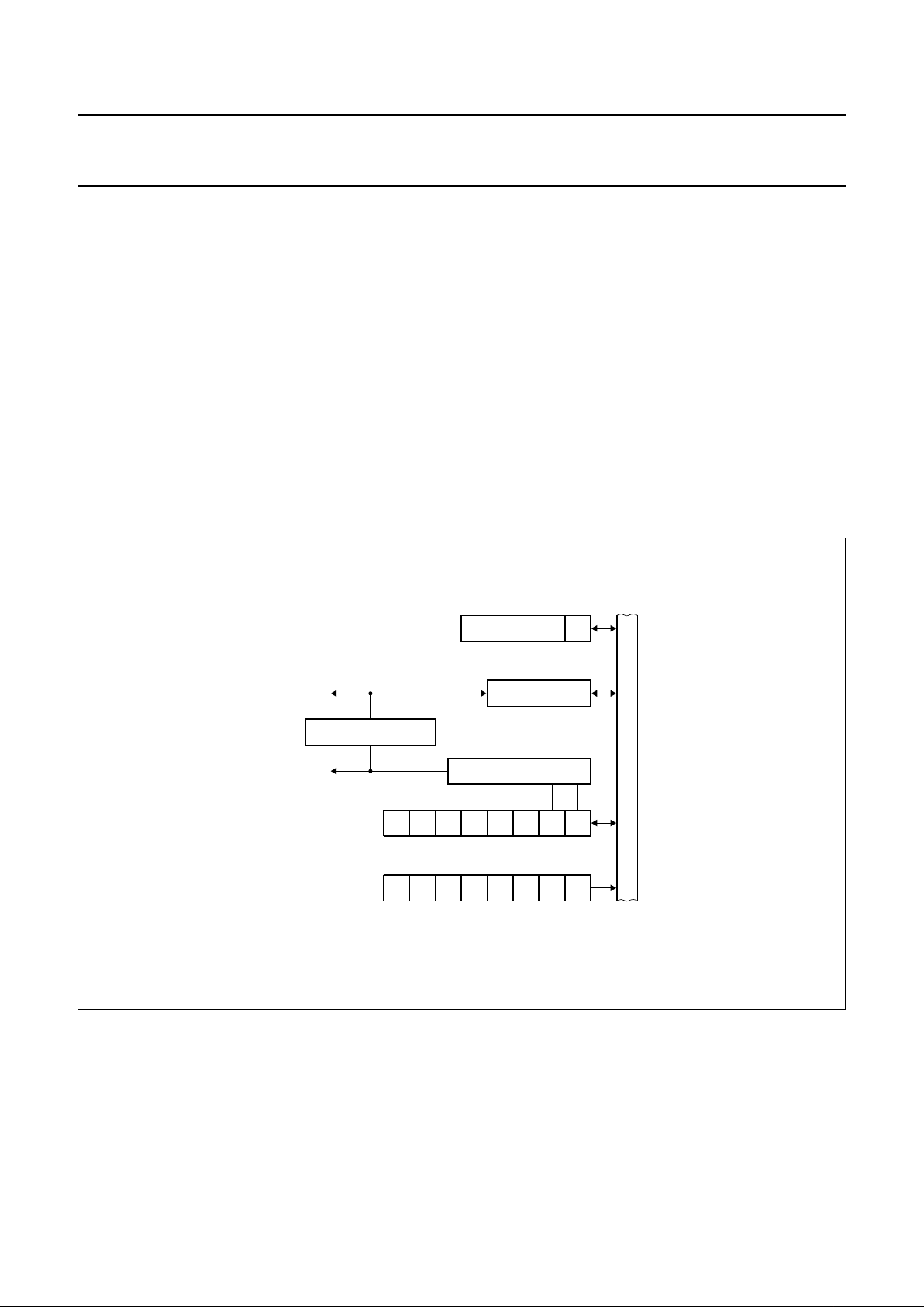
10 I2C-BUS SERIAL I/O
10.1 The I
2
C-bus
The serial port supports the two line I2C-bus. The I2C-bus
consists of a serial data line (SDA) and a serial clock line
(SCL). These lines can also function as I/O port lines
P1.6 and P1.5 respectively. To utilize this facility pins
P1.5/SCL and P1.6/SDA must be configured as alternative
functions instead of port lines; see Section 10.8.
The system is unique because data transport, clock
generation, address recognition and bus control arbitration
are all controlled by hardware.
Full details of the I2C-bus are given in the document
“The I2C-bus and how to use it”
. This document may be
ordered using the code 9398 393 40011.
10.2 Operation modes
The I
2
C-bus serial I/O has complete autonomy in byte
handling and operates in four modes
• Master transmitter
• Master receiver
• Slave transmitter
• Slave receiver.
These functions are controlled by the S1CON register.
S1STA is the status register whose contents may also be
used as a vector to various service routines. S1DAT is the
data shift register and S1ADR the slave address register.
Slave address recognition is performed by hardware.
Fig.9 Block diagram of I2C-bus serial I/O.
handbook, full pagewidth
MBC749 - 1
SLAVE ADDRESS
S1ADR
GC
SHIFT REGISTER
S1DAT
SDA
ARBITRATION LOGIC
SCL BUS CLOCK GENERATOR
S1STA
INTERNAL BUS
76543210
S1CON
76543210

1999 Mar 10 18
Philips Semiconductors Product specification
Microcontrollers for PAL/SECAM TV
with OSD and VST
P8xCx66 family
10.3 Serial Control Register (S1CON)
Table 6 Serial Control Register (SFR address D8H)
Table 7 Description of S1CON bits
76543210
CR2 ENS1 STA STO SI AA CR1 CR0
BIT SYMBOL DESCRIPTION
6 ENSI Enable Serial I/O. When ENSI = 0, the SIO is disabled and reset. The SDA and SCL
outputs are in a high-impedance state; P1.5 and P1.6 function as open-drain ports.
When ENSI = 1, the SIO is enabled. The P1.5 and P1.6 port latches must be set to
logic 1.
5 STA START flag. When the STA bit is set in Slave mode, the SIO hardware checks the
status of the I
2
C-bus and generates a START condition if the bus is free. If STA is set
while the SIO is in Master mode, SIO transmits a repeated START condition.
4STOSTOP flag. With this bit set while in Master mode a STOP condition is generated. When
a STOP condition is detected on the bus, the SIO hardware clears the STO flag. In the
Slave mode, the STO flag may also be set to recover from an error condition. In this
case, no STOP condition is transmitted to the I
2
C-bus interface. However, the SIO
hardware behaves as if a STOP condition has been received and releases SDA and
SCL. The SIO then switches to the ‘not addressed’ slave receiver mode. The STO flag
is automatically cleared by hardware.
3SISIO interrupt flag. When the SI flag is set, an acknowledge is returned after any one of
the following conditions:
• A START condition is generated in Master mode
• Own slave address received during AA = 1
• General call address received while S1ADR.0 = 1 and AA = 1
• Data byte received or transmitted in Master mode (even if arbitration is lost)
• Data byte received or transmitted as selected slave
• STOP or START condition received as selected slave receiver or transmitter.
2AAAssert Acknowledge. When the AA flag is set, an acknowledge (LOW level to SDA)
will be returned during the acknowledge clock pulse on the SCL line when:
• Own slave address is received
• General call address is received (S1ADR.0 = 1)
• Data byte received while device is programmed as a Master receiver
• Data byte received while device is a selected Slave receiver.
With AA = 0, no acknowledge will be returned. Consequently, no interrupt is requested
when the ‘own slave address’ or general call address is received.
7 CR2 Clock Rate selection. These three bits determine the serial clock frequency when SIO
is in a Master mode; see Table 8. The maximum I
2
C-bus frequency is 400 KHz.
1 CR1
0 CR0
1999 Mar 10 19
Philips Semiconductors Product specification
Microcontrollers for PAL/SECAM TV
with OSD and VST
P8xCx66 family
Table 8 Selection of SCL frequency in Master mode
10.4 Status Register (S1STA)
S1STA is an 8-bit read-only Special Function Register. The contents of S1STA may be used as a vector to a service
routine. This optimizes response time of the software and consequently that of the I
2
C-bus. The status codes for all
possible modes of the I2C-bus interface are given in Table 12. The abbreviations used in Table 12 are defined in
Table 11.
Table 9 Status Register (SFR address D9H)
Table 10 Description of S1STA bits
Table 11 Abbreviations used in Table 12
CR2 CR1 CR0 f
osc
DIVISOR BIT RATE (kHz) at f
osc
= 12 MHz
0 0 0 60 200
0 0 1 1600 7.5
0 1 0 40 300
0 1 1 30 400
1 0 0 240 50
1 0 1 3200 3.75
1 1 0 160 75
1 1 1 120 100
76543210
SC4 SC3 SC2 SC1 SC0 0 0 0
BIT SYMBOL DESCRIPTION
7 to 3 SC4 to SC0 5-bit status code; see Table 12.
2to0 − These 3 bits are held LOW.
SYMBOL DESCRIPTION
SLA 7-bit slave address
R read bit
W write bit
ACK acknowledgment (Acknowledge bit = 0)
ACK not acknowledge (Acknowledge bit = 1)
DATA 8-bit byte to or from the I
2
C-bus
MST master
SLV slave
TRX transmitter
REC receiver
1999 Mar 10 20
Philips Semiconductors Product specification
Microcontrollers for PAL/SECAM TV
with OSD and VST
P8xCx66 family
Table 12 Status codes
S1STA VALUE DESCRIPTION
MST/TRX mode
08H a START condition has been transmitted
10H a repeated START condition has been transmitted
18H SLA and W have been transmitted, ACK received
20H SLA and W have been transmitted.
ACK received
28H DATA of S1DAT has been transmitted, ACK received
30H DATA of S1DAT has been transmitted,
ACK received
38H arbitration lost in SLA, R/W or DATA
MST/REC mode
38H arbitration lost while returning
ACK
40H SLA and R have been transmitted, ACK received
48H SLA and R have been transmitted,
ACK received
50H DATA has been received, ACK returned
58H DATA has been received,
ACK returned
SLV/REC mode
60H own SLA and W have been received, ACK returned
68H arbitration lost in SLA, R/W as MST; own SLA and W have been received,
ACK
returned
70H general CALL has been received, ACK returned
78H arbitration lost in SLA, R/W as MST; general CALL has been received
80H previously addressed with own SLA; DATA byte received, ACK returned
88H previously addressed with own SLA; DATA byte received,
ACK returned
90H previously addressed with general CALL; DATA byte has been received, ACK returned
98H previously addressed with general CALL; DATA byte has been received,
ACK returned
A0H a STOP condition or repeated START condition has been received while still addressed
as SLV/REC or SLV/TRX
SLV/TRX mode
A8H own SLA and R have been received. ACK returned
B0H arbitration lost in SLA, R/W as MST. Own SLA and R have been received, ACK
returned
B8H DATA byte has been transmitted, ACK received
C0H DATA byte has been transmitted,
ACK received
C8H last DATA byte has been transmitted (AA = logic 0) ACK received
Miscellaneous
00H bus error during MST mode or SLV mode, due to an erroneous START or STOP
condition

1999 Mar 10 21
Philips Semiconductors Product specification
Microcontrollers for PAL/SECAM TV
with OSD and VST
P8xCx66 family
10.5 Data Shift Register (S1DAT)
S1DAT contains the serial data to be transmitted or data that has just been received. Bit 7 is transmitted or received first.
Table 13 Data Shift Register (SFR address DAH)
10.6 Slave Address Register (S1ADR)
This 8-bit register may be loaded with the 7-bit slave address to which the controller will respond when programmed as
slave receiver/transmitter. The LSB bit (GC) is used to determine whether the general CALL address is recognized.
Table 14 Slave Address Register (SFR address DBH)
Table 15 Description of S1ADR bits
10.7 Internal Status Register (S1IST)
S1IST is an 8-bit read-only Special Function Register and will exist in the design but is not mapped for the user.
Table 16 Internal Status Register (SFR address DCH)
10.8 I
2
C-bus Control Register (I2CCON)
Table 17 I
2
C-bus Control Register (SFR address 86H)
Table 18 Description of I
2
CCON bits
76543210
D7 D6 D5 D4 D3 D2 D1 D0
76543210
SLA6 SLA5 SLA4 SLA3 SLA2 SLA1 SLA0 GC
BIT SYMBOL DESCRIPTION
7 to 1 SLA6 to
SLA0
Own slave address.
0 GC When GC = 0, the general CALL address is not recognized. When GC = 1, the general
CALL address is recognized.
76543210
MST TRX BB FB ARL SEL AD0 SHRA
76543210
−−−−−I
2
CE −−
BIT SYMBOL DESCRIPTION
7to3 − These 5 bits are not used.
2I
2
CE I2C-bus enable. This bit selects the functions of pins 39 and 40 for the SDIP42 package
(or pins 64 and 65 for the PLCC68 package). When I2CE = 1, the alternative functions
SCL and SDA are selected. When I2CE = 0, these pins act as port lines P1.5 and P1.6.
1to0 − These bits are not used.
1999 Mar 10 22
Philips Semiconductors Product specification
Microcontrollers for PAL/SECAM TV
with OSD and VST
P8xCx66 family
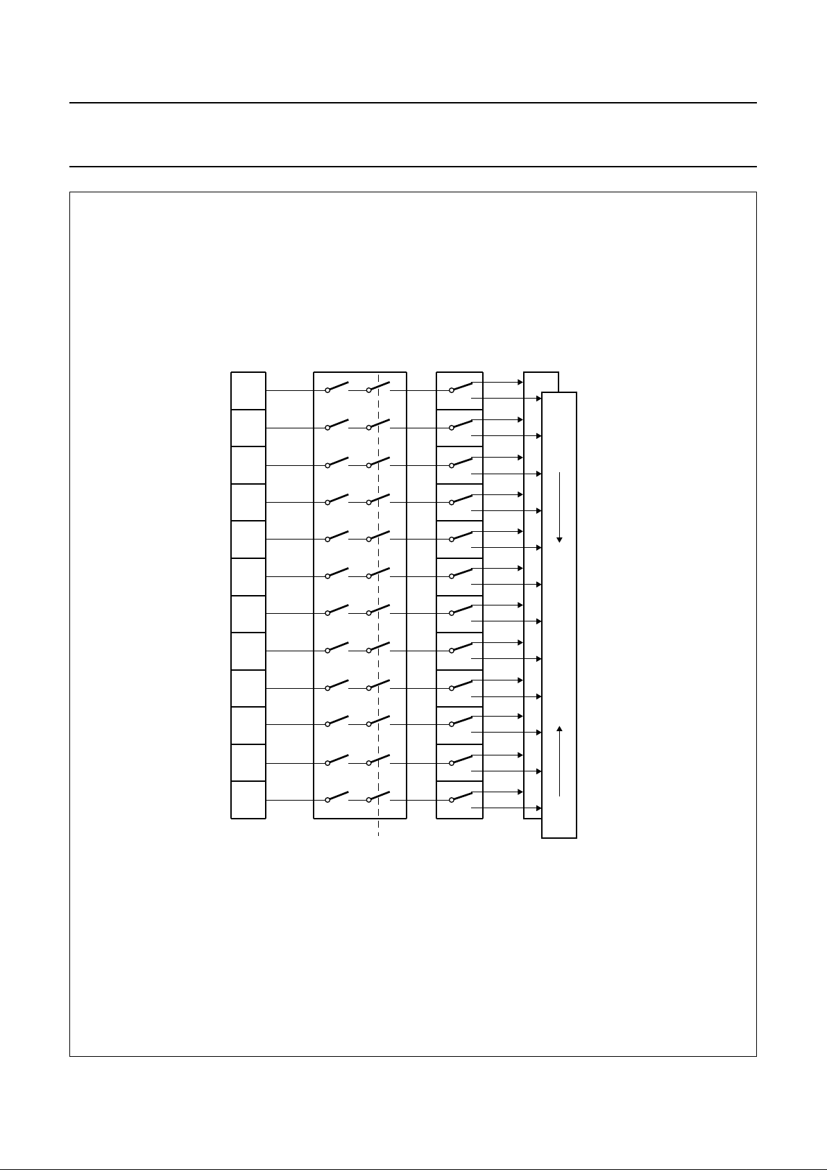
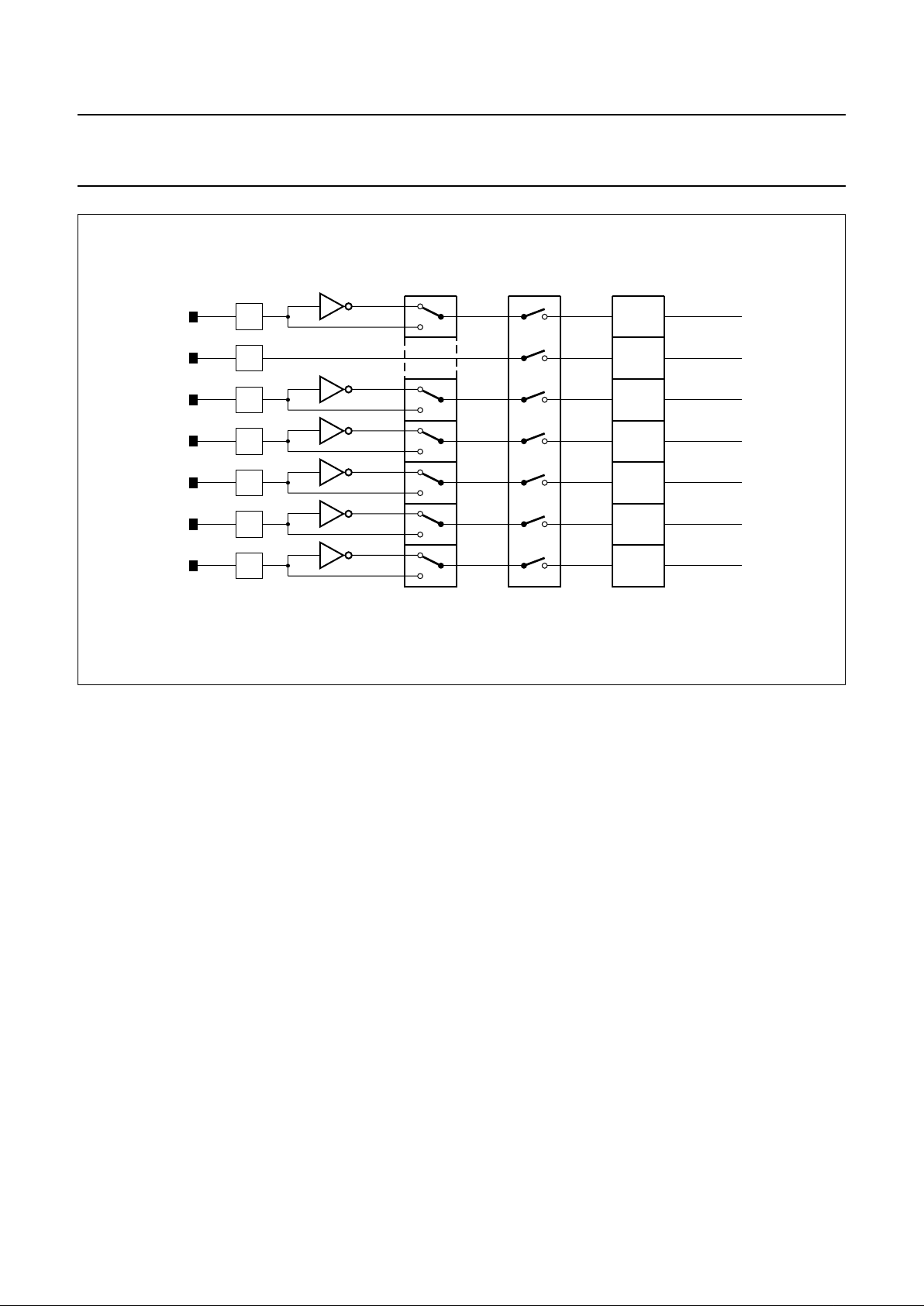
11 INTERRUPT SYSTEM
External events and the real-time driven on-chip
peripherals require service by the CPU asynchronous to
the execution of any particular section of code. To tie the
asynchronous activities of these functions to normal
program execution a multiple-source, two-priority-level,
nested interrupt system is provided. The P8xCx66
acknowledges interrupt requests from twelve sources as
shown in Table 20.
Each interrupt vectors to a separate location in program
memory for its service routine. Each source can be
individually enabled or disabled by using corresponding
bits in the Interrupt Enable Registers (IEN0 and IEN1).
The priority level is selected via the Interrupt Priority
Registers (IP0 and IP1). All enabled sources can be
globally disabled or enabled. The minimum width of the
external interrupt signal is ≥6 XTAL clocks. The maximum
width of the interrupt signal is the total length of all
instructions in the interrupt service routine until the clear
instruction of the IRQ bit. The external interrupts are INT0,
INT1, P1.0, P1.1, P1.2, P1.3, P1.4 and P1.7.
11.1 External interrupts INT2 to INT7 and INT9
Port 1 lines also serve as additional interrupts
INT2 to INT7 (P1.0, P1.1, P1.2, P1.3, P1.4 and P1.7).
INT7 is used by the derivative functional blocks as follows:
X7 VSYNC interrupt 0063H
Using the IX1 register, each pin may be initialized to be
either active HIGH or active LOW except INT7 which is
fixed active HIGH because this interrupt is from another
derivative function. IRQ1 is the Interrupt Request Flag
Register. Each flag will be set on interrupt request but it
must be cleared by software, i.e. via the interrupt software.
11.2 Interrupt priority
Each interrupt source can be set to either high or low
priority. If both priorities are requested simultaneously, the
controller will branch to the high priority vector.
A low priority interrupt can only be interrupted by a high
priority interrupt. A high priority interrupt routine cannot be
interrupted
11.3 Related registers
The following registers are used in conjunction with the
interrupt system.
Table 19 Interrupt registers
REGISTER ADDRESS
Interrupt Polarity Register (IX1) E9H
Interrupt Request Flag Register (IRQ1) C0H
Interrupt Enable Register 0 (IEN0) A8H
Interrupt Enable Register 1 (IEN1);
interrupts INT2 to INT9
E8H
Interrupt Priority Register 0 (IP0) B8H
Interrupt Priority Register 1 (IP1);
interrupts INT2 to INT9
F8H
Table 20 Interrupt request (priority within level)
INTERRUPT MNEMONIC SOURCE VECTOR ADDRESS
PX0 (highest) external interrupt 0 (INT0) 0003H
S1 I2C-bus 002BH
T0 Timer 0 overflow 000BH
PX2 P1.0 port line 0033H
PX6 P1.4 port line 005BH
PX1 external interrupt 1 (INT1) 0013H
PX3 P1.1 port line 003BH
PX7 VSYNC interrupt 0063H
T1 Timer 1 overflow 001BH
PX4 P1.2 port line 0043H
PX5 P1.3 port line 004BH
PX9 (lowest) P1.7 port line 0073H
1999 Mar 10 23
Philips Semiconductors Product specification
Microcontrollers for PAL/SECAM TV
with OSD and VST
P8xCx66 family
Fig.10 Interrupt system.
handbook, full pagewidth
INTERRUPT
SOURCES
PRIORITY
GLOBAL
ENABLE
PX0
S1
T0
PX2
PX6
PX1
PX3
PX7
T1
PX4
PX5
PX9
IEN0/1
REGISTERS
IP0/1
REGISTERS
HIGH
LOW
INTERRUPT POLLING SEQUENCE
MGL297
1999 Mar 10 24
Philips Semiconductors Product specification
Microcontrollers for PAL/SECAM TV
with OSD and VST
P8xCx66 family
Fig.11 External and derivative interrupt configuration.
handbook, full pagewidth
MGL296
P1.7
VSYNC
P1.4
P1.3
P1.2
P1.1
P1.0
X9
X7
X6
X5
X4
X3
X2
IX1
IEN1
IRQ1
1999 Mar 10 25
Philips Semiconductors Product specification
Microcontrollers for PAL/SECAM TV
with OSD and VST
P8xCx66 family
11.4 Interrupt Enable Register 0 (IEN0)
Table 21 Interrupt Enable Register (SFR address A8H)
Table 22 Description of IEN0 bits
A logic 0 disables the interrupt; a logic 1 enables the interrupt.
11.5 Interrupt Enable Register 1 (IEN1)
Table 23 Interrupt Enable Register (SFR address E8H)
Table 24 Description of IEN1 bits
Where EXx = 0, interrupt disabled. EXx = 1, interrupt enabled
76543210
EA − ES1 − ET1 EX1 ET0 EX0
BIT SYMBOL DESCRIPTION
7EAGeneral enable/disable control. When EA = 0, no interrupt is enabled. When EA = 1,
any individually enabled interrupt will be accepted.
6 − not used
5 ES1 enable I
2
C-bus SIO interrupt
4 − not used
3 ET1 enable Timer 1 interrupt
2 EX1 enable external interrupt 1
1 ET0 enable Timer 0 interrupt
0 EX0 enable external interrupt 0
76543210
EX9 − EX7 EX6 EX5 EX4 EX3 EX2
BIT SYMBOL DESCRIPTION
7 EX9 enable external interrupt 9 (P1.7 port line)
6 − not used
5 EX7 enable external interrupt 7 (VSYNC interrupt)
4 EX6 enable external interrupt 6 (P1.4 port line)
3 EX5 enable external interrupt 5 (P1.3 port line)
2 EX4 enable external interrupt 4 (P1.2 port line)
1 EX3 enable external interrupt 3 (P1.1 port line)
0 EX2 enable external interrupt 2 (P1.0 port line)

1999 Mar 10 26
Philips Semiconductors Product specification
Microcontrollers for PAL/SECAM TV
with OSD and VST
P8xCx66 family
11.6 Interrupt Priority Register 0 (IP0)
Table 25 Interrupt Priority Register 0 (SFR address B8H)
Table 26 Description of IP0 bits
A logic 0 selects low priority; a logic 1 selects high priority.
11.7 Interrupt Priority Register 1 (IP1)
Table 27 Interrupt Priority Register 1 (SFR address F8H)
Table 28 Description of IP1 bits
Where PXx = 0 selects low priority; PXx = 1 selects high priority.
76543210
−−PS1 − PT1 PX1 PT0 PX0
BIT SYMBOL DESCRIPTION
7 − These 2 bits are not used.
6 −
5 PS1 I
2
C-bus SIO interrupt priority level
4 − This bit is not used.
3 PT1 Timer 1 interrupt priority level
2 PX1 external interrupt 1 priority level
1 PT0 Timer 0 interrupt priority level
0 PX0 external interrupt 0 priority level
76543210
PX9 − PX7 PX6 PX5 PX4 PX3 PX2
BIT SYMBOL DESCRIPTION
7 PX9 enable external interrupt 9 priority level (P1.7 port line)
6 − not used
5 PX7 enable external interrupt 7 priority level (VSYNC interrupt)
4 PX6 enable external interrupt 6 priority level (P1.4 port line)
3 PX5 enable external interrupt 5 priority level (P1.3 port line)
2 PX4 enable external interrupt 4 priority level (P1.2 port line)
1 PX3 enable external interrupt 3 priority level (P1.1 port line)
0 PX2 enable external interrupt 2 priority level (P1.0 port line)
1999 Mar 10 27
Philips Semiconductors Product specification
Microcontrollers for PAL/SECAM TV
with OSD and VST
P8xCx66 family
11.8 Interrupt Polarity Register (IX1)
Writing a logic 1 to bits IL9, IL6, IL5, IL4, IL3 and IL2 will set the polarity level of the corresponding external interrupt to
be active HIGH. Writing a logic 0 to these bits will set the corresponding external interrupt to be active LOW.
External interrupts INT1 and INT0 however can be programmed to be edge sensitive. Writing a logic 1 to bits IL8 and IL7
will activate the external interrupts INT1 and INT0 on a rising edge (LOW-to-HIGH). Writing a logic 0 to bits IL8 and IL7
will activate the external interrupts INT1 and INT0 on a falling edge (HIGH-to-LOW). This feature is useful for pulse width
measurement; see Section 11.8.1.
Table 29 Interrupt Polarity Register (SFR address E9H)
Table 30 Description of IX1 bits
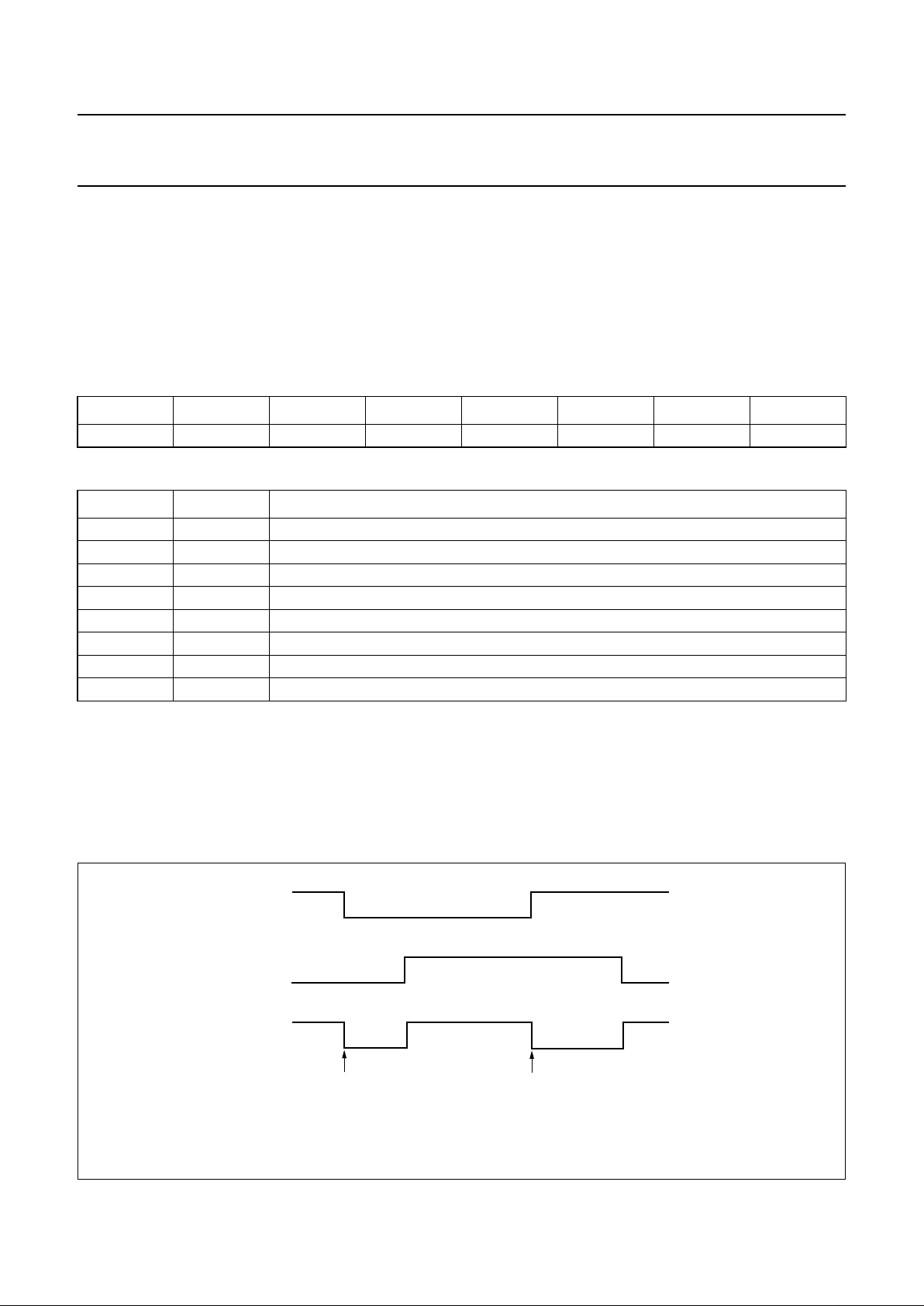
11.8.1 P
ULSE WIDTH MEASUREMENT EXAMPLE
To determine the LOW time of a signal on the external interrupt pin INT0 the following sequence should be followed.
1. External interrupt 0 must be programmed to edge sensitivity (SFR TCON, address 88H).
2. IL7 must be programmed as shown in Fig.12.
3. The value held in Timer 0 or Timer 1 represents the pulse width of the signal on the INT0 pin.
76543210
IL9 IL8 IL7 IL6 IL5 IL4 IL3 IL2
BIT SYMBOL DESCRIPTION
7 IL9 external interrupt 9 polarity level (P1.7 port line)
6 IL8 external interrupt 1 polarity level (INT1) polarity level
5 IL7 external interrupt 0 polarity level (INT0) polarity level
4 IL6 external interrupt 6 polarity level (P1.4 port line)
3 IL5 external interrupt 5 polarity level (P1.3 port line)
2 IL4 external interrupt 4 polarity level (P1.2 port line)
1 IL3 external interrupt 3 polarity level (P1.1 port line)
0 IL2 external interrupt 2 polarity level (P1.0 port line)
Fig.12 Pulse width measurement timing diagram.
handbook, full pagewidth
INT0
IL7
INT0(CPU)
Start interrupt service
routine to start counting
system clock periods
with Timer 0 or Timer 1
Start interrupt service
routine to stop counting
of Timer 0 or Timer 1
MGL295

1999 Mar 10 28
Philips Semiconductors Product specification
Microcontrollers for PAL/SECAM TV
with OSD and VST
P8xCx66 family
11.9 Interrupt Request Flag Register (IRQ1)
Bits IQ9 and IQ6 to IQ2 will be set to a logic 1, if one of the two conditions specified below is met:
• If its associated port line is programmed to generate an interrupt when HIGH (selected using the Interrupt Polarity
Register) and the state of that port line is HIGH
• If its associated port line is programmed to generate an interrupt when LOW (selected using the Interrupt Polarity
Register) and the state of that port line is LOW.
IQ7 is set to a logic 1, if the interrupt condition is met within the corresponding derivative function. Therefore, all IRQ1 bits
serve not only as pending interrupt request bits but also as interrupt status bits. This means that even if the external
interrupts are disabled (using the Interrupt Enable Register 1) the IRQ1 bits can still be set to a logic 1 if the interrupt
condition is met within the corresponding derivative function. For example, if the interrupt condition within VSYNC is met
then:
• If IEN0.7 = X, IEN1.5 = 0 then IRQ1.5 = 1, no pending interrupt to CPU
• If IEN0.7 = 0, IEN1.5 = 1 then IRQ1.5 = 1, interrupt to CPU is pending
• If IEN0.7 = 1, IEN1.5 = 1 then IRQ1.5 = 1, interrupt will be serviced when either:
– The CPU finishes current instruction, if not in the interrupt service routine
– The current interrupt service routine is interrupted if the VSYNC has a higher interrupt priority
– This VSYNC interrupt becomes pending, waiting until the current higher priority level interrupt is serviced.
Bits IQ9 and IQ7 to IQ2 can be reset by software.
Table 31 Interrupt Request Flag Register (SFR address C0H)
Table 32 Description of IRQ1 bits
76543210
IQ9 − IQ7 IQ6 IQ5 IQ4 IQ3 IQ2
BIT SYMBOL DESCRIPTION
7 IQ9 external interrupt 9 request flag (P1.7 port line)
6 − reserved
5 IQ7 external interrupt 7 request flag (VSYNC interrupt)
4 IQ6 external interrupt 6 request flag (P1.4 port line)
3 IQ5 external interrupt 5 request flag (P1.3 port line)
2 IQ4 external interrupt 4 request flag (P1.2 port line)
1 IQ3 external interrupt 3 request flag (P1.1 port line)
0 IQ2 external interrupt 2 request flag (P1.0 port line)
 Loading...