


83C754/87C754
80C51 8-bit microcontroller family
4K/256 OTP/ROM, DAC, comparator, UART, reference
Preliminary specification
Supersedes data of 1997 Dec 03
IC20 Data Handbook
1998 Apr 23
INTEGRATED CIRCUITS

Philips Semiconductors Preliminary specification
83C754/87C754
80C51 8-bit microcontroller family
4K/256 OTP/ROM, DAC, comparator, UART, reference
2
1998 Apr 23
DESCRIPTION
The Philips 83C754/87C754 offers many of the advantages of the
80C51 architecture in a small package and at low cost.
The 8XC754 Microcontroller is fabricated with Philips high-density
CMOS technology. Philips epitaxial substrate minimizes CMOS
latch-up senitivity.
The 8XC754 contains a 4k × 8 ROM (83C754) EPROM (87C754), a
single module PCA, a 256 × 8 RAM, 11 I/O lines, two 16-bit
counter/timers, a two-priority level interrupt structure, a full duplex
serial channel, an on-chip oscillator, and an 8-bit D/A converter.
The EPROM version of this device, the 87C754, is available in
plastic one-time programmable (OTP) packages. Once the array
has been programmed, it ifs functionally equivalent to the masked
ROM 83C754. Thus, unless explicitly stated otherwise, all
references made to the 87C754 apply equally to the 83C754.
The 8XC754 supports two power reduction modes of operation
referred to as the idle mode and the power-down mode.
FEA TURES
•Available in erasable quartz lid or One-Time Programmable plastic
packages
•80C51-based architecture
•Small package sizes – 28-pin SSOP
•Wide oscillator frequency range
•Power control modes:
– Idle mode
– Power-down mode
•4k × 8 ROM (83C754)
EPROM (87C754)
•256 × 8 RAM
•Two 16-bit auto reloadable counter/timers
•Single module PCA counter/timer
•Full duplex serial channel
•Boolean processor
•CMOS and TTL compatible
PIN CONFIGURATION
1
2
3
4
5
6
7
8
9
10
11
12 17
18
19
20
21
22
23
24
25
26
27
28RxD/T0/P3.4/D4
TxD/T1/P3.5/D5
ECI/P3.6/D6
INT1/P3.7/D7
RST
X2
X1
V
SS
ZIN/A2/A10
YIN/A3/A11
XIN/A4
P3.3/D3
P3.2/D2
P3.1/D1
P3.0/D0
INT0/P1.0/A0/A8
CEX/P1.1/A1/A9
V
CC
XYDAC/A7
V
PP
/P1.2
ZDAC/ASEL
XYSOURCE/A6
XYDACBIAS/PGMXYZRAMP/A5
13 16 VREGAV
SS
14 15 DECOUPLEAV
CC
SU00665D
CERAMIC
DUAL
IN-LINE
PACKAGE
AND
PLASTIC
SHRINK
SMALL
OUTLINE
PACKAGE
P ART NUMBER SELECTION
ROM EPROM
1
TEMPERATURE RANGE °C
AND PACKAGE
FREQUENCY
DRAWING
NUMBER
P83C754EBD DB P87C754EBD DB OTP 0 to +70, 28-pin Shrink Small Outline Package 3.5 to 16MHz SOT341-1
NOTE:
1. OTP = One Time Programmable EPROM. UV = UV Erasable EPROM.
Philips Semiconductors Preliminary specification
83C754/87C754
80C51 8-bit microcontroller family
4K/256 OTP/ROM, DAC, comparator, UART, reference
1998 Apr 23
3
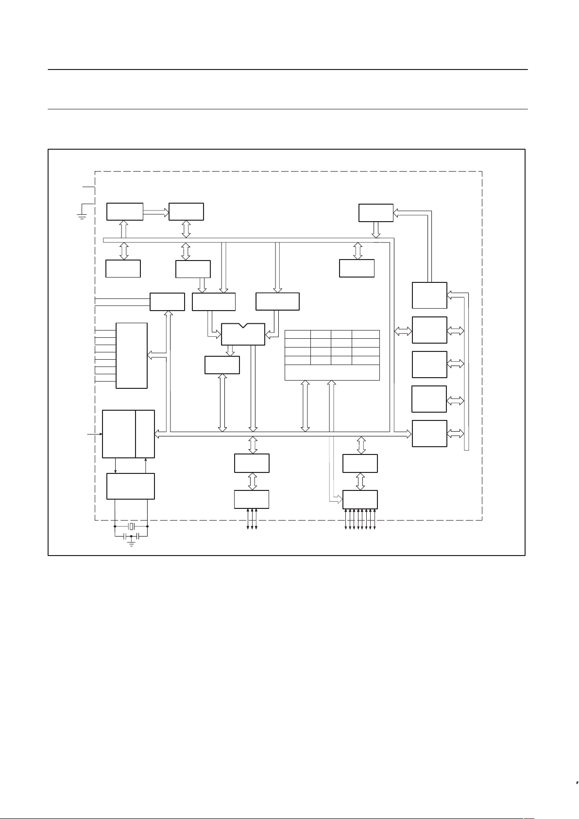
BLOCK DIAGRAM
RST
X1
X2
V
CC
V
SS
RAM
ROM/
EPROM
ACC
TMP2
TMP1
ALU
INSTRUCTION
REGISTER
PD
OSCILLATOR
PSW
BUFFER
DPTR
PCON TCON
IE
TH0 TL0
TH1 TL1
INTERRUPT, SERIAL
PORT AND TIMER BLOCKS
P1.0–P1.2
P3.0–P3.7
DAC
AV
SS
AV
CC
RAM ADDR
REGISTER
STACK
POINTER
PROGRAM
ADDRESS
REGISTER
PC
INCRE-
MENTER
PROGRAM
COUNTER
PORT 3
DRIVERS
PORT 1
DRIVERS
PORT 3
LATCH
PORT 1
LATCH
TIMING
AND
CONTROL
B
REGISTER
SU00666D
ANALOG
X
IN
XYZRAMP
DECOUPLE
VREG
XYDACBIAS
XYSOURCE
ZDAC
XYDAC

Philips Semiconductors Preliminary specification
83C754/87C754
80C51 8-bit microcontroller family
4K/256 OTP/ROM, DAC, comparator, UART, reference
1998 Apr 23
4
PIN DESCRIPTION
MNEMONIC DIP
PIN NO.
TYPE NAME AND FUNCTION
V
SS
8 I Circuit Ground Potential.
V
CC
22 I Supply voltage during normal, idle, and power-down operation.
P1.0–P1.2 21, 23, 24 I/O Port 1: Port 1 is a 3-bit bidirectional I/O port with internal pull-ups on P1.0 and P1.1. Port 1 pins that
have 1s written to them can be used as inputs. As inputs, port 1 pins that are externally pulled low will
source current because of the internal pull-ups (P1.0, P1.1). (See DC Electrical Characteristics: I
IL
).
Port 1 also serves the special function features listed below (Note: P1.0 does not have the strong
pullup that is on for 2 oscillator periods.):
24 I INT0 (P1.0): External interrupt 0.
23 O CEX (P1.1): PCA clock output.
21 I VPP (P1.2): Programming voltage input (open drain).
P3.0–P3.7 1–4,
25–28
I/O Port 3: Port 3 is an 8-bit bidirectional I/O port with internal pull-ups. Port 3 pins that have 1s written to
them are pulled high by the internal pull-ups and can be used as inputs. As inputs, port 3 pins that are
externally being pulled low will source current because of the pull-ups. (See DC Electrical
Characteristics: I
IL
). Port 3 also functions as the data input for the EPROM memory location to be
programmed (or verified). (Note: P3.5 does not have the strong pullup that is on for 2 oscillator
periods.)
Port 3 also serves the special function as listed below:
3 I ECI (P3.6): External PCA clock input.
1 I RxD/T0 (P3.4): Serial port receiver data input.
Timer 0 external clock input.
4 I INT1: External interrupt 1.
2 I TxD/T1 (P3.5): Serial port transmitter data.
Timer 1 external clock input.
RST 5 I Reset: A high on this pin for two machine cycles while the oscillator is running resets the device. After
the device is reset, a 10-bit serial sequence, sent LSB first, applied to RESET, places the device in the
programming state allowing programming address, data and V
PP
to be applied for programming or
verification purposes. The RESET serial sequence must be synchronized with the X1 input. (Note: The
83/87C754 does not have an internal reset resistor.)
X1 7 I Crystal 1: Input to the inverting oscillator amplifier and input to the internal clock generator circuits. X1
also serves as the clock to strobe in a serial bit stream into RESET to place the device in the
programming state.
X2 6 O Crystal 2: Output from the inverting oscillator amplifier .
AV
CC
1
14 I Analog supply voltage and reference input.
AV
SS
1
13 I Analog supply and reference ground.
ZIN 9 I ZIN: Input to analog multiplexer.
YIN 10 I YIN: Input to analog multiplexer.
XIN 11 I XIN: Input to analog multiplexer.
XYZRAMP 12 O XYZRAMP: Provides a low impedance pulldown to VSS under S/W control.
DECOUPLE 15 O Decouple: Output from regulated supply for connection of decoupling capacitors.
VREG 16 O VREG: Provides regulated analog supply output.
XYDACBIAS 17 O XYDACBIAS: Provides source voltage for bias of external circuitry.
– Input which specifies verify mode (output enable) or the program mode.
/PGM = 1 output enabled (verify mode).
/PGM = 0 program mode.
XYSOURCE 18 O XYSOURCE: Provides source voltage from regulated analog supply.
ZDAC 19 O ZDAC: Switchable outp from the internal DAC.
ASEL (P0.0) – Input which indicates which bits of the EPROM address are applied to port 3.
ASEL = 0 low address byte available on port 3.
ASEL = 1 high address byte available on port 3 (only the three least significant bits are used).
XYDAC 20 O XYDAC: Non-switchable output from the internal DAC.
NOTE:
1. AV
SS
(reference ground) must be connected to 0V (ground). AVCC (reference input) cannot differ from VCC by more than ±0.2V, and must be
in the range 4.5V to 5.5V .

Philips Semiconductors Preliminary specification
83C754/87C754
80C51 8-bit microcontroller family
4K/256 OTP/ROM, DAC, comparator, UART, reference
1998 Apr 23
5
OSCILLA T OR CHARACTERISTICS
X1 and X2 are the input and output, respectively, of an inverting
amplifier which can be configured for use as an on-chip oscillator.
To drive the device from an external clock source, X1 should be
driven while X2 is left unconnected. There are no requirements on
the duty cycle of the external clock signal, because the input to the
internal clock circuitry is through a divide-by-two flip-flop. However,
minimum and maximum high and low times specified in the data
sheet must be observed.
IDLE MODE
The 8XC754 includes the 80C51 power-down and idle mode
features. In idle mode, the CPU puts itself to sleep while all of the
on-chip peripherals stay active. The instruction to invoke the idle
mode is the last instruction executed in the normal operating mode
before the idle mode is activated. The CPU contents, the on-chip
RAM, and all of the special function registers remain intact during
this mode. The idle mode can be terminated either by any enabled
interrupt (at which time the process is picked up at the interrupt
service routine and continued), or by a hardware reset which starts
the processor in the same manner as a power-on reset. Upon
powering-up the circuit, or exiting from idle mode, sufficient time
must be allowed for stabilization of the internal analog reference
voltages before a D/A conversion is started.
Special Function Registers
The special function registers (directly addressable only) contain all
of the 8XC754 registers except the program counter and the four
register banks. Most of the special function registers are used to
control the on-chip peripheral hardware. Other registers include
arithmetic registers (ACC, B, PSW), stack pointer (SP) and data
pointer registers (DPH, DPL). Twelve of the SFRs are bit
addressable.
Data Pointer
The data pointer (DPTR) consists of a high byte (DPH) and a low
byte (DPL). In the 80C51 this register allows the access of external
data memory using the MOVX instruction. Since the 83C754 does
not support MOVX or external memory accesses, this register is
generally used as a 16-bit offset pointer of the accumulator in a
MOVC instruction. DPTR may also be manipulated as two
independent 8-bit registers.
POWER-DOWN MODE
In the power-down mode, the oscillator is stopped and the
instruction to invoke power-down is the last instruction executed.
Only the contents of the on-chip RAM are preserved. A hardware
reset is the only way to terminate the power-down mode. The control
bits for the reduced power modes are in the special function register
PCON.
Table 1. External Pin Status During Idle and
Power-Down Modes
MODE Port 1 Port 3
Idle Data Data
Power-down Data Data
ST ANDARD SERIAL INTERFACE
The serial port is full duplex, meaning it can transmit and receive
simultaneously. It is also receive-buffered, meaning it can
commence reception of a second byte before a previously received
byte has been read from the register. (However, if the first byte still
has not been read by the time reception of the second byte is
complete, one of the bytes will be lost.) The serial port receive and
transmit registers are both accessed at Special Function Register
SBUF. Writing to SBUF loads the transmit register, and reading
SBUF accesses a physically separate receive register.
The serial port can operate in 4 modes:
Mode 0: Serial data enters and exits through RxD. TxD outputs the
shift clock. 8 bits are transmitted/received (LSB first). The
baud rate is fixed at 1/12 the oscillator frequency.
Mode 1: 10 bits are transmitted (through TxD) or received (through
RxD): a start bit (0), 8 data bits (LSB first), and a stop bit
(1). On Receive, the stop bit goes into RB8 in Special
Function Register SCON. The baud rate is variable.
Mode 2: 11 bits are transmitted (through TxD) or received (through
RxD): a start bit (0), 8 data bits (LSB first), a
programmable 9th data bit, and a stop bit (1). On Transmit,
the 9th data bit (TB8 in SCON) can be assigned the value
of 0 or 1. Or, for example, the parity bit (P, in the PSW)
could be moved into TB8. On Receive, the 9th data bit
goes into RB8 in Special Function Register SCON, while
the stop bit is ignored. The baud rate is programmable to
either 1/32 or 1/64 the oscillator frequency.
Mode 3: 11 its are transmitted (through TxD) or received (through
RxD): a start bit (0), 8 data bits (LSB first), a
programmable 9th data bit, and a stop bit (1). In fact,
Mode 3 is the same as Mode 2 in all respects except baud
rate. the baud rate in Mode 3 is variable.
In all four modes, transmission is initiated by any instruction that
uses SBUF as a destination register. Reception is initiated in Mode 0
by the condition RI = 0 and REN = 1. Reception is initiated in the
other modes by the incoming start bit if REN = 1.
Multiprocessor Communications
Modes 2 and 2 have a special provision for multiprocessor
communications. In these modes, 9 data bits are received. The 9th
one goes into RB8. Then comes a stop bit. The port can be
programmed such that when the stop bit is received, the serial port
interrupt will be activated only if RB8 = 1. This feature is enabled by
setting bit SM2 in SCON. A way to use this feature in multiprocessor
systems is as follows:
When the master processor wants to transmit a block of data to one
of several slaves, it first sends out an address byte which identifies
the target slave. An address byte differs from a data byte in that the
9th bit is 1 in an address byte and 9 in a data byte. With SM2 = 1,
no slave will be interrupted by a data byte. An address byte,
however, will interrupt all slaves, so that each slave can examine the
received byte and see if it is being addressed. The addressed slave
will clear its SM2 bit and prepare to receive the data bytes that will
be coming. The slaves that were not being addressed leave their
SM2s set, and go on about their business, ignoring the coming data
bytes.
SM2 has no effect in Mode 0, and in Mode 1 can be used to check
the validity of the stop bit. In a Mode 1 reception, if SM2 = 1, the
receive interrupt will not be activated unless a valid stop bit is
received.

Philips Semiconductors Preliminary specification
83C754/87C754
80C51 8-bit microcontroller family
4K/256 OTP/ROM, DAC, comparator, UART, reference
1998 Apr 23
6
Serial Port Control Register
The serial port control and status register is the Special Function
Register SCON, shown in Figure 1. This register contains not only
the mode selection bits, but also the 9th data bit for transmit and
receive (TB8 and RB8), and the serial port interrupt bits (TI and RI).
Baud Rates
The baud rate in Mode 0 is fixed: Mode 0 Baud Rate = Oscillator
Frequency / 12. The baud rate in Mode 2 depends on the value of
bit SMOD in Special function Register PCON. If SMOD = 0 (which is
the value on reset), the baud rate is 1/64 the oscillator frequency.
If SMOD = 1, the baud rate is 1/32 the oscillator frequency.
Mode 2 Baud Rate
2
SMOD
64
(Oscillator Frequency)
In the 8XC754, the baud rates in Modes 1 and 3 are determined by
the Timer 1 overflow rate.
Using Timer 1 to Generate Baud Rates
When Timer 1 is used as the baud rate generator, the baud rates in
Modes 1 and 3 are determined by the Timer 1 overflow rate and the
value of SMOD as follows:
Mode 1, 3 Baud Rate
2
SMOD
32
(Timer 1 Overflow Rate)
The Timer 1 interrupt should be disabled in this application. The
Timer itself can be configured for either “timer” or “counter”
operation, and in any of its 3 running modes. In the most typical
applications, it is configured for “timer” operation, in the auto-reload
mode (high nibble of TMOD = 0010B). In that case the baud rate is
given by the formula:
Mode 1, 3 Baud Rate
2
SMOD
32
Oscillator Frequency
12 [256 (TH1)]
One can achieve very low baud rates with Timer 1 by leaving the
Timer 1 interrupt enabled, and configuring the Timer to run as a
16-bit timer (high nibble of TMOD = 0001B), and using the Timer 1
interrupt to do a 16-bit software reload. Figure 2 lists various
commonly used baud rates and how they can be obtained from
Timer 1.
SM2 Enables the multiprocessor communication feature in Modes 2 and 3. In Mode 2 or 3, if SM2 is set to 1, then Rl will not be
activated if the received 9th data bit (RB8) is 0. In Mode 1, if SM2=1 then RI will not be activated if a valid stop bit was not
received. In Mode 0, SM2 should be 0.
REN Enables serial reception. Set by software to enable reception. Clear by software to disable reception.
TB8 The 9th data bit that will be transmitted in Modes 2 and 3. Set or clear by software as desired.
RB8 In Modes 2 and 3, is the 9th data bit that was received. In Mode 1, it SM2=0, RB8 is the stop bit that was received. In Mode 0,
RB8 is not used.
TI Transmit interrupt flag. Set by hardware at the end of the 8th bit time in Mode 0, or at the beginning of the stop bit in the other
modes, in any serial transmission. Must be cleared by software.
RI Receive interrupt flag. Set by hardware at the end of the 8th bit time in Mode 0, or halfway through the stop bit time in the other
modes, in any serial reception (except see SM2). Must be cleared by software.
MSB
LSB
SM0 SM1 SM2 REN TB8 RB8 TI RI
Where SM0, SM1 specify the serial port mode, as follows:
SM0 SM1 Mode Description Baud Rate
0 0 0 shift register f
OSC
/ 12
0 1 1 8-bit UART variable
1 0 2 9-bit UART f
OSC
/64 or f
OSC
/32
1 1 3 9-bit UART variable
SU00120
Figure 1.
Timer 1
Baud Rate
f
OSC
SMOD
C/T Mode Reload Value
Mode 0 Max: 1.67MHz 20MHz X X X X
Mode 2 Max: 625k 20MHz 1 X X X
Mode 1, 3 Max: 104.2k 20MHz 1 0 2 FFH
19.2k 11.059MHz 1 0 2 FDH
9.6k 11.059MHz 0 0 2 FDH
4.8k 11.059MHz 0 0 2 FAH
2.4k 11.059MHz 0 0 2 F4H
1.2k 11.059MHz 0 0 2 E8H
137.5 11.986MHz 0 0 2 1DH
110 6MHz 0 0 2 72H
110 12MHz 0 0 1 FEEBH
Figure 2. Timer 1 Generated Commonly Used Baud Rates

Philips Semiconductors Preliminary specification
83C754/87C754
80C51 8-bit microcontroller family
4K/256 OTP/ROM, DAC, comparator, UART, reference
1998 Apr 23
7
DIFFERENCES BETWEEN THE 8XC754 AND THE
80C51
Program Memory
On the 8XC754, program memory is 4096 bytes long and is not
externally expandable, so the 80C51 instructions MOVX, LJMP, and
LCALL are not implemented. If these instructions are executed, the
appropriate number of instruction cycles will take place along with
external fetches; however, no operation will take place. The LJMP
may not respond to all program address bits. The only fixed
locations in program memory are the addresses at which execution
is taken up in response to reset and interrupts, which are as follows:
Program Memory
Event Address
Reset 000
External INT0
003
Timer 0 00B
External INT1
013
PCA 01B
SIO/TF1 023
Memory Organization
The 8XC754 manipulates operands in three memory address
spaces. The first is the program memory space which contains
program instructions as well as constants such as look-up tables.
The program memory space contains 4k bytes in the 8XC754.
The second memory space is the data memory array which has a
logical address space of 256 bytes.
The third memory space is the special function register array having
a 128-byte address space (80H to FFH). Only selected locations in
this memory space are used (see Table 2). Note that the
architecture of these memory spaces (internal program memory,
internal data memory , and special function registers) is identical to
the 80C51, and the 8XC754 varies only in the amount of memory
physically implemented.
The 8XC754 does not directly address any external data or program
memory spaces. For this reason, the MOVX instructions in the
80C51 instruction set are not implemented in the 83C754, nor are
the alternate I/O pin functions RD
and WR.
I/O Ports
The I/O pins provided by the 8XC754 consist of port 1 and port 3.
Port 1
Port 1 is a 3-bit bidirectional I/O port and includes alternate functions
on some pins of this port. P1.1 is provided with internal pullups while
the remaining pins (P1.0 and P1.2) are an open drain output
structure. The alternate functions for port 1 are:
INT0 – External interrupt 0.
PCAOUT – PCA clock output
V
PP
– External programming voltage.
Port 3
Port 3 is an 8-bit bidirectional I/O port structure. P3.5 is open drain.
The alternate functions for port 3 are:
RxD – Serial port receiver data input.
T1 – Timer 1 external clock input.
INT1
– External interrupt 1.
TxD – Serial port transmitter data.
T0 – Timer 0 external clock input.
ECI – PCA external clock input.
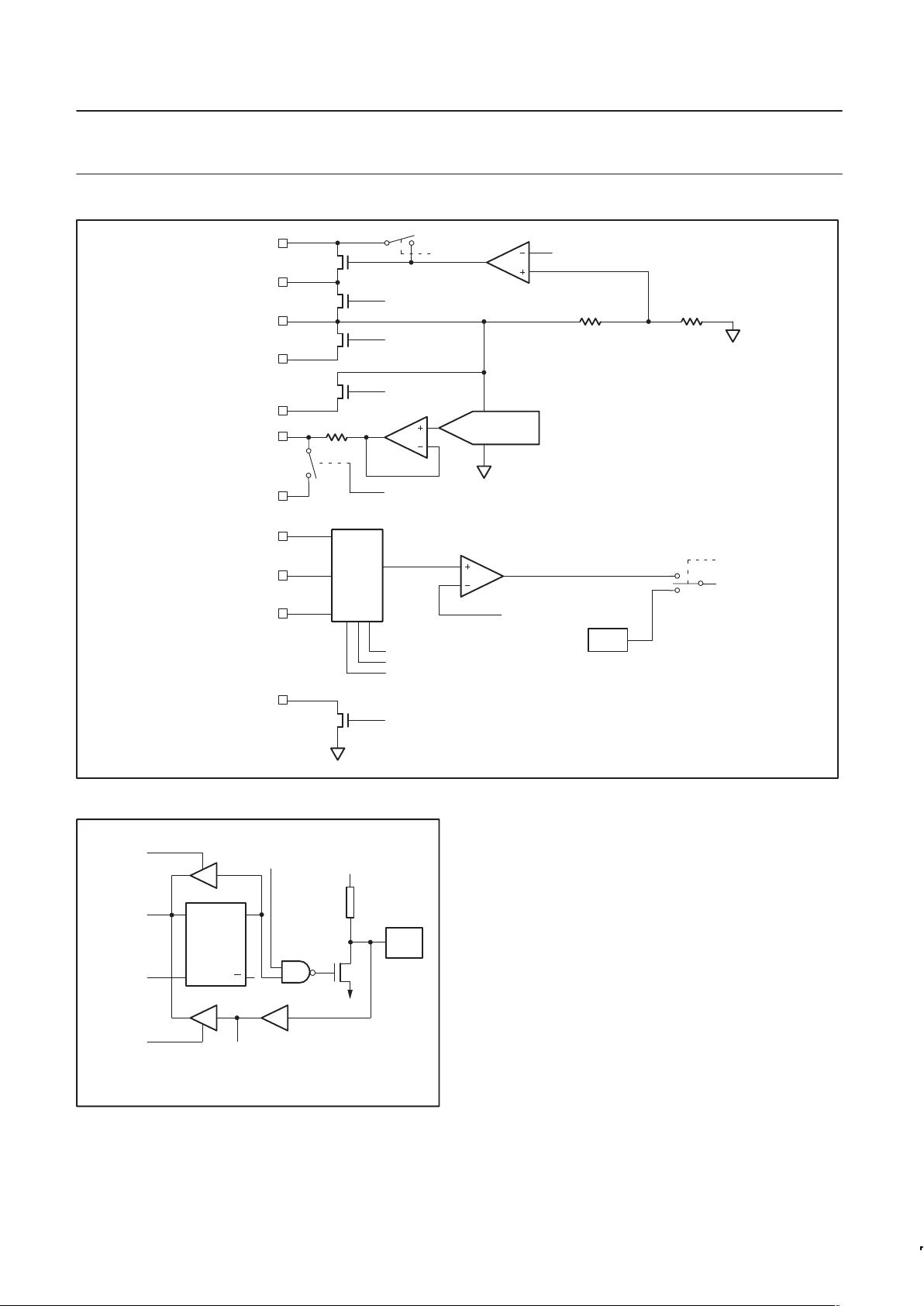
Analog Section
The analog section of the 8XC754, shown in Figure 3, consists of
four major elements: a bandgap referenced voltage regulator, an
8-bit DAC, an input multiplexer and comparator, and a low
impedance pulldown device.
The bandgap voltage regulator uses the AV
CC
pin as its supply and
produces a regulated output on the VREG pin. The bandgap
reference is enabled/disabled by AC0. The regulator also supplies
the analog supply voltage for the DAC. The regulator may be
switched on/off by means of the AC1 bit in the analog control
register (ACON0). The regulator output may also be supplied to the
XYDACBIAS and XYSOURCE pins by means of bits AC3 and AC4,
respectively. The DECOUPLE pin is provided for decoupling the
regulator output.
The DAC is an 8-bit device and its output appears on the XYDAC
pin. In addition, the DAC output may also be routed to the ZDAC pin
by means of bit AC6 in the ACON0 register. The DAC output is not
buffered, so external load impedances should be taken into
consideration when using either of these outputs.
A 3-input multiplexer is provided, whose output is connected to the
positive reference of a comparator. The multiplexer output is
controlled by bits MUX2:0 of ACON1. A bandgap reference supplies
the negative reference of the comparator. The output of the
comparator may be used the trigger the capture input of PCA
module.
A low impedance pulldown is supplied at the XYZRAMP pin and is
controlled by bit AC5 of ACON0.
Interrupt Subsystem—Fixed Priority
The interrupt structure is a seven-source, two-level interrupt system.
Simultaneous interrupt conditions are resolved by a single-level,
fixed priority as follows:
Highest priority:
Pin INT0
Timer flag 0
Lowest priority:
Pin INT1
PCA
Serial I/O – TF1
The vector addresses are as follows:
Source Vector Address
INT0 0003H
TF0 000BH
INT1 0013H
PCA 001BH
SIO/TF1 0023H
Interrupt Enable Register
MSB LSB
EA
– – ES/T1 EC EX1 ET0 EX0
Position Symbol Function
IE.7 EA Global interrupt disable when EA = 0
IE.6 –
IE.5 –
IE.4 ES/T1 Serial port/Timer Flag 1
IE.3 EC PCA interrupt
IE.2 EX1 External interrupt 1
IE.1 ET0 Timer 0 overflow
IE.0 EX0 External interrupt 0
Philips Semiconductors Preliminary specification
83C754/87C754
80C51 8-bit microcontroller family
4K/256 OTP/ROM, DAC, comparator, UART, reference
1998 Apr 23
8
AV
CC
DECOUPLE
VREG
BANDGAP REF*
AC2
XYDACBIAS
20K 10K
XYSOURCE
XYDAC
AC4
AC3
ZDAC
1K
AC6
ANALOG
MUX
ZIN
YIN
XIN
MUX0
MUX1
TO PCA TRIGGER
BANDGAP REF
XYZRAMP
AC5
SU00765A
AC1
*ENABLED/DISABLED BY AC0
EXT
AC7
MUX2
DCON 7:0 (84H)
Figure 3. Analog Section
LATCH
DQ
CL Q
READ
LATCH
INT. BUS
WRITE TO
LATCH
READ
PIN
ALTERNATE INPUT
FUNCTION
V
DD
PIN
INTERNAL*
PULL-UP
ALTERNATE
OUTPUT
FUNCTION
SU00671
*PINS LISTED AS OPEN DRAIN WILL NOT HAVE THIS PULLUP
Figure 4. Typical Port Bit Latches and I/O Buffers
 Loading...