

Philips P83C749EBPN, P83C749EBDDB, P83C749EBAA Datasheet

INTEGRATED CIRCUITS
83C749/87C749
80C51 8-bit microcontroller family
2K/64 OTP/ROM, 5 channel 8-bit A/D, PWM,
low pin count
Preliminary specification
Supersedes data of 1998 Jan 06
IC20 Data Handbook
1998 Apr 23
Philips Semiconductors Preliminary specification
80C51 8-bit microcontroller family
2K/64 OTP/ROM, 5 channel 8-bit A/D, PWM, low pin count
DESCRIPTION
The Philips 83C749/87C749 offers many of the advantages of the
80C51 architecture in a small package and at low cost.
The 8XC749 Microcontroller is fabricated with Philips high-density
CMOS technology. Philips epitaxial substrate minimizes CMOS
latch-up sensitivity.
The 8XC749 contains a 2k × 8 ROM (83C749) EPROM (87C749), a
64 × 8 RAM, 21 I/O lines, a 16-bit auto-reload counter/timer, a
fixed-priority level interrupt structure, an on-chip oscillator, a five
channel multiplexed 8-bit A/D converter, and an 8-bit PWM output.
The EPROM version of this device, the 87C749, is available in
plastic one-time programmable (OTP) packages. Once the array
has been programmed, it is functionally equivalent to the masked
ROM 83C749. Thus, unless explicitly stated otherwise, all
references made to the 83C749 apply equally to the 87C749.
The 83C749 supports two power reduction modes of operation
referred to as the idle mode and the power-down mode.
FEA TURES
•Available in erasable quartz lid or One-Time Programmable plastic
packages
•80C51 based architecture
•Small package sizes
– 28-pin DIP
– 28-pin Shrink Small Outline Package (SSOP)
– 28-pin PLCC
•Wide oscillator frequency range: 3.5MHz to 16MHz
•Low power consumption:
– Normal operation: less than 11mA @ 5V, 12MHz
– Idle mode
– Power-down mode
•2k × 8 ROM (83C749)
EPROM (87C749)
•64 × 8 RAM
•16-bit auto reloadable counter/timer
•5-channel 8-bit A/D converter
•8-bit PWM output/timer
•10-bit fixed-rate timer
•Boolean processor
•CMOS and TTL compatible
•Well suited for logic replacement, consumer and industrial
applications
83C749/87C749
P ART NUMBER SELECTION
ROM EPROM
P83C749EBP N P87C749EBP N OTP 0 to +70, 28-pin Plastic Dual In-line Package 3.5 to 16MHz SOT117-2
P83C749EBA A P87C749EBA A OTP 0 to +70, 28-pin Plastic Leaded Chip Carrier 3.5 to 16MHz SOT261-3
P83C749EBD DB P87C749EBD DB OTP 0 to +70, 28-pin Shrink Small Outline Package 3.5 to 16MHz SOT341-1
NOTE:
1. OTP = One Time Programmable EPROM.
1
TEMPERATURE RANGE °C
AND PACKAGE
FREQUENCY
DRAWING
NUMBER
1998 Apr 23
2

Philips Semiconductors Preliminary specification
80C51 8-bit microcontroller family
2K/64 OTP/ROM, 5 channel 8-bit A/D, PWM, low pin count
BLOCK DIAGRAM
P0.0–P0.4
PORT 0
DRIVERS
V
CC
V
SS
RAM ADDR
REGISTER
B
REGISTER
RAM
ACC
TMP2
PSW
PORT 0
LATCH
ALU
PWM
PORT 2
LATCH
TMP1
PCON TCON
TH0 TL0
RTH RTL
INTERRUPT AND
TIMER BLOCKS
STACK
POINTER
IE
ROM/
EPROM
83C749/87C749
PROGRAM
ADDRESS
REGISTER
BUFFER
PC
INCRE-
MENTER
RST
TIMING
AND
CONTROL
OSCILLATOR
X1
INSTRUCTION
PD
REGISTER
X2
AV
ADC
SSAVCC
PORT 1
LATCH
PORT 1
DRIVERS
P1.0–P1.7
PORT 3
LATCH
PORT 3
DRIVERS
P3.0–P3.7
PROGRAM
COUNTER
DPTR
SU00305
1998 Apr 23
3

Philips Semiconductors Preliminary specification
80C51 8-bit microcontroller family
2K/64 OTP/ROM, 5 channel 8-bit A/D, PWM, low pin count
PIN CONFIGURATION
P3.4/A4
P3.3/A3
P3.2/A2/A10
P3.1/A1/A9
P3.0/A0/A8
P0.2/V
P0.1/OE–PGM
P0.0/ASEL
RST
V
P1.0/ADC0/D0
P1.1/ADC1/D1
1
2
3
4
5
PLASTIC
DUAL
6
PP
X2
X1
SS
7
8
9
10
11
12
13
14
IN-LINE
PACKAGE
AND
SHRINK
SMALL
OUTLINE
PACKAGE
V
28
CC
P3.5/A5
27
P3.6/A6
26
P3.7/A7
25
24
P0.4/PWM OUT
23
P0.3
22
P1.7/T0/D7
21
P1.6/INT1/D6
20
P1.5/INT0/D5
19
AV
CC
18
AV
SS
17
P1.4/ADC4/D4
16
P1.3/ADC3/D3
15
P1.2/ADC2/D2
83C749/87C749
4126
5
11
12 18
Pin Function
1 P3.4/A4
2 P3.3/A3
3 P3.2/A2/A10
4 P3.1/A1/A9
5 P3.0/A0/A8
6 P0.2/V
7 P0.1/OE-PGM
8 P0.0/ASEL
9 RST
10 X2
11 X1
12 V
13 P1.0/ADC0/D0
14 P1.1/ADC1/D1
PP
SS
PLASTIC
LEADED
CHIP
CARRIER
Pin Function
15 P1.2/ADC2/D2
16 P1.3/ADC3/D3
17 P1.4/ADC4/D4
18 AV
19 AV
20 P1.5/INT0/D5
21 P1.6/INT1
22 P1.7/T0/D7
23 P0.3
24 P0.4/PWM OUT
25 P3.7/A7
26 P3.6/A6
27 P3.5/A5
28 V
25
19
SS
CC
/D6
CC
SU00304
1998 Apr 23
4

Philips Semiconductors Preliminary specification
80C51 8-bit microcontroller family
83C749/87C749
2K/64 OTP/ROM, 5 channel 8-bit A/D, PWM, low pin count
PIN DESCRIPTION
MNEMONIC PIN NO. TYPE NAME AND FUNCTION
V
SS
V
CC
P0.0–P0.4 8–6
P1.0–P1.7 13–17,
P3.0–P3.7 5–1,
RST 9 I Reset: A high on this pin for two machine cycles while the oscillator is running resets the device. An
X1 11 I Crystal 1: Input to the inverting oscillator amplifier and input to the internal clock generator circuits. X1
X2 10 O Crystal 2: Output from the inverting oscillator amplifier.
1
AV
CC
1
AV
SS
NOTE:
1. AV
(reference ground) must be connected to 0V (ground). AVCC (reference input) cannot differ from VCC by more than ±0.2V, and must be
SS
in the range 4.5V to 5.5V .
2. When P0.2 is at or close to 0 volt, it may affect the internal ROM operation. We recommend that P0.2 be tied to V
(e.g., 2kΩ).
12 I Circuit Ground Potential.
28 I Supply voltage during normal, idle, and power-down operation.
I/O Port 0: Port 0 is a 5-bit bidirectional port. Port 0.0–P0.2 are open drain. Port 0.0–P0.2 pins that have
23, 24
1s written to them float, and in that state can be used as high-impedance inputs. P0.3–P0.4 are
bidirectional I/O port pins with internal pull-ups. These pins are driven low if the port register bit is
written with a 0. The state of the pin can always be read from the port register by the program. Port 0.3
and 0.4 have internal pull-ups that function identically to port 3. Pins that have 1s written to them are
pulled high by the internal pull-ups and can be used as inputs.
While P0.0 anbd P0.1 differ from “standard TTL” characteristics, they are close enough for the pins to
still be used as general-purpose I/O.
6 I VPP (P0.2) – Programming voltage input. (See Note 2.)
7 I OE/PGM (P0.1) – Input which specifies verify mode (output enable) or the program mode.
OE/PGM = 1 output enabled (verify mode).
OE/PGM = 0 program mode.
8 I ASEL (P0.0) – Input which indicates which bits of the EPROM address are applied to port 3.
ASEL = 0 low address byte available on port 3.
ASEL = 1 high address byte available on port 3 (only the three least significant bits are used).
I/O Port 1: Port 1 is an 8-bit bidirectional I/O port with internal pull-ups. Port 1 pins that have 1s written to
20–22
them are pulled high by the internal pull-ups and can be used as inputs. P0.3–P0.4 pins are
bidirectional I/O port pins with internal pull-ups. As inputs, port 1 pins that are externally pulled low will
source current because of the internal pull-ups. (See DC Electrical Characteristics: I
serves the special function features of the SC80C51 family as listed below:
). Port 1 also
IL
20 I INT0 (P1.5): External interrupt.
21 I INT1 (P1.6): External interrupt.
22 I T0 (P1.7): T imer 0 external input.
13–17 I ADC0 (P1.0)–ADC4 (P1.4): Port 1 also functions as the inputs to the five channel multiplexed A/D
converter. These pins can be used as outputs only if the A/D function has been disabled. These pins
can be used as digital inputs while the A/D converter is enabled.
Port 1 serves to output the addressed EPROM contents in the verify mode and accepts as inputs the
value to program into the selected address during the program mode.
I/O Port 3: Port 3 is an 8-bit bidirectional I/O port with internal pull-ups. Port 3 pins that have 1s written to
27–25
them are pulled high by the internal pull-ups and can be used as inputs. As inputs, port 3 pins that are
externally being pulled low will source current because of the pull-ups. (See DC Electrical
Characteristics: I
programmed (or verified). The 11-bit address is multiplexed into this port as specified by P0.0/ASEL.
). Port 3 also functions as the address input for the EPROM memory location to be
IL
internal diffused resistor to VSS permits a power-on RESET using only an external capacitor to VCC.
After the device is reset, a 10-bit serial sequence, sent LSB first, applied to RESET, places the device
in the programming state allowing programming address, data and V
or verification purposes. The RESET serial sequence must be synchronized with the X1 input.
to be applied for programming
PP
also serves as the clock to strobe in a serial bit stream into RESET to place the device in the
programming state.
19 I Analog supply voltage and reference input.
18 I Analog supply and reference ground.
via a small pullup
CC
1998 Apr 23
5

Philips Semiconductors Preliminary specification
80C51 8-bit microcontroller family
2K/64 OTP/ROM, 5 channel 8-bit A/D, PWM, low pin count
OSCILLA T OR CHARACTERISTICS
X1 and X2 are the input and output, respectively, of an inverting
amplifier which can be configured for use as an on-chip oscillator.
To drive the device from an external clock source, X1 should be
driven while X2 is left unconnected. There are no requirements on
the duty cycle of the external clock signal, because the input to the
internal clock circuitry is through a divide-by-two flip-flop. However,
minimum and maximum high and low times specified in the data
sheet must be observed.
IDLE MODE
The 8XC749 includes the 80C51 power-down and idle mode
features. In idle mode, the CPU puts itself to sleep while all of the
on-chip peripherals except the A/D and PWM stay active. The
functions that continue to run while in the idle mode are Timer 0,
Timer I, and the interrupts. The instruction to invoke the idle mode is
the last instruction executed in the normal operating mode before
the idle mode is activated. The CPU contents, the on-chip RAM, and
all of the special function registers remain intact during this mode.
The idle mode can be terminated either by any enabled interrupt (at
which time the process is picked up at the interrupt service routine
and continued), or by a hardware reset which starts the processor in
the same manner as a power-on reset. Upon powering-up the
circuit, or exiting from idle mode, sufficient time must be allowed for
stabilization of the internal analog reference voltages before an A/D
conversion is started.
Special Function Registers
The special function registers (directly addressable only) contain all
of the 8XC751 registers except the program counter and the four
register banks. Most of the 21 special function registers are used to
control the on-chip peripheral hardware. Other registers include
arithmetic registers (ACC, B, PSW), stack pointer (SP) and data
pointer registers (DPH, DPL). Nine of the SFRs are bit addressable.
Data Pointer
The data pointer (DPTR) consists of a high byte (DPH) and a low
byte (DPL). In the 80C51 this register allows the access of external
data memory using the MOVX instruction. Since the 83C749 does
not support MOVX or external memory accesses, this register is
generally used as a 16-bit offset pointer of the accumulator in a
MOVC instruction. DPTR may also be manipulated as two
independent 8-bit registers.
POWER-DOWN MODE
In the power-down mode, the oscillator is stopped and the
instruction to invoke power-down is the last instruction executed.
Only the contents of the on-chip RAM are preserved. A hardware
reset is the only way to terminate the power-down mode. The control
bits for the reduced power modes are in the special function register
PCON.
Table 1. External Pin Status During Idle and
Power-Down Modes
MODE Port 0* Port 1 Port 2
Idle Data Data Data
Power-down Data Data Data
* Except for PWM output (P0.4).
DIFFERENCES BETWEEN THE 8XC749 AND THE 80C51
Program Memory
On the 8XC749, program memory is 2048 bytes long and is not
externally expandable, so the 80C51 instructions MOVX, LJMP, and
LCALL are not implemented. If these instructions are executed, the
appropriate number of instruction cycles will take place along with
external fetches; however, no operation will take place. The LJMP
may not respond to all program address bits. The only fixed
locations in program memory are the addresses at which execution
is taken up in response to reset and interrupts, which are as follows:
Event Address
Reset 000
External INT0
Counter/timer 0 00B
External INT1 013
Timer I 01B
ADC 02B
PWM 033
Memory Organization
The 8XC749 manipulates operands in three memory address
spaces. The first is the program memory space which contains
program instructions as well as constants such as look-up tables.
The program memory space contains 2k bytes in the 8XC749.
The second memory space is the data memory array which has a
logical address space of 128 bytes. However, only the first 64 (0 to
3FH) are implemented in the 8XC749.
The third memory space is the special function register array having
a 128-byte address space (80H to FFH). Only selected locations in
this memory space are used (see Table 2). Note that the
architecture of these memory spaces (internal program memory,
internal data memory , and special function registers) is identical to
the 80C51, and the 8XC749 varies only in the amount of memory
physically implemented.
The 8XC749 does not directly address any external data or program
memory spaces. For this reason, the MOVX instructions in the
80C51 instruction set are not implemented in the 83C749, nor are
the alternate I/O pin functions RD
I/O Ports
The I/O pins provided by the 83C749 consist of port 0, port 1, and
port 3.
Port 0
Port 0 is a 5-bit bidirectional I/O port and includes alternate functions
on some pins of this port. Pins P0.3 and P0.4 are provided with
internal pullups while the remaining pins (P0.0, P0.1, and P0.2) have
open drain output structures. The alternate function for port P0.4 is
PWM output.
If the alternate function PWM is not being used, then this pin may be
used as an I/O port.
83C749/87C749
Program Memory
003
and WR.
1998 Apr 23
6
Philips Semiconductors Preliminary specification
80C51 8-bit microcontroller family
2K/64 OTP/ROM, 5 channel 8-bit A/D, PWM, low pin count
Port 1
Port 1 is an 8-bit bidirectional I/O port whose structure is identical to
the 80C51, but also includes alternate input functions on all pins.
The alternate pin functions for port 1 are:
P1.0-P1.4 - ADC0-ADC4 - A/D converter analog inputs
P1.5 INT0
P1.6 INT1
- external interrupt 0 input
- external interrupt 1 input
P1.7 - T0 - timer 0 external input
If the alternate functions INT0
, INT1, or T0 are not being used, these
pins may be used as standard I/O ports. It is necessary to connect
and AVSS to VCC and VSS, respectively, in order to use P1.5,
AV
CC
P1.6, and P1.7 pins as standard I/O pins. When the A/D converter is
enabled, the analog channel connected to the A/D may not be used
as a digital input; however, the remaining analog inputs may be used
as digital inputs. They may not be used as digital outputs. While the
A/D is enabled, the analog inputs are floating.
Port 3
Port 3 is an 8-bit bidirectional I/O port whose structure is identical to
the 80C51. Note that the alternate functions associated with port 3
of the 80C51 have been moved to port 1 of the 83C749 (as
applicable). See Figure 1 for port bit configurations.
Counter/Timer Subsystem
The 8XC749 has one counter/timer called timer/counter 0. Its
operation is similar to mode 2 operation on the 80C51, but is
extended to 16 bits with 16 bits of autoload. The controls for this
counter are centralized in a single register called TCON.
Timer I Implementation
Timer I is clocked once per machine cycle, which is the oscillator
frequency divided by 12. The timer operation is enabled by setting
the TIRUN bit (bit 4) in the I2CFG register. Writing a 0 into the
TIRUN bit will stop and clear the timer. The timer is 10 bits wide, and
when it reaches the terminal count of 1024, it carries out and sets
the Timer I interrupt flag. An interrupt will occur if the Timer I
interrupt is enabled by bit ETI (bit 4) of the Interrupt Enable (IE)
register, and global interrupts are enabled by bit EA (bit 7) of the
same IE register.
The vector address for the Timer I interrupt is 1Bhex, and the
interrupt service routine must start at this address. As with all 8051
family microcontrollers, only the Program Counter is pushed onto
the stack upon interrupt (other registers that are used both by the
interrupt service routine and elsewhere must be explicitly saved).
The Timer I interrupt flag is cleared by setting the CKRTI bit (bit 5 of
the I1CFG register. For more information, see application note
AN427.
Interrupt Subsystem—Fixed Priority
The IP register and the 2-level interrupt system of the 80C51 are
eliminated. The interrupt structure is a seven-source, one-level
interrupt system similar to the 8XC751. Simultaneous interrupt
conditions are resolved by a single-level, fixed priority as follows:
Highest priority: Pin INT0
Lowest priority: ADC
The vector addresses are as follows:
Source Vector Address
INT0 0003H
TF0 000BH
INT1 0013H
TIMER I 001BH
ADC 002BH
PWM 0033H
Interrupt Control Registers
The 80C51 interrupt enable register is modified to take into account
the different interrupt sources of the 8XC749.
Interrupt Enable Register
MSB LSB
EA
Position Symbol Function
IE.7 EA Global interrupt disable when EA = 0
IE.6 EAD A/D conversion complete
IE.5 ETI Timer I
IE.4 —
IE.3 EPWM PWM counter overflow
IE.2 EX1 External interrupt 1
IE.1 ET0 Timer 0 overflow
IE.0 EX0 External interrupt 0
83C749/87C749
Counter/timer flag 0
Pin INT1
PWM
Timer I
EAD ETI — EPWM EX1 ET0 EX0
READ
LATCH
INT. BUS
WRITE TO
LATCH
READ
1998 Apr 23
PIN
ALTERNATE
OUTPUT
FUNCTION
DQ
P1.X
LATCH
CL Q
ALTERNATE INPUT
FUNCTION
READ
V
DD
INTERNAL
PULL-UP
P1.X
PIN
LATCH
INT. BUS
WRITE TO
LATCH
READ
PIN
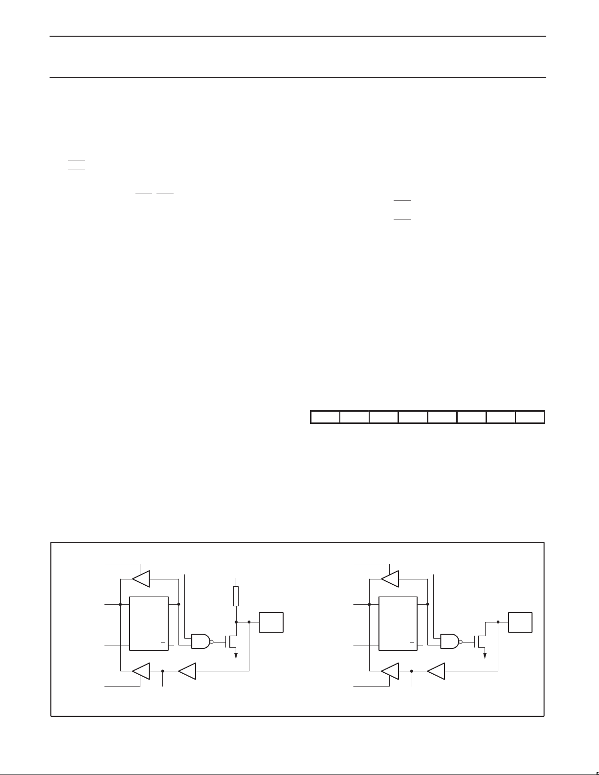
Figure 1. Port Bit Latches and I/O Buffers
7
ALTERNATE
OUTPUT
FUNCTION
DQ
P0.X
LATCH
CL Q
ALTERNATE INPUT
FUNCTION
P0.X
PIN
SU00306
 Loading...