

Philips P87C591, P83C591, P80C591 Datasheet

DATA SH EET
Objective Specification
File under Integrated Circuits, IC20
1999 Aug 19
INTEGRATED CIRCUITS
P8xC591
Single-chip 8-bit microcontroller
with CAN controller

1999 Aug 19 2
Philips Semiconductors Objective Specification
Single-chip 8-bit microcontroller with CAN controller P8xC591
CONTENTS
1 FEATURES
1.1 80C51 Related Features of the 8xC591
1.2 CAN Related Features of the 8xC591
2 GENERAL DESCRIPTION
3 ORDERING INFORMATION
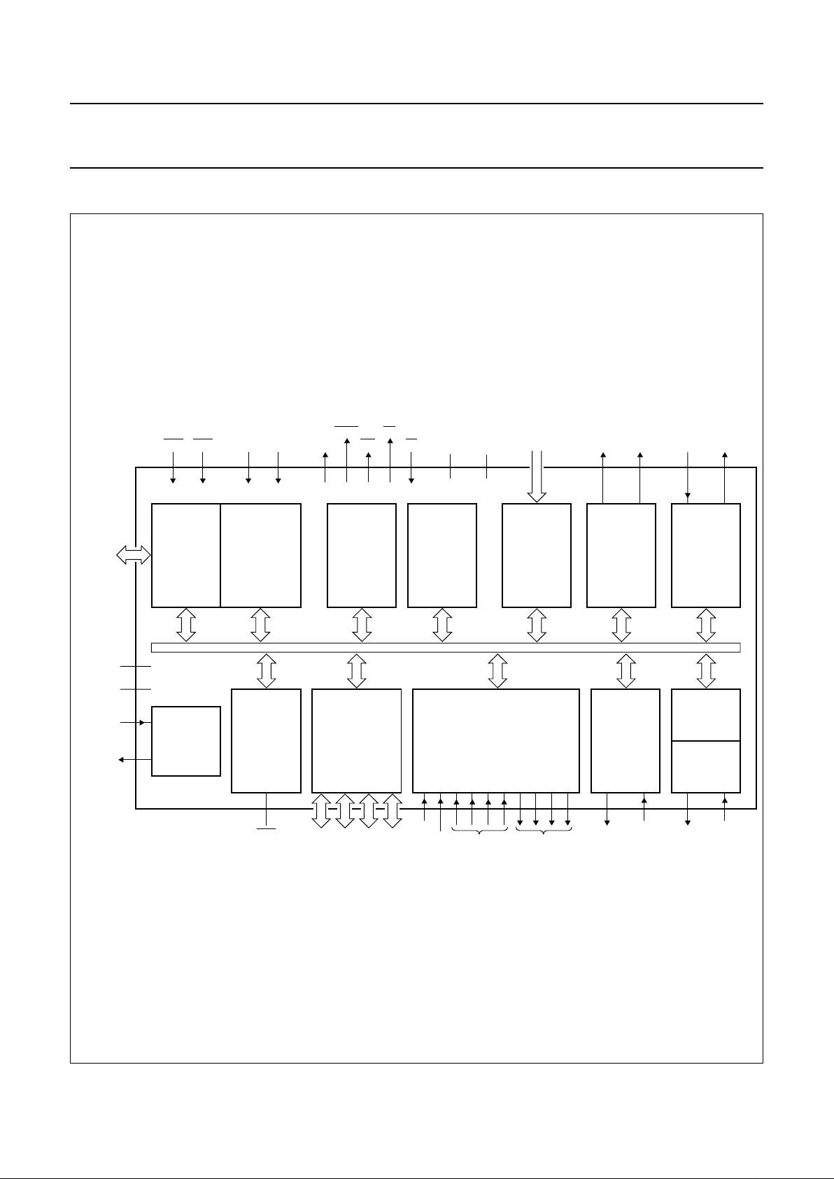
4 BLOCK DIAGRAM
5 FUNCTIONAL DIAGRAM
6 PINNING INFORMATION
6.1 Pinning diagram
6.2 Pin description
7 MEMORY ORGANIZATION
7.1 Program Memory
7.2 Addressing
7.3 Expanded Data RAM addressing
7.4 Dual DPTR
8 I/O FACILITIES
9 OSCILLATOR CHARACTERISTICS
10 RESET
11 LOW POWER MODES
11.1 Stop Clock Mode
11.2 Idle Mode
11.3 Power-down Mode
12 CAN, CONTROLLER AREA NETWORK
12.1 Features of the PeliCAN Controller
12.2 PeliCAN structure
12.3 Communication between PeliCAN Controller
and CPU
12.4 Register and Message Buffer description
12.5 CAN Registers
13 SERIAL I/O
14 SIO0 STANDARD SERIAL INTERFACE UART
14.1 Multiprocessor Communications
14.2 Serial Port Control Register
14.3 Baud Rate Generation
14.4 More about UART Modes
14.5 Enhanced UART
15 SIO1, I2C SERIAL IO
15.1 Modes of Operation
15.2 SIO1 Implementation and Operation
15.3 Software Examples of SIO1 Service Routines
16 TIMER 2
16.1 Features of Timer 2
17 WATCHDOG TIMER (T3)
18 PULSE WIDTH MODULATED OUTPUTS
18.1 Prescaler Frequency Control Register (PWMP)
18.2 Pulse Width Register 0 (PWM0)
18.3 Pulse Width Register 1 (PWM1)
19 PORT 1 OPERATION
20 ANALOG-TO-DIGITAL CONVERTER (ADC)
20.1 ADC features
20.2 ADC functional description
20.3 10-Bit Analog-to-Digital Conversion
20.4 10-Bit ADC Resolution and Analog Supply
20.5 Power Reduction Modes
21 INTERRUPTS
21.1 Interrupt Enable Registers
21.2 Interrupt Enable and Priority Registers
21.3 Interrupt priority
21.4 Interrupt Vectors
22 INSTRUCTION SET
22.1 Addressing Modes
23 LIMITING VALUES
24 DC CHARACTERISTICS (VALUES IN THIS
TABLE NOT CONFIRMED)
25 AC CHARACTERISTICS
25.1 Timing symbol definitions
26 EPROM CHARACTERISTICS
26.1 Program verification
26.2 Security bits
27 PACKAGE OUTLINES
28 SOLDERING
28.1 Plastic leaded-chip carriers/quad flat-packs
29 DEFINITIONS
30 LIFE SUPPORT APPLICATIONS

1999 Aug 19 3
Philips Semiconductors Objective Specification
Single-chip 8-bit microcontroller with CAN controller P8xC591
1 FEATURES
1.1 80C51 Related Features of the 8xC591
• Full static 80C51 Central Processing Unit available as
OTP, ROM and ROMless
• 16 Kbytes internal Program Memory expandable
externally to 64 Kbytes
• 512 bytes on-chip Data RAM expandable externally to
64 Kbytes
• Three 16-bit timers/counters T0, T1 (standard 80C51)
and additional T2 (capture & compare)
• 10-bit ADC with 6 multiplexed analog inputs with fast
8-bit ADC option
• Two 8-bit resolution, Pulse Width Modulated outputs
• 32 I/O port pins in the standard 80C51 pinout
• I2C-bus serial I/O port with byte oriented master and
slave functions
• On-chip Watchdog Timer T3
• Extended temperature range: −40 to +85°C
• Accelerated (prescaler 1:1) instruction cycle time
375 ns @ 16 MHz
• Operation voltage range: 5 V ± 10%
• Security bits:
– ROM version has 2 bits
– OTP/EPROM version has 3 bits
• 64 bytes Encryption array
• 4 level priority interrupt, 15 interrupt sources
• Full-duplex enhanced UART with programmable
Baudrate Generator
• Power Control Modes:
– Clock can be stopped and resumed
– Idle Mode
– Power-down Mode
• ADC active in Idle Mode
• Second DPTR register
• ALE inhibit for EMI reduction
• Programmable I/O port pins (pseudo bi-directional,
push-pull, high impedance, open drain)
• Wake-up from Power-down by external interrupts
• Software reset bit (AUXR1.5)
• Low active reset pin
• Power-on detect reset
• Once mode
1.2 CAN Related Features of the 8xC591
• CAN 2.0B active controller, supporting 11-bit Standard
and 29-bit Extended indentifiers
• 1 Mbit/s CAN bus speed with 8 MHz clock achievable
• 64 byte receive FIFO (can capture sequential Data
Frames from the
same
source as required by the
Transport Layer of higher protocols such as DeviceNet,
CANopen and OSEK)
• 13 byte transmit buffer
• Enhanced PeliCAN core (from the SJA1000 stand-alone
CAN2.0B controller)
1.2.1 PELICAN FEATURES
• Four independently configurable Screeners
(Acceptance Filters)
• Each Screener has tow 32-bit specifiers:
– 32-bit Match and
– 32-bit Mask
• 32-bits of Mask
per Screener
allows
unique
Group
addressing per
Screener
• Higher layer protocols especially supported in Standard
CAN format with:
– Up to four, 11-bit ID Screeners that also Screen the
two (2) Data Bytes
– i.e., Data Frames are Screened by the CAN ID and by
Data Byte content
• Up to eight, 11-bit ID Screeners half of which
also
Screen the
first
Data Byte
• All Screeners are changeable “on the fly”
• Listen Only Mode, Self Test Mode
• Error Code Capture, Arbitration Lost Capture, readable
Error Counters

1999 Aug 19 4
Philips Semiconductors Objective Specification
Single-chip 8-bit microcontroller with CAN controller P8xC591
2 GENERAL DESCRIPTION
The P8xC591 is a single-chip 8-bit-high-performance
microcontroller, with on-chip CAN-controller, derived from
the 80C51 microcontroller family.
It uses the powerful 80C51 instruction set and includes the
successful PeliCAN functionality of the SJA1000 CAN
controller from Philips Semiconductors.
The fully static core provides extended power save
provisions as the oscillator can be stopped and easily
restarted without loss of data. The improved internal clock
prescaler of 1:1 achieves a 375 ns instruction cycle time at
16 MHz external clock rate.
Figure 1 shows a Block Diagram of the P8xC591. The
microcontroller is manufactured in an advanced CMOS
process, and is designed for use in automotive and
general industrial applications. In addition to the 80C51
standard features, the device provides a number of
dedicated hardware functions for these applications.
Three versions of the P8xC591 will be offered:
• P80C591 (without ROM)
• P83C591 (with ROM)
• P87C591 (with OTP)
Hereafter these versions will be referred to as P8xC591.
The temperature range includes (max. f
CLK
= 16 MHz):
• -40 to +85 °C version, for general applications
The P8xC591 combines the functions of the P87C554
(microcontroller) and the SJA1000 (stand-alone
CAN-controller) with the following enhanced features:
• Enhanced CAN receive interrupt (level sensitive)
• Extended acceptance filter
• Acceptance filter changeable “on the fly”.
The main differences between P8xC591 and P87C554
are:
• CAN-controller on chip
• 6-input ADC
• Low active Reset
• 44 leads.
3 ORDERING INFORMATION
TYPE NUMBER
PACKAGE
TEMPERATURE
RANGE (°C)
NAME DESCRIPTION VERSION
P80C591SFA
PLCC44 plastic leaded chip carrier; 44 leads SOT187-2
−40 to +85
P83C591SFA
P87C591SFA
P80C591SFB
QFP44
plastic quad flat package; 44 leads (lead length 1.3 mm);
body 10 × 10 × 1.75 mm
SOT307-2P83C591SFB
P87C591SFB
1999 Aug 19 5
Philips Semiconductors Objective Specification
Single-chip 8-bit microcontroller with CAN controller P8xC591
4 BLOCK DIAGRAM
Fig.1 Block diagram P8xC591.
handbook, full pagewidth
MHI001
16-BIT TIMER/EVENT
COUNTER WITH CAPTURE
(T2)
PARALLEL
I/O PORTS
WATCHDOG
TIMER (T3)
TWO 16-BIT
TIMER/EVENT
COUNTERS
(T0/T1)
16 KBYTES
PROGRAM
MEMORY
512 BYTES
DATA
MEMORY
CPU
CORE
OSCILLATOR
I
2
C SERIAL
INTERFACE
CPU
INTERFACE
(SFRs)
TXDCSCLSDA
RT2
T2
P3P2P1P0RST
A0 to A7
V
DD
V
SS
XTAL2
XTAL1
CMSR0 to 5
CMT0 to 1
CT0x/INTx
RXDC
UART
RXD TXD
CAN 2.0 B
INTERFACE
PWM
PWM0AN0 to 5AV
ref+AVSS
EA PWM1
ADC
P8xC591
T1T0
80C51 CONFIGURABLE CORE
INT1INT0
RD
WR
PSEN
ALE

1999 Aug 19 6
Philips Semiconductors Objective Specification
Single-chip 8-bit microcontroller with CAN controller P8xC591
5 FUNCTIONAL DIAGRAM
Fig.2 Functional diagram.
handbook, full pagewidth
MHI002
P8xC591
(44-PIN)
0
1
2
3
4
5
6
7
PORT 0
V
DD
V
SS
0
1
2
3
4
5
6
7
PORT 1
0
1
2
3
4
5
6
7
PORT 2 address bus
AD0
AD1
AD2
AD3
AD4
AD5
AD6
AD7
and data bus
low order address
alternative functions
RXDC
CAN
I2C
TXDC
ADC0
ADC1
ADC2
ADC3
CT0I/INT2
CT1I/INT3
CT2I/INT4
CT3I/INT5
ADC4
ADC5
SCL
SDA
0
1
2
3
4
5
6
7
PORT 3
RXD
TXD
INT0
INT1
T0
T1
T2
RT2
CSMR0
CSMR1
CSMR2
CSMR3
WR
RD
AV
ref+
AV
SS
PWM1
PWM0
EA
ALE
XTAL1
XTAL2
PSEN
RST
1999 Aug 19 7
Philips Semiconductors Objective Specification
Single-chip 8-bit microcontroller with CAN controller P8xC591
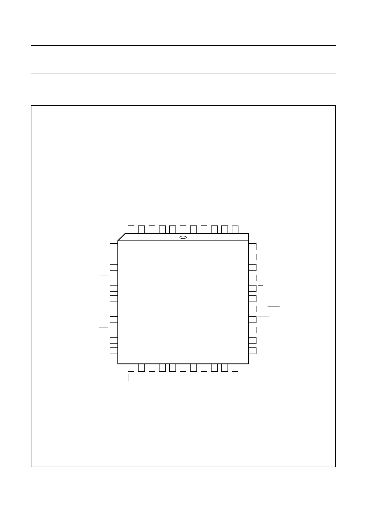
6 PINNING INFORMATION
6.1 Pinning diagram
Fig.3 Pinning Diagram for 44-lead LCC Package.
handbook, full pagewidth
P8xC591
MHI003
7
8
9
10
11
12
13
14
15
16
17
39
38
37
36
35
34
33
32
31
30
29
18
19
20
21
22
23
24
25
26
27
28
6
5
4
3
2
1
44
43
42
41
40
P1.4/ADC2/INT4/CT2I
P1.3/ADC1/INT3/CT1I
P1.2/ADC0/INT2/CT0I
P1.1/TXDC
P1.0/RXDC
AVSSAV
ref+
P0.0/AD0
P0.1/AD1
P0.2/AD2
P0.3/AD3
P3.6/WR
P3.7/RD
XTAL2
XTAL1
V
SS
V
DD
P2.0/A8
P2.1/A9
P2.2/A10
P2.3/A11
P2.4/A12
CT3I/INT5/ADC3/P1.5
SCL/ADC4/P1.6
SDA/ADC5/P1.7
RST
T2/P3.0/RXD
PWM0
RT2/P3.1/TXD
CMSR0/P3.2/INT0
CMSR1/P3.3/INT1
CMSR2/P3.4/T0
CMSR3/P3.5/T1
P0.4/AD4
P0.5/AD5
P0.6/AD6
P0.7/AD7
EA/V
PP
PWM1
ALE/PROG
PSEN
P2.7/A15
P2.6/A14
P2.5/A13

1999 Aug 19 8
Philips Semiconductors Objective Specification
Single-chip 8-bit microcontroller with CAN controller P8xC591
Fig.4 Pinning Diagram for 44-lead Plastic Quad Flat Package (QFP).
handbook, full pagewidth
P8xC591
MHI004
1
2
3
4
5
6
7
8
9
10
11
33
32
31
30
29
28
27
26
25
24
23
12
13
14
15
16
17
18
19
20
21
22
44
43
42
41
40
39
38
37
36
35
34
P1.4/ADC2/INT4/CT2I
P1.3/ADC1/INT3/CT1I
P1.2/ADC0/INT2/CT0I
P1.1/TXDC
P1.0/RXDC
AVSSAV
ref+
P0.0/AD0
P0.1/AD1
P0.2/AD2
P0.3/AD3
P3.6/WR
P3.7/RD
XTAL2
XTAL1
V
SS
V
DD
P2.0/A8
P2.1/A9
P2.2/A10
P2.3/A11
P2.4/A12
P1.5/ADC3/INT5/CT3I
P1.6/ADC4/SCL
P1.7/ADC5/SDA
RST
P3.0/T2/RXD
PWM0
RT2/P3.1/TXD
CMSR0/P3.2/INT0
CMSR2/P3.4/T0
CMSR3/P3.5/T1
P0.4/AD4
P0.5/AD5
P0.6/AD6
P0.7/AD7
EA/V
PP
PWM1
ALE/PROG
PSEN
P2.7/A15
P2.6/A14
P2.5/A13
CMSR1/P3.3/INT1

1999 Aug 19 9
Philips Semiconductors Objective Specification
Single-chip 8-bit microcontroller with CAN controller P8xC591
6.2 Pin description
Table 1 Pin description for QFP44/PLCC44, see Note 1.
SYMBOL
PIN
DESCRIPTION
QFP44 PLCC44
RST 4 10 Reset: A Input to reset the P8xC591. It also provides a reset pulse as output
when Timer T3 overflows.
P3.0to P3.7 Port 3 (P3.0 to P3.7): 8-bit programmable I/O port lines; Port 3 can
sink/source 4 LSTTL inputs.
Port 3 pins serve alternate functions as follows:
P3.0/RXD 5 11 RXD: Serial input port for UART;
T2: T2 event input
P3.1/TXD 7 13 TXD: Serial output port for UART;
RT2: T2 timer reset signal. Rising edge triggered.
P3.2/INT0/CMSR0 8 14 INT0: External interrupt input 0;
CMSR0: Compare and Set/Reset output for Timer T2.
P3.3/INT1/
CMSR1
915INT1: External interrupt input 1;
CMSR1: Compare and Set/Reset output for Timer T2.
P3.4/T0/CMSR2 10 16 T0: Timer 0 external interrupt input;
CMSR2: Compare and Set/Reset output for Timer T2.
P3.5/T1/CMSR3 11 17 T1: Timer 1 external interrupt input;
CMSR3: Compare and Set/Reset output for Timer T2.
P3.6/WR 12 18 WR: External Data Memory Write strobe;
P3.7/RD 13 19 RD: External Data Memory Read strobe.
During reset, Port 3 will be asynchronously driven resistive HIGH.
Port 3 has four modes selected on a per bit basis by writing to the P3M1 and
P3M2 registers as follows:
P3M1.x
0
0
1
1
P3M2.x
0
1
0
1
Mode Description
Pseudo-bidirectional (standard c51 configuration default)
Push-Pull
High impedance
Open drain
XTAL2 14 20 Crystal pin 2: output of the inverting amplifier that forms the oscillator. Left
open-circuit when an external oscillator clock is used.
XTAL1 15 21 Crystal pin 1: input to the inverting amplifier that forms the oscillator, and
input to the internal clock generator. Receives the external oscillator clock
signal when an external oscillator is used.
V
SS
16 22 Ground; circuit ground potential.
V
DD
17 23 Power supply; power supply pin during normal operation and power
reduction modes.

1999 Aug 19 10
Philips Semiconductors Objective Specification
Single-chip 8-bit microcontroller with CAN controller P8xC591
P2.0/A08 to
P2.7/A15
18 to 25 24 to 31 Port 2 (P2.0 to P2.7): 8-bit programmable I/O port lines;
A08 to A15: High-order address byte for external memory.
Alternate function: High-order address byte for external memory (A08-A15).
Port 2 is also used to input the upper order address during EPROM
programming and verification. A8 is on P2.0, A9 on P2.1, through A12 on
P2.4.
During reset, Port 2 will be asynchronously driven HIGH.
Port 2 has four output modes selected on a per bit basis by writing to the
P2M1 and P2M2 registers as follows:
P2M1.x
0
0
1
1
P2M2.x
0
1
0
1
Mode Description
Pseudo-bidirectional (standard c51 configuration default)
Push-Pull
High impedance
Open drain
PSEN 26 32 Program Store Enable output: read strobe to the external Program Memory
via Ports 0 and 2. Is activated twice each machine cycle during fetches from
external Program Memory. When executing out of external Program Memory
two activations of PSEN are skipped during each access to external Data
Memory. PSEN is not activated (remains HIGH) during no fetches from
external Program Memory. PSEN can sink/source 8 LSTTL inputs. It can
drive CMOS inputs without external pull-ups.
ALE/PROG 27 33 Address Latch Enable output. Latches the low byte of the address during
access of external memory in normal operation. It is activated every six
oscillator periods except during an external Data Memory access. ALE can
sink/source 8 LSTTL inputs. It can drive CMOS inputs without an external
pull-up. To prohibit the toggling of ALE pin (RFI noise reduction) the bit A0
(SFR: AUXR.0) must be set by software; see Table 4.
PROG: the programming pulse input; alternative function for the P87C591.
EA/V
PP
29 35 External Access input. If, during reset, EA is held at a TTL level HIGH the
CPU executes out of the internal Program Memory. If, during reset, EA is held
at a TTL level LOW the CPU executes out of external Program Memory via
Port 0 and Port 2. EA is not allowed to float. EA is latched during reset and
don’t care after reset.
VPP: the programming supply voltage; alternative function for the P87C591.
P0.0/AD0 to
P0.7/AD7
30 to 37 36 to 43 Port 0: 8-bit open-drain bidirectional I/O port.
During reset, Port 0 is HIGH-Impedance (Tri-State).
AD7 to AD0: Multiplexed Low-order address and Data bus for external
memory. During these accesses internal pull-ups are activated. Port 0 can
sink/source up to 8 LSTTL inputs.
AV
ref+
38 44 Analog to Digital Conversion Reference Resistor: High-end.
AV
SS
39 1 Analog ground.
SYMBOL
PIN
DESCRIPTION
QFP44 PLCC44

1999 Aug 19 11
Philips Semiconductors Objective Specification
Single-chip 8-bit microcontroller with CAN controller P8xC591
Notes
1. To avoid “latch-up” effect as power-on, the voltage on any pin at any time must not be higher or lower than VDD+0.5 V
or VSS−0.5 V.
2. Not implemented for P1.6 and P1.7.
P1.0 to P1.4
P1.5 to P1.7
40 to 44
1to3
2to6
7to9
Port 1: 8-bit I/O port with a user configurable output type. The operation of
Port 1 pins as inputs or outputs depends upon the port configuration selected.
Each port pin is configured independently.
Port 1 also provides various special functions as described below:
P1.0 40 2 RXDC: CAN Receiver input line.
P1.1 41 3 TXDC: CAN Transmit output line.
During reset, Port P1.0 and P1.1 will be asynchronously driven resistive
HIGH, P1.2 to P1.7 is High-Impedance (Tri-state).
P1.2 to P1.4 42 to 44 4 to 6 CT0I/INT2 / CT1I/INT3 / CT2I/INT4: T2 Capture timer inputs or External
Interrupt inputs.
P1.5 to P1.7 1 to 3 7 to 9
ADC0 to ADC2: Alternate function: Input channels to ADC.
ADC3 to ADC5: Input channels to ADC:
P1.5 1 7 CT3I/INT5: T2 Capture timer input or External Interrupt inputs.
P1.6 2 8 SCL: Serial port clock line I2C.
P1.7 3 9 SDA: Serial data clock line I2C.
Port 1 has four modes selected on a per bit basis by writing to the P1M1 and
P1M2 registers as follows:
P1M1.x
0
0
1
1
P1M2.x
0
1
0
1
Mode Description
Pseudo-bidirectional (standard c51 configuration default
(2)
)
Push-Pull
(2)
High impedance
Open drain
Port 1 is also used to input the lower order address byte during EPROM
programming and verification. A0 is on P1.0, etc.
PWM0 6 12 Pulse Width Modulation: Output 0.
PWM1 28 34 Pulse Width Modulation: Output 1.
SYMBOL
PIN
DESCRIPTION
QFP44 PLCC44
1999 Aug 19 12
Philips Semiconductors Objective Specification
Single-chip 8-bit microcontroller with CAN controller P8xC591
7 MEMORY ORGANIZATION
The Central Processing Unit (CPU) manipulates operands in three memory spaces as follows (see Fig.5):
• 16 kbytes internal resp. 64 kbytes external Program Memory
• 512 bytes internal Data Memory Main-and Auxiliary RAM
• up to 64 kbytes external Data Memory (with 256 bytes residing in the internal Auxiliary RAM).
Fig.5 Memory map and address space with EXTRAM = 0.
handbook, full pagewidth
MHI005
INDIRECT ONLY
DIRECT AND
INDIRECT
AUXILIARY
RAM
(EXTRAM = 0)
SFRs
255
127
0
EXTERNAL
(EA = 0)
INTERNAL
(EA = 1)
MAIN RAM
INTERNAL DATA MEMORY
EXTERNAL
DATA MEMORY
PROGRAM MEMORY
EXTERNAL
64K
64K
16384
16383
0
OVERLAPPED SPACE
256

1999 Aug 19 13
Philips Semiconductors Objective Specification
Single-chip 8-bit microcontroller with CAN controller P8xC591
7.1 Program Memory
The P8xC591 contains 16 Kbytes of on-chip Program
Memory which can be extended to 64 Kbytes with external
memories. When EA pin is held HIGH, the P8xC591
fetches instructions from internal ROM unless the address
exceeds 3FFFh. Locations 4000h to FFFFh are fetched
from external Program Memory. When the EA pin is held
LOW, all instruction fetches are from external memory.
The EA pin is latched during reset and is “don’t care” after
reset.
Both, for the ROM and EPROM version of the P8xC591,
precautions are implemented to protect the device against
illegal Program Memory code reading.
7.2 Addressing
The P8xC591 has five methods for addressing the
Program and Data memory:
• Register
• Direct
• Register-Indirect
• Immediate
• Base-Register plus Index-Register-Indirect.
For more details about Addressing modes please refer to
Section 22.1 “Addressing Modes”.
7.3 Expanded Data RAM addressing
The P8xC591 has internal data memory that is mapped
into four separate segments: the lower 128 bytes of RAM,
upper 128 bytes of RAM, 128 bytes Special Function
Register (SFR), and 256 bytes Auxiliary RAM (AUX-RAM)
as shown in Figure 5.
The four segments are:
1. The Lower 128 bytes of RAM (addresses 00H to 7FH)
are directly and indirectly addressable (see Fig.6).
2. The Upper 128 bytes of RAM (addresses 80H to FFH)
are indirectly addressable.
3. The Special Function Registers, SFRs, (addresses
80H to FFH) are directly addressable only. All these
SFRs are described in Table 4.
4. The 256-bytes AUX-RAM (00H - FFH) are indirectly
accessed by move external instruction, MOVX, and
within the EXTRAM bit cleared, see Table 3.
The Lower 128 bytes can be accessed by either direct or
indirect addressing. The Upper 128 bytes can be
accessed by indirect addressing only. The Upper 128
bytes occupy the same address space as the SFR. That
means they have the same address, but are physically
separate from SFR space.
When an instruction accesses an internal location above
address 7FH, the CPU knows whether the access is to the
upper 128 bytes of data RAM or to SFR space by the
addressing mode used in the instruction. Instructions that
use direct addressing access SFR space.
For example:
MOV 0A0H,#data
accesses the SFR at location 0A0H (which is P2).
Instructions that use indirect addressing access the Upper
128 bytes of data RAM.
For example:
MOV @ R0,#data
where R0 contains 0A0H, accesses the data byte at
address 0A0H, rather than P2 (whose address is 0A0H).
The AUX-RAM can be accessed by indirect addressing,
with EXTRAM bit cleared and MOVX instructions. This
part of memory is physically located on-chip, logically
occupies the first 256-bytes of external data memory.
With EXTRAM = 0, the AUX-RAM is indirectly addressed,
using the MOVX instruction in combination with any of the
registers R0, R1 of the selected bank or DPTR. An access
to AUX-RAM will not affect ports P0, P3.6 (WR#) and P3.7
(RD#). P2 SFR is output during external addressing. For
example, with EXTRAM = 0,
MOV @ R0,#data
where R0 contains 0A0h, access the AUX-RAM at
address 0A0H rather than external memory. An access to
external data memory locations higher than FFH (i.e.,
0100H to FFFFH) will be performed with the MOVX DPTR
instructions in the same way as in the standard 80C51, so
with P0 and P2 as data/address bus, and P3.6 and P3.7
as write and read timing signals. Refer to Table 4.
With EXTRAM = 1, MOVX @ Ri and MOVX @ DPTR will
be similar to the standard 80C51. MOVX @ Ri will provide
an 8-bit address multiplexed with data on Port 0 and any
output port pins can be used to output higher order
address bits. This is to provide the external paging
capability. MOVX @ DPTR will generate a 16-bit address.
Port 2 outputs the high-order eight address bits (the
contents of DPH) while Port 0 multiplexes the low-order
eight address bits (DPL) with data. MOVX @ Ri and MOVX
@ DPTR will generate either read or write signals on P3.6
(#WR) and P3.7 (#RD).
The stack pointer (SP) may be located anywhere in the
256 bytes RAM (lower and upper RAM) internal data
memory. The stack cannot be located in the AUX-RAM.

1999 Aug 19 14
Philips Semiconductors Objective Specification
Single-chip 8-bit microcontroller with CAN controller P8xC591
Table 2 AUX-RAM Page Register (address 8EH)
Table 3 Description of AUX-RAM bits
Notes
1. User software should not write ‘1’s to reserved bits. These bits may be used in future 80C51 family products to invoke
new features. In that case, the reset or inactive of the new bit will be 0, and its active value will be ‘1’. The value read
from a reserved bit is indeterminate.
2. Reset value is ‘xxxxxx10B’.
76543210
- - - - - LVADC EXTRAM AO
BIT SYMBOL FUNCTION
7 to 3 − Reserved for future use; see Note 1.
2 LVADC Enable A/D low voltage operation.
LVADC
0
1
Operating Mode
Turns off A/D charge pump.
Turns on A/D charge pump. Required for operation below 4 V.
1 EXTRAM Internal/External RAM (00H - FFH) access using MOVX @ RI / @ DPTR
EXTRAM
0
1
Operating Mode
Internal AUX-RAM (00H - FH) access using MOVX @ RI / @ DPTR.
External data memory access.
0 AO Disable/Enable ALE.
AO
0
1
Operating Mode
ALE is permitted at a constant rate of 1/6 the oscillator frequency.
ALE is active only during a MOVX or MOVC instruction.

1999 Aug 19 15
Philips Semiconductors Objective Specification
Single-chip 8-bit microcontroller with CAN controller P8xC591
Fig.6 Internal Main RAM bit addresses.
handbook, full pagewidth
MHI006
7F 7E 7D 7C 7B 7A 79 78
77 76 75 74 73 72 71 70
6F 6E 6D 6C 6B 6A 69 68
67 66 65 64 63 62 61 60
5F 5E 5D 5C 5B 5A 59 58
57 56 55 54 53 52 51 50
4F 4E 4D 4C 4B 4A 49 48
47 46 45 44 43 42 41 40
3F 3E 3D 3C 3B 3A 39 38
37 36 35 34 33 32 31 30
2F 2E 2D 2C 2B 2A 29 28
27 26 25 24 23 22 21 20
1F 1E 1D 1C 1B 1A 19 18
17 16 15 14 13 12 11 10
0F 0E 0D 0C 0B 0A 09 08
07 06 05 04 03 02 01 00
18h
17h
10h
0Fh
08h
07h
00h
24
23
31
16
15
8
7
0
REGISTER BANK 3
REGISTER BANK 2
REGISTER BANK 1
REGISTER BANK 0
32
33
34
35
36
37
38
39
40
41
42
43
44
45
46
47
(MSB) (LSB)
127
7Fh
2Fh
2Eh
2Dh
2Ch
2Bh
2Ah
29h
28h
27h
26h
25h
24h
23h
22h
21h
20h
1Fh
1999 Aug 19 16
Philips Semiconductors Objective Specification
Single-chip 8-bit microcontroller with CAN controller P8xC591
7.3.1 SPECIAL FUNCTION REGISTERS
Table 4 Special Function Register Bit Address, Symbol or Alternate Port Function
* = SFRs are bit addressable; # = SFRs are modified from or added to the 80C51 SFRs.
NAME DESCRIPTION
SFR
ADDR
BIT FUNCTIONS AND ADDRESSES
RESET
VALUE
MSB LSB
ACC* Accumulator E0H E7 E6 E5 E4 E3 E2 E1 E0 00H
ADCH# A/D converter high C6H xxxxxxxxb
ADCON# A/D control C5H ADC.1 ADC.0 - ADCI ADCS AADR2 AADR1 AADR0 xx000000b
AUXR Auxiliary 8EH - - - - - LVADC EXTRAM A0 xxxxx110B
AUXR1 Auxiliary A2H ADC8 AIDL SRST WDE WUPD 0 - DPS 000000x0B
B* B register F0H F7 F6 F5 F4 F3 F2 F1 F0 00H
CTCON# Capture control EBH CTN3 CTP3 CTN2 CTP2 CTN1 CTP1 CTN0 CTP0 00H
CTH3# Capture high 3 CFH xxxxxxxxB
CTH2# Capture high 2 CEH xxxxxxxxB
CTH1# Capture high 1 CDH xxxxxxxxB
CTH0# Capture high 0 CCH xxxxxxxxB
CMH2# Compare high 2 CBH 00H
CMH1# Compare high 1 CAH 00H
CMH0# Compare high 0 C9H 00H
CTL3# Capture low 3 AFH xxxxxxxxB
CTL2# Capture low 2 AEH xxxxxxxxB
CTL1# Capture low 1 ADh xxxxxxxxB
CTL0# Capture low 0 ACH xxxxxxxxB
CML2# Compare low 2 ABH 00H
CML1# Compare low 1 AAH 00H
CML0# Compare low 0 A9H 00H
DPTR: Data Pointer (2 bytes):
DPH Data Pointer High 83h 00H
DPL Data Pointer Low 82h 00H
AF AE AD AC AB AA A9 A8
IENO*# Interrupt Enable 0 A8H EA EAD ES1 ES0 ET1 EX1 ET0 EX0 00H
EF EE ED EC EB EA E9 E8
IEN1*# Interrupt Enable 1 E8H ET2 ECAN ECM1 ECM0 ECT3 ECT2 ECT1 ECT0 00H
BF BE BD BC BB BA B9 B8
IP0*# Interrupt Priority 0 B8H - PAD PS1 PS0 PT1 PX1 PT0 PX0 x0000000B
FF FE FD FC FB FA F9 F8
IP0H Interrupt Priority 0 high B7H - PADH PS1H PS0H PT1H PX1H PT0H PX0H x0000000B
IP1*# Interrupt Priority 1 F8h PT2 PCAN PCM1 PCM0 PCT3 PCT2 PCT1 PCT0 00H
IP1H Interrupt Priority 1 high F7H PT2H PCANH PCM1H PCM0H PCT3H PCT2H PCT1H PCT0H 00H
CANMOD CAN Mode Register C4H 00H
CANCON CAN Command (w) and
Interrupt (r)
C3H 00H
CANDAT CAN Data C2H 00H
CANADR CAN Address C1H 00H
C7 C6 C5 C4 C3 C2 C1 C0
CANSTA CAN Status (r) C0H BS ES TS RS TCS TBS DOS RBS 00H
CAN Interrupt Enable (w) BEIE ALIE EPIE WUIE DOIE EIE TIE RIE

1999 Aug 19 17
Philips Semiconductors Objective Specification
Single-chip 8-bit microcontroller with CAN controller P8xC591
P1M1 Port 1 output mode 1 92H FCH
P1M2 Port 1 output mode 2 93H 00H
P2M1 Port 2 output mode 1 94H 00H
P2M2 Port 2 output mode 2 95H 00H
P3M1 Port 3 output mode 1 9AH 00H
P3M2 Port 3 output mode 2 9BH 00H
B7 B6 B5 B4 B3 B2 B1 B0
- - CSMR3 CSMR2 CSMR1 CSMR0 RT2 T2
P3* Port 3 B0H RD WR T1 T0 INT1 INT0 TXD RXD FFH
A7 A6 A5 A4 A3 A2 A1 A0
P2* Port 2 A0H A15 A14 A13 A12 A11 A10 A9 A8 FFH
97 96 95 94 93 92 91 90
ADC5 ADC4 ADC3 ADC2 ADC1 ADC0 −−
P1* Port 1 90H SDA SCL CT3I CT2I CT1I CT0I TXDC RXDC FFH
87 86 85 84 83 82 81 80
P0* Port 0 80H AD7 AD6 AD5 AD4 AD3 AD2 AD1 AD0 FFH
PCON Power Control 87H SMOD1 SMOD0 POF WLE GF1 GF0 PD IDL 00x00000B
PSW Program Status Word D0H CY AC F0 RS1 RS0 OV F1 P 00H
PWMP# PWM Prescaler FEH 00H
PWMP1# PWM Register 1 FDH 00H
PWMP0# PWM Register 0 FCH 00H
RTE# Reset Enable EFH RP35 RP34 RP33 RP32 xxxx0000B
S0ADDR Serial 0 Slave Address CBh 00H
S0ADEN Slave Address Mask F9H 00H
SP Stack Pointer 81H 07H
S0BUF Serial 0 Data Buffer 99H xxxxxxxxB
S0PSL Prescaler Value UART FAH 00H
S0PSH Prescaler/Value UART FBH SPS Prescaler higher nibble 0xxx0000B
9F 9E 9D 9C 9B 9A 99 98
S0CON* Serial 0 Control 98H SM0/FE SM1 SM2 REN TB8 RB8 TI RI 00H
S1CON#* Serial 1Control D8H CR2 ENS1 STA ST0 SI AA CR1 CR0 00H
S1ADR# Serial 1 Address DBH SLAVE ADDRESS GC 00H
S1DAT# Serial 1 Data DAH 00H
S1STA# Serial 1 Status D9H SC4 SC3 SC2 SC1 SC0 0 0 0 F8H
DF DE DD DC DB DA D9 D8
STE# Set Enable EEH SP35 SP34 SP33 SP32 xxxx0000B
TH1 Timer High 1 8DH 00H
TH0 Timer High 0 8CH 00H
TL1 Timer Low 1 8BH 00H
TL0 Timer Low 0 8AH 00H
TMH2# Timer High 2 EDH 00H
TML2# Timer Low 2 ECH 00H
NAME DESCRIPTION
SFR
ADDR
BIT FUNCTIONS AND ADDRESSES
RESET
VALUE
MSB LSB

1999 Aug 19 18
Philips Semiconductors Objective Specification
Single-chip 8-bit microcontroller with CAN controller P8xC591
TMOD Timer Mode 89H GATE C/T M1 M0 GATE C/T M1 M0 00H
8F 8E 8D 8C 8B 8A 89 88
TCON* Timer Control 88H TF1 TR1 TF0 TR0 IE1 IT1 IE0 IT0 00H
TM2CON# Timer 2 Control EAH T2IS1 T2IS0 T2ER T2B0 T2P1 T2P0 T2MS1 T2MS0 00H
CF CE CD CC CB CA C9 C8
TM2IR#* Timer 2/CAN Int Flag Reg C8H T2OV CMI2/
CAN
CMI1 CMI0 CTI3 CTI2 CTI1 CTI0 00H
T3# Timer 3 FFH 00H
NAME DESCRIPTION
SFR
ADDR
BIT FUNCTIONS AND ADDRESSES
RESET
VALUE
MSB LSB

1999 Aug 19 19
Philips Semiconductors Objective Specification
Single-chip 8-bit microcontroller with CAN controller P8xC591
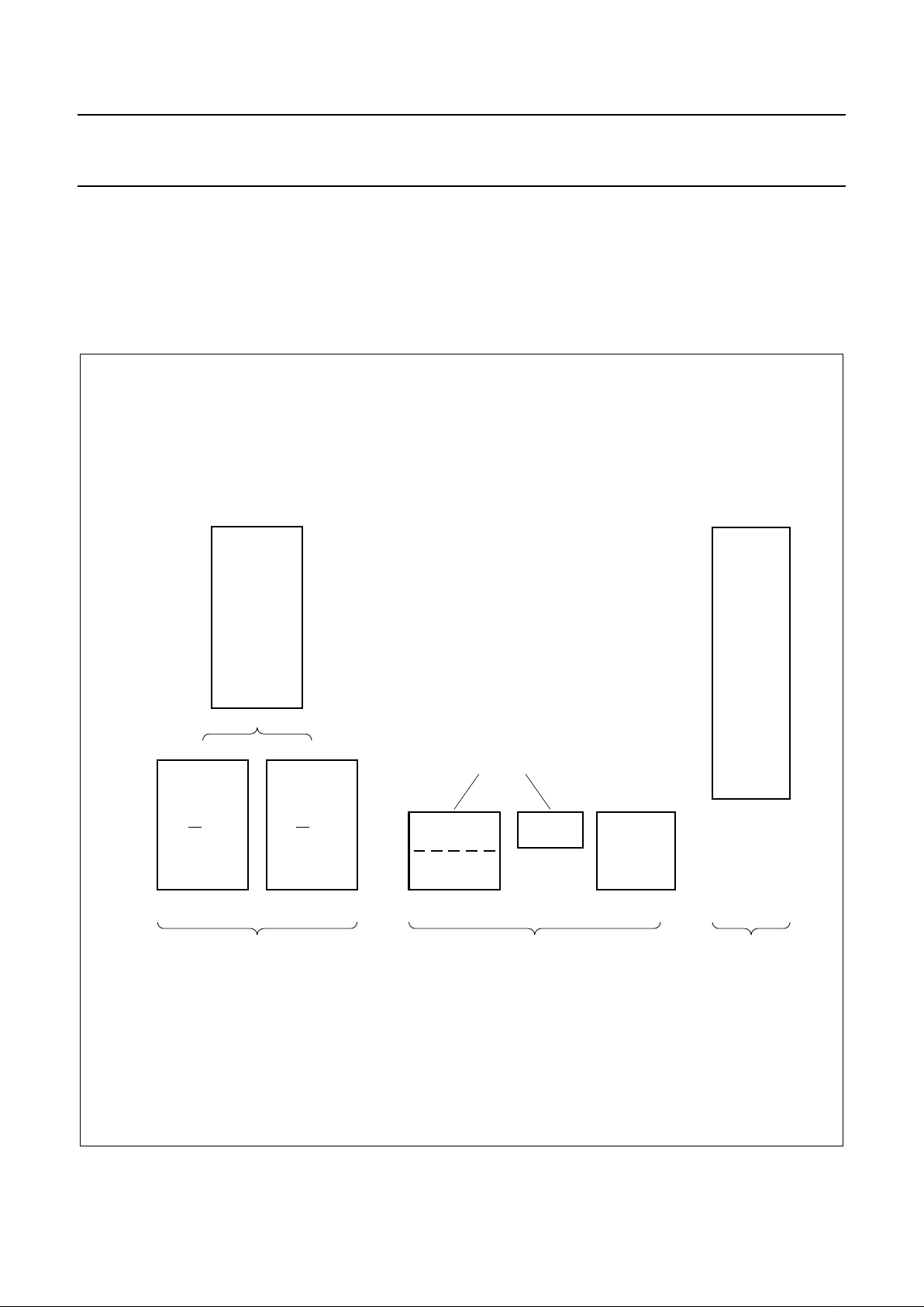
Fig.7 Dual DPTR:
handbook, full pagewidth
DPH
(83H)
BT0
AUXR1
DPS
DPL
(82H)
EXTERNAL
DATA
MEMORY
DPTR0
MHI007
DPTR1
7.4 Dual DPTR
The dual DPTR structure (see Figure 7) is a way by which
the chip will specify the address of an external data
memory location. There are two 16-bit DPTR registers that
address the external memory, and a single bit called DPS
= AUXR1/bit0 that allows the program code to switch
between them.
The DPS bit status should be saved by software when
switching between DPTR0 and DPTR1.
Note that bit 2 is not writable and is always read as a zero.
This allows the DPS bit to be quickly toggled simply by
executing an INC AUXR1 instruction without affecting the
other bits.
DPTR Instructions
The instructions that refer to DPTR refer to the data pointer
that is currently selected using the AUXR1/bit 0 register.
The six instructions that use the DPTR are as follows:
INC DPTRIncrements the data pointer by 1
MCV DPTR, #data 16 Loads the DPTR with a 16-bit
constant
MOV A, @ A+DPTR Move code byte relative to
DPTR to ACC
MOVX A, @ DPTR Move external RAM (16-bit
address) to ACC
MOVX @ DPTR, A Move ACC to external RAM
(16-bit address)
JMP @ A + DPTR Jump indirect relative to
DPTR
The data pointer can be accessed on a byte-by-byte basis
by specifying the low or high byte in an instruction which
accesses the SFRs. See application note AN458 for more
details.

1999 Aug 19 20
Philips Semiconductors Objective Specification
Single-chip 8-bit microcontroller with CAN controller P8xC591
7.4.1 AUXR1 PAGE REGISTER
Table 5 AUXR1 Page Register (address A2H)
Table 6 Description of AUXR1 of bits
User software should not write 1s to reserved bits. Theses bits may be used in future 8051 family products to invoke
new features. In that case, the reset or inactive value of the new bit will be logic 0, and its active value will be logic 1.
The value read from a reserved bit is indeterminate. The reset value of AUXR1 is (000000xB).
76543210
ADC8 AIDL SRST WDE WUPD 0 − DSP
BIT SYMBOL DESCRIPTION
7 ADC8 ADC Mode Switch. Switches between 10-bit conversion and 8-bit conversion
ADC8
0
1
Operating Mode
10-bit conversion (50 machine cycles)
8-bit conversion (24 machine cycles)
6 AIDL Enables the ADC during Idle mode.
5 SRST Software Reset.
4 WDE Watchdog Timer Enable Flag.
3 WUPD Enable Wake-up from Power-down.
20Reserved.
1 − Reserved.
0 DSP Data Pointer Switch. Switches between DPRT0 and DPTR1.
ADC8
0
1
Operating Mode
DPTR0
DPTR1
1999 Aug 19 21
Philips Semiconductors Objective Specification
Single-chip 8-bit microcontroller with CAN controller P8xC591
8 I/O FACILITIES
The P8xC591 consists of 32 I/O Port lines with partly
multiple functions. The I/O’s are held HIGH during reset
(asynchronous, before oscillator is running).
Ports 0, 1, 2 and 3 perform the following alternative
functions:
Port 0 is the same as in the 80C51. After reset the Port
Special Function Register is set to ’FFh’ as known
from other 80C51 derivatives. Port 0 also provides
the multiplexed low-order address and data bus
used for expanding the P8xC591 with standard
memories and peripherals.
Port 1 supports several alternative functionalities. For this
reason it has different I/O stages. Note, port P1.0
and P1.1 are Driven-High and P1.2 to P1.7 are
High-Impedance (Tri-state) after reset.
Port 2 is the same as in the 80C51. After reset the Port
Special Function Register is set to ’FFh’ as known
from other 80C51 derivatives. Port 2 also provides
the high-order address bus when the P8xC591 is
expanded with external Program Memory and/or
external Data Memory.
Port 3 is the same as in the 80C51. During reset the Port
3 Special Function Register is set to ’FFh’ as known
from other 80C51 derivatives.
9 OSCILLATOR CHARACTERISTICS
XTAL1 and XTAL2 are the input and output, respectively,
of an inverting amplifier. The pins can be configured for
use as an on-chip oscillator, as shown in the logic symbol.
To drive the device from an external clock source, XTAL1
should be driven while XTAL2 is left unconnected. There
are no requirements on the duty cycle of the external clock
signal. However, minimum and maximum high and low
times specified in the data sheet must be observed.
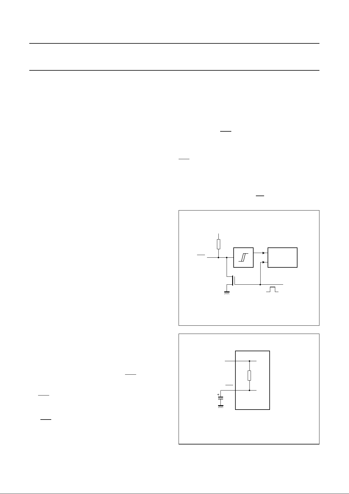
10 RESET
A reset is accomplished by holding the RST pin LOW for
at least two machine cycles (12 oscillator periods), while
the oscillator is running. To insure a good power-on reset,
theRST pin must be low long enough to allow the oscillator
time to start up (normally a few milliseconds) plus two
machine cycles.
The RST line can also be pulled LOW internally by a
pull-down transistor activated by the watchdog timer T3.
The length of the output pulse from T3 is 3 machine cycles.
A pulse of such short duration is necessary in order to
recover from a processor or system fault as fast as
possible.
Note that the short reset pulse from Timer T3 cannot
discharge the power-on reset capacitor (see Figure 8).
Consequently, when the watchdog timer is also used to set
external devices, this capacitor arrangement should not be
connected to the RST pin, and a different circuit should be
used to perform the power-on reset operation. A timer T3
overflow, if enabled, will force a reset condition to the
P8xC591 by an internal connection, whether the output
RST is pulled-up HIGH or not.
A reset may be performed in software by setting the
software reset bit, SRST (AUXR1.5).
This device also has a Power-on Detect Reset circuit as
VCC transitions from VCC past V
RST
.
Fig.8 On-Chip Reset Configuration.
handbook, halfpage
MHI008
SCHMITT
TRIGGER
RESET
CIRCUITRY
RST
overflow
timer T3
on-chip
resistor
V
DD
Fig.9 Power-on Reset.
handbook, halfpage
MHI009
RST
R
RST
2.2 µF
P8xC591
V
DD

1999 Aug 19 22
Philips Semiconductors Objective Specification
Single-chip 8-bit microcontroller with CAN controller P8xC591
11 LOW POWER MODES
11.1 Stop Clock Mode
The static design enables the clock speed to be reduced
down to 0 MHz (stopped). When the oscillator is stopped,
the RAM and Special Function Registers retain their
values. This mode allows step-by-step utilization and
permits reduced system power consumption by lowering
the clock frequency down to any value. For lowest power
consumption the Power-down mode is suggested.
11.2 Idle Mode
In the Idle mode (see Table 7), the CPU puts itself to sleep
while all of the on-chip peripherals stay active. The
instruction to invoke the idle mode is the last instruction
executed in the normal operating mode before the Idle
mode is activated. The CPU contents, the on-chip RAM,
and all of the special function registers remain intact during
this mode. The Idle mode can be terminated either by any
enabled interrupt (at which time the process is picked up
at the interrupt service routine and continued), or by a
hardware reset which starts the processor in the same
manner as a Power-on reset.
11.3 Power-down Mode
To save even more power, a Power-down mode (see
Table 7) can be invoked by software. In this mode, the
oscillator is stopped and the instruction that invoked Power
Down is the last instruction executed. The on-chip RAM
and Special Function Registers retain their values down to
2.0 V and care must be taken to return VCCto the minimum
specified operating voltages before the Power-down Mode
is terminated.
A hardware reset or external interrupt can be used to exit
from Power-down. The Wake-up from Power-down bit,
WUPD (AUXR1.3) must be set in order for an interrupt to
cause a Wake-up from Power-down. Reset redefines all
the SFRs but does not change the on-chip RAM. A
Wake-up allows both the SFRs and the on-chip RAM to
retain their values.
To properly terminate Power-down the reset or external
interrupt should not be executed before VCC is restored to
its normal operating level and must be held active long
enough for the oscillator to restart and stabilize (normally
less than 10 ms).
Table 7 Status of external pins during Idle and Power-down modes
With an external interrupt, INT0 and INT1 must be enabled and configured as level-sensitive. Holding the pin low restarts
the oscillator but bringing the pin back high completes the exit. Once the interrupt is serviced, the next instruction to be
executed after RETI will be the one following the instruction that put the device into Power-down.
MODE MEMORY ALE PSEN PORT 0 PORT 1 PORT 2 PORT 3
PWM0/
PWM1
Idle internal 1 1 port data port data port data port data high
external 1 1 float port data address port data high
Power-down internal 0 0 port data port data port data port data high
external 0 0 float port data port data port data high

1999 Aug 19 23
Philips Semiconductors Objective Specification
Single-chip 8-bit microcontroller with CAN controller P8xC591
11.3.1 POWER OFF FLAG
The Power Off Flag (POF) is set by on-chip circuitry when
the VCC level on the P8xC591 rises from 0 to 5 V. The POF
bit can be set or cleared by software allowing a user to
determine if the reset is the result of a power-on or warm
after Power-down. The VCC level must remain above 3 V
for the POF to remain unaffected by the VCC level.
11.3.2 DESIGN CONSIDERATION
• When the Idle mode is terminated by a hardware reset,
the device normally resumes program execution, from
where it left off, up to two machine cycles before the
internal reset algorithm takes control. On-chip hardware
inhibits access to internal RAM in this event, but access
to the port pins is not inhibited. To eliminate the
possibility of an unexpected write when Idle is
terminated by reset, the instruction following the one
that invokes Idle should not be one that writes to a port
pin or to external memory.
11.3.3 ONCE
TM
MODE
The ONCETM (“On-Circuit Emulation”) Mode facilities
testing and debugging of systems without the device
having to be removed from the circuit. The ONCE Mode is
invoked by:
1. Pull ALE low while the device is in reset an PSEN is
high,
2. Hold ALE low as RST is deactivated.
While the device is in ONCE Mode, the Port 0 pins go into
a float state, and the other port pins and ALE and PSEN
are weakly pulled high. The oscillator circuit remains
active. While the device is in this mode, an emulator or test
CPU can be used to drive the circuit. Normal operation is
restored when a normal reset is applied.
11.3.4 REDUCED EMI MODE
The ALE-Off bit, AO (AUXR.0) can be set to 0 disable the
ALE output. It will automatically become active when
required for external memory accesses and resume to the
OFF state after completing the external memory access.
11.3.5 P
OWER CONTROL REGISTER (PCON)
Table 8 Power Control Register (address 87H)
Table 9 Description of PCON bits
If logic 1s are written to PD and IDL at the same time, PD takes precedence. The reset value of PCON is (0XX00000).
76543210
SMOD1 SMOD0 POF WLE GF1 GF0 PD IDL
BIT SYMBOL DESCRIPTION
7 SMOD1 Double Baud rate. When set to logic 1 the baud rate is doubled when the serial port
SIO0 is being used in Modes 1, 2 and 3.
6 SMOD0 Double Baud rate. Selects SM0/FE for SCON.7 bit.
5 POF Power Off flag.
4 WLE Watchdog Load Enable. This flag must be set by software prior to loading T3
(Watchdog Timer). It is cleared when T3 is loaded.
3 GF1 General purpose flag bits.
2 GF0
1PDPower-down mode select. Setting this bit activates Power-down mode. It can only be
set if the Watchdog timer enable bit ‘WDE’ is set to logic 0.
0 IDL Idle mode select. Setting this bit activates the Idle mode.

1999 Aug 19 24
Philips Semiconductors Objective Specification
Single-chip 8-bit microcontroller with CAN controller P8xC591
12 CAN, CONTROLLER AREA NETWORK
Controller Area Network is the definition of a high
performance communication protocol for serial data
communication. The CAN controller circuitry is designed to
provide a full implementation of the CAN-Protocol
according to the CAN Specification Version 2.0 B.
Microcontroller including this on-chip CAN Controller are
used to build powerful local networks, both for general
industrial and automotive environments. The result is a
strongly reduced wiring harness and enhanced diagnostic
and supervisory capabilities.
The P8xC591 includes the same functions known from the
SJA1000 stand-alone CAN Controller from Philips
Semiconductors with the following improvements:
• Enhanced receive interrupt
• Enhanced acceptance filter
– 8 filter for standard frame formats
– 4 filter for extended formats
– “change on the fly” feature.
12.1 Features of the PeliCAN Controller
12.1.1 GENERAL CAN FEATURES
• CAN 2.0B protocol compatibility
• Multi-master architecture
• Bus access priority determined by the message
identifier (11 bit or 29 bit)
• Non destructive bit-wise arbitration
• Guaranteed latency time for high priority messages
• Programmable transfer rate (up to 1Mbit/s)
• Multicast and broadcast message facility
• Data length from 0 up to 8 bytes
• Powerful error handling capability
• Non-return-to-zero (NRZ) coding/decoding with
bit-stuffing
• Suitable for use in a wide range of networks including
SAE’s network classes A, B, C.
12.1.2 P8XC591 PELICAN FEATURES (ADDITIONAL TO
CAN 2.0B)
• Supports 11-bit identifier as well as 29-bit identifier
• Bit rates up to 1 Mbit/s
• Error Counters with read / write access
• Programmable Error Warning Limit
• Arbitration Lost Interrupt with detailed bit position
• Single Shot Transmission (no re-transmission)
• Listen Only Mode (no acknowledge, no active error
flags)
• Hot Plugging support (software driven bit rate detection)
• Extended receive buffer (FIFO, 64 byte)
• Receive Buffer level sensitive Receive Interrupt
• High Priority Acceptance Filters for Receive Interrupt
• Acceptance Filters with “change on the fly” feature
• Reception of “own” messages (Self Reception Request)
• Programmable CAN output driver configuration
1999 Aug 19 25
Philips Semiconductors Objective Specification
Single-chip 8-bit microcontroller with CAN controller P8xC591
12.2 PeliCAN structure
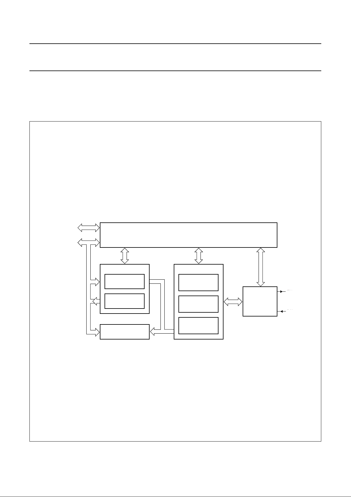
A 80C51 CPU Interface connects the PeliCAN to the internal bus of the P8xC591 microcontroller. Via five Special
Function Registers CANADR, CANDAT, CANMOD, CANSTA and CANCON the CPU has access to the PeliCAN. The
SFR will described later on.
Fig.10 Block Diagram of the PeliCAN.
handbook, full pagewidth
MHI010
PeliCAN Core BlockMESSAGE BUFFER
ERROR
MANAGEMENT
LOGIC
TRANSMIT
BUFFER
control
address/data
RECEIVE
FIFO
ACCEPTANCE
FILTER
BIT
TIMING
LOGIC
TRANSMIT
MANAGEMENT
LOGIC
INTERFACE
MANAGEMENT
LOGIC
TX
RX
BIT
STREAM
PROCESSOR
TXDC
RXDC

1999 Aug 19 26
Philips Semiconductors Objective Specification
Single-chip 8-bit microcontroller with CAN controller P8xC591
12.2.1 INTERFACE MANAGEMENT LOGIC (IML)
The Interface Management Logic interprets commands
from the CPU, controls addressing of the CAN Registers
and provides interrupts and status information to the CPU.
Additionally it drives the universal interface of the PeliCAN.
12.2.2 TRANSMIT BUFFER (TXB)
The Transmit Buffer is an interface between the CPU and
the Bit Stream Processor (BSP) and is able to store a
complete CAN message which should be transmitted over
the CAN network. The buffer is 13 bytes long, written by
the CPU and read out by the BSP or the CPU itself.
12.2.3 RECEIVE BUFFER (RXB, RXFIFO)
The Receive Buffer is an interface between the
Acceptance Filter and the CPU and stores the received
and accepted messages from the CAN Bus line. The
Receive Buffer (RXB) represents a CPU-accessible
13-byte-window of the Receive FIFO (RXFIFO), which has
a total length of 64 bytes depending on the
implementation. With the help of this FIFO the CPU is able
to process one message while other messages are being
received.
12.2.4 ACCEPTANCE FILTER (ACF)
The Acceptance Filter compares the received identifier
with the Acceptance Filter Table contents and decides
whether this message should be accepted or not. In case
of a positive acceptance test, the complete message is
stored in the RXFIFO. The ACF contains 4 independent
Acceptance Filter banks supporting extended and
standard CAN frames with “change on the fly” feature.
12.2.5 B
IT STREAM PROCESSOR (BSP)
The Bit Stream Processor is a sequencer, controlling the
data stream between the Transmit Buffer, RXFIFO and the
CAN-Bus. It also performs the error detection, arbitration,
stuffing and error handling on the CAN bus.
12.2.6 ERROR MANAGEMENT LOGIC (EML)
The EML is responsible for the error confinement of the
transfer-layer modules. It gets error announcements from
the BSP and then informs the BSP and IML about error
statistics.
12.2.7 B
IT TIMING LOGIC (BTL)
The Bit Timing Logic monitors the serial CAN bus line and
handles the Bus line-related bit timing. It synchronizes to
the bit stream on the CAN Bus on a “recessive” to
“dominant” Bus line transition at the beginning of a
message (hard synchronization) and resynchronizes on
further transitions during the reception of a message (soft
synchronization). The BTL also provides programmable
time segments to compensate for the propagation delay
times and phase shifts (e.g., due to oscillator drifts) and to
define the sampling time and the number of samples to be
taken within a bit time.
12.2.8 TRANSMIT MANAGEMENT LOGIC (TML)
The Transmit Management Logic provides the driver
signals for the push-pull CAN TX transistor stage.
Depending on the programmable output driver
configuration the external transistors are switched on or
off. Additionally a short circuit protection and the
asynchronous float on hardware reset is performed here.

1999 Aug 19 27
Philips Semiconductors Objective Specification
Single-chip 8-bit microcontroller with CAN controller P8xC591
12.3 Communication between PeliCAN Controller
and CPU
A 80C51 CPU Interface connects the PeliCAN to the
internal bus of an 80C51 microcontroller. Special Function
Registers, allows a smart and fast access to the PeliCAN
registers and RAM area. Because of the big address range
to be supported, an indirect pointer based addressing is
included allowing a fast register access with address
autoincrement mode. This reduces the needed number of
Special Function Registers to an amount of 5.
• Five Special Function Registers (SFRs)
• Register address generation in auto-increment mode
• Access to the complete address range of the PeliCAN
Fig.11 CPU to CAN Interfacing.
handbook, full pagewidth
MHI020
data
80C51
CORE
write
read
SFRs
PeliCAN
address
CANDAT
CANADR
INTERFACE CAN CONTROLLER
CANSTA
CANCON
CANMOD
12.3.1 SPECIAL FUNCTION REGISTERS
Via the five Special Function Registers CANADR,
CANDAT, CANMOD, CANSTA and CANCON the CPU
has access to the PeliCAN Block. Note that CANCON and
CANSTA have different registers mapped depending on
the direction of the access.
The PeliCAN registers may be accessed in two different
ways. The most important registers, which should support
software polling or are controlling major CAN functions are
accessible directly as separate SFRs. Other parts of the
PeliCAN Block are accessible using an indirect pointer
mechanism. In order to achieve a high data throughput
even if the indirect access is used, an address
auto-increment feature is included here.

1999 Aug 19 28
Philips Semiconductors Objective Specification
Single-chip 8-bit microcontroller with CAN controller P8xC591
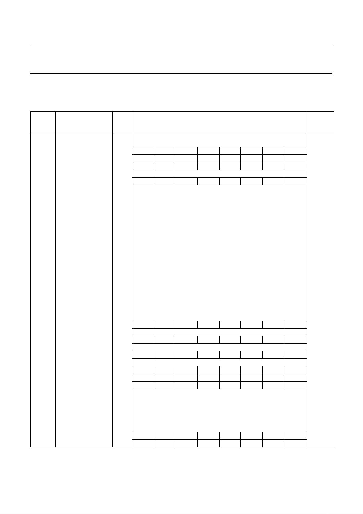
Table 10 CAN Special Function Registers
SFR ACCESS
PELICAN
REG.
BIT7 BIT6 BIT5 BIT4 BIT3 BIT2 BIT1 BIT0
SFR
ADDR
CANADR Read/
Write
- CANA7 CANA6 CANA5 CANA4 CANA3 CANA2 CANA1 CANA0 C1
CANDAT Read/
Write
- CAND7 CAND6 CAND5 CAND4 CAND3 CAND2 CAND1 CAND0 C2
CANMOD Read/
Write
Mode TM RIPM RPM SM − STM LOM RM C4
CANSTA Read Status BS ES TS RS TCS TBS DOS RBS C0
Write Interrupt
Enable
BEIE ALIE EPIE WUIE DOIE EIE TIE RIE
CANCON Read Interrupt BEI ALI EPI WUI DOI EI TI RI C3
Write Command - - - SRR CDO RRB AT TR
12.3.2 CANADR
This read/write register defines the address of one of the
PeliCAN internal registers to be accessed via CANDAT. It
could be interpreted as a pointer to the PeliCAN.
The read and write access to the PeliCAN Block register is
performed using the CANDAT register.
With the implemented auto address increment mode a fast
stack-like reading and writing of CAN Controller internal
registers is provided. IF the currently defined address
within CANADR is above or equal to 32 decimal, the
content of CANADR is incremented automatically after any
read or write access to CANDAT. For instance, loading a
message into the Transmit Buffer can be done by writing
the first Transmit Buffer Address (112 decimal) into
CANADR and then moving byte by byte of the message to
CANDAT. Incrementing CANADR beyond FFh resets
CANADR to 00h.
In case CANADR is below 32 decimal, there is no
automatic address incrementation performed. CANADR
keeps its value even if CANDAT is accessed for reading or
writing. This is to allow polling of registers in the lower
address space of the PeliCAN Controller.
12.3.3 CANDAT REGISTER
CANDAT is implemented as a read/write register.
The Special Function Register CANDAT appears as a port
to the CAN Controller’s internal register (memory location)
being selected by CANADR. Reading or writing CANDAT
is effectively an access to that PeliCAN internal register,
which is selected by CANADR. CANDAT is implemented
as a read/write register.
Note that any access to this register automatically
increments CANADR if the current address within
CANADR is above ore equal to 32 decimal.
12.3.4 CANMOD
With a read or write access to CANMOD the Mode
Register of the PeliCAN is accessed directly. The Mode
register is located at address 00h within the PeliCAN
Block.
12.3.5 CANSTA
The CANSTA SFR provides a direct access to the Status
Register of the PeliCAN as well as to the Interrupt Enable
Register, depending on the direction of the access.
Reading CANSTA is an access to the Status Register of
the PeliCAN (address 2). When writing to CANSTA the
Interrupt Enable Register is accessed (address 4).
12.3.6 CANCON
The CANCON SFR provides a direct access to the
Interrupt Register of the PeliCAN as well as to the
Command register, depending on the direction of the
access.
When reading CANCON the Interrupt Register of the
PeliCAN is accessed (address 3), while writing to
CANCON means an access to the Command Register
(address 01).

1999 Aug 19 29
Philips Semiconductors Objective Specification
Single-chip 8-bit microcontroller with CAN controller P8xC591
12.4 Register and Message Buffer description
12.4.1 ADDRESS LAYOUT
The PeliCAN internal registers appear to the host CPU as on-chip memory mapped peripheral registers. Because the
PeliCAN can operate in different modes (Operating / Reset, see also Mode Register), one have to distinguish between
different internal address definitions. Starting from CAN Address 128 the complete internal FIFO RAM is mapped to the
CPU Interface.
Table 11 Address allocation
CAN
ADDR.
OPERATING MODE RESET MODE
READ WRITE READ WRITE
0 Mode Mode Mode Mode
1 (00) Command (00) Command
2 Status - Status 3 Interrupt - Interrupt 4 Interrupt Enable Interrupt Enable Interrupt Enable Interrupt Enable
5 Rx Interrupt Level Rx Interrupt Level Rx Interrupt Level Rx Interrupt Level
6 Bus Timing 0 - Bus Timing 0 Bus Timing 0
7 Bus Timing 1 - Bus Timing 1 Bus Timing 1
8 See Note 2 - - 9 Rx Message Counter - Rx Message Counter -
10 Rx Buffer Start Address - Rx Buffer Start Address -
11 Arbitration Lost Capture - Arbitration Lost Capture 12 Error Code Capture - Error Code Capture 13 Error Warning Limit Error Warning Limit Error Warning Limit Error Warning Limit
14 Rx Error Counter - Rx Error Counter Rx Error Counter
15 TX Error Counter - TX Error Counter TX Error Counter
16 to 28 reserved (00) - reserved (00) -
29 ACF Mode - ACF Mode ACF Mode
30 ACF Enable ACF Enable ACF Enable ACF Enable
31 ACF Priority ACF Priority ACF Priority ACF Priority
32
B
A
N
K
1
Acceptance Code 0 Acceptance Code 0 Acceptance Code 0 Acceptance Code 0
33 Acceptance Code 1 Acceptance Code 1 Acceptance Code 1 Acceptance Code 1
34 Acceptance Code 2 Acceptance Code 2 Acceptance Code 2 Acceptance Code 2
35 Acceptance Code 3 Acceptance Code 3 Acceptance Code 3 Acceptance Code 3
36 Acceptance Mask 0 Acceptance Mask 0 Acceptance Mask 0 Acceptance Mask 0
37 Acceptance Mask 1 Acceptance Mask 1 Acceptance Mask 1 Acceptance Mask 1
38 Acceptance Mask 2 Acceptance Mask 2 Acceptance Mask 2 Acceptance Mask 2
39 Acceptance Mask 3 Acceptance Mask 3 Acceptance Mask 3 Acceptance Mask 3
40
B
A
N
K
2
Acceptance Code 0 Acceptance Code 0 Acceptance Code 0 Acceptance Code 0
41 Acceptance Code 1 Acceptance Code 1 Acceptance Code 1 Acceptance Code 1
42 Acceptance Code 2 Acceptance Code 2 Acceptance Code 2 Acceptance Code 2
43 Acceptance Code 3 Acceptance Code 3 Acceptance Code 3 Acceptance Code 3
44 Acceptance Mask 0 Acceptance Mask 0 Acceptance Mask 0 Acceptance Mask 0
45 Acceptance Mask 1 Acceptance Mask 1 Acceptance Mask 1 Acceptance Mask 1
46 Acceptance Mask 2 Acceptance Mask 2 Acceptance Mask 2 Acceptance Mask 2
47 Acceptance Mask 3 Acceptance Mask 3 Acceptance Mask 3 Acceptance Mask 3

1999 Aug 19 30
Philips Semiconductors Objective Specification
Single-chip 8-bit microcontroller with CAN controller P8xC591
48
B
A
N
K
3
Acceptance Code 0 Acceptance Code 0 Acceptance Code 0 Acceptance Code 0
49 Acceptance Code 1 Acceptance Code 1 Acceptance Code 1 Acceptance Code 1
50 Acceptance Code 2 Acceptance Code 2 Acceptance Code 2 Acceptance Code 2
51 Acceptance Code 3 Acceptance Code 3 Acceptance Code 3 Acceptance Code 3
52 Acceptance Mask 0 Acceptance Mask 0 Acceptance Mask 0 Acceptance Mask 0
53 Acceptance Mask 1 Acceptance Mask 1 Acceptance Mask 1 Acceptance Mask 1
54 Acceptance Mask 2 Acceptance Mask 2 Acceptance Mask 2 Acceptance Mask 2
55 Acceptance Mask 3 Acceptance Mask 3 Acceptance Mask 3 Acceptance Mask 3
56
B
A
N
K
4
Acceptance Code 0 Acceptance Code 0 Acceptance Code 0 Acceptance Code 0
57 Acceptance Code 1 Acceptance Code 1 Acceptance Code 1 Acceptance Code 1
58 Acceptance Code 2 Acceptance Code 2 Acceptance Code 2 Acceptance Code 2
59 Acceptance Code 3 Acceptance Code 3 Acceptance Code 3 Acceptance Code 3
60 Acceptance Mask 0 Acceptance Mask 0 Acceptance Mask 0 Acceptance Mask 0
61 Acceptance Mask 1 Acceptance Mask 1 Acceptance Mask 1 Acceptance Mask 1
62 Acceptance Mask 2 Acceptance Mask 2 Acceptance Mask 2 Acceptance Mask 2
63 Acceptance Mask 3 Acceptance Mask 3 Acceptance Mask 3 Acceptance Mask 3
64 to 95 reserved (00) - reserved (00) -
(SFF) (EFF) (SFF) (EFF) (SFF) (EFF)
96 Rx Frame Info Rx Frame Info - Rx Frame Info Rx Frame Info Rx Frame Info Rx Frame Info
97 Rx Identifier 1 Rx Identifier 1 - Rx Identifier 1 Rx Identifier 1 Rx Identifier 1 Rx Identifier 1
98 Rx Identifier 2 Rx Identifier 2 - Rx Identifier 2 Rx Identifier 2 Rx Identifier 2 Rx Identifier 2
99 Rx Data 1 Rx Identifier 3 - Rx Data 1 Rx Identifier 3 Rx Data 1 Rx Identifier 3
100 Rx Data 2 Rx Identifier 4 - Rx Data 2 Rx Identifier 4 Rx Data 2 Rx Identifier 4
101 Rx Data 3 Rx Data 1 - Rx Data 3 Rx Data 1 Rx Data 3 Rx Data 1
102 Rx Data 4 Rx Data 2 - Rx Data 4 Rx Data 2 Rx Data 4 Rx Data 2
103 Rx Data 5 Rx Data 3 - Rx Data 5 Rx Data 3 Rx Data 5 Rx Data 3
104 Rx Data 6 Rx Data 4 - Rx Data 6 Rx Data 4 Rx Data 6 Rx Data 4
105 Rx Data 7 Rx Data 5 - Rx Data 7 Rx Data 5 Rx Data 7 Rx Data 5
106 Rx Data 8 Rx Data 6 - Rx Data 8 Rx Data 6 Rx Data 8 Rx Data 6
107 (FIFO RAM)
(1)
Rx Data 7 - (FIFO RAM)
(1)
Rx Data 7 (FIFO RAM)
(1)
Rx Data 7
108 (FIFO RAM)
(1)
Rx Data 8 - (FIFO RAM)
(1)
Rx Data 8 (FIFO RAM)
(1)
Rx Data 8
109 to 111 reserved (00) - reserved (00) -
(SFF) (EFF) (SFF) (EFF) (SFF) (EFF)
112 Tx Frame Info Tx Frame Info Tx Frame Info Tx Frame Info Tx Frame Info Tx Frame Info Tx Frame Info Tx Frame Info
113 Tx Identifier 1 Tx Identifier 1 Tx Identifier 1 Tx Identifier 1 Tx Identifier 1 Tx Identifier 1 Tx Identifier 1 Tx Identifier 1
114 Tx Identifier 2 Tx Identifier 2 Tx Identifier 2 Tx Identifier 2 Tx Identifier 2 Tx Identifier 2 Tx Identifier 2 Tx Identifier 2
CAN
ADDR.
OPERATING MODE RESET MODE
READ WRITE READ WRITE
 Loading...