

Philips P83C557E6,P80C557E6 Datasheet

P83C557E6/P80C557E6
Single-chip 8-bit microcontroller
Product specification 1999 Mar 02
INTEGRATED CIRCUITS

Philips Semiconductors Product specification
P83C557E6/P80C557E6Single-chip 8-bit microcontroller
2
1999 Mar 02
1. FEATURES
•80C51 central processing unit
•48 K × 8 ROM, expandable externally to 64 Kbytes
•ROM Code protection
•1536 × 8 RAM, expandable externally to 64 Kbytes
•Two standard 16-bit timer/counters
•An additional 16-bit timer/counter coupled to four capture registers
and three compare registers
•A 10-bit ADC with eight multiplexed analog inputs and
programmable autoscan
•Two 8-bit resolution, pulse width modulation outputs
•Five 8-bit I/O ports plus one 8-bit input port shared with analog
inputs
•I
2
C-bus serial I/O port with byte oriented master and slave
functions
•Full-duplex UART compatible with the standard 80C51
•On-chip watchdog timer
•15 interrupt sources with 2 priority levels (2 to 6 external sources
possible)
•Extended temperature range (–40 to +85 °C)
•4.5 to 5.5 V supply voltage range
•Frequency range for 80C51–family standard oscillator: 3.5 MHz to
16 MHz
•PLL oscillator with 32 kHz reference and software–selectable
system clock frequency
•Seconds Timer
•Software enable/disable of ALE output pulse
•Electromagnetic compatibility improvements
•Wake–up from Power–down by external or seconds interrupt
2. GENERAL DESCRIPTION
The P80C557E6/P83C557E6 (hereafter generically referred to as
P8xC557E6) single-chip 8-bit microcontroller is manufactured in an
advanced CMOS process and is a derivative of the 80C51
microcontroller family . The P8xC557E6 has the same instruction set
as the 80C51. Three versions of the derivative exist:
•P83C557E6 — 48 Kbytes mask programmable ROM
•P80C557E6 — ROMless version of the P83C557E6
The P8xC557E6 contains a non-volatile 48 Kbytes mask
programmable ROM (P83C557E6), a volatile 1536 × 8 read/write
data memory, five 8-bit I/O ports, one 8-bit input port, two 16-bit
timer/event counters (identical to the timers of the 80C51), an
additional 16-bit timer coupled to capture and compare latches, a
15-source, two-priority-level, nested interrupt structure, an 8-input
ADC, a dual DAC pulse width modulated interface, two serial
interfaces (UART and I
2
C-bus), a “watchdog” timer, an on-chip
oscillator and timing circuits. For systems that require extra
capability the P8xC557E6 can be expanded using standard TTL
compatible memories and logic.
In addition, the P8xC557E6 has two software selectable modes of
power reduction — Idle Mode and power-down mode. The Idle
Mode freezes the CPU while allowing the RAM, timers, serial ports,
and interrupt system to continue functioning. The power-down mode
saves the RAM contents but freezes the oscillator, causing all other
chip functions to be inoperative.
The device also functions as an arithmetic processor having
facilities for both binary and BCD arithmetic as well as bit-handling
capabilities. The instruction set consists of over 100 instructions: 49
one-byte, 45 two-byte, and 17 three- byte. With a 16 MHz system
clock, 58% of the instructions are executed in 0.75 µs and 40% in
1.5 µs. Multiply and divide instructions require 3 µs.

Philips Semiconductors Product specification
P83C557E6/P80C557E6Single-chip 8-bit microcontroller
1999 Mar 02
3
3. ORDERING INFORMATION
PACKAGE
FREQUENCY TEMPERATURE
EXTENDED TYPE NUMBER
NAME DESCRIPTION CODE
RANGE (MHz) RANGE (°C)
ROMless
P80C557E6EBB QFP80 Plastic Quad Flat Pack; 80 leads SOT318-1 3.5 to 16 0 to +70
P80C557E6EFB QFP80 Plastic Quad Flat Pack; 80 leads SOT318-1 3.5 to 16 –40 to +85
ROM coded
P83C557E6EBB/YYY
1
QFP80 Plastic Quad Flat Pack; 80 leads SOT318-1 3.5 to 16 0 to +70
P83C557E6EFB/YYY
1
QFP80 Plastic Quad Flat Pack; 80 leads SOT318-1 3.5 to 16 –40 to +85
NOTE:
1. YYY denotes the ROM code number.
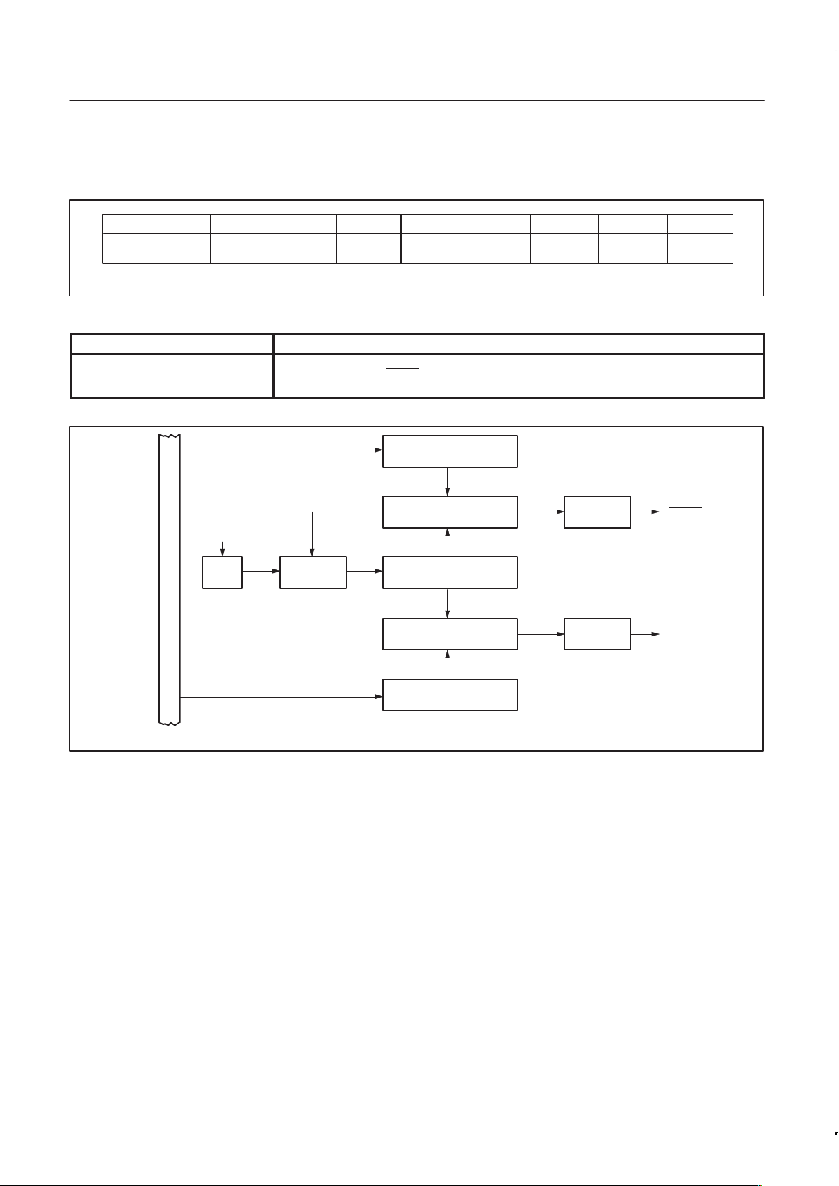
CPU
ADC
8-BIT INTERNAL BUS
P0 P1 P2 P3 TxD RxD P5 P4 CT0I-CT3I T2 RT2
CMSR0-CMSR5
CMT0, CMT1
RSTOUT
EW
XTAL1
XTAL2
EA
ALE
PSEN
WR
RD
T0 T1 INT0 INT1
V
DD
V
SS
PWM0 PWM1
AV
SS
AV
DD
AV
REF
–
+
ADEXS
ADC0-7 SDA SCL
3 3 3 3
3 3
0
2
1 1 1 4
5
0
1
2
ALTERNATE FUNCTION OF PORT0
3
4
5
AD0-7
A8-15
3
3
16
T0, T1
TWO 16-BIT
TIMER/EVENT
COUNTERS
PROGRAM
MEMORY
48 K x 8 ROM
DATA
MEMORY
256 x 8 RAM
+
1280 x 8 RAM
DUAL
PWM
I
2
C
SERIAL
I/O
80C51 CORE
EXCLUDING
ROM/RAM
PARALLEL I/O
PORTS AND
EXTERNAL BUS
SERIAL
UART
PORT
8-BIT
PORTS
FOUR
16-BIT
CAPTURE
LATCHES
T2
16-BIT
TIMER/
EVENT
COUNT-
ERS
T2
16-BIT
COMPARA-
TORS
WITH
REGISTERS
COMPARA-
TOR
OUTPUT
SELECTION
T3
WATCH–
DOG
TIMER
ALTERNATE FUNCTION OF PORT1
ALTERNATE FUNCTION OF PORT2
ALTERNATE FUNCTION OF PORT 3
ALTERNATE FUNCTION OF PORT 4
ALTERNATE FUNCTION OF PORT 5
Figure 1. Block diagram P8xC557E6.
6
NOT PRESENT IN P80C557E6
6
PLL
oscillator
+
”seconds”
timer
XTAL3 XTAL4
SELXTAL1
RSTIN
16
Philips Semiconductors Product specification
P83C557E6/P80C557E6Single-chip 8-bit microcontroller
1999 Mar 02
4
PORT 5
PORT 4
ADC0-7
CMT0
CMT1
CMSR0-5
RSTOUT
EW
XTAL1
XTAL2
EA
ALE/WE
PSEN
AVref+
AVref–
ADEXS
PWM0
PWM1
PORT 0
LOW ORDER
ADDRESS AND
DATA BUS
PORT 1PORT 2PORT 3
CT0I/INT2
CT1I/INT3
CT2I/INT4
CT3I/INT5
T2
RT2
RxD/DATA
TxD/CLOCK
INT0
INT1
T0
T1
WR
RD
V
SS
V
DD
AV
SS
AV
DD
HIGH ORDER
ADDRESS BUS
P8xC557E6
Figure 2. Functional diagram.
SCL
SDA
A8–15
AD0–7
RSTIN
XTAL3
XTAL4
SELXTAL1
0
1
2
3
4
5
6
7
0
1
2
3
4
5
6
7
0
1
2
3
4
5
6
7
0
1
2
3
4
5
6
7
0
1
2
3
4
5
6
7
0
1
2
3
4
5
6
7
0
1
2
3
4
5
6
7

Philips Semiconductors Product specification
P83C557E6/P80C557E6Single-chip 8-bit microcontroller
1999 Mar 02
5
4. PINNING
Figure 3. Pinning diagram for QFP80 (SOT318).
1
2
3
4
5
6
7
8
9
10
11
12
13
14
15
16
17
18
19
20
21
22
23
24
64
63
62
61
60
59
58
57
56
55
54
53
52
51
50
49
48
47
46
45
44
43
42
41
25
26
27
32
33
34
35
36
37
38
39
40
80
79
78
77
76
75
74
73
72
71
70
69
68
67
66
65
P8xC557E6
AV
ref–
AV
ref+
AV
SS
1
AV
DD1
P5.7/ADC7
P5.6/ADC6
P5.5/ADC5
P5.4/ADC4
P5.3/ADC3
P5.2/ADC2
P5.1/ADC1
P5.0/ADC0
V
SS1
V
DD1
ADEXS
PWM0
PWM1
EW
P4.0/CMSR0
P4.1/CMSR1
P4.2/CMSR2
P4.3/CMSR3
RSTOUT
P4.4/CSMR4
P4.5/CMSR5
P4.6/CMT0
P4.7/CMT1
DD2VSS2
V
RSTIN
P1.0/CT0I/INT2
P1.1/CT1I/INT3
P1.2/CT2I/INT4
P1.3/CT3I/INT5
P1.4/T2
P1.5/RT2
P1.6
P1.7
SCL
SDA
P3.0/RXD
ALE/WE
PSEN
P2.5/A13
P2.4/A12
P2.3/A11
P2.2/A10
P2.1/A9
P2.0/A8
V
SS3
V
DD3
n.c.
n.c.
P3.6/WR
P3.5/T1
P3.4/T0
P3.3/INT1
P3.2/INT0
P3.1/TXD
SELXTAL1
XTAL4
XTAL3
SS4VDD4
V
P0.0/AD0
P0.1/AD1
P0.2/AD2
P0.3/AD3
P0.4/AD4
P0.5/AD5
P0.6/AD6
P0.7/AD7
EA
P3.7/RD
XTAL2
XTAL1
P2.6/A14
P2.7/A15
DD2
AV
SS2
AV
28
29
30
31
n.c. = not connected

Philips Semiconductors Product specification
P83C557E6/P80C557E6Single-chip 8-bit microcontroller
1999 Mar 02
6
4.1 PIN DESCRIPTIONS
SYMBOL PIN DESCRIPTION
AV
ref–
AV
ref+
1
2
Low end of analog to digital conversion reference resistor
High end of analog to digital conversion reference resistor.
AV
SS1
AV
DD1
3
4
Analog ground for ADC
Analog power supply (+5 V) for ADC
AV
SS2
AV
DD2
77
76
Analog ground; for PLL oscillator
Analog power supply; (+5 V) for PLL oscillator
P5.7 – P5.0 5 – 12
Port 5
8–bit input port
Port pin Alternative function
P5.0–P5.7 Eight input channels to ADC (ADC0–ADC7)
V
DD1
, V
DD2
,
V
DD3
, V
DD4
14, 28,
53, 66
Digital power supply: +5 V power supply pins during normal operation and power reduction modes. All pins
must be connected.
V
SS1
, V
SS2
V
SS3
, V
SS4
13, 29,
54, 67
Digital ground: circuit ground potential. All pins must be connected.
ADEXS 15 Start ADC operation: Input starting analog to digital conversion triggered by a programmable edge (ADC
operation can also be started by software). This pin must not float
PWM0 16 Pulse width modulation output 0
PWM1 17 Pulse width modulation output 1
EW 18 Enable watchdog timer: Enable for T3 watchdog timer and disable Power–down Mode.This pin must not
float.
P4.0 – P4.7 19 – 22
24 – 27
Port 4
8–bit quasi–bidirectional I/O port
Port pin Alternative function
P4.0 CMSR0 }
P4.1 CMSR1 }
P4.2 CMSR2 } compare and set/reset
P4.3 CMSR3 } outputs on a match with timer T2
P4.4 CMSR4 }
P4.5 CMSR5 }
P4.6 CMT0 } compare and toggle outputs
P4.7 CMT1 } on a match with timer T2
RSTIN 30 Reset: Input to reset the P8xC557E6.
RSTOUT 23 Reset: Output of the P8xC557E6 for resetting peripheral devices during initialization and Watchdog Timer
overflow.
P1.0 – P1.7 31 – 38 Port 1
8–bit quasi–bidirectional I/O port
Port pin Alternative function
P1.0 CT0I/INT2}
P1.1 CT1I/INT3} : Capture timer inputs for
P1.2 CT2I/INT4} timer T2 or external interrupt inputs
P1.3 CT3I/INT5}
P1.4 T2 : T2 event input, rising edge triggered
P1.5 RT2 : T2 timer reset input, rising edge triggered
P1.6
P1.7
SCL 39 I2C–bus serial clock I/O port
SDA 40 I2C–bus serial data I/O port
If SCL and SDA are not used, they must be connected to V
SS
.

Philips Semiconductors Product specification
P83C557E6/P80C557E6Single-chip 8-bit microcontroller
1999 Mar 02
7
SYMBOL DESCRIPTIONPIN
P3.0 – P3.7 41 – 48 8–bit quasi–bidirectional I/O port
Port pin Alternative function
P3.0 RXD : Serial input port
P3.1 TXD : Serial output port
P3.2 INT0
: External interrupt
P3.3 INT1
: External interrupt
P3.4 T0 : Timer 0 external input
P3.5 T1 : Timer 1 external input
P3.6 WR
: External data memory write strobe
P3.7 RD
: External data memory read strobe
N.C. 49 – 50 Not connected pins.
XTAL2 51 Crystal pin 2: output of the inverting amplifier that forms the oscillator. Left open–circuit when an external oscillator
clock is used.
XTAL1 52 Crystal pin 1: input to the inverting amplifier that forms the oscillator, and input to the internal clock generator.
Receives the external oscillator clock signal when an external oscillator is used. Must be connected to logic
HIGH if the PLL oscillator is selected (SELXTAL1 = LOW)
P2.0 – P2.7 55 – 62 Port2: 8–bit quasi–bidirectional I/O port with internal pull–ups.During access to external memories (RAM/ROM)
that use 16–bit addresses (MOVX@DPTR) Port 2 emits the high order address byte.
Port 2 can sink/source one TTL (=4 LSTTL) input. It can drive CMOS inputs without external pull–ups.
PSEN 63 Program Store Enable output: read strobe to the external program memory via Port 0 and 2. Is activated twice
each machine cycle during fetches from external program memory. When executing out of external program
memory two activations of PSEN
are skipped during each access to external data memory. PSEN is not activated
(remains HIGH) during no fetches from external program memory. PSEN
can sink/source 8 LSTTL inputs. It can
drive CMOS inputs without external pull–ups.
ALE/WE 64 Address Latch Enable output: latches the low byte of the address during access of external memory in normal
operation. It is activated every six oscillator periods except during an external data memory access. ALE/WE
can
sink/–source 8 LSTTL inputs.
It can drive CMOS inputs without an external pull–up.
T o prohibit the toggling of ALE pin (RFI noise reduction) the bit RFI in the PCON Register (PCON.5) must be set
by software. This bit is cleared on RESET and can be set and cleared by software. When set, ALE pin will be pulled
down internally , switching an external address latch to a quiet state. The MOVX instruction will still toggle ALE if
external memory is accessed.
ALE will retain its normal high value during Idle Mode and a low value during Power–down Mode while in the “RFI”
mode. Additionally during internal access (EA = 1) ALE will toggle normally when the address exceeds the internal
program memory size. During external access (EA
= 0) ALE will always toggle normally, whether the flag “RFI”
is set or not.
EA 65 External Access Input: If, during RESET, EA is held at a TTL level HIGH the CPU executes out of the
internal program memory, provided the program counter is less than 49152. If, during RESET, EA
is held at a
TTL level LOW the CPU executes out of external program memory via Port 0 and Port 2. EA
is not allowed to
float. EA
is latched during RESET and don’t care after RESET.
P0.7–P0.0 68 –75 Port 0: 8–bit open drain bidirectional I/O port. It is also the multiplexed low–order address and data bus during
accesses to external memory (during theses accesses internal pull–ups are activated). Port 0 can sink/source 8
LSTTL inputs.
XTAL3 78 Crystal pin, output of the inverting amplifier that forms the 32 kHz oscillator
XTAL4 79 Crystal pin, input to the inverting amplifier that forms the 32 kHz oscillator. XTAL3 and XTAL4 are pulled LOW
if the PLL oscillator is not selected (SELXTAL1 = HIGH) or if Reset is active.
SELXTAL1 80 Must be connected to logic HIGH level to select the HF oscillator, using the XT AL1/XT AL2 crystal. If pulled low the
PLL is selected for clocking of the controller, using the XTAL3/ XTAL4 crystal.
NOTE:
1. To avoid a ‘latch–up’ effect at Power–on, the voltage at any pin at any time must not be higher or lower than V
DD
+ 0.5 V or VSS– 0.5 V
respectively.

Philips Semiconductors Product specification
P83C557E6/P80C557E6Single-chip 8-bit microcontroller
1999 Mar 02
8
5. ELECTROMAGNETICS COMPATIBILITY (EMC)
IMPROVEMENTS
Primary attention was paid on the reduction of electromagnetic
emission of the microcontroller P8xC557E6.
The following features effect in reducing the electromag– netic
emission and additionally improve the electromagnetic susceptibility:
•Four supply voltage pins (V
DD
) and four ground pins (VSS) with
pairs of V
DD
and VSS at two adjacent pins at each side of the
package.
•Separated V
DD
pins for the internal logic and the port buffers
•Internal decoupling capacitance improves the EMC radiation
behavior and the EMC immunity
•External capacitors are to be located as close as possible
between pins V
DD1
and V
SS1,
V
DD2
and V
SS2,
V
DD3
and V
SS3
as
well as V
DD4
and V
SS4
; ceramic chip capacitors are
recommended (100nF).
•The ALE output signal (pulses at a frequency off
CLK
/6) can be
disabled under software control (bit 5 in the SFR PCON: “RFI”); if
disabled, no ALE pulse will occur. ALE pin will be pulled down
internally , switching an external address latch to a quiet state. The
MOVX instruction will still toggle ALE (external data memory is
accessed). ALE will retain its normal HIGH value during Idle Mode
and a LOW value during Power-down mode while in the “RFI”
reduction mode. Additionally during internal access (EA
= 1) ALE
will toggle normally when the address exceeds the internal
program memory size. During external access (EA
= 0) ALE will
always toggle normally , whether the flag “RFI” is set or not.
6. FUNCTIONAL DESCRIPTION
6.1 General
The P8xC557E6 is a stand–alone high–performance microcontroller
designed for use in real time applications such as instrumentation,
industrial control, medium to high–end consumer applications and
specific automotive control applications.
In addition to the 80C51 standard functions, the device provides a
number of dedicated hardware functions for these applications.
The P8xC557E6 is a control–oriented CPU with on–chip program
and data memory. It can be extended with external program memory
up to 64 Kbytes. It can also access up to 64 Kbytes of external data
memory. For systems requiring extra capability, the P8xC557E6 can
be expanded using standard memories and peripherals.
The P8xC557E6 has two software selectable modes of reduced
activity for further power reduction – Idle and Power–down. The Idle
Mode freezes the CPU while allowing the RAM, timers, serial ports
and interrupt system to continue functioning. The Power–down
Mode saves the RAM contents but freezes the oscillator causing all
other chip functions to be inoperative.The Power–down Mode can
be terminated by an external Reset, by the seconds interrupt and by
any one of the two external interrupts. (see description Wake–up
from Power–down Mode).
Program Memory
64 K
DIRECT AND
INDIRECT
Internal
Data Memory
External
64 K
Internal
(EA
= 1)
External
(EA = 0)
255
127
0
Special
Function
Registers
Overlapped
Space
0
External
Data Memory
49152
49151
0
INDIRECT
ONLY
0
49151
1280
(ARD = 1)
(ARD = 0)
AUXILIARY
RAM
Figure 4. Memory map & address space.
1280 bytes

Philips Semiconductors Product specification
P83C557E6/P80C557E6Single-chip 8-bit microcontroller
1999 Mar 02
9
6.2 Memory Organization
The central processing unit (CPU) manipulates operands in three
memory spaces; these are the 64 Kbytes external data memory,
1536 bytes internal data memory (consisting of 256 bytes standard
RAM and 1280 bytes AUX–RAM) and the 48 Kbytes internal and/or
64 Kbytes external program memory (see Figure 4).
6.2.1 Program Memory
The program memory of the P8xC557E6 consists of 48 Kbytes
ROM on–chip, externally expandable up to 64 Kbytes. If, during
RESET, the EA
pin was held HIGH, the P8xC557E6 executes out of
the internal program memory unless the address exceeds 0BFFFH.
Locations 0C000H through 0FFFFH are then fetched from the
external program memory. If the EA
pin was held LOW during
RESET the P8xC557E6 fetches all instructions from the external
program memory. The EA
input is latched during RESET and is
don’t care after RESET.
The internal program memory content is protected, by setting a
mask programmable security bit (ROM), i.e., it cannot be read out at
any time by any test mode or by any instruction in the external
program memory space. The MOVC instructions are the only ones
which have access to program code in the internal or external
program memory. The EA
input is latched during RESET and is
‘don’t care’ after RESET. This implementation prevents from reading
internal program code by switching from external program memory
to internal program memory during MOVC instruction or an
instruction that handles immediate data. Table 1 lists the access to
the internal and external program memory with MOVC instructions
when the security feature has been activated.
6.2.2 Internal Data Memory
The internal data memory is divided into three physically separated
parts:
256 bytes of RAM, 1280 bytes of AUX–RAM, and a 128 bytes
special function area. These can be addressed each in a different
way (see also Table 2).
– RAM 0 to 127 can be addressed directly and indirectly as in the
80C51.
Address pointers are R0 and R1 of the selected registerbank.
– RAM 128 to 255 can only be addressed indirectly.
Address pointers are R0 and R1 of the selected registerbank.
– AUX–RAM 0 to 1279 is also indirectly addressable as external
DATA MEMORY locations 0 to 1279 via MOVX–Datapointer
instruction, unless it is disabled by setting ARD = 1.
AUX–RAM 0 to 1279 is indirectly addressable via pageregister
(XRAMP) and MOVX–Ri instructions, unless it is disabled by
setting ARD = 1 (see Figure 5).
When executing from internal program memory, an access to
AUX–RAM 0 to 1279 will not affect the ports P0, P2, P3.6 and
P3.7.
An access to external DATA MEMORY locations higher than 1279
will be performed with the MOVX @ DPTR instructions in the
same way as in the 80C51 structure, so with P0 and P2 as
data/address bus and P3.6 and P3.7 as write and read timing
signals. Note that the external DATA MEMORY cannot be
accessed with R0 and R1 as address pointer if the AUX–RAM is
enabled (ARD = 0, default).
– The Special Function Registers (SFR) can only be addressed
directly in the address range from 128 to 255 (see Table 5).
– Four register banks, each 8 registers wide, occupy locations 0
through 31 in the lower RAM area. Only one of these banks may
be enabled at a time. The next 16 bytes, locations 32 through 47,
contain 128 directly addressable bit locations.The stack can be
located anywhere in the internal 256 bytes RAM.The stack depth
is only limited by the available internal RAM space of 256 bytes
(see Figure 7).
All registers except the program counter and the four register
banks reside in the Special Function Register address space.
Table 1. Memory access by the MOVC instruction for protected ROMs
MOVC LOCATION ACCESS TO INTERNAL
PROGRAM MEMORY
ACCESS TO EXTERNAL
PROGRAM MEMORY
MOVC in internal program memory YES YES
MOVC in external program memory NO YES
NOTE:
1. If the security feature has not been activated, there are no restrictions for MOVC instructions.
T able 2. Internal data memory map
LOCATION ADDRESSED
RAM 0 to 127 Direct and indirect
AUX–RAM 0 to 1279 Indirect only with MOVX
RAM 128 to 255 Indirect only
SFR 128 to 255 Direct only
Philips Semiconductors Product specification
P83C557E6/P80C557E6Single-chip 8-bit microcontroller
1999 Mar 02
10
MOVX @DPTR,A
MOVX A,@DPTR
MOVX A, @Ri
MOVX @Ri, A
255
255
0
255
0
0
767
(XRAMP) = 02 H
(XRAMP) = 01 H
(XRAMP) = 00 H
0
Figure 5. Indirect addressing of AUX–RAM (1280 Bytes), ARD bit in PCON = 0.
512
511
256
255
(XRAMP) = 03 H
(XRAMP) = 04 H
1024
1023
768
1279
0
255
0
255

Philips Semiconductors Product specification
P83C557E6/P80C557E6Single-chip 8-bit microcontroller
1999 Mar 02
11
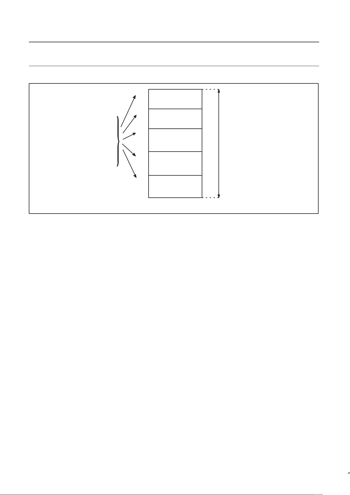
6.2.2.1 AUX–RAM Page Register XRAMP
The AUX–RAM Page Register is used to select one of five 256
bytes pages of the internal 1280 bytes AUX–RAM for
MOVX–accesses via R0 or R1. Its reset value is (XXXXX000).
7 6 5 4 3 2 1 0
x x x x x XRAMP2 XRAMP1 XRAMP0
XRAMP (FAH)
Figure 6. AUX–RAM page register.
x: undefined during read, a write operation must write “0” to these locations
Table 3. Description of XRAMP bits
BIT SYMBOL FUNCTION
XRAMP.3–7 XRAMPx reserved for future use
XRAMP.2 XRAMP2 AUX–RAM page select bit 2
XRAMP.1 XRAMP1 AUX–RAM page select bit 1
XRAMP.0 XRAMP0 AUX–RAM page select bit 0
Table 4. Memory locations for all possible MOVX–accesses
ARD
1
XRAMP2 XRAMP1 XRAMP0 MOVX @Ri,A and MOVX A,@Ri instructions access:
0 0 0 0 AUX–RAM locations 0 .. 255 (reset condition)
0 0 0 1 AUX–RAM locations 256 .. 511
0 0 1 0 AUX–RAM locations 512 .. 767
0 0 1 1 AUX–RAM locations 768 ... 1023
0 1 0 0 AUX–RAM locations 1024 .. 1279
0 1 0 1 no valid memory access; reserved for future use
0 1 1 X no valid memory access; reserved for future use
1 X X X External RAM locations 0 .. 255
MOVX @DPTR,A and MOVX A,@DPTR instructions access:
0 X X X AUX–RAM locations 0 .. 1279 (reset condition)
External RAM locations 1280 .. 65535
1 X X X External RAM locations 0 .. 65535
NOTE:
1. ARD (AUX–RAM Disable) is a bit in the Special Function Register PCON

Philips Semiconductors Product specification
P83C557E6/P80C557E6Single-chip 8-bit microcontroller
1999 Mar 02
12
Table 5. Special Function Register Memory Map and Reset Values
High Nibble of SFR Address
LOW 8 9 A B C D E F
0 P0 %
11111111
P1 %
11111111
P2 %
11111111
P3 %
11111111
P4 %
11111111
PSW %
00000000
ACC %
00000000
B %
00000000
1 SP 00000111
2 DPL
00000000
3 DPH
00000000
4
5
6 ADRSL0 #
XXXXXXXX
ADRSL1 #
XXXXXXXX
ADRSL2 #
XXXXXXXX
ADRSL3 #
XXXXXXXX
ADRSL4 #
XXXXXXXX
ADRSL5 #
XXXXXXXX
ADRSL6 #
XXXXXXXX
ADRSL7 #
XXXXXXXX
7 PCON
00000000
P5 #
XXXXXXXX
ADCON
00000000
ADPSS
00000000
ADRSH #
000000XX
8 TCON %
00000000
S0CON %
00000000
IEN0 %
00000000
IP0 %
X0000000
TM2IR %
00000000
S1CON %
00000000
IEN1 %
00000000
IP1 %
00000000
9 TMOD
00000000
S0BUF
XXXXXXXX
CML0
00000000
CMH0
00000000
S1STA #
11111000
PLLCON
00001 101
A TL0
00000000
CML1
00000000
CMH1
00000000
S1DAT
00000000
TM2CON
00000000
XRAMP
XXXXX000
B TL1
00000000
CML2
00000000
CMH2
00000000
S1ADR
00000000
CTCON
00000000
C TH0
00000000
CTL0 #
XXXXXXXX
CTH0 #
XXXXXXXX
TML2 #
00000000
PWM0
00000000
D TH1
00000000
CTL1 #
XXXXXXXX
CTH1 #
XXXXXXXX
TMH2 #
00000000
PWM1
00000000
E CTL2 #
XXXXXXXX
CTH2 #
XXXXXXXX
STE
11000000
PWMP
00000000
F CTL3 #
XXXXXXXX
CTH3 #
XXXXXXXX
RTE
00000000
T3
00000000
% = Bit addressable register
# = Read only register
X = Undefined
6.3 Addressing
The P8xC557E6 has five methods for addressing:
•Register
•Direct
•Register–Indirect
•Immediate
•Base–Register plus Index–Register–Indirect
The first three methods can be used for addressing destination
operands. Most instructions have a “destination/source” field that
specifies the data type, addressing methods and operands involved.
For operations other than MOVs, the destination operand is also a
source operand.
Access to memory addresses is as follows:
•Register in one of the four register banks through Register, Direct
or Register–Indirect addressing
•1536 bytes of internal RAM through Direct or Register–Indirect
addressing. Bytes 0–127 of internal RAM may be addressed
directly/indirectly . Bytes 128–255 of internal RAM share their
address location with the SFRs and so may only be addressed
indirectly as data RAM. Bytes 0–1279 of AUX–RAM can only be
addressed indirectly via MOVX.
•Special Function Register through direct addressing at address
locations 128–255 (see Figure 8).
•External data memory through Register–Indirect addressing
•Program memory look–up tables through Base– Register plus
Index–Register–Indirect addressing

Philips Semiconductors Product specification
P83C557E6/P80C557E6Single-chip 8-bit microcontroller
1999 Mar 02
13
FFH
68696B 6A6C6D6F 6E
78797B 7A7C7D7F 7E
2FH
2DH
2CH
2BH
2AH
29H
28H
27H
26H
23H
21H
20H
1FH
18H
17H
0FH
10H
08H
25H
07H
22H
24H
255
47
45
44
43
42
41
40
39
37
35
33
32
31
24
23
36
15
16
8
7
38
0
707173 72747577 762EH 46
505153 52545557 56
606163 62646567 66
58595B 5A5C5D5F 5E
404143 42444547 46
48494B 4A4C4D4F 4E
28292B 2A2C2D2F 2E
38393B 3A3C3D3F 3E
303133 32343537 36
18191B 1A1C1D1F 1E
202123 22242527 26
000103 02040507 06
101113 12141517 16
08090B 0A0C0D0F 0E
00H
34
Bank 3
Bank 2
Bank 1
Bank 0
(MSB) (LSB)
Figure 7. RAM bit addresses.
BIT ADDRESS (HEX)
BYTE ADDRESS
(HEX)
BYTE ADDRESS
(DECIMAL)

Philips Semiconductors Product specification
P83C557E6/P80C557E6Single-chip 8-bit microcontroller
1999 Mar 02
14
F8H
F0H
E8H
E0H
D8H
D0H
B8H
C0H
A8H
B0H
A0H
98H
90H
80H
IP1
B
IEN1
ACC
PSW
P4
IP0
P3
IEN0
P2
S0CON
P0
P1
TCON
TM2IR
REGISTER
MNEMONIC
BIT ADDRESS (HEX)
DIRECT BYTE
ADDRESS (HEX)
C8H
88H
S1CON
F8F9FB FAFCFDFF FE
F0F1F3 F2F4F5F7 F6
ECT0ECT1ECT3 ECT2ECM0ECM1ET2 ECM2
E8E9EB EAECEDEF EE
E0E1E3 E2E4E5E7 E6
CR0CR1SI AASTOSTACR2 ENS1
D8D9DB DADCDDDF DE
PF1RS0 OVRS1F0CY AC
D0D1D3 D2D4D5D7 D6
CTI0CTI1CTI3 CTI2CMI0CMI1T2OV CMI2
C8C9CB CACCCDCF CE
C0C1C3 C2C4C5C7 C6
PX0PT0PT1 PX1PS0PS1–PAD
B8B9BB BABCBDBF BE
B0B1B3 B2B4B5B7 B6
EX0ET0ET1 EX1ES0ES1EA EAD
A8A9AB AAACADAF AE
A0A1A3 A2A4A5A7 A6
RITITB8 RB8RENSM2
SM0
SM1
98999B 9A9C9D9F 9E
909193 92949597 96
IT0IE0IE1 IT1TR0TF0TF1 TR1
88898B 8A8C8D8F 8E
808183 82848587 86
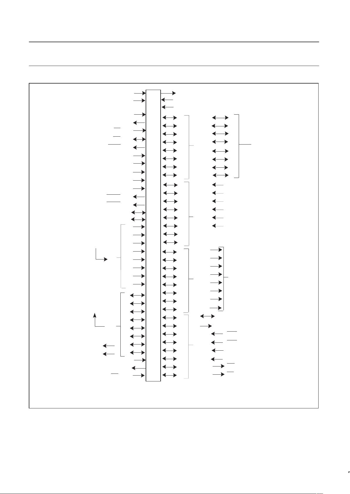
Figure 8. Special Function Register bit addresses.
(MSB) (LSB)FFH
PT2 PCM2 PCM1 PCM0 PCT3 PCT2 PCT1 PCT0
Philips Semiconductors Product specification
P83C557E6/P80C557E6Single-chip 8-bit microcontroller
1999 Mar 02
15
6.4 I/O Facilities
The P8xC557E6 has six 8–bit ports. Ports 0 to 3 are the same as in
the 80C51, with the exception of the additional functions of Port 1.
The parallel I/O function of Port 4 is equal to that of Ports 1, 2 and 3.
Port 5 has a parallel input port function, but has no function as an
output port.
The SDA and SCL lines serve the serial port SI01 (I
2
C). Because
the I
2
C–bus may be active while the device is disconnected from
V
DD,
these pins, are provided with open drain drivers.
Ports 0, 1, 2, 3, 4 and 5 perform the following alternative functions:
Port 0 : provides the multiplexed low–order address and
data bus used for expanding the P8xC557E6 with
standard memories and peripherals.
Port 1 : Port 1 is used for a number of special functions:
4 capture inputs (or external interrupt request inputs
if capture information is not utilized)
– external counter input
– external counter reset input
Port 2 : provides the high–order address bus when the
P8xC557E6 is expanded with external Program
Memory and/or external Data Memory.
Port 3 : pins can be configured individually to provide:
– external interrupt request inputs
– counter inputs
– receiver input and transmitter output of seri port
SIO 0 (UART)
– control signals to read and write external Data
Memory
Port 4 : can be configured to provide signals indicating a
match between timer counter T2 and its compare
registers.
Port 5 : may be used in conjunction with the ADC inter-
face.Unused analog inputs can be used as digital
inputs. As Port 5 lines may be used as inputs to the
ADC, these digital inputs have an inherent hysteresis to prevent the input logic from drawing too much
current from the power lines when driven by analog
signals. Channel to channel crosstalk should be taken into consideration when both digital and analog
signals are simultaneously input to Port 5 (see DC
characteristics).
All ports are bidirectional with the exception of Port 5 which is an
input port.
Pins of which the alternative function is not used may be used as
normal bidirectional I/Os.
The generation or use of a Port 1, Port 3 or Port 4 pin as an
alternative function is carried out automatically by the P8xC557E6
provided the associated Special Function Register bit is set HIGH.
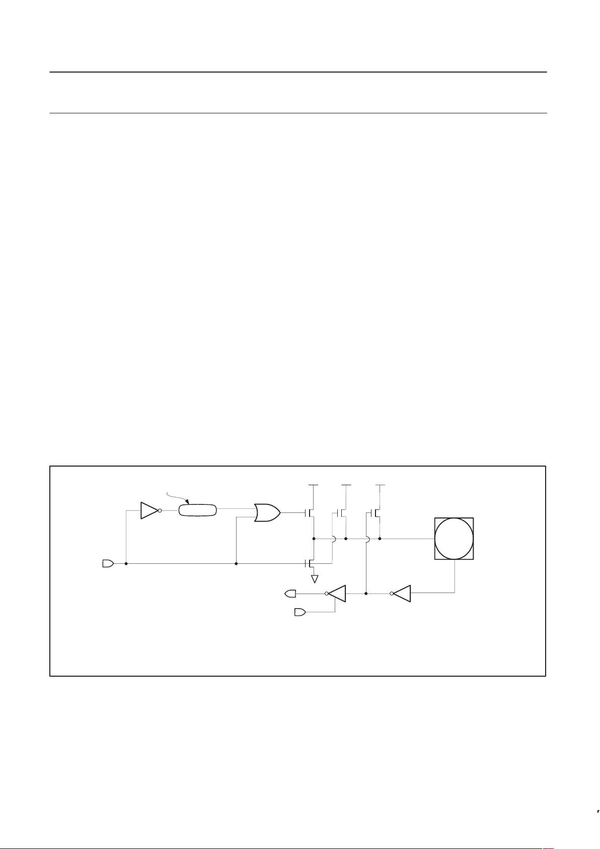
The pull–up arrangements of Ports 1 – 4 are shown in Figure 9.
Figure 9. I/O buffers in the P8xC557E6 (Ports 1, 2, 3 and 4).
V
DD
QN
2 System Clock Periods
Port
Pin
n
From Port
Latch
V
DD
V
DD
P1 P2 P3
Input Data
Read Port Pin
P1 is turned on for 2 system clock periods after QN makes a 1–to–0 transition.
During this time, P1 also turns on P3 through the inverter to form an additional pull up.
Philips Semiconductors Product specification
P83C557E6/P80C557E6Single-chip 8-bit microcontroller
1999 Mar 02
16
6.5 Pulse Width Modulated Outputs
The P8xC557E6 contains two pulse width modulated output
channels (see Figure 13). These channels generate pulses of
programmable length and interval. The repetition frequency is
defined by an 8-bit prescaler PWMP, which supplies the clock for the
counter. The prescaler and counter are common to both PWM
channels. The 8-bit counter counts module 255, i.e., from 0 to 254
inclusive. The value of the 8-bit counter is compared to the contents
of two registers: PWM0 and PWM1. Provided the contents of either
of these registers is greater than the counter value, the
corresponding PWM0
or PWM1 output is set LOW. If the contents of
these registers are equal to, or less than the counter value, the
output will be HIGH. The pulse-width-ratio is therefore defined by the
contents of the registers PWM0 and PWM1. The pulse-width-ratio is
in the range of 0/255 to 255/255 and may be programmed in
increments of 1/255.
Buffered PWM outputs may be used to drive DC motors. The
rotation speed of the motor would be proportional to the contents of
PWMn. The PWM outputs may also be configured as a dual DAC. In
this application, the PWM outputs must be integrated using
conventional operational amplifier circuitry. If the resulting output
voltages have to be accurate, external buffers with their own analog
supply should be used to buffer the PWM outputs before they are
integrated. The repetition frequency fpwm, at the PWMn outputs is
give by:
f
PWM
f
CLK
2 (1 PWMP) 255
This gives a repetition frequency range of 123 Hz to 31.4 kHz
(f
CLK
= 16 MHz). By loading the PWM registers with either 00H or
FFH, the PWM channels will output a constant HIGH or LOW level,
respectively. Since the 8-bit counter counts modulo 255, it can never
actually reach the value of the PWM registers when they are loaded
with FFH.
When a compare register (PWM0 or PWM1) is loaded with a new
value, the associated output is updated immediately. It does not
have to wait until the end of the current counter period. Both PWMn
output pins are driven by push-pull drivers. These pins are not used
for any other purpose.
PWMP (FEH) PWMP.7 PWMP.6 PWMP.5 PWMP.4 PWMP.3 PWMP.2 PWMP.1 PWMP.0
Figure 10. Prescaler frequency control register PWMP.
76543210
Table 6. Description of PWMP bits
BIT FUNCTION
PWMP.0 to 7 Prescaler division factor = (PWMP) + 1
Reading PWMP gives the current reload value. The actual count of the prescaler cannot be read.
PWM0 (FCH) PWM0.7 PWM0.6 PWM0.5 PWM0.4 PWM0.3 PWM0.2 PWM0.1 PWM0.0
Figure 11. Pulse width register PWM0.
76543210
Table 7. Description of PWM0 bits
BIT FUNCTION
PWM0.0 to 7
LOW/HIGH ration of PWM0 signal =
(PWM0)
255 – (PWM0)
Philips Semiconductors Product specification
P83C557E6/P80C557E6Single-chip 8-bit microcontroller
1999 Mar 02
17
PWM1 (FDH) PWM1.7 PWM1.6 PWM1.5 PWM1.4 PWM1.3 PWM1.2 PWM1.1 PWM1.0
Figure 12. Pulse width register PWM1.
76543210
Table 8. Description of PWM1 bits
BIT FUNCTION
PWM1.0 to 7
LOW/HIGH ration of PWM1 signal =
(PWM1)
255 – (PWM1)
Figure 13. Functional Diagram of Pulse Width Modulated Outputs.
Internal Bus
PWM0
f
CLK
8-Bit Comparator
8-Bit Counter
8-Bit Comparator
PWM1
Prescaler1/2
Output
Buffer
PWMP
Output
Buffer
PWM0
PWM1

Philips Semiconductors Product specification
P83C557E6/P80C557E6Single-chip 8-bit microcontroller
1999 Mar 02
18
6.6 Analog/Digital Converter (ADC)
The P8xC557E6 A/D Converter is a 10–bit, successive
approximation ADC with 8 multiplexed analog input channels. It
additionally contains a high input impedance comparator, a DAC
built with 1024 series resistors and analog switches, registers and
control logic.
Input voltage range is from AV
ref–
(typical 0V) to AV
ref+
(typical +5V).
A set of 8 buffer registers (10–bit) store the conversion results of the
proper analog input channel each.
11 Special Function Registers (SFR) perform the user software
interface to the ADC: a control SFR (ADCON), an analog port
scan–select SFR (ADPSS), 8 input channel related conversion
result SFR with the 8 lower result bits (ADRSL0...ADRSL7), one
common result SFR for the upper 2 result bits (ADRSH). An extra
SFR (P5) allows for reading digital input port data as an alternative
function of the 8 analog input pins.
In order to have a minimum of ADC service overhead in the
microcontroller program, the ADC is able to operate autonomously
within its user configurable autoscan function.
The functional diagram of the ADC is shown in Figure 14.
Feature Overview:
•10–bit resolution.
•8 multiplexed analog inputs.
•Programmable autoscan of the analog inputs.
•Bit oriented 8–bit scan–select register to select analog inputs.
•Continuous scan or one time scan configurable from 1 to 8 analog
inputs.
•Start of a conversion by software or with an external signal.
•Eight 10–bit buffer registers, one register for each analog input
channel.
•Interrupt request after one channel scan loop.
•Programmable prescaler (dividing by 2, 4, 6, 8) to adapt to
different system clock frequencies.
•Conversion time for one A/D conversion: 15 µs ... 50 µs
•Differential non–linearity : DLe ±1 LSB.
•Integral non–linearity : ILe ±2 LSB.
•Offset error : OSe ±2LSB.
•Gain error : Ge ±0.4 %.
•Absolute voltage error : Ae ±3 LSB.
•Channel to channel matching : Mctc ±1LSB.
•Crosstalk between analog inputs : Ct < –60dB. @100 kHz.
• Monotonic and no missing codes.
• Separated analog (AV
DD
, AVSS) and digital (VDD, VSS) supply
voltages.
• Reference voltage at two special pins : AV
REF–
and AV
REF+
.
For further information on the ADC characteristics, refer to the “DC
CHARACTERISTICS” section.
Figure 14. Functional diagram of AD converter.
+
–
88
8
8
2
2
10
10
10
COMPARATOR
SAR
DAC
8x
10–bit result
registers
SCAN LOGIC
ADPSS ADCON
2 LATCHES
Read
ADRS
H
Read
ADRSL
n
ANALOG
Mux.
ADC0
ADC7
AV
ref+
AV
ref–
AV
DD1
AV
SS1
ADEXS
INTERNAL BUS
Philips Semiconductors Product specification
P83C557E6/P80C557E6Single-chip 8-bit microcontroller
1999 Mar 02
19
6.6.1 Functional Description
Table 9. A/D Special Function Registers
SYMBOL NAME ACCESS
ADCON A/D control register read/write
ADPSS Analog port scan–select register read/write
ADRSLn 8 A/D result registers, the 8 lower bits (n: 0...7) read only
ADRSH A/D result register, the 2 higher bits read only
P5 Digital input port (shared with analog inputs) read only
A/D Control Register ADCON
The Special Function Register ADCON contains control and status
bits for the A/D Converter peripheral block. The reset value of
ADCON is (00000000). Its hardware address is D7H. ADCON is not
bit addressable.
76543210
ADCON (D7H) ADPR1 ADPR0 ADPOS ADINT ADSST ADCSA ADSRE ADSFE
Figure 15. ADC control register.
Table 10. Description of ADCON bits
SYMBOL BIT FUNCTION
ADCON.7
ADCON.6
ADPR1
ADPR0
Control bit for the prescaler.
Control bit for the prescaler.
ADPR1=0 ADPR0=0 Prescaler divides by 2 (default by reset)
ADPR1=0 ADPR0=1 Prescaler divides by 4
ADPR1=1 ADPR0=0 Prescaler divides by 6
ADPR1=1 ADPR0=1 Prescaler divides by 8
ADCON.5 ADPOS ADPOS is reserved for future use. Must be ‘0’ if ADCON is written.
ADCON.4 ADINT ADC interrupt flag. This flag is set when all selected analog inputs are converted, as well in continuous scan
as in one–time scan mode. An interrupt is invoked if this interrupt is enabled. ADINT must be cleared by
software. It cannot be set by software.
ADCON.3 ADSST ADC start and status. Setting this bit by software or by hardware (via ADEXS input) starts the A/D conversion
of the selected analog inputs. ADSST stays a ‘one’ in continuous scan mode. In one–time scan mode, ADSST
is cleared by hardware when the last selected analog input channel has been converted. As long as ADSST
is ‘1’, new start commands to the ADC–block are ignored.
An A/D conversion in progress is aborted if ADSST is cleared by software.
ADCON.2 ADCSA 1 = Continuous scan of the selected analog inputs after a start of an A/D conversion.
0 = One–time scan of the selected analog inputs after a start of an A/D conversion.
ADCON.1 ADSRE 1 = A rising edge at input ADEXS will start the A/D conversion and generate a capture signal.
0 = A rising edge at input ADEXS has no effect.
ADCON.0 ADSFE 1 = A falling edge at input ADEXS will start the A/D conversion and generate a capture signal.
0 = A falling edge at input ADEXS has no effect.

Philips Semiconductors Product specification
P83C557E6/P80C557E6Single-chip 8-bit microcontroller
1999 Mar 02
20
A/D Input Port Scan-Select Register ADPSS
The Special Function Register ADPSS contains control bits to select
the analog input channel(s) to be scanned for A/D conversion. The
reset value of ADPSS is (00000000). Its hardware address is E7H.
ADPSS is not bit addressable.
If all bits are ‘0’ then no A/D conversion can be started. If ADPSS is
written while an A/D conversion is in progress (ADSST in the
ADCON register is ‘1’) then the autoscan loop with the previous
selected analog inputs is completed first. The next autoscan loop is
performed with the new selected analog inputs.
A/D Result Registers ADRSLn and ADRSH:
The binary result code of A/D conversions is accessed by these
Special Function Registers. The result SFR are read only registers.
The read value after reset is indeterminate. Their data are not
affected by chip reset. They are not bit addressable.
There are 8 Special Function Registers ADRSLn
(ADRSL0...ADRSL7) – A/D Result Low byte - and one general SFR
ADRSH - A/D Result High byte - . Each of ADRSLn is associated
with the coincidently indexed analog input channel ADCn
(ADC0/P5.0...ADC7/P5.7). Reading an ADRSLn register by
software copies at the same time the two highest bits of the 10-bit
conversion result into two latches, thus preserving them until the
next read of any ADRSLn register. These two latches form bit
positions 0 and 1 of SFR ADRSH, the upper 6 bits of ADRSH are
always read as ‘0’.
Thus it is ensured to get the 10-bit result of the same single A/D
conversion by reading any register ADRSLn first and after it the
register ADRSH.
Digital Input Port Register P5
Port 5 Special Function Register P5 always represents the binary
value of the logic level at input pins P5.0/ADC0...P5.7/ADC7. P5 is
not affected by chip reset. P5 is a read only register. Its hardware
address is C7H. P5 is not bit addressable.
Reading Special Function Register P5 does not affect A/D
conversions. But it is recommended to use the digital input port
function of the hardware Port 5 only as an alternative to analog input
voltage conversions. Simultaneous mixed operation is discouraged
for the sake of A/D conversion result reliability and accuracy.
For further information on Port 5, refer to the “I/O facilities” section.
For further information on A/D Special Function Registers, refer to
the “Internal Data Memory” section.
Reset
After a RESET of the microcontroller the ADCON and ADPSS
register bits are initialized to zero. Registers ADRSLn and ADRSH
are not initialized by a RESET.
Idle and Power-down Mode
The A/D Converter is active only when the microcontroller is in
normal operating mode. If the Idle or Power-down Mode is activated,
then the ADC is switched off and put into a power saving idle state a conversion in progress is aborted, a previously set ADSST flag is
cleared and the internal clock is halted. The conversion result
registers are not affected.
The interrupt flag ADINT will not be set by activation of Idle or
Power-down Mode. A previously set flag ADINT will not be cleared
by the hardware. (Note: ADINT cannot be cleared by hardware at
all, except for a RESET - it must be cleared by the user software.)
After a wakeup from Idle or Power-down Mode a set flag ADINT
indicates that at least one autoscan loop was finished completely
before the microcontroller was put into the respective power
reduction mode and it indicates that the stored result data may be
fetched now - if desired.
For further information on Idle and Power-down Mode, refer to the
“Power reduction modes” section.
76543210
ADPSS (E7H) ADPSS7 ADPSS6 ADPSS5 ADPSS4 ADPSS3 ADPSS2 ADPSS1 ADPSS0
Figure 16. A/D input port scan-select register.
ADPSS7–0 For each individual bit position: 0 = The corresponding analog input is skipped in the auto-scan loop.
1 = The corresponding analog input is included in the auto-scan loop.
76543210
ADRSH 0 0 0 0 0 0 ADRSn.9 ADRSn.8
Figure 17. A/D Result Registers.
76543210
ADRSLn ADRSn.7 ADRSn.6 ADRSn.5 ADRSn.4 ADRSn.3 ADRSn.2 ADRSn.1 ADRSn.0
(n: 0...7)
76543210
P5 (C7H) P5.7 P5.6 P5.5 P5.4 P5.3 P5.2 P5.1 P5.0
Figure 18. Digital input port register P5.
 Loading...