

Philips P87C554SFBD, P87C554SBBD, P83C554SFBD, P83C554SBBD, P80C554SBBD Datasheet

INTEGRATED CIRCUITS
80C554/83C554/87C554
80C51 8-bit microcontroller – 6 clock operation
16K/512 OTP/ROM/ROMless, 7 channel 10 bit A/D, I2C,
PWM, capture/compare, high I/O, 64L LQFP
Preliminary specification
Replaces data of 1999 Apr 07
IC20 Data Handbook
2000 Nov 10

Philips Semiconductors Preliminary specification
80C51 8-bit microcontroller – 6 clock operation
16K/512 OTP/ROM/ROMless, 7 channel 10 bit A/D, I2C, PWM,
80C554/83C554/87C554
capture/compare, high I/O, 64L LQFP
DESCRIPTION
This data sheet describes the 6 clock version of the 8xC554. This
device is only available in 64L LQFP. The 8xC554 Single-Chip 8-Bit
Microcontroller is manufactured in an advanced CMOS process and
is a derivative of the 80C51 microcontroller family. The 87C554 has
the same instruction set as the 80C51. Three versions of the
derivative exist:
•83C554—16k bytes ROM
•80C554—ROMless version
•87C554—16k bytes EPROM
The 87C554 contains a 16k × 8 non-volatile EPROM, a 512 × 8
read/write data memory, five 8-bit I/O ports, one 8-bit input port, two
16-bit timer/event counters (identical to the timers of the 80C51), an
additional 16-bit timer coupled to capture and compare latches, a
15-source, four-priority-level, nested interrupt structure, an 7-input
ADC, a dual DAC pulse width modulated interface, two serial
interfaces (UART and I
oscillator and timing circuits. For systems that require extra
capability , the 8xC554 can be expanded using standard TTL
compatible memories and logic.
In addition, the 8xC554 has two software selectable modes of power
reduction—idle mode and power-down mode. The idle mode freezes
the CPU while allowing the RAM, timers, serial ports, and interrupt
system to continue functioning. Optionally, the ADC can be operated
in Idle mode. The power-down mode saves the RAM contents but
freezes the oscillator, causing all other chip functions to be
inoperative.
The device also functions as an arithmetic processor having
facilities for both binary and BCD arithmetic plus bit-handling
capabilities. The instruction set consists of over 100 instructions:
49 one-byte, 45 two-byte, and 17 three-byte. With an 8 MHz crystal,
58% of the instructions are executed in 0.75 µs and 40% in 1.5 µs.
Multiply and divide instructions require 3 µs.
2
C-bus), a “watchdog” timer and on-chip
FEATURES
•80C51 central processing unit
•16k × 8 EPROM expandable externally to 64k bytes
•An additional 16-bit timer/counter coupled to four capture registers
and three compare registers
•Two standard 16-bit timer/counters
•512 × 8 RAM, expandable externally to 64k bytes
•Capable of producing eight synchronized, timed outputs
•A 10-bit ADC with seven multiplexed analog inputs
•Fast 8-bit ADC option – 9 µS at 16 MHz
•Two 8-bit resolution, pulse width modulation outputs
•Five 8-bit I/O ports plus one 8-bit input port shared with analog
inputs
2
•I
C-bus serial I/O port with byte oriented master and slave
functions
•On-chip watchdog timer
•Extended temperature ranges
•Full static operation – 0 to 16 MHz
•Operating voltage range: 2.7 V to 5.5 V (0 to 8 MHz) and
4.5 V to 5.5 V (8 to 16 MHz) commercial temperature
•Security bits:
– ROM – 2 bits
– OTP/EPROM – 3 bits
•4 level priority interrupt
•15 interrupt sources
•Full-duplex enhanced UART
– Framing error detection
– Automatic address recognition
•Power control modes
– Clock can be stopped and resumed
– Idle mode
– Power down mode
•Second DPTR register
•EMI reduction – 6 clock operation and ALE inhibit
•Programmable I/O pins
•Wake-up from power-down by external interrupts
•Software reset
•Power-on detect reset
•ADC charge pump disable
•ONCE mode
•ADC active in Idle mode
2000 Nov 10
2

Philips Semiconductors Preliminary specification
B= 0_C to 70_C
F = 40 C to +85 C
80C51 8-bit microcontroller – 6 clock operation
16K/512 OTP/ROM/ROMless, 7 channel 10 bit A/D, I2C, PWM,
80C554/83C554/87C554
capture/compare, high I/O, 64L LQFP
ORDERING INFORMATION
OTP/EPROM ROM ROMless TEMPERATURE °C AND PACKAGE
FREQ.
(MHz)
P87C554SBBD P83C554SBBD P80C554SBBD 0 to +70, Low Profile Quad Flat Package 16 SOT314–2
P87C554SFBD P83C554SFBD P80C554SFBD
–40 to +85, Low Profile Quad Flat
Package
16 SOT314–2
P ART NUMBER DERIVATION
DEVICE NUMBER OPERATING FREQUENCY MAX TEMPERATURE RANGE PACKAGE
P87C554 OTP
P83C554 ROM
S = 16 MHz
=–
_
_
_
_
P80C554 ROMless
BLOCK DIAGRAM
DRAWING
NUMBER
BD=64L LQFP
XTAL1
XTAL2
EA
ALE
PSEN
3
3
0
2
WR
RD
AD0-7
A8-15
T0 T1 INT0 INT1
3 3 3 3
T0, T1
TWO 16-BIT
TIMER/EVENT
COUNTERS
PARALLEL I/O
PORTS AND
EXTERNAL BUS
80C51 CORE
EXCLUDING
ROM/RAM
CPU
SERIAL
UART
PORT
V
PROGRAM
MEMORY
16k x 8
OTP/ROM
8-BIT
PORT
DD
8-BIT INTERNAL BUS
16
FOUR
16-BIT
CAPTURE
LATCHES
V
SS
DATA
MEMORY
512 x 8 RAM
COUNTERS
T2
16-BIT
TIMER/
EVENT
PWM0 PWM1
DUAL
PWM
T2
16-BIT
16
COMPARA-
TORS
WITH
REGISTERS
AV
SS
AV
AV
REF
–+
STADC
DD
ADC
COMPARA-
TOR
OUTPUT
SELECTION
ADC0-7 SDA SCL
SERIAL
2
C PORT
I
T3
WATCHDOG
TIMER
115
0
ALTERNATE FUNCTION OF PORT 0
1
ALTERNATE FUNCTION OF PORT 1
2
ALTERNATE FUNCTION OF PORT 2
2000 Nov 10
3 3
P0 P1 P2 P3 TxD RxD P5 P4 CT0I-CT3I T2 RT2 CMSR0-CMSR5
3
ALTERNATE FUNCTION OF PORT 3
4
ALTERNATE FUNCTION OF PORT 4
5
ALTERNATE FUNCTION OF PORT 5
1 1 1 4
CMT0, CMT1
3
RST EW
SU00951

Philips Semiconductors Preliminary specification
80C51 8-bit microcontroller – 6 clock operation
16K/512 OTP/ROM/ROMless, 7 channel 10 bit A/D, I2C, PWM,
80C554/83C554/87C554
capture/compare, high I/O, 64L LQFP
PIN CONFIGURATIONS
Plastic Quad Flat Pack pin functions
48 33
49
64
116
LOGIC SYMBOL
V
SS
V
DD
XTAL1
XTAL2
EA/
V
PP
ALE/PROG
PSEN
AV
SS
AV
DD
AVref+
AVref–
STADC
PWM0
PWM1
ADC0-7
LQFP64
Pin Function
1. AV
DD
2. P5.6/ADC6
3. P5.5/ADC5
4. P5.4/ADC4
5. P5.3/ADC3
6. P5.2/ADC2
32
17
PORT 0
CT0I
CT1I
CT2I
CT3I
T2
PORT 1PORT 2PORT 3
RT2
SCL
SDA
7. P5.1/ADC1
8. P5.0/ADC0
9. V
DD
10. STADC
11. PWM0
12. PWM1
13. EW
14. P4.0/CMSR0
15. P4.1/CMSR1
16. P4.2/CMSR2
LOW ORDER
ADDRESS AND
DATA BUS
Pin Function
17. P4.3/CMSR3
18. P4.4/CMSR4
19. P4.5/CMSR5
20. P4.6/CMT0
21. P4.7/CMT1
22. RST
23. P1.0/CT0I
24. P1.1/CT1I
25. P1.2/CT2I
26. P1.3/CT3I
27. P1.4/T2
28. P1.5/RT2
29. P1.6/SCL
30. P1.7/SDA
31. P3.0/RxD
32. P3.1/TxD
Pin Function
33. P3.2/INT0
34. P3.3/INT1
35. P3.4/T0
36. P3.5/T1
37. P3.6/WR
38. P3.7/RD
39. XTAL2
40. XTAL1
41. V
SS
42. V
SS
43. P2.0/A08
44. P2.1/A09
45. P2.2/A10
46. P2.3/A11
47. P2.4/A12
48. P2.5/A13
Pin Function
49. P2.6/A14
50. P2.7/A15
51. PSEN
52. ALE/PROG
53. EA/V
54. P0.7/AD7
55. P0.6/AD6
56. P0.5/AD5
57. P0.4/AD4
58. P0.3/AD3
59. P0.2/AD2
60. P0.1/AD1
61. P0.0/AD0
62. AVref–
63. AVref+
64. AV
PP
SS
SU01444
CMSR0-5
CMT0
CMT1
2000 Nov 10
RST
EW
PORT 5
PORT 4
HIGH ORDER
ADDRESS AND
RxD/DATA
TxD/CLOCK
INT0
INT1
T0
T1
WR
RD
DATA BUS
SU00210
4

Philips Semiconductors Preliminary specification
80C51 8-bit microcontroller – 6 clock operation
16K/512 OTP/ROM/ROMless, 7 channel 10 bit A/D, I2C, PWM,
80C554/83C554/87C554
capture/compare, high I/O, 64L LQFP
PIN DESCRIPTION
PIN NO.
MNEMONIC LQFP TYPE NAME AND FUNCTION
V
DD
STADC 10 I Start ADC Operation: Input starting analog to digital conversion (ADC operation can also be
PWM0 11 O Pulse Width Modulation: Output 0.
PWM1 12 O Pulse Width Modulation: Output 1.
EW 13 I Enable Watchdog Timer: Enable for T3 watchdog timer and disable power-down mode.
P0.0-P0.7 54–61 I/O Port 0: Port 0 is an 8-bit open-drain bidirectional I/O port. Port 0 pins that have 1s written to them
P1.0-P1.7
P2.0-P2.7 43–50 I/O Port 2: 8-bit programmable I/O port.
P3.0-P3.7
9 I Digital Power Supply: Positive voltage power supply pin during normal operation, idle and
power-down mode.
started by software).
float and can be used as high-impedance inputs. Port 0 is also the multiplexed low-order address
and data bus during accesses to external program and data memory. In this application it uses
strong internal pull-ups when emitting 1s. Port 0 is also used to input the code byte during
programming and to output the code byte during verification.
23–30 I/O Port 1: 8-bit I/O port. Alternate functions include:
23–28 I/O (P1.0-P1.5): Programmable I/O port pins.
29–30 I/O (P1.6, P1.7): Open drain port pins.
23–26 I CT0I-CT3I (P1.0-P1.3): Capture timer input signals for timer T2.
27 I T2 (P1.4): T2 event input.
28 I RT2 (P1.5): T2 timer reset signal. Rising edge triggered.
29 I/O SCL (P1.6): Serial port clock line I2C-bus.
30 I/O SDA (P1.7): Serial port data line I2C-bus.
Port 1 has four modes selected on a per bit basis by writing to the P1M1 and P1M2 registers as
follows:
P1M1.x P1M2.x Mode Description
0 0 Pseudo–bidirectional (standard c51 configuration; default)
0 1 Push-Pull
1 0 High impedance
1 1 Open drain
Port 1 is also used to input the lower order address byte during EPROM programming and
verification. A0 is on P1.0, etc.
Alternate function: High-order address byte for external memory (A08-A15). Port 2 is also used to
input the upper order address during EPROM programming and verification. A8 is on P2.0, A9 on
P2.1, through A13 on P2.5.
Port 2 has four output modes selected on a per bit basis by writing to the P2M1 and P2M2 registers
as follows:
P2M1.x P2M2.x Mode Description
0 0 Pseudo–bidirectional (standard c51 configuration; default)
0 1 Push-Pull
1 0 High impedance
1 1 Open drain
31–38 I/O Port 3: 8-bit programmable I/O port. Alternate functions include:
31 RxD(P3.0): Serial input port.
32 TxD (P3.1): Serial output port.
33 INT0 (P3.2): External interrupt.
34 INT1 (P3.3): External interrupt.
35 T0 (P3.4): Timer 0 external input.
36 T1 (P3.5): Timer 1 external input.
37 WR (P3.6): External data memory write strobe.
38 RD (P3.7): External data memory read strobe.
Port 3 has four modes selected on a per bit basis by writing to the P3M1 and P3M2 registers as
follows:
P3M1.x P3M2.x Mode Description
0 0 Pseudo–bidirectional (standard c51 configuration; default)
0 1 Push–Pull
1 0 High impedance
1 1 Open drain
2000 Nov 10
5

Philips Semiconductors Preliminary specification
80C51 8-bit microcontroller – 6 clock operation
16K/512 OTP/ROM/ROMless, 7 channel 10 bit A/D, I2C, PWM,
80C554/83C554/87C554
capture/compare, high I/O, 64L LQFP
PIN DESCRIPTION (Continued)
PIN NO.
MNEMONIC LQFP TYPE NAME AND FUNCTION
P4.0-P4.7
P5.0-P5.6
RST 22 I/O Reset: Input to reset the 87C554. It also provides a reset pulse as output when timer T3 overflows.
XTAL1 40 I Crystal Input 1: Input to the inverting amplifier that forms the oscillator, and input to the internal
XTAL2 39 O Crystal Input 2: Output of the inverting amplifier that forms the oscillator . Left open-circuit when an
V
SS
PSEN 51 O Program Store Enable: Active-low read strobe to external program memory.
ALE/PROG 52 O Address Latch Enable: Latches the low byte of the address during accesses to external memory.
EA/V
PP
AV
REF–
AV
REF+
AV
SS
AV
DD
NOTE:
1. To avoid “latch-up” effect at power-on, the voltage on any pin at any time must not be higher or lower than V
respectively.
14–21 I/O Port 4: 8-bit programmable I/O port. Alternate functions include:
14–19 O CMSR0-CMSR5 (P4.0-P4.5): Timer T2 compare and set/reset outputs on a match with timer T2.
20, 21 O CMT0, CMT1 (P4.6, P4.7): Timer T2 compare and toggle outputs on a match with timer T2.
Port 4 has four modes selected on a per bit basis by writing to the P4M1 and P4M2 registers as
follows:
P4M1.x P4M2.x Mode Description
0 0 Pseudo-bidirectional (standard c51 configuration; default)
0 1 Push-Pull
1 0 High impedance
1 1 Open drain
2–8 I Port 5: 8-bit input port.
ADC0-ADC7 (P5.0-P5.7): Alternate function: Seven input channels to the ADC.
clock generator. Receives the external clock signal when an external oscillator is used.
external clock is used.
41–42 I Digital ground.
It is activated every six oscillator periods. During an external data memory access, one ALE pulse
is skipped. ALE can drive up to eight LS TTL inputs and handles CMOS inputs without an external
pull-up. This pin is also the program pulse input (PROG) during EPROM programming.
53 I External Access: When EA is held at TTL level high, the CPU executes out of the internal program
62 I Analog to Digital Conversion Reference Resistor: Low-end.
63 I Analog to Digital Conversion Reference Resistor: High-end.
64 I Analog Ground
1 I Analog Power Supply
ROM provided the program counter is less than 16,384. When EA is held at TTL low level, the CPU
executes out of external program memory. EA is not allowed to float. This pin also receives the
12.75 V programming supply voltage (VPP) during EPROM programming.
+ 0.5 V or VSS – 0.5 V,
DD
2000 Nov 10
6
Philips Semiconductors Preliminary specification
80C51 8-bit microcontroller – 6 clock operation
16K/512 OTP/ROM/ROMless, 7 channel 10 bit A/D, I2C, PWM,
80C554/83C554/87C554
capture/compare, high I/O, 64L LQFP
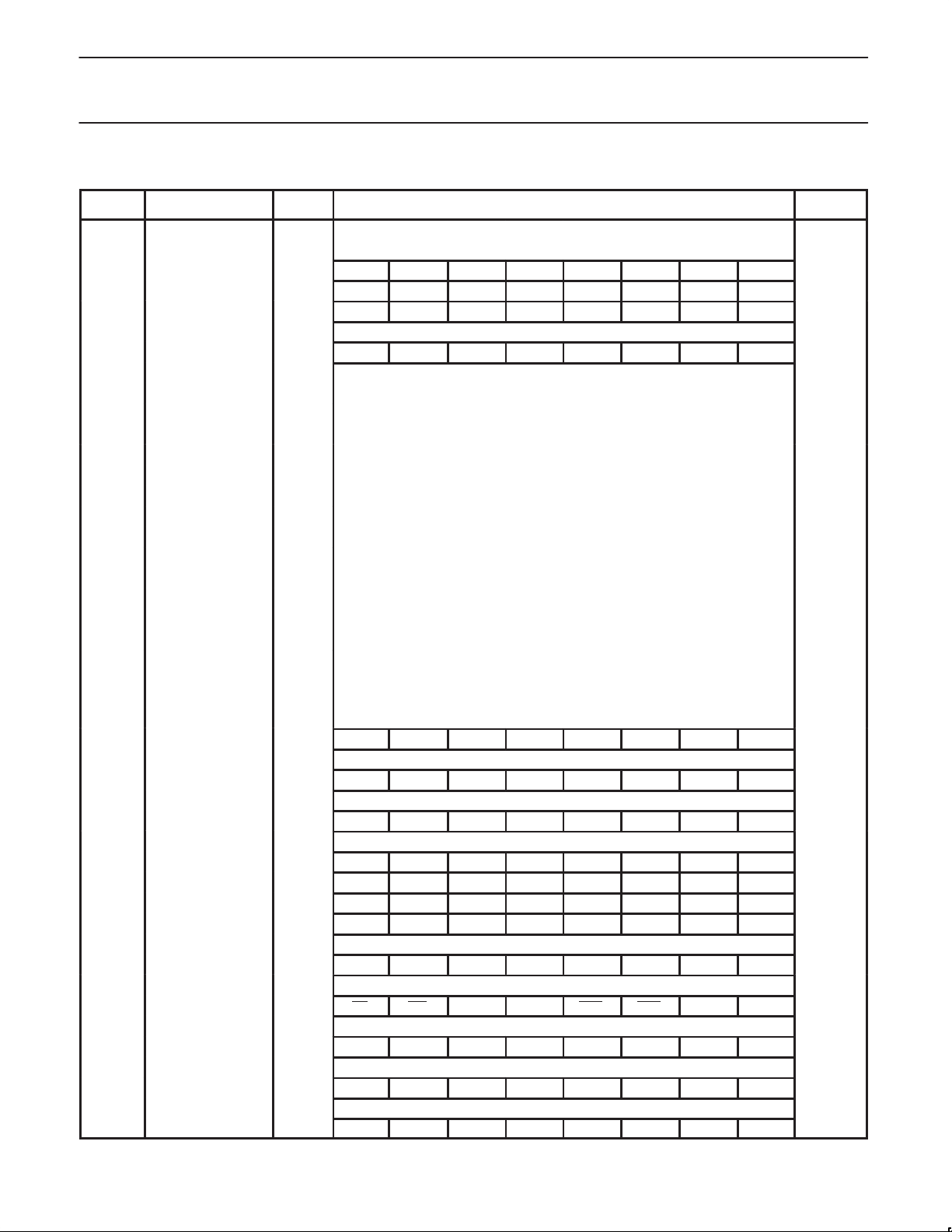
Table 1. 87C554 Special Function Registers
SYMBOL DESCRIPTION
ACC* Accumulator E0H E7 E6 E5 E4 E3 E2 E1 E0 00H
ADCH# A/D converter high C6H xxxxxxxxB
ADCON# A/D control C5H ADC.1 ADC.0 ADEX ADCI ADCS AADR2 AADR1 AADR0 xx000000B
AUXR Auxiliary 8EH – – – – – LVADC EXTRAM A0 xxxxx110B
AUXR1 Auxiliary A2H ADC8 AIDL SRST GF2 WUPD O – DPS 000000x0B
B* B register F0H F7 F6 F5 F4 F3 F2 F1 F0 00H
CTCON# Capture control EBH CTN3 CTP3 CTN2 CTP2 CTN1 CTP1 CTN0 CTP0 00H
CTH3# Capture high 3 CFH xxxxxxxxB
CTH2# Capture high 2 CEH xxxxxxxxB
CTH1# Capture high 1 CDH xxxxxxxxB
CTH0# Capture high 0 CCH xxxxxxxxB
CMH2# Compare high 2 CBH 00H
CMH1# Compare high 1 CAH 00H
CMH0# Compare high 0 C9H 00H
CTL3# Capture low 3 AFH xxxxxxxxB
CTL2# Capture low 2 AEH xxxxxxxxB
CTL1# Capture low 1 ADH xxxxxxxxB
CTL0# Capture low 0 ACH xxxxxxxxB
CML2# Compare low 2 ABH 00H
CML1# Compare low 1 AAH 00H
CML0# Compare low 0 A9H 00H
DPTR:
DPH
DPL
IEN0*# Interrupt enable 0 A8H EA EAD ES1 ES0 ET1 EX1 ET0 EX0 00H
IEN1*# Interrupt enable 1 E8H ET2 ECM2 ECM1 ECM0 ECT3 ECT2 ECT1 ECT0 00H
IP0*# Interrupt priority 0 B8H – PAD PS1 PS0 PT1 PX1 PT0 PX0 x0000000B
IP0H Interrupt priority 0 high B7H – PADH PS1H PS0H PT1H PX1H PT0H PX0H x0000000B
IP1*# Interrupt priority1 F8H PT2 PCM2 PCM1 PCM0 PCT3 PCT2 PCT1 PCT0 00H
IP1H Interrupt priority 1 high F7H PT2H PCM2H PCM1H PCM0H PCT3H PCT2H PCT1H PCT0H 00H
P5# Port 5 C4H ADC7 ADC6 ADC5 ADC4 ADC3 ADC2 ADC1 ADC0 xxxxxxxxB
P4#* Port 4 C0H CMT1 CMT0 CMSR5 CMSR4 CMSR3 CMSR2 CMSR1 CMSR0 FFH
P3* Port 3 B0H RD WR T1 T0 INT1 INT0 TXD RXD FFH
P2* Port 2 A0H A15 A14 A13 A12 A11 A10 A9 A8 FFH
P1* Port 1 90H SDA SCL RT2 T2 CT3I CT2I CT1I CT0I FFH
P0* Port 0 80H AD7 AD6 AD5 AD4 AD3 AD2 AD1 AD0 FFH
Data pointer
(2 bytes):
Data pointer high
Data pointer low
DIRECT
ADDRESS
83H
82H
MSB LSB
AF AE AD AC AB AA A9 A8
EF EE ED EC EB EA E9 E8
BF BE BD BC BB BA B9 B8
FF FE FD FC FB FA F9 F8
C7 C6 C5 C4 C3 C2 C1 C0
B7 B6 B5 B4 B3 B2 B1 B0
A7 A6 A5 A4 A3 A2 A1 A0
97 96 95 94 93 92 91 90
87 86 85 84 83 82 81 80
BIT ADDRESS, SYMBOL, OR ALTERNATIVE PORT FUNCTION
00H
00H
RESET
VALUE
2000 Nov 10
7
Philips Semiconductors Preliminary specification
80C51 8-bit microcontroller – 6 clock operation
16K/512 OTP/ROM/ROMless, 7 channel 10 bit A/D, I2C, PWM,
80C554/83C554/87C554
capture/compare, high I/O, 64L LQFP
00H
00H
00H
00H
00H
00H
RESET
VALUE
SYMBOL
P1M1 Port 1 output mode 1 92H xx000000B
P1M2 Port 1 output mode 2 93H xx000000B
P2M1 Port 2 output mode 1 94H 00H
P2M2 Port 2 output mode 2 95H 00H
P3M1 Port 3 output mode 1 9AH 00H
P3M2 Port 3 output mode 2 9BH 00H
P4M1 Port 4 output mode 1 9CH 00H
P4M2 Port 4 output mode 2 9DH 00H
PCON Power control 87H SMOD1 SMOD0 POF WLE GF1 GFO PD IDL 00x00000B
PSW Program status word D0H CY AC FO RS1 RS0 OV F1 P 00H
PWMP# PWM prescaler FEH 00H
PWM1# PWM register 1 FDH 00H
PWM0# PWM register 0 FCH 00H
RTE# Reset/toggle enable EFH TP47 TP46 RP45 RP44 RP43 RP42 RP41 RP40 00H
S0ADDR Serial 0 slave address F9H 00H
S0ADEN Slave address mask B9H 00H
S0BUF Serial 0 data buffer 99H xxxxxxxxB
S0CON* Serial 0 control 98H SM0/FE SM1 SM2 REN TB8 RB8 TI RI 00H
S1ADR# Serial 1 address DBH SLAVE ADDRESS GC 00H
SIDAT# Serial 1 data DAH 00H
S1STA# Serial 1 status D9H SC4 SC3 SC2 SC1 SC0 0 0 0 F8H
SICON#* Serial 1 control D8H CR2 ENS1 STA ST0 SI AA CR1 CR0 00H
SP Stack pointer 81H 07H
STE# Set enable EEH TG47 TG46 SP45 SP44 SP43 SP42 SP41 SP40 C0H
TH1
TH0
TL1
TL0
TMH2#
TML2#
TMOD Timer mode 89H GA TE C/T M1 M0 GATE C/T M1 M0 00H
TCON* Timer control 88H TF1 TR1 TF0 TR0 IE1 IT1 IE0 IT0 00H
TM2CON# Timer 2 control EAH T2IS1 T2IS0 T2ER T2B0 T2P1 T2P0 T2MS1 T2MS0 00H
TM2IR#* Timer 2 int flag reg C8H T20V CMI2 CMI1 CMI0 CTI3 CTI2 CTI1 CTI0 00H
T3# Timer 3 FFH 00H
DESCRIPTION
Timer high 1
Timer high 0
Timer low 1
Timer low 0
Timer high 2
Timer low 2
DIRECT
ADDRESS
8DH
8CH
8BH
8AH
EDH
ECH
MSB LSB
9F 9E 9D 9C 9B 9A 99 98
DF DE DD DC DB DA D9 D8
8F 8E 8D 8C 8B 8A 89 88
CF CE CD CC CB CA C9 C8
BIT ADDRESS, SYMBOL, OR ALTERNATIVE PORT FUNCTION
* SFRs are bit addressable.
# SFRs are modified from or added to the 80C51 SFRs.
2000 Nov 10
8
Philips Semiconductors Preliminary specification
80C51 8-bit microcontroller – 6 clock operation
16K/512 OTP/ROM/ROMless, 7 channel 10 bit A/D, I2C, PWM,
80C554/83C554/87C554
capture/compare, high I/O, 64L LQFP
OSCILLA T OR CHARACTERISTICS
XTAL1 and XTAL2 are the input and output, respectively , of an
inverting amplifier . The pins can be configured for use as an on-chip
oscillator, as shown in the logic symbol.
To drive the device from an external clock source, XTAL1 should be
driven while XTAL2 is left unconnected. The minimum and maximum
high and low times specified in the data sheet must be observed.
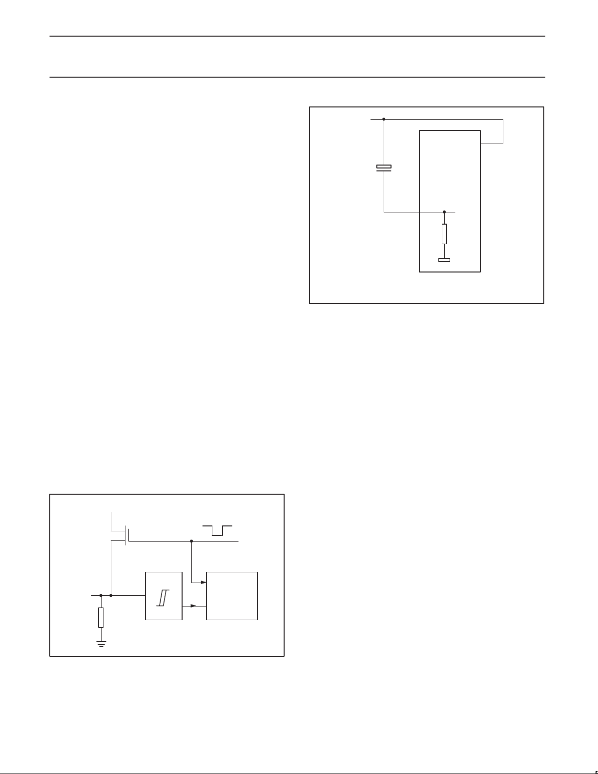
RESET
A reset is accomplished by either (1) externally holding the RST pin
high for at least two machine cycles (12 oscillator periods) or (2)
internally by an on-chip power-on detect (POD) circuit which detects
ramping up from 0 V .
V
CC
To insure a good external power-on reset, the RST pin must be high
long enough for the oscillator to start up (normally a few
milliseconds) plus two machine cycles. The voltage on V
RST pin must come up at the same time for a proper startup.
For a successful internal power-on reset, the V
voltage must
CC
ramp up from 0 V smoothly at a ramp rate greater than 5 V/100 ms.
The RST line can also be pulled HIGH internally by a pull-up
transistor activated by the watchdog timer T3. The length of the
output pulse from T3 is 3 machine cycles. A pulse of such short
duration is necessary in order to recover from a processor or system
fault as fast as possible.
Note that the short reset pulse from Timer T3 cannot discharge the
power-on reset capacitor (see Figure 2). Consequently, when the
watchdog timer is also used to set external devices, this capacitor
arrangement should not be connected to the RST pin, and a
different circuit should be used to perform the power-on reset
operation. A timer T3 overflow, if enabled, will force a reset condition
to the 8xC554 by an internal connection, independent of the level of
the RST pin.
A reset may be performed in software by setting the software reset
bit, SRST (AUXR1.5).
V
DD
SCHMITT
TRIGGER
RST
ON-CHIP
RESISTOR
R
RST
RESET
CIRCUITRY
Figure 1. On-Chip Reset Configuration
and the
DD
OVERFLOW
TIMER T3
SU00952
V
DD
V
DD
2.2 µF
+
8XC554
RST
R
RST
SU00953
Figure 2. Power-On Reset
LOW POWER MODES
Stop Clock Mode
The static design enables the clock speed to be reduced down to
0 MHz (stopped). When the oscillator is stopped, the RAM and
Special Function Registers retain their values. This mode allows
step-by-step utilization and permits reduced system power
consumption by lowering the clock frequency down to any value. For
lowest power consumption the Power Down mode is suggested.
Idle Mode
In the idle mode (see Table 2), the CPU puts itself to sleep while
some of the on-chip peripherals stay active. The instruction to
invoke the idle mode is the last instruction executed in the normal
operating mode before the idle mode is activated. The CPU
contents, the on-chip RAM, and all of the special function registers
remain intact during this mode. The idle mode can be terminated
either by any enabled interrupt (at which time the process is picked
up at the interrupt service routine and continued), or by a hardware
reset which starts the processor in the same manner as a power-on
reset.
Power-Down Mode
To save even more power, a Power Down mode (see Table 2) can
be invoked by software. In this mode, the oscillator is stopped and
the instruction that invoked Power Down is the last instruction
executed. The on-chip RAM and Special Function Registers retain
their values down to 2.0 V and care must be taken to return V
the minimum specified operating voltages before the Power Down
Mode is terminated.
Either a hardware reset or external interrupt can be used to exit from
Power Down. The Wake-up from Power-down bit, WUPD (AUXR1.3)
must be set in order for an external interrupt to cause a wake-up
from power-down. Reset redefines all the SFRs but does not
change the on-chip RAM. An external interrupt allows both the SFRs
and the on-chip RAM to retain their values.
To properly terminate Power Down the reset or external interrupt
should not be executed before V
is restored to its normal
CC
operating level and must be held active long enough for the
oscillator to restart and stabilize (normally less than 10 ms).
CC
to
2000 Nov 10
9

Philips Semiconductors Preliminary specification
80C51 8-bit microcontroller – 6 clock operation
16K/512 OTP/ROM/ROMless, 7 channel 10 bit A/D, I2C, PWM,
80C554/83C554/87C554
capture/compare, high I/O, 64L LQFP
Table 2. External Pin Status During Idle and Power-Down Modes
MODE
Idle Internal 1 1 Data Data Data Data Data High
Idle External 1 1 Float Data Address Data Data High
Power-down Internal 0 0 Data Data Data Data Data High
Power-down External 0 0 Float Data Data Data Data High
PROGRAM
MEMORY
ALE PSEN PORT 0 PORT 1 PORT 2 PORT 3 PORT 4
PWM0/
PWM1
With an external interrupt, INT0 and INT1 must be enabled and
configured as level-sensitive. Holding the pin low restarts the oscillator
but bringing the pin back high completes the exit. Once the interrupt
is serviced, the next instruction to be executed after RETI will be the
one following the instruction that put the device into Power Down.
POWER OFF FLAG
The Power Off Flag (POF) is set by on-chip circuitry when the V
level on the 8xC554 rises from 0 to 5 V. The POF bit can be set or
cleared by software allowing a user to determine if the reset is the
result of a power-on or a warm start after powerdown. The V
must remain above 3 V for the POF to remain unaffected by the V
level.
CC
CC
level
CC
Design Consideration
•When the idle mode is terminated by a hardware reset, the device
normally resumes program execution, from where it left off, up to
two machine cycles before the internal reset algorithm takes
control. On-chip hardware inhibits access to internal RAM in this
event, but access to the port pins is not inhibited. To eliminate
the possibility of an unexpected write when Idle is terminated by
reset, the instruction following the one that invokes Idle should not
be one that writes to a port pin or to external memory.
PCON
(87H)
ONCE Mode
The ONCE (“On-Circuit Emulation”) Mode facilitates testing and
debugging of systems without the device having to be removed from
the circuit. The ONCE Mode is invoked by:
1. Pull ALE low while the device is in reset and PSEN
2. Hold ALE low as RST is deactivated.
While the device is in ONCE Mode, the Port 0 pins go into a float
state, and the other port pins and ALE and PSEN
high. The oscillator circuit remains active. While the device is in this
mode, an emulator or test CPU can be used to drive the circuit.
Normal operation is restored when a normal reset is applied.
is high;
are weakly pulled
Reduced EMI Mode
The ALE-Off bit, AO (AUXR.0) can be set to disable the ALE output.
It will automatically become active when required for external
memory accesses and resume to the OFF state after completing the
external memory access.
01234567
PDGF0GF1WLEPOFSMOD0SMOD1
IDL
(LSB)(MSB)
BIT SYMBOL FUNCTION
PCON.7 SMOD1 Double Baud rate bit. When set to logic 1, the baud rate is doubled when the serial port SIO0 is being
PCON.6 SMOD0 Selects SM0/FE for SCON.7 bit.
PCON.5 POF Power Off Flag
PCON.4 WLE Watchdog Load Enable. This flag must be set by software prior to loading timer T3 (watchdog timer). It is
PCON.3 GF1 General-purpose flag bit.
PCON.2 GF0 General-purpose flag bit.
PCON.1 PD Power-down bit. Setting this bit activates the power-down mode. It can only be set if input EW
PCON.0 IDL Idle mode bit. Setting this bit activates the Idle mode.
If logic 1s are written to PD and IDL at the same time, PD takes precedence. The reset value of PCON is (00X00000).
2000 Nov 10
used in modes 1, 2, or 3.
cleared when timer T3 is loaded.
Figure 3. Power Control Register (PCON)
10
is high.
SU00954

Philips Semiconductors Preliminary specification
80C51 8-bit microcontroller – 6 clock operation
16K/512 OTP/ROM/ROMless, 7 channel 10 bit A/D, I2C, PWM,
80C554/83C554/87C554
capture/compare, high I/O, 64L LQFP
Expanded Data RAM Addressing
The 8xC554 has internal data memory that is mapped into four
separate segments: the lower 128 bytes of RAM, upper 128 bytes of
RAM, 128 byte s S pecial Func tion Regist er (SFR), and 256 bytes
expanded RAM (EXTRAM).
The four segments are:
1. The Lower 128 bytes of RAM (addresses 00H to 7FH) are
directly and indirectly addressable.
2. The Upper 128 bytes of RAM (addresses 80H to FFH) are
indirectly addressable only.
3. The Special Function Registers, SFRs, (addresses 80H to FFH)
are directly addressable only.
4. The 256-bytes expanded RAM (ERAM, 00H – FFH) are indirectly
accessed by move external instruction, MOVX, and with the
EXTRAM bit cleared, see Figure 4.
The Lower 128 bytes can be accessed by either direct or indirect
addressing. The Upper 128 bytes can be accessed by indirect
addressing only . The Upper 128 bytes occupy the same address
space as the SFR. That means they have the same address, but are
physically separate from SFR space.
When an instruction accesses an internal location above address
7FH, the CPU knows whether the access is to the upper 128 bytes
of data RAM or to SFR space by the addressing mode used in the
instruction. Instructions that use direct addressing access SFR
space. For example:
MOV 0A0H,#data
accesses the SFR at location 0A0H (which is P2). Instructions that
use indirect addressing access the Upper 128 bytes of data RAM.
For example:
MOV @R0,#data
where R0 contains 0A0H, accesses the data byte at address 0A0H,
rather than P2 (whose address is 0A0H).
The ERAM can be accessed by indirect addressing, with EXTRAM
bit cleared and MOVX instructions. This part of memory is physically
located on-chip, logically occupies the first 256-bytes of external
data memory.
With EXTRAM = 0, the EXTRAM is indirectly addressed, using the
MOVX instruction in combination with any of the registers R0, R1 of
the selected bank or DPTR. An access to ERAM will not affect ports
P0, P3.6 (WR#) and P3.7 (RD#). P2 SFR is output during expanded
RAM addressing. For example, with EXTRAM = 0,
MOVX @R0,#data
where R0 contains 0A0H, accesses the ERAM at address 0A0H
rather than external memory. An access to external data memory
locations higher than FFH (i.e., 0100H to FFFFH) will be performed
with the MOVX DPTR instructions in the same way as in the
standard 80C51, so with P0 and P2 as data/address bus, and P3.6
and P3.7 as write and read timing signals. Refer to Figure 5.
With EXTRAM = 1, MOVX @Ri and MOVX @DPTR will be similar
to the standard 80C51. MOVX @ Ri will provide an 8-bit address
multiplexed with data on Port 0 and any output port pins can be
used to output higher order address bits. This is to provide the
external paging capability. MOVX @DPTR will generate a 16-bit
address. Port 2 outputs the high-order eight address bits (the
contents of DPH) while Port 0 multiplexes the low-order eight
address bits (DPL) with data. MOVX @Ri and MOVX @DPTR will
generate either read or write signals on P3.6 (#WR) and P3.7 (#RD).
The stack pointer (SP) may be located anywhere in the 256 bytes
RAM (lower and upper RAM) internal data memory. The stack may
not be located in the ERAM address space.
AUXR
Symbol Function
AO Disable/Enable ALE
EXTRAM Internal/External RAM (00H – FFH) access using MOVX @Ri/@DPTR
LVADC Enable A/D low voltage operation
— Not implemented, reserved for future use*.
NOTE:
*User software should not write 1s to reserved bits. These bits may be used in future 8051 family products to invoke new features. In that
case, the reset or inactive value of the new bit will be 0, and its active value will be 1. The value read from a reserved bit is indeterminate.
Address = 8EH
Not Bit Addressable
— ————LVADC EXTRAM AO
Bit:
AO Operating Mode
0 ALE is emitted at a constant rate of 1/6 the oscillator frequency.
1 ALE is active only during a MOVX or MOVC instruction.
EXTRAM Operating Mode
0 Internal ERAM (00H–FFH) access using MOVX @Ri/@DPTR
1 External data memory access.
LVADC Operating Mode
0 Turns off A/D charge pump.
1 Turns on A/D charge pump. Required for operation below 4V.
76543210
Figure 4. AUXR: Auxiliary Register
Reset Value = xxxx x110B
SU00979A
2000 Nov 10
11
Philips Semiconductors Preliminary specification
80C51 8-bit microcontroller – 6 clock operation
16K/512 OTP/ROM/ROMless, 7 channel 10 bit A/D, I2C, PWM,
80C554/83C554/87C554
capture/compare, high I/O, 64L LQFP
FF
ERAM
256 BYTES
00
FF
UPPER
128 BYTES
INTERNAL RAM
80 80
LOWER
128 BYTES
INTERNAL RAM
00
Figure 5. Internal and External Data Memory Address Space with EXTRAM = 0
Dual DPTR
The dual DPTR structure (see Figure 6) is a way by which the chip
will specify the address of an external data memory location. There
are two 16-bit DPTR registers that address the external memory,
and a single bit called DPS = AUXR1/bit0 that allows the program
code to switch between them.
The DPS bit status should be saved by software when switching
between DPTR0 and DPTR1.
DPS
BIT0
AUXR1
DPH
(83H)
DPL
(82H)
Figure 6.
DPTR1
DPTR0
EXTERNAL
DATA
MEMORY
SU00745A
FF
SPECIAL
FUNCTION
REGISTER
00
FFFF
0100
0000
EXTERNAL
DATA
MEMORY
SU00980
Note that bit 2 is not writable and is always read as a zero. This
allows the DPS bit to be quickly toggled simply by executing an
INC AUXR1 instruction without affecting the other bits.
DPTR Instructions
The instructions that refer to DPTR refer to the data pointer that is
currently selected using the AUXR1/bit 0 register. The six
instructions that use the DPTR are as follows:
INC DPTR Increments the data pointer by 1
MOV DPTR, #data16 Loads the DPTR with a 16-bit constant
MOV A, @ A+DPTR Move code byte relative to DPTR to ACC
MOVX A, @ DPTR Move external RAM (16-bit address) to
ACC
MOVX @ DPTR , A Move ACC to external RAM (16-bit
address)
JMP @ A + DPTR Jump indirect relative to DPTR
The data pointer can be accessed on a byte-by-byte basis by
specifying the low or high byte in an instruction which accesses the
SFRs. See application note AN458 for more details.
2000 Nov 10
12

Philips Semiconductors Preliminary specification
80C51 8-bit microcontroller – 6 clock operation
16K/512 OTP/ROM/ROMless, 7 channel 10 bit A/D, I2C, PWM,
80C554/83C554/87C554
capture/compare, high I/O, 64L LQFP
AUXR1
Symbol Function
DPS Data Pointer Switch—switches between DPRT0 and DPTR1.
WUPD Enable wakeup from powerdown.
GF2 General Purpose Flag—set and cleared by the user .
SRST Software Reset
AIDL Enables the ADC during idle mode.
ADC8 ADC Mode Switch—switches between 10-bit conversion and 8-bit conversion.
NOTE:
*User software should not write 1s to reserved bits. These bits may be used in future 8051 family products to invoke new features. In that
case, the reset or inactive value of the new bit will be 0, and its active value will be 1. The value read from a reserved bit is indeterminate.
Address = A2H
Not Bit Addressable
ADC8 AIDL SRST GF2 WUPD 0 — DSP
Bit:
DPS Operating Mode
0 DPTR0
1 DPTR1
ADC8 Operating Mode
0 10-bit conversion (50 machine cycles)
1 8-bit conversion (24 machine cycles)
76543210
Figure 7. AUXR1: DPTR Control Register
Reset Value = 0000 00x0B
SU01081
2000 Nov 10
13

Philips Semiconductors Preliminary specification
80C51 8-bit microcontroller – 6 clock operation
16K/512 OTP/ROM/ROMless, 7 channel 10 bit A/D, I2C, PWM,
80C554/83C554/87C554
capture/compare, high I/O, 64L LQFP
Enhanced UART
The UART operates in all of the usual modes that are described in
the first section of
Microcontrollers
detect by looking for missing stop bits, and automatic address
recognition. The UART also fully supports multiprocessor
communication as does the standard 80C51 UART.
When used for framing error detect the UART looks for missing stop
bits in the communication. A missing bit will set the FE bit in the
S0CON register. The FE bit shares the S0CON.7 bit with SM0 and
the function of S0CON.7 is determined by PCON.6 (SMOD0) (see
Figure 8). If SMOD0 is set then S0CON.7 functions as FE.
S0CON.7 functions as SM0 when SMOD0 is cleared. When used as
FE S0CON.7 can only be cleared by software. Refer to Figure 9.
Automatic Address Recognition
Automatic Address Recognition is a feature which allows the UART
to recognize certain addresses in the serial bit stream by using
Symbol Function
Data Handbook IC20, 80C51-Based 8-Bit
. In addition the UART can perform framing error
S0CON Address = 98H
Bit Addressable
SM0/FE SM1 SM2 REN TB8 RB8 Tl Rl
Bit: 76543210
(SMOD0 = 0/1)*
hardware to make the comparisons. This feature saves a great deal
of software overhead by eliminating the need for the software to
examine every serial address which passes by the serial port. This
feature is enabled by setting the SM2 bit in S0CON. In the 9 bit
UART modes, mode 2 and mode 3, the Receive Interrupt flag (RI)
will be automatically set when the received byte contains either the
“Given” address or the “Broadcast” address. The 9 bit mode
requires that the 9th information bit is a 1 to indicate that the
received information is an address and not data. Automatic address
recognition is shown in Figure 10.
The 8 bit mode is called Mode 1. In this mode the RI flag will be set
if SM2 is enabled and the information received has a valid stop bit
following the 8 address bits and the information is either a Given or
Broadcast address.
Reset Value = 0000 0000B
FE Framing Error bit. This bit is set by the receiver when an invalid stop bit is detected. The FE bit is not cleared by valid
frames but should be cleared by software. The SMOD0 bit must be set to enable access to the FE bit.
SM0 Serial Port Mode Bit 0, (SMOD0 must = 0 to access bit SM0)
SM1 Serial Port Mode Bit 1
SM0 SM1 Mode Description Baud Rate**
0 0 0 shift register f
OSC
/6
0 1 1 8-bit UART variable
1 0 2 9-bit UART f
OSC
/32 or f
OSC
/16
1 1 3 9-bit UART variable
SM2 Enables the Automatic Address Recognition feature in Modes 2 or 3. If SM2 = 1 then Rl will not be set unless the
received 9th data bit (RB8) is 1, indicating an address, and the received byte is a Given or Broadcast Address.
In Mode 1, if SM2 = 1 then Rl will not be activated unless a valid stop bit was received, and the received byte is a
Given or Broadcast Address. In Mode 0, SM2 should be 0.
REN Enables serial reception. Set by software to enable reception. Clear by software to disable reception.
TB8 The 9th data bit that will be transmitted in Modes 2 and 3. Set or clear by software as desired.
RB8 In modes 2 and 3, the 9th data bit that was received. In Mode 1, if SM2 = 0, RB8 is the stop bit that was received.
In Mode 0, RB8 is not used.
Tl Transmit interrupt flag. Set by hardware at the end of the 8th bit time in Mode 0, or at the beginning of the stop bit in the
other modes, in any serial transmission. Must be cleared by software.
Rl Receive interrupt flag. Set by hardware at the end of the 8th bit time in Mode 0, or halfway through the stop bit time in
the other modes, in any serial reception (except see SM2). Must be cleared by software.
NOTE:
*SMOD0 is located at PCON6.
= oscillator frequency
**f
OSC
Figure 8. S0CON: Serial Port Control Register
SU01445
2000 Nov 10
14
Philips Semiconductors Preliminary specification
80C51 8-bit microcontroller – 6 clock operation
16K/512 OTP/ROM/ROMless, 7 channel 10 bit A/D, I2C, PWM,
80C554/83C554/87C554
capture/compare, high I/O, 64L LQFP
D0 D1 D2 D3 D4 D5 D6 D7 D8
START
BIT
SM0 / FE SM1 SM2 REN TB8 RB8 TI RI
SMOD1 SMOD0 POF WLE GF1 GF0 PD IDL
0 : S0CON.7 = SM0
1 : S0CON.7 = FE
DATA BYTE
SET FE BIT IF STOP BIT IS 0 (FRAMING ERROR)
SM0 TO UART MODE CONTROL
Figure 9. UART Framing Error Detection
D0 D1 D2 D3 D4 D5 D6 D7 D8
SM0 SM1 SM2 REN TB8 RB8 TI RI
1
1
1
0
11 X
ONLY IN
MODE 2, 3
SCON
(98H)
PCON
(87H)
STOP
BIT
SU00982
SCON
(98H)
RECEIVED ADDRESS D0 TO D7
PROGRAMMED ADDRESS
IN UART MODE 2 OR MODE 3 AND SM2 = 1:
INTERRUPT IF REN=1, RB8=1 AND “RECEIVED ADDRESS” = “PROGRAMMED ADDRESS”
– WHEN OWN ADDRESS RECEIVED, CLEAR SM2 TO RECEIVE DATA BYTES
– WHEN ALL DATA BYTES HAVE BEEN RECEIVED: SET SM2 TO WAIT FOR NEXT ADDRESS.
Figure 10. UART Multiprocessor Communication, Automatic Address Recognition
Mode 0 is the Shift Register mode and SM2 is ignored.
Using the Automatic Address Recognition feature allows a master to
selectively communicate with one or more slaves by invoking the
Given slave address or addresses. All of the slaves may be
contacted by using the Broadcast address. Two special Function
Registers are used to define the slave’s address, SADDR, and the
address mask, SADEN. SADEN is used to define which bits in the
SADDR are to b used and which bits are “don’t care”. The SADEN
mask can be logically ANDed with the SADDR to create the “Given”
address which the master will use for addressing each of the slaves.
Use of the Given address allows multiple slaves to be recognized
while excluding others. The following examples will help to show the
versatility of this scheme:
Slave 0 SADDR = 1100 0000
SADEN = 1111 1101
Given = 1100 00X0
COMPARATOR
SU00045
Slave 1 SADDR = 1100 0000
SADEN = 1111 1110
Given = 1100 000X
In the above example SADDR is the same and the SADEN data is
used to differentiate between the two slaves. Slave 0 requires a 0 in
bit 0 and it ignores bit 1. Slave 1 requires a 0 in bit 1 and bit 0 is
ignored. A unique address for Slave 0 would be 1100 0010 since
slave 1 requires a 0 in bit 1. A unique address for slave 1 would be
1100 0001 since a 1 in bit 0 will exclude slave 0. Both slaves can be
selected at the same time by an address which has bit 0 = 0 (for
slave 0) and bit 1 = 0 (for slave 1). Thus, both could be addressed
with 1100 0000.
2000 Nov 10
15

Philips Semiconductors Preliminary specification
80C51 8-bit microcontroller – 6 clock operation
16K/512 OTP/ROM/ROMless, 7 channel 10 bit A/D, I2C, PWM,
80C554/83C554/87C554
capture/compare, high I/O, 64L LQFP
In a more complex system the following could be used to select
slaves 1 and 2 while excluding slave 0:
Slave 0 SADDR = 1100 0000
SADEN = 1111 1001
Given = 1100 0XX0
Slave 1 SADDR = 1110 0000
Slave 2 SADDR = 1110 0000
In the above example the differentiation among the 3 slaves is in the
lower 3 address bits. Slave 0 requires that bit 0 = 0 and it can be
uniquely addressed by 1110 01 10. Slave 1 requires that bit 1 = 0 and
it can be uniquely addressed by 1110 and 0101. Slave 2 requires
that bit 2 = 0 and its unique address is 1110 0011. To select Slaves 0
and 1 and exclude Slave 2 use address 1110 0100, since it is
necessary to make bit 2 = 1 to exclude slave 2.
The Broadcast Address for each slave is created by taking the
logical OR of SADDR and SADEN. Zeros in this result are trended
as don’t-cares. In most cases, interpreting the don’t-cares as ones,
the broadcast address will be FF hexadecimal.
Upon reset SADDR (SFR address 0A9H) and SADEN (SFR
address 0B9H) are leaded with 0s. This produces a given address
of all “don’t cares” as well as a Broadcast address of all “don’t
cares”. This effectively disables the Automatic Addressing mode and
allows the microcontroller to use standard 80C51 type UART drivers
which do not make use of this feature.
Timer T2
Timer T2 is a 16-bit timer consisting of two registers TMH2 (HIGH
byte) and TML2 (LOW byte). The 16-bit timer/counter can be
switched off or clocked via a prescaler from one of two sources:
f
/6 or an external signal. When Timer T2 is configured as a
OSC
counter, the prescaler is clocked by an external signal on T2 (P1.4).
A rising edge on T2 increments the prescaler, and the maximum
repetition rate is one count per machine cycle (0.5 MHz with a
12 MHz oscillator).
The maximum repetition rate for Timer T2 is twice the maximum
repetition rate for Timer 0 and Timer 1. T2 (P1.4) is sampled at
S2P1 and again at S5P1 (i.e., twice per machine cycle). A rising
edge is detected when T2 is LOW during one sample and HIGH
during the next sample. To ensure that a rising edge is detected, the
input signal must be LOW for at least 1/2 cycle and then HIGH for at
least 1/2 cycle. If a rising edge is detected before the end of S2P1,
the timer will be incremented during the following cycle; otherwise it
will be incremented one cycle later. The prescaler has a
programmable division factor of 1, 2, 4, or 8 and is cleared if its
division factor or input source is changed, or if the timer/counter is
reset.
Timer T2 may be read “on the fly” but possesses no extra read
latches, and software precautions may have to be taken to avoid
misinterpretation in the event of an overflow from least to most
significant byte while Timer T2 is being read. Timer T2 is not
loadable and is reset by the RST signal or by a rising edge on the
input signal RT2, if enabled. RT2 is enabled by setting bit T2ER
(TM2CON.5).
When the least significant byte of the timer overflows or when a
16-bit overflow occurs, an interrupt request may be generated.
SADEN = 1111 1010
Given = 11 10 0X0X
SADEN = 1111 1100
Given = 1110 00XX
Either or both of these overflows can be programmed to request an
interrupt. In both cases, the interrupt vector will be the same. When
the lower byte (TML2) overflows, flag T2B0 (TM2CON) is set and
flag T20V (TM2IR) is set when TMH2 overflows. These flags are set
one cycle after an overflow occurs. Note that when T20V is set,
T2B0 will also be set. To enable the byte overflow interrupt, bits ET2
(IEN1.7, enable overflow interrupt, see Figure 11) and T2IS0
(TM2CON.6, byte overflow interrupt select) must be set. Bit TWB0
(TM2CON.4) is the Timer T2 byte overflow flag.
To enable the 16-bit overflow interrupt, bits ET2 (IE1.7, enable
overflow interrupt) and T2IS1 (TM2CON.7, 16-bit overflow interrupt
select) must be set. Bit T2OV (TM2IR.7) is the Timer T2 16-bit
overflow flag. All interrupt flags must be reset by software. To enable
both byte and 16-bit overflow, T2IS0 and T2IS1 must be set and two
interrupt service routines are required. A test on the overflow flags
indicates which routine must be executed. For each routine, only the
corresponding overflow flag must be cleared.
Timer T2 may be reset by a rising edge on RT2 (P1.5) if the Timer
T2 external reset enable bit (T2ER) in T2CON is set. This reset also
clears the prescaler. In the idle mode, the timer/counter and
prescaler are reset and halted. Timer T2 is controlled by the
TM2CON special function register (see Figure 12).
Timer T2 Extension: When a 6 MHz oscillator is used, a 16-bit
overflow on Timer T2 occurs every 65.5, 131, 262, or 524 ms,
depending on the prescaler division ratio; i.e., the maximum cycle
time is approximately 0.5 seconds. In applications where cycle times
are greater than 0.5 seconds, it is necessary to extend Timer T2.
This is achieved by selecting fosc/12 as the clock source (set
T2MS0, reset T2MS1), setting the prescaler division ration to 1/8
(set T2P0, set T2P1), disabling the byte overflow interrupt (reset
T2IS0) and enabling the 16-bit overflow interrupt (set T2IS1). The
following software routine is written for a three-byte extension which
gives a maximum cycle time of approximately 2400 hours.
OVINT: PUSH ACC ;save accumulator
PUSH PSW ;save status
INC TIMEX1 ;increment first byte (low order)
;of extended timer
MOV A,TIMEX1
JNZ INTEX ;jump to INTEX if ;there is no overflow
INC TIMEX2 ;increment second byte
MOV A,TIMEX2
JNZ INTEX ;jump to INTEX if there is no overflow
INC TIMEX3 ;increment third byte (high order)
INTEX: CLR T2OV ;reset interrupt flag
POP PSW ;restore status
POP ACC ;restore accumulator
RETI ;return from interrupt
Timer T2, Capture and Compare Logic: Timer T2 is connected to
four 16-bit capture registers and three 16-bit compare registers. A
capture register may be used to capture the contents of Timer T2
when a transition occurs on its corresponding input pin. A compare
register may be used to set, reset, or toggle port 4 output pins at
certain pre-programmable time intervals.
The combination of Timer T2 and the capture and compare logic is
very powerful in applications involving rotating machinery,
automotive injection systems, etc. Timer T2 and the capture and
compare logic are shown in Figure 13.
2000 Nov 10
16

Philips Semiconductors Preliminary specification
80C51 8-bit microcontroller – 6 clock operation
16K/512 OTP/ROM/ROMless, 7 channel 10 bit A/D, I2C, PWM,
80C554/83C554/87C554
capture/compare, high I/O, 64L LQFP
IEN1 (E8H)
TM2CON (EAH)
01234567
ECT1ECT2ECT3ECM0ECM1ECM2ET2
BIT SYMBOL FUNCTION
IEN1.7 ET2 Enable Timer T2 overflow interrupt(s)
IEN1.6 ECM2 Enable T2 Comparator 2 interrupt
IEN1.5 ECM1 Enable T2 Comparator 1 interrupt
IEN1.4 ECM0 Enable T2 Comparator 0 interrupt
IEN1.3 ECT3 Enable T2 Capture register 3 interrupt
IEN1.2 ECT2 Enable T2 Capture register 2 interrupt
IEN1.1 ECT1 Enable T2 Capture register 1 interrupt
IEN1.0 ECT0 Enable T2 Capture register 0 interrupt
Figure 11. Timer T2 Interrupt Enable Register (IEN1)
T2MS1T2P0T2P1T2BOT2ERT2IS0T2IS1
BIT SYMBOL FUNCTION
TM2CON.7 TSIS1 Timer T2 16-bit overflow interrupt select
TM2CON.6 T2IS0 Timer T2 byte overflow interrupt select
TM2CON.5 T2ER Timer T2 external reset enable. When this bit is set,
TM2CON.4 T2BO Timer T2 byte overflow interrupt flag
TM2CON.3 T2P1
TM2CON.2 T2P0
Timer T2 may be reset by a rising edge on RT2 (P1.5).
Timer T2 prescaler select
ECT0
(LSB)(MSB)
01234567
T2MS0
(LSB)(MSB)
Reset Value = 00H
SU01083
Reset Value = 00H
T2P1 T2P0 Timer T2 Clock
0 0 Clock source
0 1 Clock source/2
1 0 Clock source/4
1 1 Clock source/8
TM2CON.1 T2MS1
TM2CON.0 T2MS0
T2MS1 T2MS0 Mode Selected
0 0 Timer T2 halted (off)
0 1 T2 clock source = f
1 0 Test mode; do not use
1 1 T2 clock source = pin T2
Figure 12. T2 Control Register (TM2CON)
Timer T2 mode select
OSC
/6
SU01446
2000 Nov 10
17

Philips Semiconductors Preliminary specification
80C51 8-bit microcontroller – 6 clock operation
16K/512 OTP/ROM/ROMless, 7 channel 10 bit A/D, I2C, PWM,
80C554/83C554/87C554
capture/compare, high I/O, 64L LQFP
off
f
osc
T2
RT2
T2ER
External reset
S
S
S
S
S
S
TG
TG
STE RTE
1/6
enable
INTCT0I
CTI0
CT0 CT1 CT2 CT3
Prescaler T2 Counter
R
R
R
R
R
R
T
T
P4.0
P4.1
P4.2
P4.3
P4.4
P4.5
P4.6
P4.7
I/O port 4
CT1I
CT2I
CTI1
COMP
CMO (S)
S = set
R = reset
T = toggle
TG = toggle status
INTINT
CTI2
8-bit overflow interrupt
16-bit overflow interrupt
INT
T2 SFR address:
COMP
CM1 (R)
TML2 = lower 8 bits
TMH2 = higher 8 bits
Figure 13. Block Diagram of Timer 2
INT
CT3I
COMP
CM2 (T)
INT
CTI3
INT
SU01447
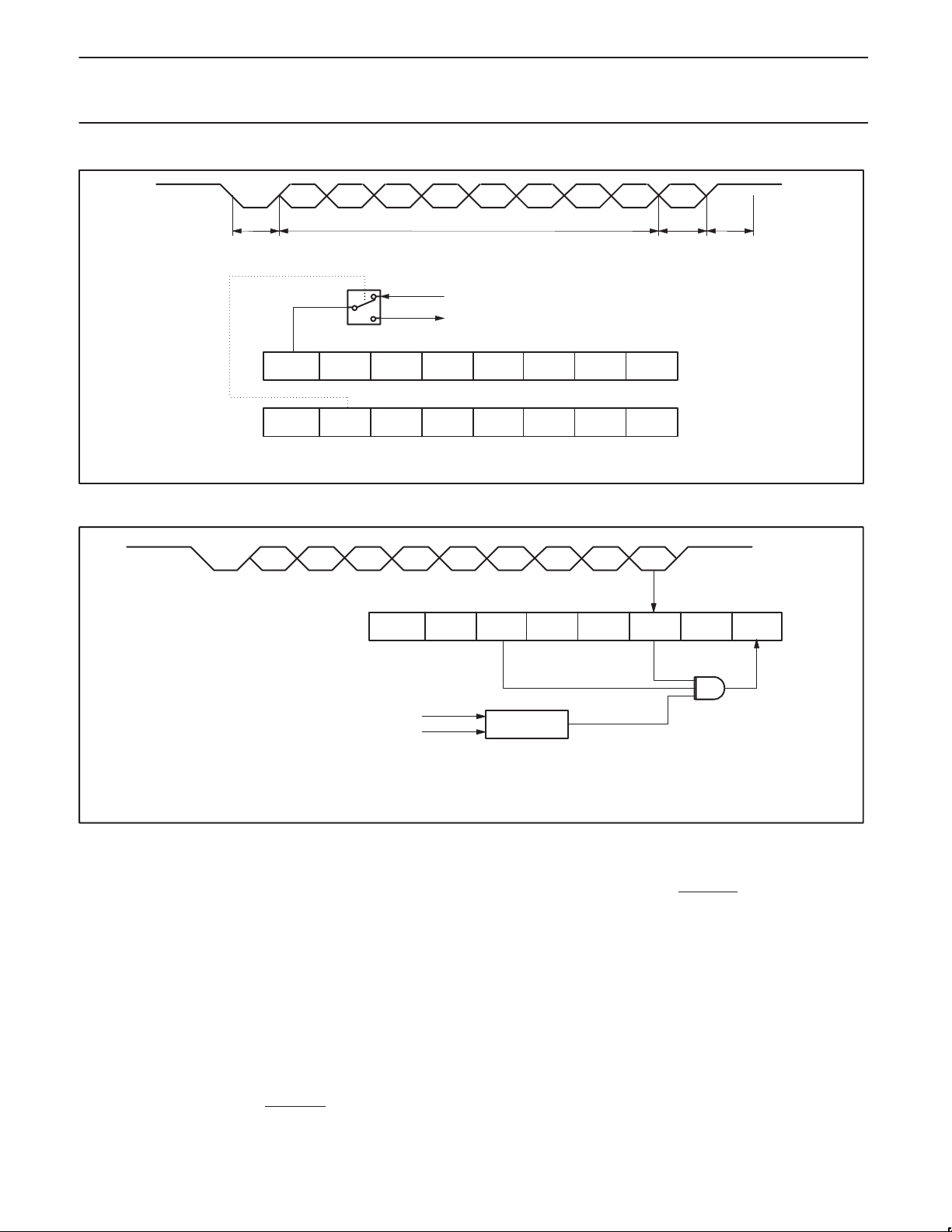
Capture Logic: The four 16-bit capture registers that Timer T2 is
connected to are: CT0, CT1, CT2, and CT3. These registers are
loaded with the contents of Timer T2, and an interrupt is requested
upon receipt of the input signals CT0I, CT1I, CT2I, or CT3I. These
input signals are shared with port 1. The four interrupt flags are in
the Timer T2 interrupt register (TM2IR special function register). If
the capture facility is not required, these inputs can be regarded as
additional external interrupt inputs.
Using the capture control register CTCON (see Figure 14), these
inputs may capture on a rising edge, a falling edge, or on either a
rising or falling edge. The inputs are sampled during S1P1 of each
cycle. When a selected edge is detected, the contents of Timer T2
are captured at the end of the cycle.
Measuring Time Intervals Using Capture Registers: When a
recurring external event is represented in the form of rising or falling
edges on one of the four capture pins, the time between two events
can be measured using Timer T2 and a capture register . When an
event occurs, the contents of Timer T2 are copied into the relevant
capture register and an interrupt request is generated. The interrupt
service routine may then compute the interval time if it knows the
previous contents of Timer T2 when the last event occurred. With a
12 MHz oscillator, T imer T2 can be programmed to overflow every
524 ms. When event interval times are shorter than this, computing
the interval time is simple, and the interrupt service routine is short.
For longer interval times, the Timer T2 extension routine may be
used.
Compare Logic: Each time Timer T2 is incremented, the contents
of the three 16-bit compare registers CM0, CM1, and CM2 are
compared with the new counter value of Timer T2. When a match is
found, the corresponding interrupt flag in TM2IR is set at the end of
the following cycle. When a match with CM0 occurs, the controller
sets bits 0-5 of port 4 if the corresponding bits of the set enable
register STE are at logic 1.
2000 Nov 10
18

Philips Semiconductors Preliminary specification
80C51 8-bit microcontroller – 6 clock operation
16K/512 OTP/ROM/ROMless, 7 channel 10 bit A/D, I2C, PWM,
80C554/83C554/87C554
capture/compare, high I/O, 64L LQFP
CTCON (EBH)
BIT SYMBOL CAPTURE/INTERRUPT ON:
CTCON.7 CTN3 Capture Register 3 triggered by a falling edge on CT3I
CTCON.6 CTP3 Capture Register 3 triggered by a rising edge on CT3I
CTCON.5 CTN2 Capture Register 2 triggered by a falling edge on CT2I
CTCON.4 CTP2 Capture Register 2 triggered by a rising edge on CT2I
CTCON.3 CTN1 Capture Register 1 triggered by a falling edge on CT1I
CTCON.2 CTP1 Capture Register 1 triggered by a rising edge on CT1I
CTCON.1 CTN0 Capture Register 0 triggered by a falling edge on CT0I
CTCON.0 CTP0 Capture Register 0 triggered by a rising edge on CT0I
Figure 14. Capture Control Register (CTCON)
When a match with CM1 occurs, the controller resets bits 0-5 of port
4 if the corresponding bits of the reset/toggle enable register RTE
are at logic 1 (see Figure 15 for RTE register function). If RTE is “0”,
then P4.n is not affected by a match between CM1 or CM2 and
Timer 2. When a match with CM2 occurs, the controller “toggles”
bits 6 and 7 of port 4 if the corresponding bits of the RTE are at
logic 1. The port latches of bits 6 and 7 are not toggled.
Two additional flip-flops store the last operation, and it is these
flip-flops that are toggled.
Thus, if the current operation is “set,” the next operation will be
“reset” even if the port latch is reset by software before the “reset”
operation occurs. The first “toggle” after a chip RESET will set the
port latch. The contents of these two flip-flops can be read at STE.6
and STE.7 (corresponding to P4.6 and P4.7, respectively). Bits
STE.6 and STE.7 are read only (see Figure 16 for STE register
function). A logic 1 indicates that the next toggle will set the port
latch; a logic 0 indicates that the next toggle will reset the port latch.
CM0, CM1, and CM2 are reset by the RST signal.
The modified port latch information appears at the port pin during
S5P1 of the cycle following the cycle in which a match occurred. If
the port is modified by software, the outputs change during S1P1 of
the following cycle. Each port 4 bit can be set or reset by software at
any time. A hardware modification resulting from a comparator
match takes precedence over a software modification in the same
cycle. When the comparator results require a “set” and a “reset” at
the same time, the port latch will be reset.
01234567
CTN1CTP1CTN1CTP2CTN2CTP3CTN3
Timer T2 Interrupt Flag Register TM2IR: Eight of the nine Timer
T2 interrupt flags are located in special function register TM2IR (see
Figure 17). The ninth flag is TM2CON.4.
The CT0I and CT1I flags are set during S4 of the cycle in which the
contents of Timer T2 are captured. CT0I is scanned by the interrupt
logic during S2, and CT1I is scanned during S3. CT2I and CT3I are
set during S6 and are scanned during S4 and S5. The associated
interrupt requests are recognized during the following cycle. If these
flags are polled, a transition at CT0I or CT1I will be recognized one
cycle before a transition on CT2I or CT3I since registers are read
during S5. The CMI0, CMI1, and CMI2 flags are set during S6 of the
cycle following a match. CMI0 is scanned by the interrupt logic
during S2; CMI1 and CMI2 are scanned during S3 and S4. A match
will be recognized by the interrupt logic (or by polling the flags) two
cycles after the match takes place.
The 16-bit overflow flag (T2OV) and the byte overflow flag (T2BO)
are set during S6 of the cycle in which the overflow occurs. These
flags are recognized by the interrupt logic during the next cycle.
Special function register IP1 (Figure 17) is used to determine the
Timer T2 interrupt priority. Setting a bit high gives that function a
high priority , and setting a bit low gives the function a low priority.
The functions controlled by the various bits of the IP1 register are
shown in Figure 17.
CTP0
(LSB)(MSB)
Reset Value = 00H
SU01085
2000 Nov 10
RTE (EFH)
01234567
RO41RP42RP43RP44RP45TP46TP47
BIT SYMBOL FUNCTION
RTE.7 TP47 If “1” then P4.7 toggles on a match between CM1 and Timer T2
RTE.6 TP46 If “1” then P4.6 toggles on a match between CM1 and Timer T2
RTE.5 RP45 If “1” then P4.5 is reset on a match between CM1 and Timer T2
RTE.4 RP44 If “1” then P4.4 is reset on a match between CM1 and Timer T2
RTE.3 RP43 If “1” then P4.3 is reset on a match between CM1 and Timer T2
RTE.2 RP42 If “1” then P4.2 is reset on a match between CM1 and Timer T2
RTE.1 RP41 If “1” then P4.1 is reset on a match between CM1 and Timer T2
RTE.0 RP40 If “1” then P4.0 is reset on a match between CM1 and Timer T2
Figure 15. Reset/Toggle Enable Register (RTE)
19
RP40
(LSB)(MSB)
Reset Value = 00H
SU01086

Philips Semiconductors Preliminary specification
80C51 8-bit microcontroller – 6 clock operation
16K/512 OTP/ROM/ROMless, 7 channel 10 bit A/D, I2C, PWM,
80C554/83C554/87C554
capture/compare, high I/O, 64L LQFP
STE (EEH)
TM2IR (C8H)
01234567
SP41SP42SP43SP44SP45TG46TG47
BIT SYMBOL FUNCTION
STE.7 TG47 Toggle flip-flops
STE.6 TG46 Toggle flip-flops
STE.5 SP45 If “1” then P4.5 is set on a match between CM0 and Timer T2
STE.4 SP44 If “1” then P4.4 is set on a match between CM0 and Timer T2
STE.3 SP43 If “1” then P4.3 is set on a match between CM0 and Timer T2
STE.2 SP42 If “1” then P4.2 is set on a match between CM0 and Timer T2
STE.1 SP41 If “1” then P4.1 is set on a match between CM0 and Timer T2
STE.0 SP40 If “1” then P4.0 is set on a match between CM0 and Timer T2
Figure 16. Set Enable Register (STE)
CTI1CTI2CTI3CMI0CMI1CMI2T2OV
BIT SYMBOL FUNCTION
TM2IR.7 T2OV Timer T2 16-bit overflow interrupt flag
TM2IR.6 CMI2 CM2 interrupt flag
TM2IR.5 CMI1 CM1 interrupt flag
TM2IR.4 CMI0 CM0 interrupt flag
TM2IR.3 CTI3 CT3 interrupt flag
TM2IR.2 CTI2 CT2 interrupt flag
TM2IR.1 CTI1 CT1 interrupt flag
TM2IR.0 CTI0 CT0 interrupt flag
SP40
(LSB)(MSB)
01234567
CTI0
(LSB)(MSB)
Reset Value = C0H
SU01087
Reset Value = 00H
Interrupt Flag Register (TM2IR)
01234567
IP1 (F8H)
BIT SYMBOL FUNCTION
IP1.7 PT2 Timer T2 overflow interrupt(s) priority level
IP1.6 PCM2 Timer T2 comparator 2 interrupt priority level
IP1.5 PCM1 Timer T2 comparator 1 interrupt priority level
IP1.4 PCM0 Timer T2 comparator 0 interrupt priority level
IP1.3 PCT3 Timer T2 capture register 3 interrupt priority level
IP1.2 PCT2 Timer T2 capture register 2 interrupt priority level
IP1.1 PCT1 Timer T2 capture register 1 interrupt priority level
IP1.0 PCT0 Timer T2 capture register 0 interrupt priority level
Timer 2 Interrupt Priority Register (IP1)
Figure 17. Interrupt Flag Register (TM2IR) and Timer T2 Interrupt Priority Register (IP1)
PCT1PCT2PCT3PCM0PCM1PCM2PT2
PCT0
(LSB)(MSB)
Reset Value = 00H
SU01088
2000 Nov 10
20
Philips Semiconductors Preliminary specification
80C51 8-bit microcontroller – 6 clock operation
16K/512 OTP/ROM/ROMless, 7 channel 10 bit A/D, I2C, PWM,
80C554/83C554/87C554
capture/compare, high I/O, 64L LQFP
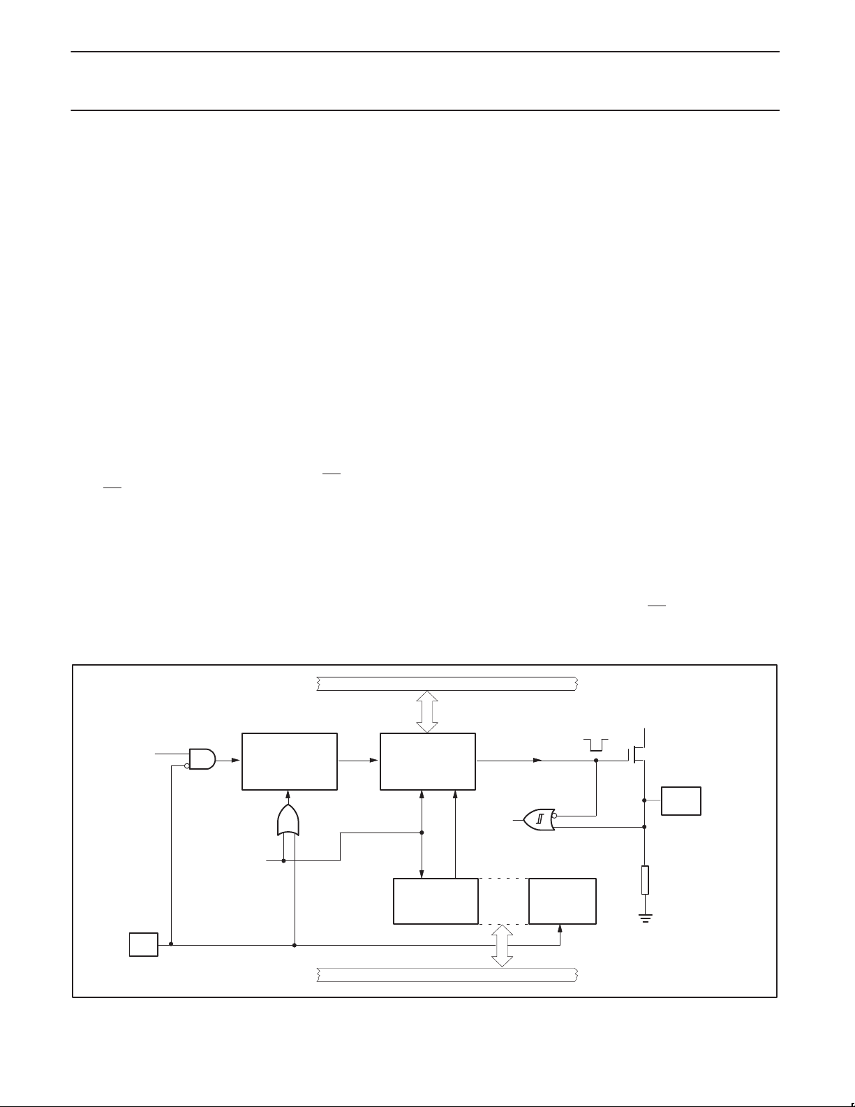
Timer T3, The Watchdog T imer
In addition to Timer T2 and the standard timers, a watchdog timer is
also incorporated on the 8xC554. The purpose of a watchdog timer
is to reset the microcontroller if it enters erroneous processor states
(possibly caused by electrical noise or RFI) within a reasonable
period of time. An analogy is the “dead man’s handle” in railway
locomotives. When enabled, the watchdog circuitry will generate a
system reset if the user program fails to reload the watchdog timer
within a specified length of time known as the “watchdog interval.”
Watchdog Circuit Description: The watchdog timer (Timer T3)
consists of an 8-bit timer with an 11-bit prescaler as shown in
Figure 18. The prescaler is fed with a signal whose frequency is 1/6
the oscillator frequency (0.5 MHz with a 12 MHz oscillator). The 8-bit
timer is incremented every “t” seconds, where:
t = 6 × 2048 × 1/f
(= 0.75 ms at f
OSC
= 16 MHz; = 0.5 ms at f
OSC
= 24 MHz)
OSC
If the 8-bit timer overflows, a short internal reset pulse is generated
which will reset the 8xC554. A short output reset pulse is also
generated at the RST pin. This short output pulse (3 machine
cycles) may be destroyed if the RST pin is connected to a capacitor.
This would not, however, affect the internal reset operation.
Watchdog operation is activated when external pin EW
When EW
is tied low, it is impossible to disable the watchdog
is tied low.
operation by software.
How to Operate the Watchdog Timer: The watchdog timer has to
be reloaded within periods that are shorter than the programmed
watchdog interval; otherwise the watchdog timer will overflow and a
system reset will be generated. The user program must therefore
continually execute sections of code which reload the watchdog
timer. The period of time elapsed between execution of these
sections of code must never exceed the watchdog interval. When
using a 16 MHz oscillator, the watchdog interval is programmable
between 0.75 ms and 196 ms. When using a 24 MHz oscillator, the
watchdog interval is programmable between 0.5 ms and 127.5 ms.
In order to prepare software for watchdog operation, a programmer
should first determine how long his system can sustain an
erroneous processor state. The result will be the maximum
watchdog interval. As the maximum watchdog interval becomes
shorter, it becomes more dif ficult for the programmer to ensure that
the user program always reloads the watchdog timer within the
watchdog interval, and thus it becomes more difficult to implement
watchdog operation.
The programmer must now partition the software in such a way that
reloading of the watchdog is carried out in accordance with the above
requirements. The programmer must determine the execution times
of all software modules. The effect of possible conditional branches,
subroutines, external and internal interrupts must all be taken into
account. Since it may be very difficult to evaluate the execution
times of some sections of code, the programmer should use worst
case estimations. In any event, the programmer must make sure
that the watchdog is not activated during normal operation.
The watchdog timer is reloaded in two stages in order to prevent
erroneous software from reloading the watchdog. First PCON.4
(WLE) must be set. The T3 may be loaded. When T3 is loaded,
PCON.4 (WLE) is automatically reset. T3 cannot be loaded if
PCON.4 (WLE) is reset. Reload code may be put in a subroutine as
it is called frequently. Since Timer T3 is an up-counter, a reload
value of 00H gives the maximum watchdog interval (255 ms with a
12 MHz oscillator), and a reload value of 0FFH gives the minimum
watchdog interval (1 ms with a 12 MHz oscillator).
In the idle mode, the watchdog circuitry remains active. When
watchdog operation is implemented, the power-down mode cannot
be used since both states are contradictory. Thus, when watchdog
operation is enabled by tying external pin EW
low, it is impossible to
enter the power-down mode, and an attempt to set the power-down
bit (PCON.1) will have no effect. PCON.1 will remain at logic 0.
f
2000 Nov 10
OSC
/6
EW
PRESCALER (11-BIT)
WRITE T3
CLEAR
INTERNAL BUS
TIMER T3 (8-BIT)
LOAD LOADEN
INTERNAL
RESET
CLEAR
WLE
PCON.4 PCON.1
INTERNAL BUS
Figure 18. Watchdog Timer
21
OVERFLOW
LOADEN
PD
V
DD
P
RST
R
RST
SU00955

Philips Semiconductors Preliminary specification
80C51 8-bit microcontroller – 6 clock operation
16K/512 OTP/ROM/ROMless, 7 channel 10 bit A/D, I2C, PWM,
80C554/83C554/87C554
capture/compare, high I/O, 64L LQFP
During the early stages of software development/debugging, the
watchdog may be disabled by tying the EW
stage, EW
may be tied low to complete the debugging process.
pin high. At a later
Watchdog Software Example: The following example shows how
watchdog operation might be handled in a user program.
;at the program start:
T3 EQU 0FFH ;address of watchdog timer T3
PCON EQU 087H ;address of PCON SFR
WATCH-INTV EQU 156 ;watchdog interval (e.g., 100 ms)
;to be inserted at each watchdog reload location within
;the user program:
LCALL WATCHDOG
;watchdog service routine:
WATCHDOG: ORL PCON,#10H ;set condition flag (PCON.4)
MOV T3,WATCH-INV ;load T3 with watchdog interval
RET
If it is possible for this subroutine to be called in an erroneous state,
then the condition flag WLE should be set at different parts of the
main program.
Serial I/O
The 8xC554 is equipped with two independent serial ports: SIO0
and SIO1. SIO0 is a full duplex UART port and is similar to the
Enhanced UART serial port. SIO1 accommodates the I
2
C bus.
SIO0: SIO0 is a full duplex serial I/O port identical to that of the
Enhanced UART except Time 2 cannot be used as a baud rate
generator. Its operation is the same, including the use of timer 1 as a
baud rate generator.
Port 5 Operation
Port 5 may be used to input up to 8 analog signals to the ADC.
Unused ADC inputs may be used to input digital inputs. These
inputs have an inherent hysteresis to prevent the input logic from
drawing excessive current from the power lines when driven by
analog signals. Channel to channel crosstalk (Ct) should be taken
into consideration when both analog and digital signals are
simultaneously input to Port 5 (see, D.C. characteristics in data
sheet).
Port 5 is not bidirectional and may not be configured as an output
port. All six ports are multifunctional, and their alternate functions
are listed in the Pin Descriptions section of this datasheet.
Pulse Width Modulated Outputs
The 8xC554 contains two pulse width modulated output channels
(see Figure 19). These channels generate pulses of programmable
length and interval. The repetition frequency is defined by an 8-bit
prescaler PWMP, which supplies the clock for the counter. The
prescaler and counter are common to both PWM channels. The 8-bit
counter counts modulo 255, i.e., from 0 to 254 inclusive. The value
of the 8-bit counter is compared to the contents of two registers:
PWM0 and PWM1. Provided the contents of either of these registers
is greater than the counter value, the corresponding PWM0
PWM1
output is set LOW. If the contents of these registers are
or
equal to, or less than the counter value, the output will be HIGH. The
pulse-width-ratio is therefore defined by the contents of the registers
PWM0 and PWM1. The pulse-width-ratio is in the range of 0 to 1
and may be programmed in increments of 1/255.
Buffered PWM outputs may be used to drive DC motors. The
rotation speed of the motor would be proportional to the contents of
PWMn. The PWM outputs may also be configured as a dual DAC. In
this application, the PWM outputs must be integrated using
conventional operational amplifier circuitry. If the resulting output
voltages have to be accurate, external buffers with their own analog
supply should be used to buffer the PWM outputs before they are
integrated. The repetition frequency f
, at the PWMn outputs is
PWM
give by:
f
f
PWM
+
OSC
(1 ) PWMP) 255
This gives a repetition frequency range of 246 Hz to 62.8 kHz
(f
= 16 MHz). At f
OSC
= 24 MHz, the frequency range is 368 Hz
OSC
to 83.4 Hz. By loading the PWM registers with either 00H or FFH,
the PWM channels will output a constant HIGH or LOW level,
respectively. Since the 8-bit counter counts modulo 255, it can never
actually reach the value of the PWM registers when they are loaded
with FFH.
When a compare register (PWM0 or PWM1) is loaded with a new
value, the associated output is updated immediately. It does not
have to wait until the end of the current counter period. Both PWMn
output pins are driven by push-pull drivers. These pins are not used
for any other purpose.
Prescaler frequency control register PWMP Reset Value = 00H
PWMP (FEH) 765 43210
MSB LSB
PWMP.0-7 Prescaler division factor = PWMP + 1.
Reading PWMP gives the current reload value. The actual count of
the prescaler cannot be read.
Reset Value = 00H
WM0 (FCH)
PWM1 (FDH)
PWM0/1.0-7} Low/high ratio of PWMn +
765 43 2 10
MSB LSB
(PWMn)
255 * (PWMn)
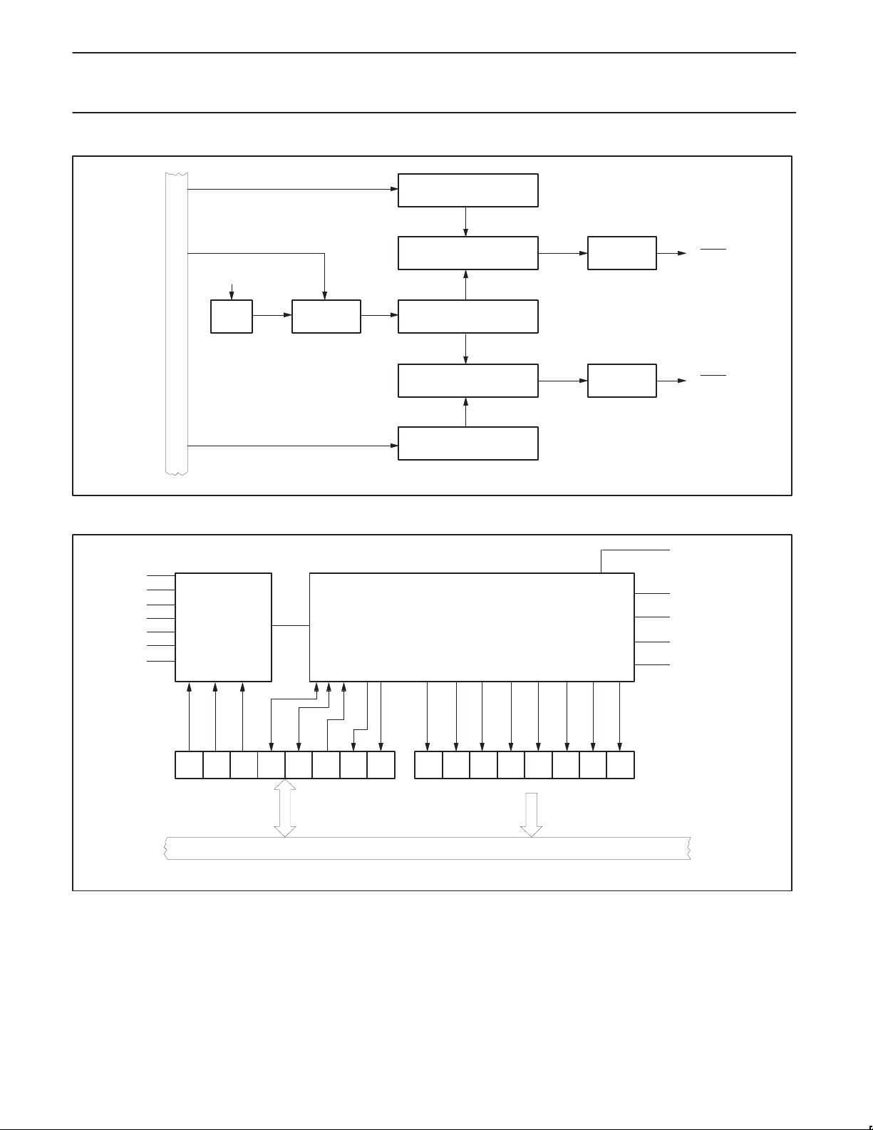
Analog-to-Digital Converter
The analog input circuitry consists of an 8-input analog multiplexer
and a 10-bit, straight binary, successive approximation ADC. The
A/D can also be operated in 8-bit mode with faster conversion times
by setting bit ADC8 (AUXR1.7). The 8-bit results will be contained in
the ADCH register. The analog reference voltage and analog power
supplies are connected via separate input pins. For 10-bit accuracy,
the conversion takes 50 machine cycles, i.e., 18.75 µs at an
oscillator frequency of 16 MHz, 12.5 µs at an oscillator frequency of
24 MHz. For the 8-bit mode, the conversion takes 24 machine
cycles. Input voltage swing is from 0 V to +5 V. Because the internal
DAC employs a ratiometric potentiometer, there are no
discontinuities in the converter characteristic. Figure 20 shows a
functional diagram of the analog input circuitry.
The ADC has the option of either being powered off in idle mode for
reduced power consumption or being active in idle mode for
reducing internal noise during the conversion. This option is selected
by the AIDL bit of AUXR1 register (AUXR1.6). With the AIDL bit set,
the ADC is active in the idle mode, and with the AIDL bit cleared, the
ADC is powered off in idle mode.
2000 Nov 10
22
Philips Semiconductors Preliminary specification
80C51 8-bit microcontroller – 6 clock operation
16K/512 OTP/ROM/ROMless, 7 channel 10 bit A/D, I2C, PWM,
80C554/83C554/87C554
capture/compare, high I/O, 64L LQFP
PWM0
ADC0
ADC1
ADC2
ADC3
ADC4
ADC5
ADC6
INTERNAL BUS
MULTIPLEXER
8-BIT COMPARATOR
f
OSC
PRESCALER
PWMP
8-BIT COUNTER
8-BIT COMPARATOR
PWM1
Figure 19. Functional Diagram of Pulse Width Modulated Outputs
10-BIT A/D CONVERTERANALOG INPUT
OUTPUT
BUFFER
OUTPUT
BUFFER
PWM0
PWM1
SU01448
STADC
+
ANALOG REF.
–
ANALOG SUPPLY
ANALOG GROUND
ADCON ADCH
01234567 01234567
INTERNAL BUS
Figure 20. Functional Diagram of Analog Input Circuitry
10-Bit Analog-to-Digital Conversion: Figure 21 shows the
elements of a successive approximation (SA) ADC. The ADC
contains a DAC which converts the contents of a successive
approximation register to a voltage (VDAC) which is compared to
the analog input voltage (Vin). The output of the comparator is fed to
the successive approximation control logic which controls the
successive approximation register. A conversion is initiated by
setting ADCS in the ADCON register. ADCS can be set by software
only or by either hardware or software.
2000 Nov 10
SU01467
The software only start mode is selected when control bit ADCON.5
(ADEX) = 0. A conversion is then started by setting control bit
ADCON.3 (ADCS). The hardware or software start mode is selected
when ADCON.5 = 1, and a conversion may be started by setting
ADCON.3 as above or by applying a rising edge to external pin
STADC. When a conversion is started by applying a rising edge, a
low level must be applied to STADC for at least one machine cycle
followed by a high level for at least one machine cycle.
23
 Loading...