

Philips P80C528FFA, P80C528FFAA, P80C528FFB, P80C528FFBB, P80C528FFP Datasheet
...
80C528/83C528
CMOS single-chip 8-bit microcontroller
Product specification 1995 Feb 02
INTEGRATED CIRCUITS
IC20 Data Handbook

Philips Semiconductors Product specification
80C528/83C528CMOS single-chip 8-bit microcontrollers
2
1995 Feb 02
DESCRIPTION
The 8XC528 single-chip 8-bit microcontroller
is manufactured in an advanced CMOS
process and is a derivative of the 80C51
microcontroller family. The 8XC528 has the
same instruction set as the 80C51. Three
versions of the derivative exist:
•83C528 — 32k bytes mask programmable
ROM
•80C528 — ROMless version of the
83C528
•87C528 — 32k bytes EPROM (described
in a separate data sheet)
This device provides architectural
enhancements that make it applicable in a
variety of applications in consumer, telecom
and general control systems, especially in
those systems which need large ROM and
RAM capacity on-chip.
The 8XC528 contains a 32k × 8 ROM
(83C528), a 512 × 8 RAM, four 8-bit I/O
ports, two 16-bit timer/event counters
(identical to the timers of the 80C51), a 16-bit
timer (identical to the timer 2 of the 80C52), a
watchdog timer with a separate oscillator, a
multi-source, two-priority-level, nested
interrupt structure, two serial interfaces
(UART and I
2
C-bus), and on-chip oscillator
and timing circuits.
In addition, the 8XC528 has two software
selectable modes of power reduction — idle
mode and power-down mode. The idle mode
freezes the CPU while allowing the RAM,
timers, serial port, and interrupt system to
continue functioning. The power-down mode
saves the RAM contents but freezes the
oscillator, causing all other chip functions to
be inoperative.
FEATURES
•80C51 instruction set
– 32k × 8 ROM (83C528)
– ROMless (80C528)
– 512 × 8 RAM
– Memory addressing capability
64k ROM and 64k RAM
– Three 16-bit counter/timers
– On-chip watchdog timer with oscillator
– Full duplex UART
– I
2
C serial interface
– Four 8-bit I/O ports
•Power control modes:
– Idle mode
– Power-down mode
– Warm start from power-down
•CMOS and TTL compatible
•Extended temperature ranges
•ROM code protection
•7-source and 7-vector interrupt structure
with 2 priority levels
•Up to 3 external interrupt request inputs
•Two programmable power reduction modes
(Idle and Power-down)
•Termination of Idle mode by any interrupt,
external or WDT (watchdog) reset
•XTAL frequency range: 1.2 MHz to 16 MHz
PIN CONFIGURATIONS
1
2
3
4
5
6
7
8
9
10
11
12
13
14
15
16
17
18
19
20
21
22
23
24
25
26
27
28
29
30
31
32
33
34
35
36
37
38
39
40
T2/P1.0
T2EX/P1.1
P1.2
P1.3
P1.4
P1.5
SCL/P1.6
RST
RxD/P3.0
TxD/P3.1
INT0/P3.2
INT1
/P3.3
T0/P3.4
T1/P3.5
SDA/P1.7
WR
/P3.6
RD/P3.7
XTAL2
XTAL1
V
SS
P2.0/A8
P2.1/A9
P2.2/A10
P2.3/A11
P2.4/A12
P2.5/A13
P2.6/A14
P2.7/A15
PSEN
ALE
EA
P0.7/AD7
P0.6/AD6
P0.5/AD5
P0.4/AD4
P0.3/AD3
P0.2/AD2
P0.1/AD1
P0.0/AD0
V
DD
DUAL
IN-LINE
PACKAGE
QUAD
FLAT
PACK
44
34
1
11
33
23
12 22
LEADED
CHIP
CARRIER
6 1 40
7
17
39
29
18 28
1
2
3
4
5
6
7
8
9
10
11
12
13
14
15
16
17
18
19
20
23
24
25
26
27
28
29
30
31
32
33
34
35
36
37
38
39
40
41
42
T2/P1.0
T2EX/P1.1
P1.2
P1.3
P1.4
P1.5
SCL/P1.6
RST
RxD/P3.0
TxD/P3.1
INT0
/P3.2
INT1
/P3.3
T0/P3.4
T1/P3.5
SDA/P1.7
WR
/P3.6
RD
/P3.7
XTAL2
XTAL1
P2.1/A9
P2.2/A10
P2.3/A11
P2.4/A12
P2.5/A13
P2.6/A14
P2.7/A15
PSEN
ALE
EA
P0.7/AD7
P0.6/AD6
P0.5/AD5
P0.4/AD4
P0.3/AD3
P0.2/AD2
P0.1/AD1
P0.0/AD0
V
DD
SHRINK
DUAL
IN-LINE
PACKAGE
21
22
V
SS
P2.0/A8
NC*
NC*
* DO NOT CONNECT

Philips Semiconductors Product specification
80C528/83C528CMOS single-chip 8-bit microcontrollers
1995 Feb 02
3
CERAMIC AND PLASTIC LEADED
CHIP CARRIER PIN FUNCTIONS
6 1 40
7
17
39
29
18 28
PLCC
Pin Function Pin Function
1 NC* 23 NC*
2 P1.0/T2 24 P2.0/A8
3 P1.1/T2EX 25 P2.1/A9
4 P1.2 26 P2.2/A10
5 P1.3 27 P2.3/A11
6 P1.4 28 P2.4/A12
7 P1.5 29 P2.5/A13
8 P1.6/SCL 30 P2.6/A14
9 P1.7/SDA 31 P2.7/A15
10 RST 32 PSEN
11 P3.0/RxD 33 ALE
12 NC* 34 NC*
13 P3.1/TxD 35 EA
14 P3.2/INT0 36 P0.7/AD7
15 P3.3/INT1 37 P0.6/AD6
16 P3.4/T0 38 P0.5/AD5
17 P3.5/T1 39 P0.4/AD4
18 P3.6/WR 40 P0.3/AD3
19 P3.7/RD 41 P0.2/AD2
20 XTAL2 42 P0.1/AD1
21 XTAL1 43 P0.0/AD0
22 V
SS
44 V
DD
* DO NOT CONNECT
PLASTIC QUAD FLAT PACK
PIN FUNCTIONS
44 34
1
11
33
23
12 22
PQFP
Pin Function Pin Function
1 P1.5 23 P2.5/A13
2 P1.6/SCL 24 P2.6/A14
3 P1.7/SDA 25 P2.7/A15
4 RST 26 PSEN
5 P3.0/RxD 27 ALE
6 NC* 28 NC*
7 P3.1/TxD 29 EA
8 P3.2/INT0 30 P0.7/AD7
9 P3.3/INT1 31 P0.6/AD6
10 P3.4/T0 32 P0.5/AD5
11 P3.5/T1 33 P0.4/AD4
12 P3.6/WR 34 P0.3/AD3
13 P3.7RD 35 P0.2/AD2
14 XTAL2 36 P0.1/AD1
15 XTAL1 37 P0.0/AD0
16 V
SS
38 V
DD
17 NC* 39 NC*
18 P2.0/A8 40 P1.0/T2
19 P2.1/A9 41 P1.1/T2EX
20 P2.2/A10 42 P1.2
21 P2.3/A11 43 P1.3
22 P2.4/A12 44 P1.4
* DO NOT CONNECT
LOGIC SYMBOL
PORT 0
PORT 1PORT 2
PORT 3
ADDRESS AND
DATA BUS
ADDRESS BUS
T2
T2EX
RxD
TxD
INT0
INT1
T0
T1
WR
RD
SECONDARY FUNCTIONS
RST
EA
PSEN
ALE
V
SS
V
DD
XTAL1
XTAL2
SCL
SDA

Philips Semiconductors Product specification
80C528/83C528CMOS single-chip 8-bit microcontrollers
1995 Feb 02
4
ORDERING INFORMATION
PHILIPS
PART ORDER NUMBER
PART MARKING
PHILIPS NORTH AMERICA
PART ORDER
NUMBER
ROMless ROM ROMless ROM
Drawing
Number
TEMPERATURE oC RANGE
AND PACKAGE
FREQ
MHz
P80C528FBP P83C528FBP/xxx P80C528FBP N P83C528FBP N SOT129-1 0 to +70, Plastic Dual In-line Package 16
P80C528FBA P83C528FBA/xxx P80C528FBA A P83C528FBA A SOT187-2 0 to +70, Plastic Leaded Chip Carrier 16
P80C528FBB P83C528FBB/xxx P80C528FBB B P83C528FBB B SOT307-2 0 to +70, Plastic Quad Flat Pack 16
P80C528FFP P83C528FFP/xxx P80C528FFP N P83C528FFP N SOT129-1 –40 to +85, Plastic Dual In-line Package 16
P80C528FFA P83C528FFA/xxx P80C528FFA A P83C528FFA A SOT187-2 –40 to +85, Plastic Leaded Chip Carrier 16
P80C528FFB P83C528FFB/xxx P80C528FFB B P83C528FFB B SOT307-2 –40 to +85, Plastic Quad Flat Pack 16
P80C528FHP P83C528FHP/xxx P80C528FHP N P83C528FHP N SOT129-1 –40 to +125, Plastic Dual In-line Package 16
P80C528FHA P83C528FHA/xxx P80C528FHA A P83C528FHA A SOT187-2 –40 to +125, Plastic Leaded Chip Carrier 16
P80C528FHB P83C528FHB/xxx P80C528FHB B P83C528FHB B SOT307-2 –40 to +125, Plastic Quad Flat Pack 16
P83C528FBR/xxx SOT270-1 0 to +70, Plastic Shrink Dual In-Linr Package 16
NOTE:
1. xxx denotes the ROM code number.

Philips Semiconductors Product specification
80C528/83C528CMOS single-chip 8-bit microcontrollers
1995 Feb 02
5
EPROM
Drawing
Number
TEMPERATURE oC RANGE
AND PACKAGE
FREQ
MHz
P87C528EBP N SOT129-1 0 to +70, Plastic Dual In-line Package 16
P87C528EBF FA 0590B
0 to +70, Ceramic Dual In-line Package
w/Window
16
P87C528EBA AA SOT187-2 0 to +70, Plastic Leaded Chip Carrier 16
P87C528EBL KA 1472A
0 to +70, Ceramic Leaded Chip Carrier
w/Window
16
P87C528EBB B SOT307-2 0 to +70, Plastic Quad Flat Pack 16
P87C528EFP N SOT129-1 –40 to +85, Plastic Dual In-line Package 16
P87C528EFF FA 0590B
–40 to +85, Ceramic Dual In-line Package
w/Window
16
P87C528EFF FA SOT187-2 –40 to +85, Plastic Leaded Chip Carrier 16
P87C528EFL KA 1472A
–40 to +85, Ceramic Leaded Chip Carrier
w/Window
16
P87C528EFB B SOT307-2 –40 to +85, Plastic Quad Flat Pack 16
P87C528GBP N SOT129-1 0 to +70, Plastic Dual In-line Package 20
P87C528GBF FA 0590B
0 to +70, Ceramic Dual In-line Package
w/Window
20
P87C528GBA A SOT187-2 0 to +70, Plastic Leaded Chip Carrier 20
P87C528GBL KA 1472A
0 to +70, Ceramic Leaded Chip Carrier
w/Window
20
P87C528GFP N SOT129-1 –40 to +85, Plastic Dual In-line Package 20
P87C528GFF FA 0590B
–40 to +85, Ceramic Dual In-line Package
w/Window
20
P87C528GFA A SOT187-2 –40 to +85, Plastic Leaded Chip Carrier 20
P87C528GFL KA 1472A
–40 to +85, Ceramic Leaded Chip Carrier
w/Window
20

Philips Semiconductors Product specification
80C528/83C528CMOS single-chip 8-bit microcontrollers
1995 Feb 02
6
BLOCK DIAGRAM
PROGRAMMABLE I/O
CPU
T0 T1
COUNTERS
XTAL2 XTAL1
INT0
INT1
CONTROL
SERIAL IN SERIAL OUT
OSCILLATOR
AND
TIMING
PROGRAM
MEMORY
(32K x 8 ROM)
RAM AUX–RAM
DATA
MEMORY
(256 x 8)
TWO 16-BIT
TIMER/EVENT
COUNTERS
DATA
MEMORY
(256 x 8)
16-BIT TIMER /
EVENT COUNTER
WATCHDOG
TIMER
64K-BYTE BUS
EXPANSION
CONTROL
PROGRAMMABLE
SERIAL PORT
FULL DUPLEX UART
SYNCHRONOUS SHIFT
BIT-LEVEL
I
2
C
INTERFACE
FREQUENCY
REFERENCE
T2 T2EX
RST
EXTERNAL
INTERRUPTS
PARALLEL PORTS,
ADDRESS/DATA BUS
AND I/O PINS
SHARED WITH
PORT 3
INTERNAL
INTERRUPTS
SDA SCL

Philips Semiconductors Product specification
80C528/83C528CMOS single-chip 8-bit microcontrollers
1995 Feb 02
7
PIN DESCRIPTION
PIN NO.
MNEMONIC DIP SDIL LCC QFP TYPE NAME AND FUNCTION
V
SS
20 21 22 16 I Ground: circuit ground potential.
V
DD
40 42 44 38 I Power Supply: +5V power supply pin during normal operation, Idle mode and
Power-down mode.
P0.0–0.7 39–32 41–34 43–36 37–30 I/O Port 0: Port 0 is an open-drain, bidirectional I/O port. Port 0 pins that have 1s
written to them float and can be used as high-impedance inputs. Port 0 is also the
multiplexed low-order address and data bus during accesses to external program
and data memory. In this application, it uses strong internal pull-ups when emitting
1s.
P1.0–P1.7 1–8 1–8 2–9 40–44
1–3
I/O Port 1: Port 1 is an 8-bit bidirectional I/O port with internal pull-ups, except P1.6 and
P1.7 which have open drain. Port 1 pins that have 1s written to them are pulled high
by the internal pull-ups and can be used as inputs. As inputs, port 1 pins that are
externally pulled low will source current because of the internal pull-ups. (See DC
Electrical Characteristics: I
IL
). Port 1 can sink/source one TTL (4 LSTTL) inputs.
1 1 2 40 I T2 (P1.0): Timer/counter 2 external count input (following edge triggered).
2 2 3 41 I T2EX (P1.1): Timer/counter 2 trigger input.
7 7 8 2 I/O SCL (P1.6): I2C serial port clock line.
8 8 9 3 I/O SDA (P1.7): I2C serial port data line.
P2.0–P2.7 21–28 22–29 24–31 18–25 I/O Port 2: Port 2 is an 8-bit bidirectional I/O port with internal pull-ups. Port 2 pins that
have 1s written to them are pulled high by the internal pull-ups and can be used as
inputs. As inputs, port 2 pins that are externally being pulled low will source current
because of the internal pull-ups. (See DC Electrical Characteristics: I
IL
). Port 2
emits the high-order address byte during fetches from external program memory
and during accesses to external data memory that use 16-bit addresses (MOVX
@DPTR). In this application, it uses strong internal pull-ups when emitting 1s.
During accesses to external data memory that use 8-bit addresses (MOV @Ri), port
2 emits the contents of the P2 special function register.
P3.0–P3.7 10–17 10–18
(11=NC)
11,
13–19
5,
7–13
I/O Port 3: Port 3 is an 8-bit bidirectional I/O port with internal pull-ups. Port 3 pins that
have 1s written to them are pulled high by the internal pull-ups and can be used as
inputs. As inputs, port 3 pins that are externally being pulled low will source current
because of the pull-ups. (See DC Electrical Characteristics: I
IL
). Port 3 also serves
the special features of the SC80C51 family, as listed below:
10 10 11 5 I RxD (P3.0): Serial input port
11 12 13 7 O TxD (P3.1): Serial output port
12 13 14 8 I INT0 (P3.2): External interrupt
13 14 15 9 I INT1 (P3.3): External interrupt
14 15 16 10 I T0 (P3.4): Timer 0 external input
15 16 17 11 I T1 (P3.5): Timer 1 external input
16 17 18 12 O WR (P3.6): External data memory write strobe
17 18 19 13 O RD (P3.7): External data memory read strobe
RST 9 9 10 4 I/O Reset: A high on this pin for two machine cycles while the oscillator is running,
resets the device. An internal diffused resistor to V
SS
permits a power-on reset
using only an external capacitor to V
DD
. After a watchdog timer overflow, this pin is
pulled high while the internal reset signal is active.
ALE 30 31 33 27 I/O Address Latch Enable: Output pulse for latching the low byte of the address
during an access to external memory. In normal operation, ALE is emitted at a
constant rate of 1/6 the oscillator frequency, and can be used for external timing or
clocking. Note that one ALE pulse is skipped during each access to external data
memory.
PSEN 29 30 32 26 O Program Store Enable: The read strobe to external program memory. When the
device is executing code from the external program memory, PSEN
is activated
twice each machine cycle, except that two PSEN
activations are skipped during
each access to external data memory. PSEN
is not activated during fetches from
internal program memory.
EA 31 33 35 29 I External Access Enable: EA must be externally held low during RESET to enable
the device to fetch code from external program memory locations 0000H to 7FFFH.
If EA
is held high during RESET, the device executes from internal program memory
unless the program counter contains an address greater than 7FFFH. EA
is don’t
care after RESET.
XTAL1 19 20 21 15 I Crystal 1: Input to the inverting oscillator amplifier and input to the internal clock
generator circuits.
XTAL2 18 19 20 14 O Crystal 2: Output from the inverting oscillator amplifier.
Philips Semiconductors Product specification
80C528/83C528CMOS single-chip 8-bit microcontrollers
1995 Feb 02
8
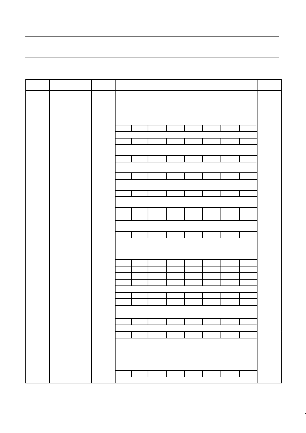
Table 1. 8XC524/8XC528 Special Function Registers
SYMBOL DESCRIPTION
DIRECT
ADDRESS
BIT ADDRESS, SYMBOL, OR ALTERNATIVE PORT FUNCTION
MSB LSB
RESET
VALUE
ACC* Accumulator E0H E7 E6 E5 E4 E3 E2 E1 E0 00H
B* B register F0H F7 F6 F5 F4 F3 F2 F1 F0 00H
DPTR:
DPH
DPL
Data pointer (2 bytes):
Data pointer high
Data pointer low
83H
82H
00H
00H
AF AE AD AC AB AA A9 A8
IE*# Interrupt enable A8H EA ES1 ET2 ES0 ET1 EX1 ET0 EX0 00H
BF BE BD BC BB BA B9 B8
IP*# Interrupt priority B8H – PS1 PT2 PS0 PT1 PX1 PT0 PX0 x0000000B
87 86 85 84 83 82 81 80
P0* Port 0 80H AD7 AD6 AD5 AD4 AD3 AD2 AD1 AD0 FFH
97 96 95 94 93 92 91 90
P1* Port 1 90H SDA SEL – – – – T2EX T2 FFH
A7 A6 A5 A4 A3 A2 A1 A0
P2* Port 2 A0H A15 A14 A13 A12 A11 A10 A9 A8 FFH
B7 B6 B5 B4 B3 B2 B1 B0
P3* Port 3 B0H RD WR T1 T0 INT1 INT0 TxD RxD FFH
PCON Power control 87H SMOD – – – GF1 GF0 PD IDL 0xxx0000B
D7 D6 D5 D4 D3 D2 D1 D0
PSW* Program status word D0H CY AC F0 RS1 RS0 OV F1 P 00H
RCAP2H#
RCAP2L#
SBUF
Capture high
Capture low
Serial data buffer
CBH
CAH
99H
00H
00H
xxxxxxxxB
9F 9E 9D 9C 9B 9A 99 98
SCON* Serial controller 98H SM0 SM1 SM2 REN TB8 RB8 TI RI 00H
S1BIT# Serial I2C data D9H/RD SDI 0 0 0 0 0 0 0 x0000000B
WR SD0 X X X X X X X 0xxxxxxxB
S1INT# Serial I2C interrupt DAH INT X X X X X X X 0xxxxxxxB
DF DE DD DC DB DA D9 D8
S1SCS*# Serial I2C control D8H/RD SDI SCI CLH BB RBF WBF STR ENS xxxx0000B
WR SD0 SC0 CLH X X X STR ENS 00xxxx00B
SP Stack pointer 81H 07H
8F 8E 8D 8C 8B 8A 89 88
TCON* Timer control 88H TF1 TR1 TF0 TR0 IE1 IT1 IE0 IT0 00H
CF CE CD CC CB CA C9 C8
T2CON*# Timer 2 control C8H TF2 EXF2 RCLK TCLK EXEN2 TR2 C/T2
CP/RL2
00H
TH0
TH1
TH2#
TL0
TL1
TL2#
T3#
Timer high 0
Timer high 1
Timer high 2
Timer low 0
Timer low 1
Timer low 2
Watchdog timer
8CH
8DH
CDH
8AH
8BH
CCH
FFH
00H
00H
00H
00H
00H
00H
00H
TMOD Timer mode 89H GATE C/T M1 M0 GATE C/T M1 M0 00H
WDCON# Watchdog control A5H A5H
* SFRs are bit addressable.
# SFRs are modified from or added to the 80C51 SFRs.
 Loading...