

Philips p83c524 DATASHEETS

INTEGRATED CIRCUITS
P83C524
CMOS single-chip 8-bit microcontroller
Short Form Preliminary specification 1996 Aug 01
Philips Semiconductors Short Form Preliminary specification
EXTENDED TYPE
TEMPERATURE
FREQUENCY
P83C5248-bit microcontroller
FEATURES
•80C51 CPU
•16 kbytes on-chip ROM, expandable
externally to 64 kbytes Program Memory
address space
•512 bytes on-chip RAM, expandable
externally to 64 kbytes Data Memory
address space
•Four 8-bit I/O ports
•Full-duplex UART compatible with the
standard 80C51 and the 8052
•Two standard 16-bit timer/counters
•An additional 16-bit timer (functionally
equivalent to the timer 2 of the 8052)
•On-chip Watchdog Timer (WDT) with a
separate on-chip oscillator
•Bit-level I
2
C-bus hardware serial I/O Port
•7-source and 7-vector interrupt structure
with 2 prioirty levels
•Up to 3 external interrupt request inputs
•Two programmable power reduction modes
(Idle and Power-down)
•Termination of Idle mode by any interrupt,
external or WDT (watchdog) reset
•Wake-up from Power-down by external
interrupt, external or WDT reset
•ROM code protection
•XTAL frequency range: 1.2MHz to 16MHz
•All packaging pin-outs fully compatible to
the standard 8051/8052.
GENERAL DESCRIPTION
The P83C524 8-bit microcontroller is
manufactured in an advanced CMOS
process and is a derivative of the 80C51
microcontroller family. The P83C524 is a
stand-alone high-performance microcontroller
designed for use in real time applications
such as instrumentation, industrial control,
medium to high-end consumer applications
and specific automotive control applications.
The P83C524 contains a non-volatile 16K × 8
read-only program memory, a volatile 512 × 8
read/write data memory, four 8-bit I/O ports,
two 16-bit timer/event counters (identical to
the timers of the 80C51), a 16-bit timer
(identical to the timer 2 of the 8052), a
multi-source, two-priority-level, nested
interrupt structure, two serial interfaces
(UART and bit-level I
oscillator and timing circuits, a watchdog
timer (WDT) with a separate on-chip
oscillator. For systems that require extra
capability , the P83C524 can be expanded
using standard TTL compatible memories
and logic.
The device also functions as an arithmetic
processor having facilities for both binary and
BCD arithmetic plus bit-handling capabilities.
The P83C524 has the same instruction set
as the PCB80C51 which consists of over
100 instructions: 49 one-byte, 46 two-byte
and 16 three-byte. With a 16MHz crystal,
58% of the instructions are executed in
750ns and 40% in 1.5µs. Multiply and divide
instructions require 3µs.
2
C-bus), an on-chip
ORDERING INFORMATION
EXTENDED TYPE
NUMBER
ROM (Note 1)
P83C524FBP 40 DIL plastic SOT129-1 0 to +70 1.2 to 16
P83C524FFP 40 DIL plastic SOT129-1 –40 to +85 1.2 to 16
P83C524FHP 40 DIL plastic SOT129-1 –40 to +125 1.2 to 16
P83C524FBA 44 PLCC plastic SOT187-2 0 to +70 1.2 to 16
P83C524FFA 44 PLCC plastic SOT187-2 –40 to +85 1.2 to 16
P83C524FHA 44 PLCC plastic SOT187-2 –40 to +125 1.2 to 16
NOTE:
1. For EPROM types, refer to the 87C524 data sheet.
1996 Aug 01
PACKAGE
PINS PIN POSITION MATERIAL CODE
2
TEMPERATURE FREQUENCY
RANGE (°C)
(MHz)
Philips Semiconductors Short Form Preliminary specification
P83C5248-bit microcontroller
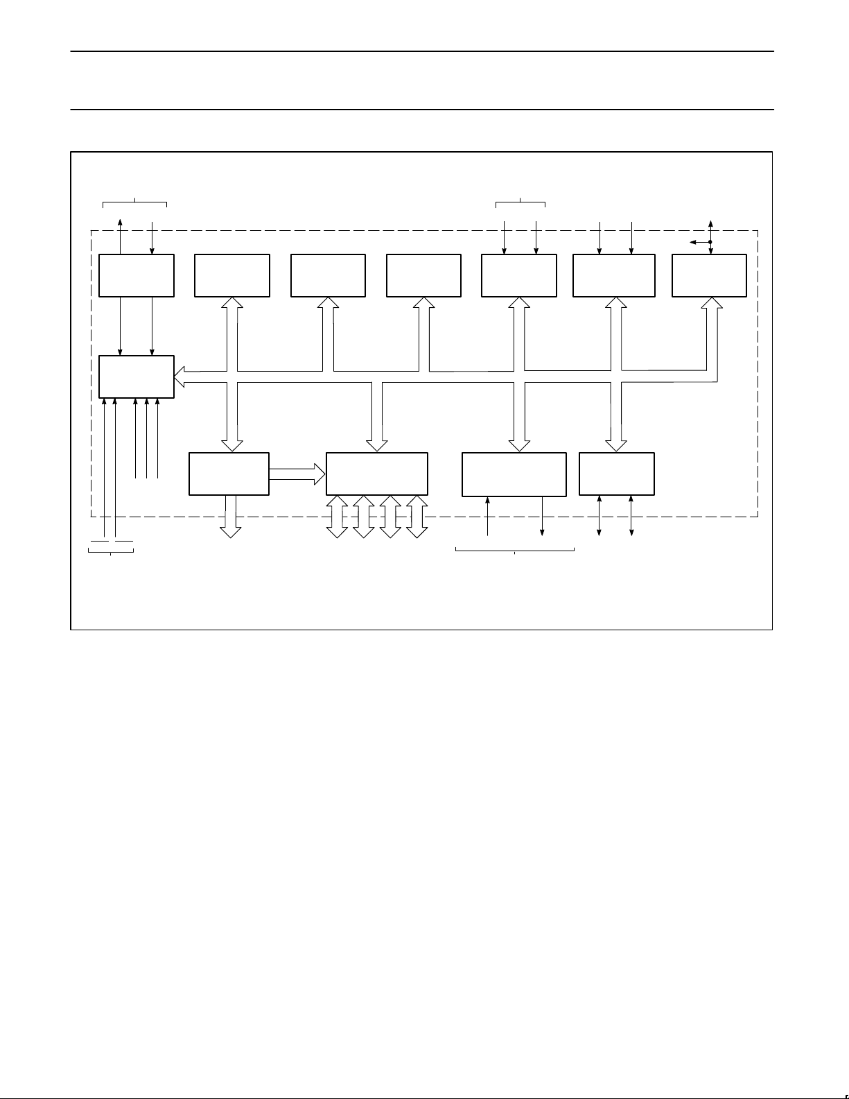
FREQUENCY
REFERENCE
XTAL2 XTAL1
COUNTERS
T0 T1
T2 T2EX
RST
OSCILLATOR
AND
TIMING
INTERNAL
INTERRUPTS
INT1
INT0
EXTERNAL
INTERRUPTS
CPU
PROGRAM
MEMORY
(16K x 8 ROM/
EPROM)
64K-BYTE BUS
EXPANSION
CONTROL
CONTROL
RAM AUX–RAM
DATA
MEMORY
(256 x 8 RAM)
PROGRAMMABLE I/O
PARALLEL PORTS,
ADDRESS/DATA BUS
AND I/O PINS
(256 x 8 RAM)
Figure 1. Block Diagram
DATA
MEMORY
P83C524
TWO 16-BIT
TIMER/EVENT
COUNTERS
PROGRAMMABLE
SERIAL PORT
FULL DUPLEX UART
SYNCHRONOUS SHIFT
SERIAL IN SERIAL OUT
SHARED WITH
PORT 3
16-BIT
TIMER
BIT-LEVEL
2
C
I
INTERFACE
SDA SCL
WATCHDOG
TIMER
1996 Aug 01
3
Philips Semiconductors Short Form Preliminary specification
P83C5248-bit microcontroller
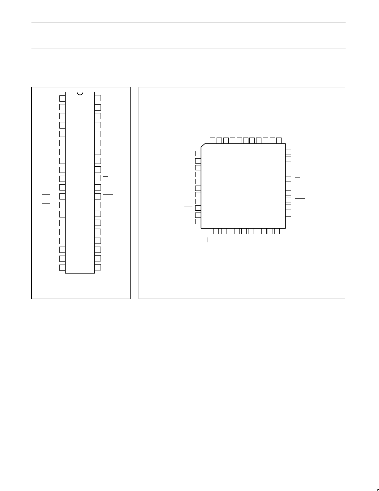
PINNING INFORMATION
Pinning
T2/P1.0
T2EX/P1.1
P1.2
P1.3
P1.4
P1.5
SCL/P1.6
SDA/P1.7
RST
RxD/data/P3.0
TxD/clock/P3.1
/P3.2
INT0
INT1/P3.3
T0/P3.4
T1/P3.5
/P3.6
WR
/P3.7
RD
XTAL2
XTAL1
V
SS
1
2
3
4
5
6
7
8
9
10
11
12
13
14
15
16
17
18
19
20
DUAL
IN-LINE
PACKAGE
40
39
38
37
36
35
34
33
32
31
30
29
28
27
26
25
24
23
22
21
V
DD
P0.0/AD0
P0.1/AD1
P0.2/AD2
P0.3/AD3
P0.4/AD4
P0.5/AD5
P0.6/AD6
P0.7/AD7
EA
ALE
PSEN
P2.7/A15
P2.6/A14
P2.5/A13
P2.4/A12
P2.3/A11
P2.2/A10
P2.1/A9
P2.0/A8
7
P1.5
RST
NC*
P3.4/T0
P3.5/T1
8
9
10
11
12
13
14
15
16
17
P1.6/SCL
P1.7/SDA
P3.0/RXD/data
P3.1/TXD/clock
P3.2/INT0
P3.3/INT1
* DO NOT CONNECT
DD
V
P1.4
P1.3
P1.2
456
18 19 20 21 22 23 24 25 26
XTAL2
P3.7/RD
P3.6/WR
NC*
P1.1/T2EX
P1.0/T2
14443424140
23
PLASTIC
LEADED CHIP
CARRIER
SS
NC*
V
XTAL1
P2.0/A8
P0.0/AD0
P2.1/A9
P0.1/AD1
P0.2/AD2
2827
P2.3/A11
P2.2/A10
P0.3/AD3
39
38
37
36
35
34
33
32
31
30
29
P2.4/A12
P0.4/AD4
P0.5/AD5
P0.6/AD6
P0.7/AD7
EA
NC*
ALE
PSEN
P2.7/A15
P2.6/A14
P2.5/A13
Figure 2. Pin Configuration:
40-lead DIL; (SOT129–1)
Figure 3. Pin Configuration:
44-lead PLCC; (SOT187-2)
1996 Aug 01
4
Philips Semiconductors Short Form Preliminary specification
P83C5248-bit microcontroller
PIN DESCRIPTION
PIN NO.
MNEMONIC DIP PLCC TYPE NAME AND FUNCTION
P1.0–P1.7 1–8 2–9
(1 NC)
1 2 I T2 (P1.0): Timer/event counter 2 external event counter input (falling edge triggered).
2 3 I T2EX (P1.1): T imer/event counter 2 capture/reload trigger or external interrupt 2 input (falling edge
7 8 I/O SCL (P1.6): I2C serial port clock line.
8 9 I/O SDA (P1.7): I2C serial port data line.
RST 9 10 I/O Reset: A HIGH level on this pin for two machine cycles while the oscillator is running, resets the
P3.0–P3.7 10–17 11,
13–19
(12 NC)
10 11 I RxD/data (P3.0): Serial Port data input (asynchonous) or data input/output (synchronous).
11 13 O TxD/clock (P3.1): Serial Port data output (asynchronous) or clock output (synchronous).
12 14 I INT0 (P3.2): External interrupt 0 or gate control input for timer/event counter 0.
13 15 I INT1 (P3.3): External interrupt 1 or gate control input for timer/event counter 1.
14 16 I T0 (P3.4): External input for timer/event counter 0.
15 17 I T1 (P3.5): External input for timer/event counter 1.
16 18 O WR (P3.6): External data memory write strobe.
17 19 O RD (P3.7): External data memory read strobe.
XTAL2 18 20 O Crystal input 2: Output of the inverting amplifier that forms the oscillator. This pin left open-circuit
XTAL1 19 21 I Crystal input 1: Input to the inverting amplifier that forms the oscillator, and input to the internal
V
SS
P2.0–P2.7
(A8 to A15)
20 22 I Ground: Circuit ground potential.
21–28 24–31
(23 NC)
PSEN 29 32 O Program Store Enable output: Read strobe to external program memory via Port 0 and Port 2. It
ALE 30 33 I/O Address Latch Enable output: Latches the LOW byte of the address during access to external
EA 31 35
(34 NC)
P0.0–0.7
32–39 36–43 I/O Port 0: 8-bit open drain bidirectional I/O Port. It is also the multiplexed low-order address and data
(AD0 to
AD7)
V
DD
40 44 I Power Supply: +5V power supply pin during normal operation, Idle mode and Power-down mode.
NC – 1, 12,
23, 34
I/O Port 1: 8-bit quasi-bidirectional I/O port. Port 1 can sink/source one TTL (4 LS TTL) input. It can
drive CMOS inputs without external pull-ups, except P1.6 and P1.7 which have open drain outputs.
Port 1 alternative functions:
triggered)
device. An internal pull-down resistor permits power-on reset using only a capacitor connected to
V
. After a WDT overflow, this pin is pulled HIGH while the internal reset signal is active.
DD
I/O Port 3: 8-bit quasi-bidirectional I/O port with internal pull-ups. Port 3 can sink/source one TTL (=4
LS TTL) input. It can drive CMOS inputs without external pull-ups.
Port 3 alternative functions:
The generation or use of a Port 3 pin as an alternative function is carried out automatically by the
P83C524 provided the associated Special Function Register (SFR) bit is set HIGH.
when an external oscillator clock is used.
clock generator. Receives the external oscillator clock signal when an external oscillator is used.
I/O Port 2: 8-bit quasi-bidirectional I/O port with internal pull-ups. During access to external memories
(RAM/ROM) that use 16-bit addresses (MOVX @DPTR) Port 2 emits the high-order address byte
(A8 to A15). Port 2 can sink/source one TTL (=4 LS TTL) input. It can drive CMOS inputs without
external pull-ups.
is activated twice each machine cycle during fetches from external program memory. When
executing out of external program memory two activations of PSEN
access to external data memory. PSEN
external program memory. PSEN
is not activated (remains HIGH) during fetches from
can sink source 8 LS TTL inputs. It can drive CMOS inputs
are skipped during each
without external pull-ups.
memory in normal operation. It is activated every six oscillator periods except during an external
data memory access. ALE can sink/source 8 LS TTL inputs. It can drive CMOS inputs without an
external pull-up.
I External Access input: When during RESET, EA is held at a TTL HIGH level, the CPU executes
out of the internal program ROM, provided the program counter is less than 32768. When EA
is
held at a TTL LOW level during RESET, the CPU executes out of external program memory via
Port 0 and Port 2. EA
is not allowed to float.
bus during accesses to external memory (AD0 to AD7). During these accesses internal pull-ups are
activated. Port 0 can sink/source 8 LS TTL inputs.
To avoid a “latch-up” effect at power-on, the voltage on any pin (at any time) must not be higher
than V
+0.5V or lower than VSS –0.5V respectively.
DD
– No connection (PLCC only).
1996 Aug 01
5
Philips Semiconductors Short Form Preliminary specification
P83C5248-bit microcontroller
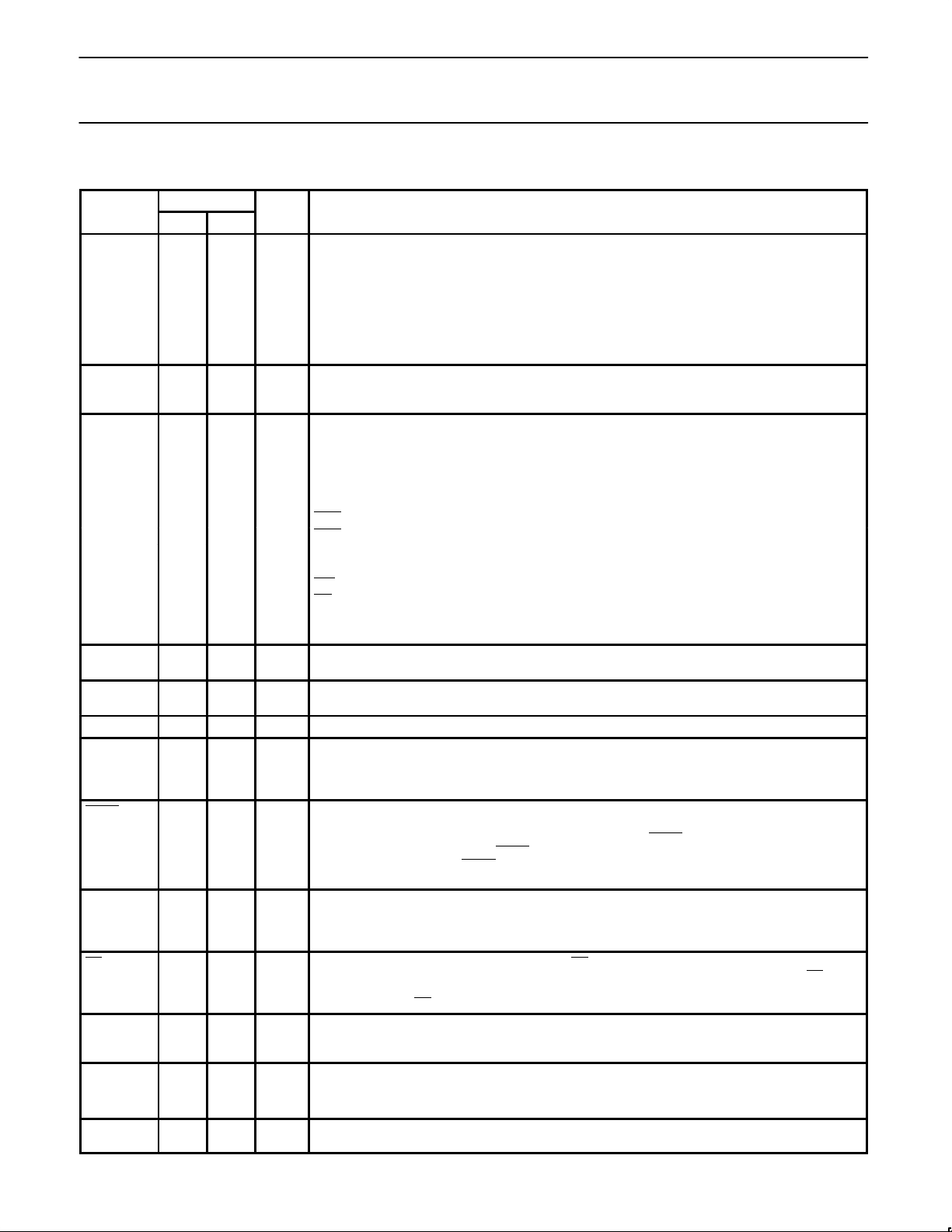
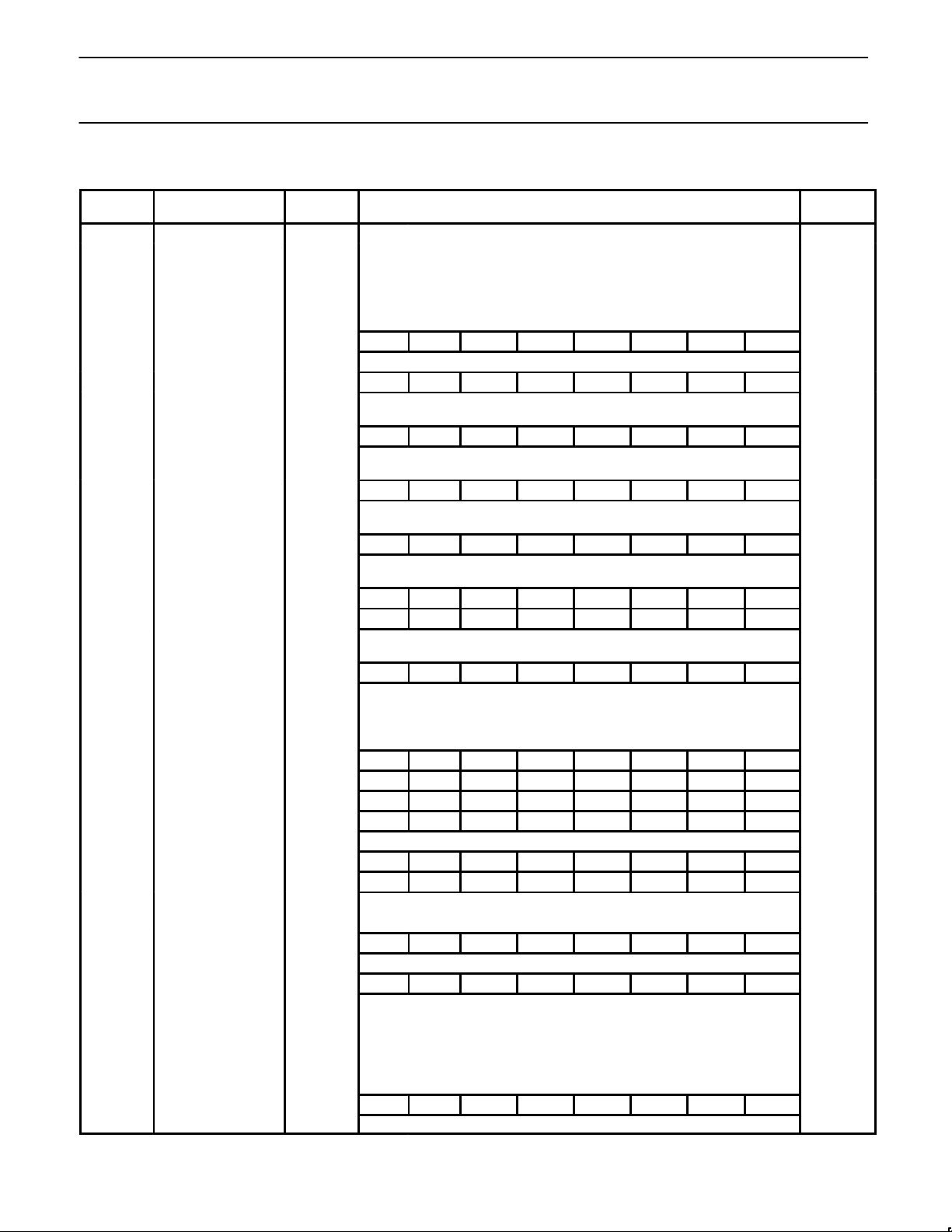
T able 1. 8XC524/8XC528 Special Function Registers
SYMBOL DESCRIPTION
ACC* Accumulator E0H E7 E6 E5 E4 E3 E2 E1 E0 00H
B* B register F0H F7 F6 F5 F4 F3 F2 F1 F0 00H
DPTR:
DPH
DPL
IE*# Interrupt enable A8H EA ES1 ET2 ES0 ET1 EX1 ET0 EX0 00H
IP*# Interrupt priority B8H – PS1 PT2 PS0 PT1 PX1 PT0 PX0 x0000000B
P0* Port 0 80H AD7 AD6 AD5 AD4 AD3 AD2 AD1 AD0 FFH
P1* Port 1 90H SDA SCL – – – – T2EX T2 FFH
Data pointer (2 bytes):
Data pointer high
Data pointer low
DIRECT
ADDRESS
83H
82H
BIT ADDRESS, SYMBOL, OR ALTERNATIVE PORT FUNCTION
MSB LSB
AF AE AD AC AB AA A9 A8
BF BE BD BC BB BA B9 B8
87 86 85 84 83 82 81 80
97 96 95 94 93 92 91 90
RESET
VALUE
00H
00H
A7 A6 A5 A4 A3 A2 A1 A0
P2* Port 2 A0H A15 A14 A13 A12 A11 A10 A9 A8 FFH
B7 B6 B5 B4 B3 B2 B1 B0
P3* Port 3 B0H RD WR T1 T0 INT1 INT0 TxD RxD FFH
PCON Power control 87H SMOD – – – GF1 GF0 PD IDL 0xxx0000B
D7 D6 D5 D4 D3 D2 D1 D0
PSW* Program status word D0H CY AC F0 RS1 RS0 OV F1 P 00H
RCAP2H#
RCAP2L#
SBUF
SCON* Serial controller 98H SM0 SM1 SM2 REN TB8 RB8 TI RI 00H
S1BIT# Serial I2C data D9H/RD SDI 0 0 0 0 0 0 0 x0000000B
S1INT# Serial I2C interrupt DAH INT X X X X X X X 0xxxxxxxB
S1SCS*# Serial I2C control D8H/RD SDI SCI CLH BB RBF WBF STR ENS xxxx0000B
SP Stack pointer 81H 07H
TCON* Timer control 88H TF1 TR1 TF0 TR0 IE1 IT1 IE0 IT0 00H
T2CON*# Timer 2 control C8H TF2 EXF2 RCLK TCLK EXEN2 TR2 C/T2
TH0
TH1
TH2#
TL0
TL1
TL2#
T3#
TMOD Timer mode 89H GATE C/T M1 M0 GATE C/T M1 M0 00H
WDCON# Watchdog control A5H A5H
* SFRs are bit addressable.
# SFRs are modified from or added to the 80C51 SFRs.
Capture high
Capture low
Serial data buffer
Timer high 0
Timer high 1
Timer high 2
Timer low 0
Timer low 1
Timer low 2
Watchdog timer
CBH
CAH
99H
9F 9E 9D 9C 9B 9A 99 98
WR SD0 X X X X X X X 0xxxxxxxB
DF DE DD DC DB DA D9 D8
WR SD0 SC0 CLH X X X STR ENS 00xxxx00B
8F 8E 8D 8C 8B 8A 89 88
CF CE CD CC CB CA C9 C8
CP/RL2
8CH
8DH
CDH
8AH
8BH
CCH
FFH
00H
00H
xxxxxxxxB
00H
00H
00H
00H
00H
00H
00H
00H
1996 Aug 01
6
Philips Semiconductors Short Form Preliminary specification
P83C5248-bit microcontroller
Table 2. Internal and External Program Memory Access with Security Bit Set
INSTRUCTION
ACCESS TO INTERNAL
PROGRAM MEMORY
MOVC in internal program memory YES YES
MOVC in external program memory NO YES
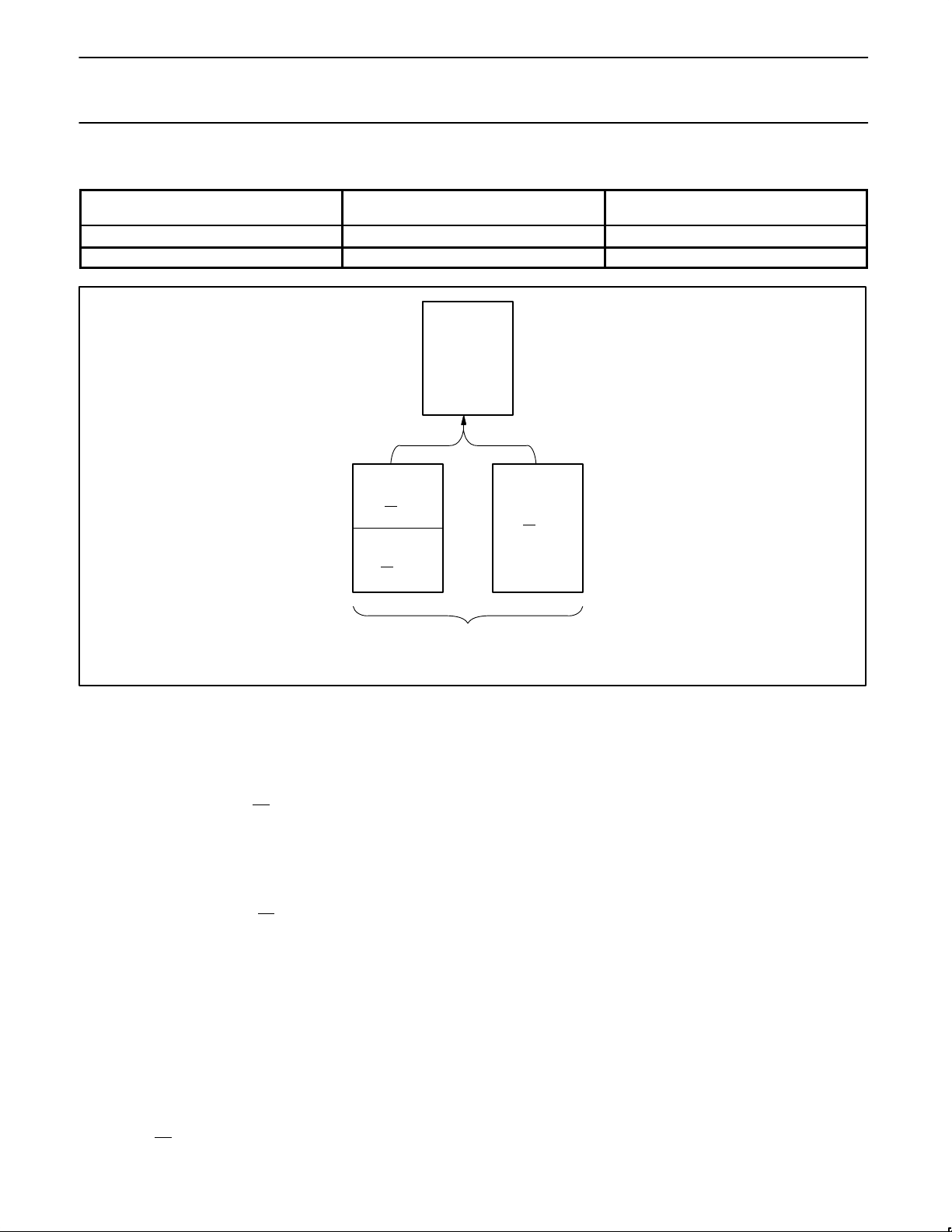
64 K
External
32768
32767
32767
Internal
not useable
(EA
16384
16383
0 0
= 1)
Internal
useable
(EA
= 1)
External
= 0)
(EA
ACCESS TO EXTERNAL
PROGRAM MEMORY
PROGRAM MEMORY
The program memory address space of the
P83C524 comprises an internal and an
external memory portion. The P83C524 has
16 kbyte of usable program memory on–chip.
The program memory can be externally
expanded up to 64 kbyte. If the EA
pin is held
HIGH during RESET, the P83C524 executes
out of the internal program memory unless
the address exceeds 32767 (notice: Only
address 0 to 16383 of the internal program
memory can be used). Locations 32768
through 64K are then fetched from the
external program memory. If the EA
pin is
held LOW during RESET, the P83C524
fetches all instructions from the external
program memory . Figure 4 illustrates the
program memory address space.
ROM CODE PROTECTION
By setting a mask programmable security bit,
the ROM content in the 83C524 is protected,
i.e., it cannot be read out by any test mode or
by any instruction in the external program
memory space. The MOVC instructions are
the only ones which have access to program
code in the internal or external program
memory. The EA
RESET and is ‘don’t care’ after RESET (also
input is latched during
Program Memory
Figure 4. Program Memory Address Space.
if security bit is not set). This implementation
prevents reading from internal program code
by switching from external program memory
to internal program memory during MOVC
instruction or an instruction that handles
immediate data. Table NO TAG lists the
access to the internal and external program
memory by the MOVC instructions when the
security bit has been set to logical one. If the
security bit has been set to a logical 0 there
are no restrictions for the MOVC instructions.
INTERNAL DATA MEMORY
The internal data memory is divided into
three physically separated segments: 256
bytes of RAM, 256 bytes of AUX-RAM, and a
128 bytes special function area. These can
be addressed each in a different way .
– RAM 0 to 127 can be addressed directly
and indirectly as in the 80C51. Address
pointers are R0 and R1 of the selected
register bank.
– RAM 128 to 255 can only be addressed
indirectly as in the 80C51. Address
pointers are R0 and R1 of the selected
register bank.
– AUX-RAM 0 to 255 is indirectly addressed
in the same way as external data memory
with the MOVX instructions. Address
pointers are R0, R1 of the selected register
bank and DPTR. An access to AUX-RAM 0
to 255 will not affect ports P0, P2, P3.6 and
P3.7.
An access to external data memory locations
higher than 255 will be performed with the
MOVX DPTR instructions in the same way as
in the 8051 structure, so with P0 and P2 as
data/address bus and P3.6 and P3.7 as write
and read timing signals. Note that these
external data memory cannot be accessed
with R0 and R1 as address pointer.
TIMER 2
Timer 2 is functionally equal to the Timer 2 of
the 8052AH. Timer 2 is a 16-bit timer/counter .
These 16 bits are formed by two special
function registers TL2 and TH2. Another pair
of special function register RCAP2L and
RCAP2H form a 16-bit capture register or a
16-bit reload register. Like Timer 0 and 1, it
can operate either as a timer or as an event
counter. This is selected by bit C/T2N in the
special function register T2CON. It has three
operating modes: capture, autoload, and
baud rate generator mode which are selected
by bits in T2CON.
1996 Aug 01
7

Philips Semiconductors Short Form Preliminary specification
P83C5248-bit microcontroller
WATCHDOG TIMER T3
The watchdog timer (WDT) (see Figure 5)
consists of an 11-bit prescaler and an 8-bit
timer formed by special function register T3.
The prescaler is incremented by an on-chip
oscillator with a fixed frequency of 1MHz. The
maximum tolerance on this frequency is
–50% and +100%. The 8-bit timer increments
every 2048 cycles of the on-chip oscillator.
When a timer overflow occurs, the
microcontroller is reset and a reset output
pulse of 16 × 2048 cycles of the on-chip
oscillator is generated at pin RST. The
internal RESET signal is not inhibited when
the external RST pin is kept LOW by, for
example, an external reset circuit. The
RESET signal drives Ports 1, 2 and 3 outputs
into the HIGH state and port 0 into high
impedance, whether the XTAL-clock is
running or not.
The watchdog timer is controlled by special
function register WDCON with the direct
address location A5H. WDCON can be read
and written by software. A value of A5H in
WDCON halts the on-chip oscillator and
clears both the prescaler and timer T3. After
the RESET signal, WDCON contains A5H.
Every value other than A5H in WDCON
enables the watchdog timer. When the
watchdog timer is enabled, it runs
independently of the XTAL-clock.
Timer T3 can be read on the fly. Timer T3 can
be written to only if WDCON has previously
been loaded with 5AH, otherwise T# and the
prescaler are not affected. A successful write
operation to T3 also clears the prescaler and
WDCON. During a read or write operation
addressing T3, the output of the on-chip
oscillator is inhibited to prevent timing
problems due to asynchronous increments of
T3. To prevent an overflow of the watchdog
timer, the user program has to reload T3
within periods that are shorter than the
programmed watchdog timer internal. This
time interval is determined by the 8-bit reload
value that is written into register T3.
Watchdog timer interval =
[256 (T3)] 2048
on chip oscillator frequency
The advantages of this implementation are:
•Only an internal reset connection to the
microcontroller core.
•The Power-down mode and the Watchdog
(WDT) function can be used concurrently.
•The WDT also monitors the XTAL
oscillator. In case of a failure the port
outputs are forced to a defined HIGH state.
•Interference will not disable the WDT
because it is unlikely that it will force
WDCON to A5H.
•Tolerances of the on-chip oscillator can be
adjusted by testing the T3 value and
adapting the reload value.
•The WDT can be enabled and disabled
under control of the user software. This
gives the possibility to use both the
Watchdog function and the Power-down
function.
•The direct address A5H of WDCON and its
disable value A5H will not unintentionally
be present at a random location in the field
of program code, except for immediate
data, because the opcode A5H is not used
in the instruction set.
1996 Aug 01
Figure 5. Watchdog Timer T3
8
Philips Semiconductors Short Form Preliminary specification
P83C5248-bit microcontroller
BIT-LEVEL I2C INTERFACE
This bit-level serial I/O interface supports the
2
I
C-bus (see Figure 6). P1.6/SCL and
P1.7/SDA are the serial I/O pins. These two
pins meet the I
the input levels and output drive capability.
Consequently , these pins have an open drain
output configuration. All the four modes of the
2
I
C-bus are supported:
– master transmitter
– master receiver
– slave transmitter
– slave receiver
The advantages of the bit-level I
compared with a full software I
implementation are:
– The hardware can generate the SCL pulse
– Testing a single bit (RBF respectively,
WBF) is sufficient as a check for error free
transmission.
The bit-level I
bit level and performs the following functions:
– filtering the incoming serial data and clock
signals
– recognizing the START condition
– generating a serial interrupt request SI
after reception of a STAR T condition and
the first falling edge of the serial clock
– recognizing the STOP condition
– recognizing a serial clock pulse on the SCL
line
– latching a serial bit on the SDA line (SDI)
2
C specification concerning
2
C hardware
2
C
2
C hardware operates on serial
– stretching the SCL LOW period of the
serial clock to suspend the transfer of the
next serial data bit
– setting Read Bit Finished (RBF) when the
SCL clock pulse has finished and Write Bit
Finished (WBF) if there is no arbitration
loss detected (i.e., SDA = 0 while SDO = 1)
– setting a serial clock Low-to-High detected
(CLH) flag
– setting a Bus Busy (BB) flag on a START
condition and clearing this flag on a STOP
condition
– releasing the SCL line and clearing the
CLH, RBF and WBF flags to resume
transfer of the next serial data bit
– generating an automatic clock if the single
bit data register S1BIT is used in master
mode.
The following functions must be done in
software:
– handling the I
2
C START interrupts
– converting serial to parallel data when
receiving
– converting parallel to serial data when
transmitting
– comparing the received slave address with
its own
– interpreting the acknowledge information
– guarding the I
2
C status if RBF or WBF = 0.
Additionally, if acting as master:
– generating START and ST OP conditions
– handling bus arbitration
– generating serial clock pulses if S1BIT is
not used.
Three SFRs control the bit-level I2C interface:
S1INT, S1BIT and S1SCS.
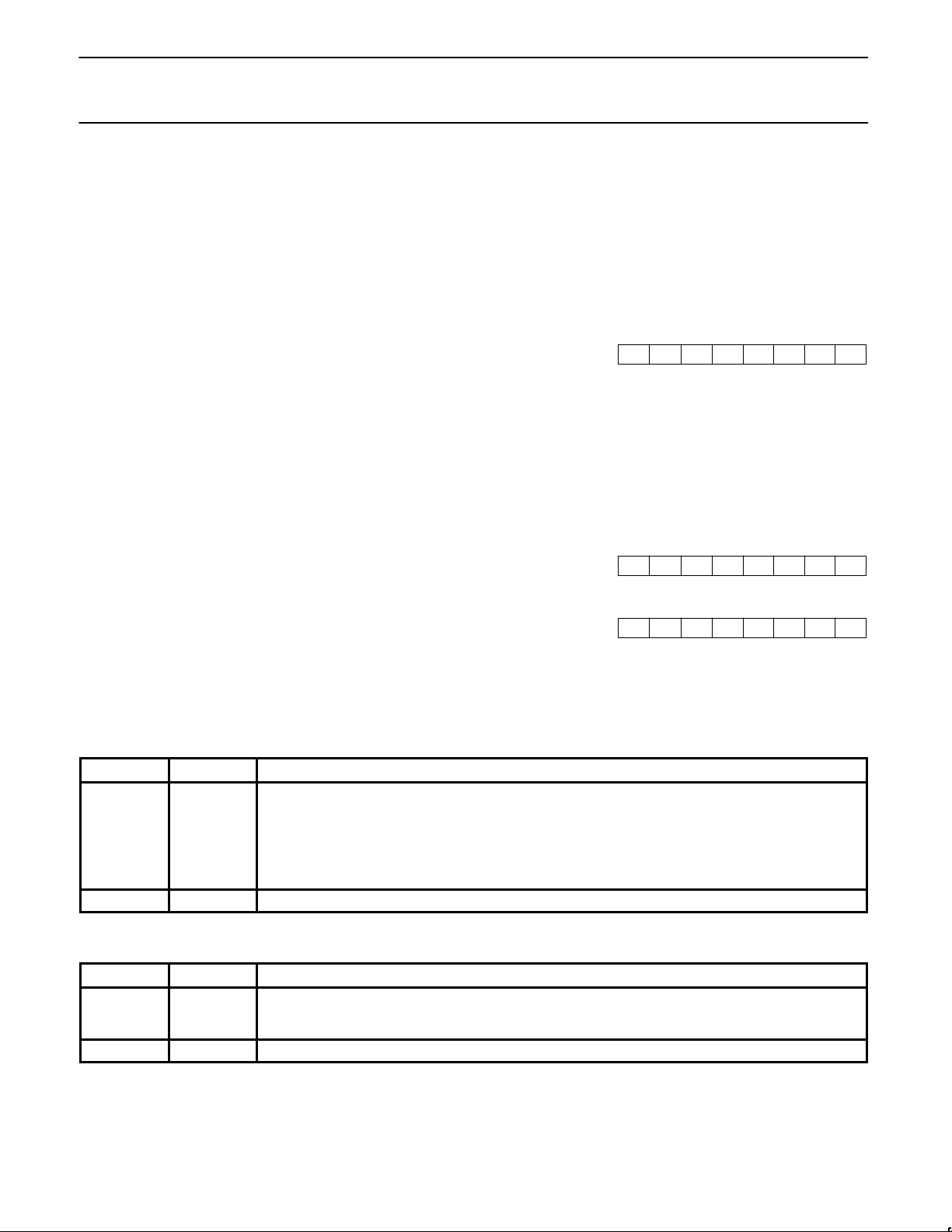
S1INT: I2C Interrupt Register
This register is located at address DAH.
Refer to Table 1.
S1INT SFR (DAH)
7 6 543210
XXXXSI X X X
NOTE:
1. SI bit: Writing a logic 0 clears this bit,
writing a logic 1 has no effect.
S1BIT: Single-bit Data Register
2
with I
This register is located at address D9H.
Refer to Table 2.
S1BIT SFR (D9H)
READ
WRITE
NOTE:
1. Access of the S1BIT SFR clears SI, CLH,
C Auto-Clock
7 6 543210
0000SDI 0 0 0
7 6 543210
XXXXSDO X X X
RBF and WBF. It starts the auto-clock if
SCO = 0.
Table 1. Description of S1INT Bits
MNEMONIC BIT FUNCTION
SI S1INT.7 Serial Interrupt request (SI) flag: If a START condition occurs the SI flag in the S1INT SFR is set on the
falling edge of the filtered serial clock. If SI = 1 is detected during a transfer this can be a “spurious STAR T”
error condition. If no transfer is taking place the SI = 1 is a STAR T from an external master. Provided the bits
EA and ES1 in IE SFR are set, SI then generates an interrupt so that a slave address receive routine can be
started. SI can be cleared by accessing the S1BIT register or by writing “00” to S1INT. Also after reception of
a STAR T condition, the LOW period of the clock pulse is stretched, suspending the serial transfer to allow
the software to take action. This clock stretching is ended by a read or write access to S1BIT.
– S1INT.6 to 0 X = undefined during read, don’t care during write.
Table 2. Description of S1BIT Bits
MNEMONIC BIT FUNCTION
SDO/SDI S1BIT.7 Serial Data Output (SDO) and the filtered Serial Data Input (SDI). SDI data is latched on the rising edge
– S1BIT.6 to 0 X = don’t care.
of the filtered serial clock. S1BIT.7 accesses the same memory locations as S1SCS.7. S1BIT SFR is not
bit-addressable.
1996 Aug 01
9
 Loading...