

Philips p83c434 834 DATASHEETS

INTEGRATED CIRCUITS
DATA SH EET
P83C434; P83C834
8-bit microcontrollers with
LCD-driver
Product specification
Supersedes data of 1996 Oct 16
File under Integrated Circuits, IC20
1997 Jul 03

Philips Semiconductors Product specification
8-bit microcontrollers with LCD-driver P83C434; P83C834
CONTENTS
1 FEATURES
1.1 Differences from the 80C51 core
1.2 Memory
2 GENERAL DESCRIPTION
3 ORDERING INFORMATION
4 BLOCK DIAGRAM
5 PINNING INFORMATION
5.1 Pinning
5.2 Pin description
6 FUNCTIONAL DESCRIPTION
6.1 Input/Output (I/O)
6.2 Oscillator
6.3 Interrupts
6.4 Reduced power modes
6.5 Reset
6.6 Special Function Registers (SFRs)
6.7 LCD driver unit
7 LIMITING VALUES
8 HANDLING
9 DC CHARACTERISTICS
10 LCD DRIVER CHARACTERISTICS
11 AC CHARACTERISTICS
11.1 Characteristic curves
12 APPLICATION INFORMATION
13 PACKAGE OUTLINE
14 SOLDERING
14.1 Introduction
14.2 SDIP
14.3 QFP
15 DEFINITIONS
16 LIFE SUPPORT APPLICATIONS
1997 Jul 03 2

Philips Semiconductors Product specification
8-bit microcontrollers with LCD-driver P83C434; P83C834
1 FEATURES
• 80C51 type core
• System clock derived from an internal free running
Current Controlled Oscillator (CCO); no external
components required. Clock frequency can be adjusted
by software.
• Optimized for EMC (Electromagnetic Compatibility)
• Clock frequency f
• 12 I/O lines, quasi-bidirectional
• Gated interrupt on 8 I/O lines:
– P0.0 to P0.3 when LOW
– P0.4 to P0.7 when LOW or HIGH
• LCD driver clock, 32 kHz, which also provides the time
base for a Real Time Clock
• 1-second interrupt by internal 15-bit counter
• On-chip Liquid Crystal Display (LCD) drivers with
26 outputs, comprising:
– 22, 23 or 24 segment drivers
– 1 to 4 backplanes
• LCD multiplexing rates: 1 : 1 (static), 1 : 2, 1 : 3 or 1 : 4
• Operating temperature: −40 to +85 °C
• Single power supply:
– Operating voltage: 3.5 to 5.5 V
– Power-down mode: 1.8 V.
= 1 to 12 MHz
clk
• Timer 0 external input replaced by a direct connection to
the 32 kHz oscillator output.
• Timer 1 external input is connected to pin P0.0 (Port 0);
alternate function of P0.0.
• Standard serial interface and its control register is not
present.
• Adjustable on-chip oscillator without external
components.
• Wake-up from Power-down mode is also possible by
means of an interrupt.
• Extended external interrupts.
1.2 Memory
Table 1 ROM/RAM sizes
MEMORY
DEVICE
ROM RAM
P83C434 4 kbytes 128 bytes
P83C834 8 kbytes 256 bytes
2 GENERAL DESCRIPTION
The P83C434 and P83C834 are low-cost microcontrollers
of the 80C51 family, with LCD drivers.
Main application is in the user-interface (keypad, display)
of consumer products, e.g. portable radios, CD-players,
etc.
1.1 Differences from the 80C51 core
• Port 0 quasi-bidirectional instead of open-drain.
• No external memory connection.
Signals
• Port 1, Port 2 (pins P2.4 to P2.7) and Port 3 are not
present.
3 ORDERING INFORMATION
P83C434CFP;
P83C834CFP
1997 Jul 03 3
EA, ALE and PSEN are not present.
PACKAGE
TYPE NUMBER
NAME DESCRIPTION VERSION
SDIP42 plastic shrink dual in-line package; 42 leads (600 mil) SOT270-1 −40 to +85
QFP44 plastic quad flat package; 44 leads (lead length 1.3 mm);
body 10 × 10 × 1.75 mm
This data sheet details the specific properties of the
P83C434 and P83C834. The shared characteristics of the
80C51 family of microcontrollers are described in
Handbook IC20”
this data sheet.
, which should be read in conjunction with
SOT307-2
“Data
TEMP.
RANGE (°C)
Philips Semiconductors Product specification
8-bit microcontrollers with LCD-driver P83C434; P83C834
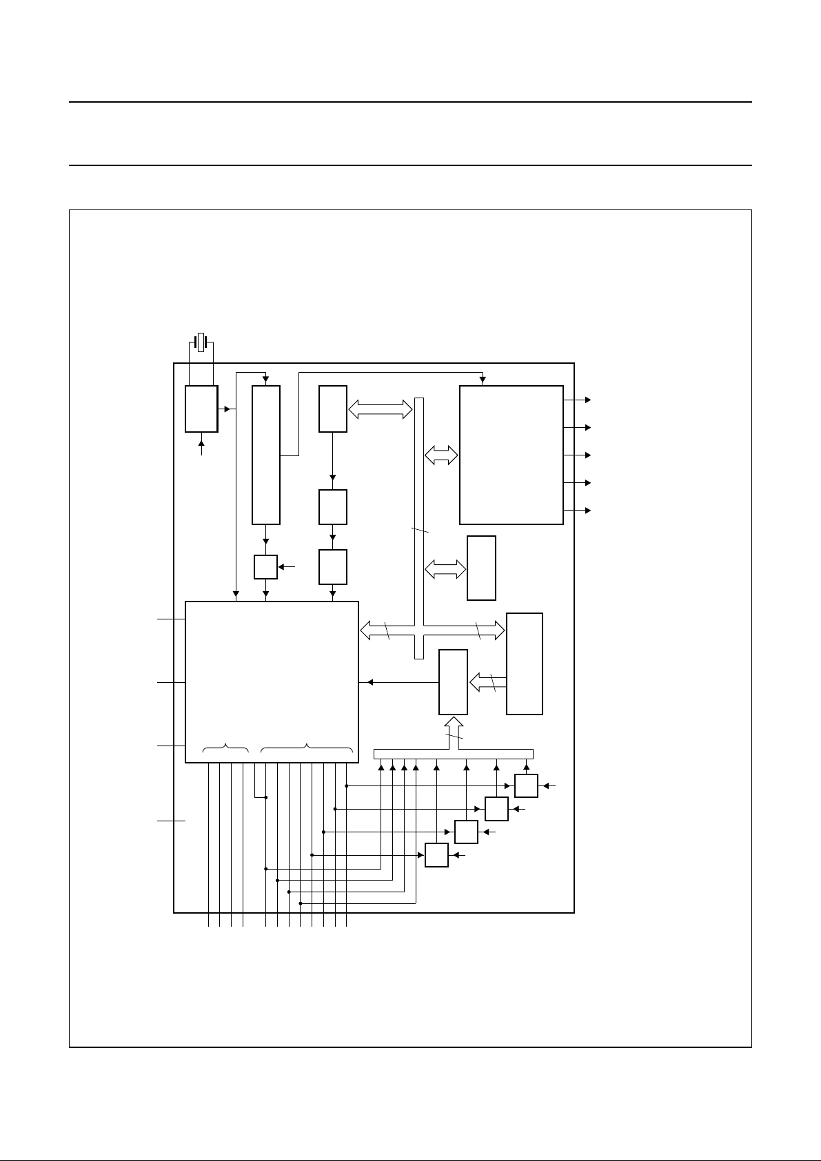
4 BLOCK DIAGRAM
32
kHz
SS
V
RESET
DD(C)
V
XTAL1
XTAL2
OSC
MCON.5
0123T101234567
1-SECOND COUNTER
T0
EI1
80C51 CORE
P2.0 to P2.3
CCO D/A OSCON
MCON.4
CLOCK
P0.0 to P0.7
internal busEI0
MGG012
BP0BP1S23/
CLOCK
S22/
S00toS21
(1)
BP2
BP3
Fig.1 Block diagram.
LCD
internal
8
MCON
8
8
GATES
INTERRUPT
8
UNIT
8
REGISTER (IG).
INTERRUPT GATES
DD(P)
V
P0.7
P0.6
P0.5
P0.4
P0.3
P0.2
P0.1
P0.0
P2.3
P2.2
P2.1
P2.0
handbook, full pagewidth
1997 Jul 03 4
MCON.3
MCON.2
MCON.1
MCON.0
(1) Drive lines S00 and S21 are not available with the SDIP42 (SOT270-1) package.
Philips Semiconductors Product specification
8-bit microcontrollers with LCD-driver P83C434; P83C834
5 PINNING INFORMATION
5.1 Pinning
handbook, halfpage
S23/BP2 S22/BP3
RESET
V
V
BP1
BP0
P2.0
P2.1
P2.2
P2.3
DD(P)
V
SS
DD(C)
XTAL1
XTAL2
P0.0
P0.1
P0.2
P0.3
P0.4
1
2
3
4
5
6
7
8
9
10
11
12
13
14
15
16
17
18
P83C434
P83C834
42
41
S20
S19
40
39
S18
S17
38
37
S16
S15
36
35
S14
S13
34
33
S12
32
S11
31
S10
30
S09
S08
29
28
S07
S06
27
S05
26
S04
25
P0.5
19
P0.6
20
P0.7 S01
21
Fig.2 Pinning diagram for SDIP42 (SOT270-1).
1997 Jul 03 5
MGG011
S03
24
S02
23
22

Philips Semiconductors Product specification
8-bit microcontrollers with LCD-driver P83C434; P83C834
handbook, full pagewidth
P2.1
P2.0
BP0
BP1
S23/BP2
S22/BP3
S21
S20
S19
S18
S17
44
41
40
39
38
43
42
37
363534
P2.2
P2.3
RESET
V
DD(P)
V
V
DD(C)
XTAL1
XTAL2
P0.0
P0.1
P0.2
SS
1
2
3
4
5
14
P0.5
P83C434
P83C834
15
16
P0.6
P0.7
17
S00
18
S01
19
S02
202122
S03
S04
6
7
8
9
10
11
12
13
P0.3
P0.4
S05
33
S16
32
S15
31
S14
30
S13
29
S12
28
S11
27
S10
26
S09
25
S08
24
S07
23
P06
MGG010
Fig.3 Pinning diagram for QFP44 (SOT307-2).
1997 Jul 03 6

Philips Semiconductors Product specification
8-bit microcontrollers with LCD-driver P83C434; P83C834
5.2 Pin description Table 2 Pin description for SDIP42 and QFP44
PIN
SYMBOL
SDIP42
(SOT270-1)
QFP44
(SOT307-2)
S23/BP2 1 40 segment drive line 23/Backplane drive line 2
BP1 2 41 backplane drive line 1
BP0 3 42 backplane drive line 0
P2.0 to P2.3 4 to 7 43, 44, 1 and 2 quasi-bidirectional I/O line
RESET 8 3 reset input
V
DD(P)
V
SS
V
DD(C)
9 4 power supply (+) for periphery and LCD unit; see note 1
10 5 ground; double bonded
11 6 power supply for the core; see note 1
XTAL1 12 7 oscillator, XTAL connections
XTAL2 13 8
P0.0 to P0.7 14 to 21 9 to 16 Port 0: quasi-bidirectional I/O lines
S00 − 17 segment drive line 0; see note 2
S01 to S20 22 to 41 18 to 37 segment drive line 1 to 20
S21 − 38 segment drive line 21; see note 2
S22/BP3 42 39 segment drive line 22/Backplane drive line 3
DESCRIPTION
Notes
1. For proper V
supply to V
DD
DD(P)
and V
see Section 6.1.1.
DD(C)
2. In package SDIP42 (SOT270-1) segment drive lines S00 and S21 are not connected, so the total number of drive
lines is 22.
1997 Jul 03 7
Philips Semiconductors Product specification
8-bit microcontrollers with LCD-driver P83C434; P83C834
6 FUNCTIONAL DESCRIPTION
The block diagram is shown in Fig.1. The P83C434 and
P83C834 provide all functions that are required for a user
interface. This is illustrated in the radio application detailed
in Chapter 12. In the following sections the functions of the
device are described.
6.1 Input/Output (I/O)
A total of 12 I/O lines are available.
Port 0 P0.0 to P0.7 (8 lines).
Port configuration: Quasi-bidirectional (push-pull in
emulation mode). For the Interrupt generation see
Fig.10. If one of the port lines P0.0 to P0.3 is a
logic 0 or one of the port lines P0.4 to P0.7 is equal
to the corresponding bit in the Miscellaneous
Control Register (MCON) and the corresponding bit
in the Interrupt Gate Register (IG) is a logic 1, then
an
INT0 interrupt is generated.
Port 2 P2.0 to P2.3 (4 lines).
Port configuration: Quasi-bidirectional (push-pull in
emulation mode). When writing to Port 2, bits
P2.4 to P2.7 have to be fixed at HIGH. Data to be
written should be ‘1111XXXXB’.
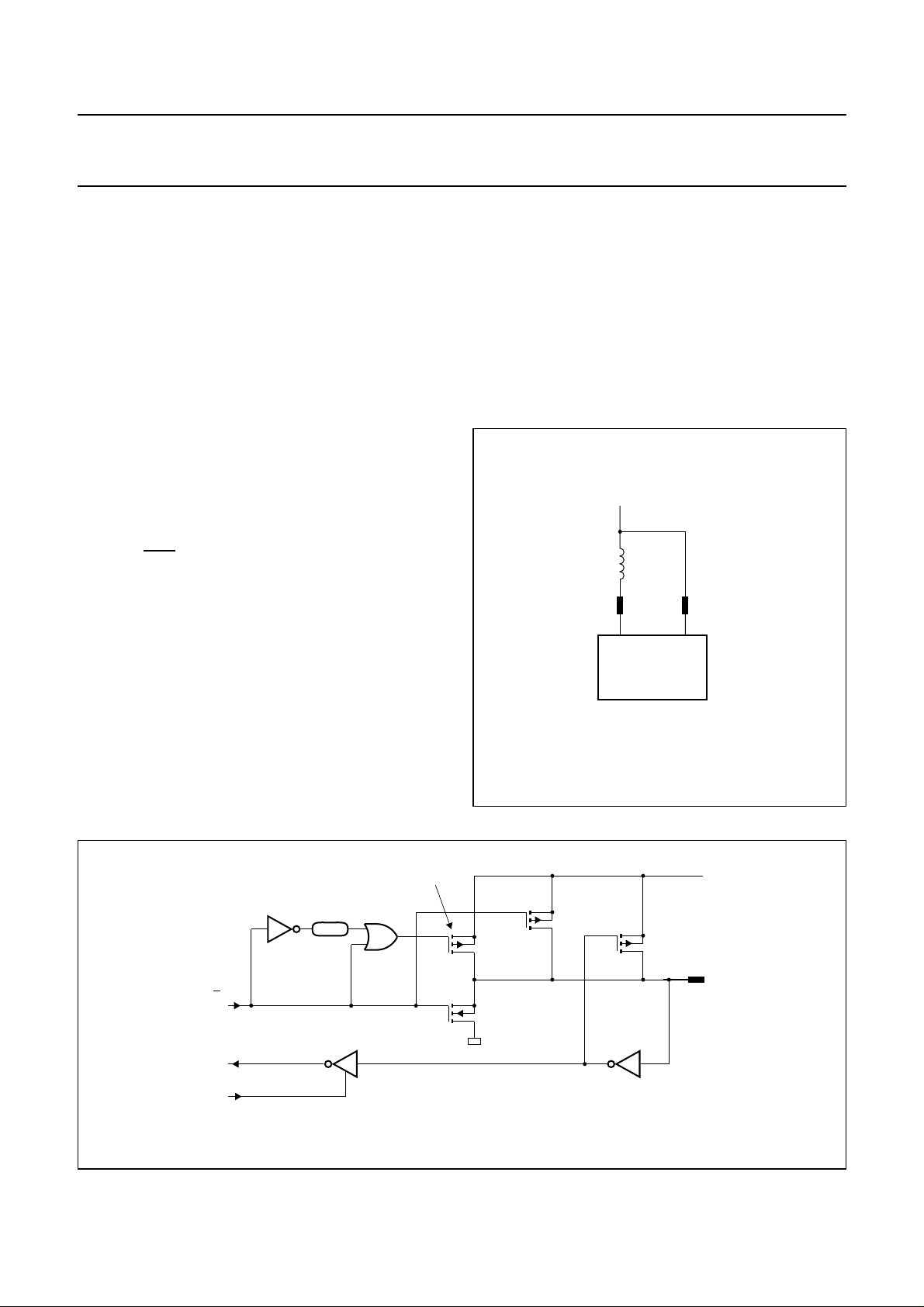
6.1.1 EMC (E
LECTROMAGNETIC COMPATIBILITY)
In order to reduce EMI (Electromagnetic Interference) the
following design measures have been taken:
• Slope control is implemented on all the I/O lines.
Rise and fall time (10% to 90%) are:
20 ns < rise/fall time < 50 ns.
• The power supply and ground pins are placed next to
each other.
• Double bonding V
pins, i.e. 2 bondpads for each pin.
SS
• Limiting the drive capability of:
– clock drivers and prechargers.
– segment drivers and backplane drivers for the LCD.
• External decoupling of the of the CPU supply V
to avoid interference on the VDD line, the V
V
pins should be connected as illustrated in Fig.4.
DD(P)
V
DD(C)
V
DD
2.2 µH
P83C434
P83C834
V
MGG019
DD(P)
andbook, halfpage
DD(C)
DD(C)
and
Fig.4 Avoiding interference on VDD.
;
handbook, full pagewidth
from port latch
read port pin
input data
2 oscillator
periods
Q
strong pull-up
INPUT
BUFFER
Fig.5 Standard output with switched pull-up current source.
1997 Jul 03 8
V
DD
p2
p1
n
p3
I/O PIN
I1
MLC926 - 1
Philips Semiconductors Product specification
8-bit microcontrollers with LCD-driver P83C434; P83C834
6.2 Oscillator
6.2.1 CPU
CLOCK
The internal timing circuits of the CPU are clocked by a
Current Controlled Oscillator (CCO). The oscillator is free
running and is adjusted by means of the Oscillator Control
Register (OSCON; see Section 6.6.4) and a
digital-to-analog converter; it does not require external
components. The frequency of the CPU clock can be
measured by means of Timer T0 which is clocked by the
32 kHz oscillator (see Section 6.2.2).
Adjustments can be made by changing the contents of the
OSCON register (see Fig.9). Over the range 0 to 31 the
frequency step size is constant (deviation ≤10%).
The frequency variation per step of the register is:
0.5 MHz < step size < 2 MHz.
At Power-on-reset the oscillator frequency will be:
1MHz<f
< 4 MHz. Stability of the oscillator:
OSC
frequency change with time ≤1.5%. The maximum
operating frequency is: ≤12 MHz at VDD≥4.5 V.
The minimum operating frequency is 1 MHz.
In Power-down mode the oscillator is stopped.
6.2.2 LCD
DRIVER CLOCK:32KHZ OSCILLATOR
Table 3 Oscillator status during Power-down mode
RUN32 32 kHz OSCILLATOR
HIGH running
LOW stopped
6.2.3 15-
BIT COUNTER (1-SECOND TIMER)
An interrupt is generated every second by the 15-bit
counter. This 1-second timer is a 15-bit counter, clocked
by the 32 kHz oscillator output. When this counter
overflows it generates an INT1 interrupt by setting SECINT
in the Miscellaneous Control Register (MCON). Reset of
this interrupt is carried out via software by clearing bit
SECINT.
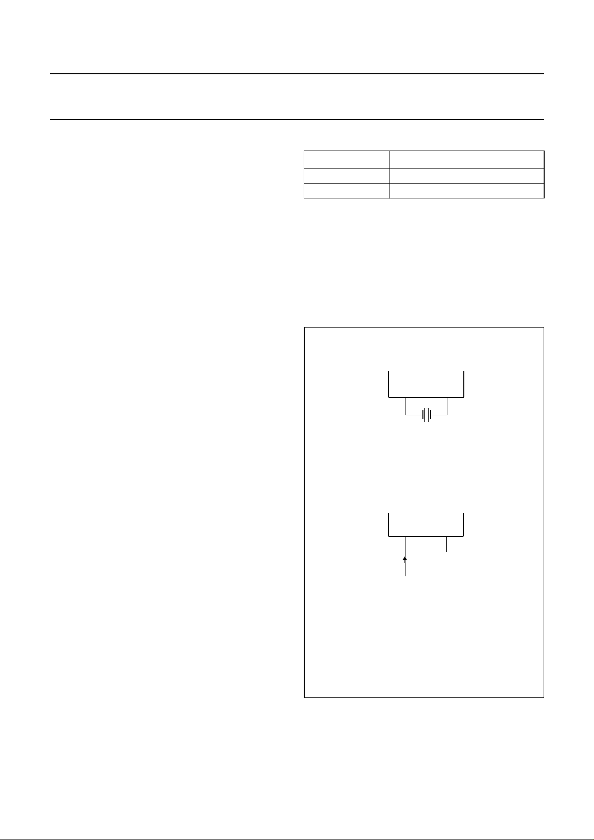
handbook, halfpage
XTAL1 XTAL2
MLC928
A 32 kHz oscillator provides the clocking of the LCD timing
generator and may also be used as the time base for a
Real Time Clock. The output of the 32 kHz oscillator is also
used as an input of Timer/Counter 0.
The frequency of the 32 kHz oscillator need not be exactly
32 kHz, and is determined by the component(s) connected
between pins XTAL1 and XTAL2. See Chapter 11.
The oscillator is suitable for use with either:
• A crystal; connected as shown in Fig.6a
• External drive; connected as shown in Fig.6b.
During Power-down mode, the control bit RUN32 in the
Miscellaneous Control Register (MCON) determines
whether the oscillator is stopped or running continuously;
see Table 3.
The output of the oscillator (XTAL2) is used as an input to
the Timer/Counter 0. This can be useful for accurate time
measurements and generation of time-slots. For example
it may be used to determine (and possibly adjust) the
frequency of the CCO that is used for the CPU clock.
a. Crystal oscillator.
handbook, halfpage
XTAL1 XTAL2
n.c.
external clock
(not TTL compatible)
MBE312
b. External clock drive.
Fig.6 Oscillator configurations P83C434/P83C834.
1997 Jul 03 9
Philips Semiconductors Product specification
8-bit microcontrollers with LCD-driver P83C434; P83C834
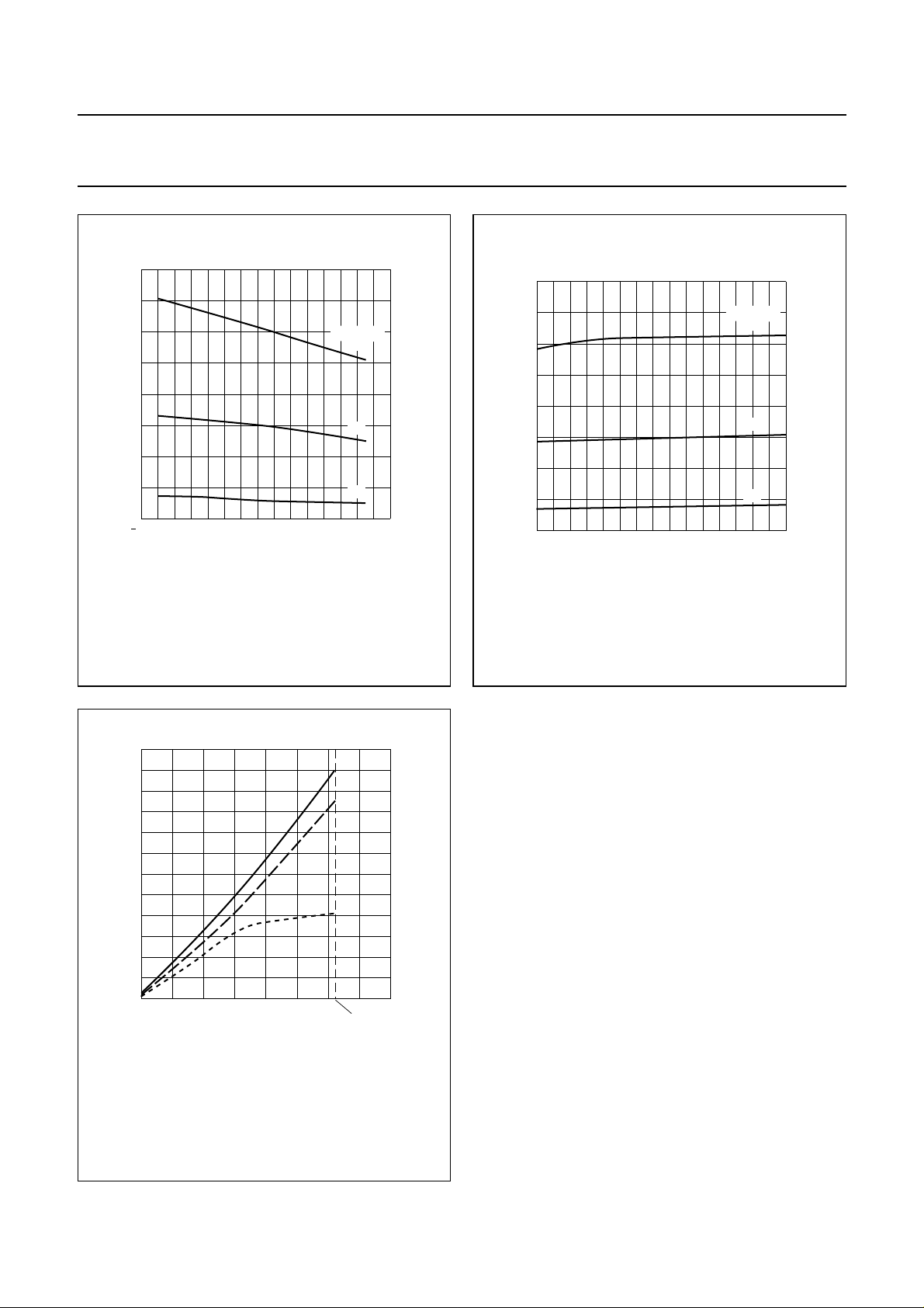
16
handbook, halfpage
f
osc
(MHz)
12
8
4
0
50 0 100
Fig.7 f
at VDD=5V.
50
as function of temperature;
osc
MBE313
OSCON =
FH
7H
1H
o
T ( C)
16
handbook, halfpage
f
osc
(MHz)
12
8
4
0
23 5
Fig.8 f
4
as function of VDD.
osc
MBE314
OSCON =
FH
7H
1H
V (V)
DD
36
handbook, halfpage
f
osc
(MHz)
24
12
0
01020 40
(1) Fast case; VDD= 5.5V, T
(2) Typical case; VDD= 4.0V, T
(3) Slow case; VDD= 2.0V, T
contents of OSCON (decimal)
Fig.9 f
osc
MBE315
(1)
(2)
(3)
30
31(max)
= −40°C.
amb
=25°C.
amb
=85°C.
amb
as function of OSCON.
1997 Jul 03 10

Philips Semiconductors Product specification
8-bit microcontrollers with LCD-driver P83C434; P83C834
6.3 Interrupts
The P83C434 and P83C834 have 4 interrupt sources;
these are shown Fig.10.
Interrupt INT0 is generated when one of the I/O lines
(P0.0 to P0.3) becomes LOW; or one of I/O lines
(P0.4 to P0.7) equals the corresponding bit in the MCON
register (ILVL0 to ILVL3). By means of bit IT0 in the TCON
register this interrupt can be chosen to be:
• Level sensitive, when IT0 = LOW; INT0 must be inactive
before a return from interrupt is given, otherwise the
same interrupt will occur again.
• Edge sensitive, when IT0 = HIGH; the internal hardware
will reset the latch when the LCALL is executed for the
vector address (see Table 7).
Interrupt INT1 is generated by the overflow of the 1-second
counter. The overflow signal is latched. The output of the
latch will set the SECINT bit in the MCON register.
When SECINT is set the overflow latch will be reset.
Interrupt INT1 is selected as edge or level sensitive by the
state of the IT1 bit in the TCON register. However, it is
recommended to always set IT1 to HIGH (edge sensitive)
so that IE1 will be reset by the internal hardware when the
LCALL is executed for the vector address.
In the interrupt routine SECINT should be reset by
software so that with the next 1-second overflow another
interrupt may be generated.
Timer 0 and Timer 1 interrupts are generated by TF0 and
TF1 which are set by an overflow of their respective
Timer/Counter registers (except for Timer 0 in mode 3;
“Data Handbook IC20, 80C51 Family, Chapter
see
Timer/Counters”
flag that generated it is cleared by the internal hardware
when the LCALL is executed for the vector address.
All of the bits that generate interrupts can be set or cleared
by software, with the same result as though it had been set
or cleared by hardware. That is, interrupts can be
generated or pending interrupts can be cancelled in
software.
Each of these interrupts sources can be individually
enabled or disabled by setting or clearing the bit in Special
Function Register IE (see Table 5). IE also contains a
global disable bit EA, which disables all interrupts at once.
). When a timer interrupt is generated, the
6.3.1 I
Table 4 Interrupt Enable Register (address A8H)
Table 5 Description of IE bits
NTERRUPT ENABLE REGISTER (IE)
76543210
EA −−−ET1 EX1 ET0 EX0
BIT SYMBOL DESCRIPTION
7EA Disable all interrupts. If EA is:
LOW, then no interrupt will be acknowledged.
HIGH, then each interrupt source is individually enabled or disabled by setting or
clearing its enable bit.
6to4 − Reserved.
3 ET1 Enables or disables the Timer 1 Overflow Interrupt. If ET1 is LOW then the Timer 1
interrupt is disabled.
2 EX1 Enables or disables the External Interrupt 1. If EX1 is LOW then the External 1
interrupt is disabled.
1 ET0 Enables or disables the Timer 0 Overflow Interrupt. If ET0 is LOW then the Timer 0
interrupt is disabled.
0 EX0 Enables or disables the External Interrupt 0. If EX0 is LOW then the External 0
interrupt is disabled.
1997 Jul 03 11
 Loading...