

Philips P83C180AER-01, P83C180AER-001M1, P83C180AER-001, P83C180AER-02, P83C180AER-003 Datasheet
...
DATA SH EET
Product specification
File under Integrated Circuits, IC20
1997 Dec 12
INTEGRATED CIRCUITS
P83Cx80; P87C380
Microcontrollers for monitors
with DDC interface, auto-sync
detection and sync proc.

1997 Dec 12 2
Philips Semiconductors Product specification
Microcontrollers for monitors with DDC
interface, auto-sync detection and sync proc.
P83Cx80; P87C380
CONTENTS
1 FEATURES
1.1 Differences from the 80C51 core
1.2 Memory
2 GENERAL DESCRIPTION
3 ORDERING INFORMATION
4 BLOCK DIAGRAM
5 PINNING INFORMATION
5.1 Pinning
5.2 Pin description
6 FUNCTIONAL DESCRIPTION
6.1 General
7 MEMORY ORGANIZATION
7.1 Program memory
7.2 Internal data memory
7.3 Additional Special Function Registers
8 INTERRUPTS
8.1 Priority level structure
8.2 How interrupts are handled
8.3 Interrupt Enable Register (IE)
8.4 Interrupt Priority Register (IP)
9 WATCHDOG TIMER
10 INPUT/OUTPUT (I/O)
10.1 The alternative functions for Port 0, Port 1,
Port 2 and Port 3
10.2 EMI (Electromagnetic Interference) reduction
11 REDUCED POWER MODES
11.1 Power Control Register
11.2 Idle mode
11.3 Power-down mode
11.4 Status of external pins
12 OSCILLATOR
13 RESET
13.1 External reset
13.2 Power-on-reset
13.3 T2 (Watchdog Timer) overflow
14 ANALOG CONTROL (DC)
14.1 8-bit PWM outputs (PWM0 to PWM9)
14.2 14-bit PWM output (PWM10)
14.3 A typical PWM output application
15 ANALOG-TO-DIGITAL CONVERTER (ADC)
15.1 Conversion algorithm
16 DIGITAL-TO-ANALOG CONVERTER (DAC)
16.1 8-bit Data Registers for the DAC outputs
(DACn; n = 0 to 3)
17 DISPLAY DATA CHANNEL (DDC)
INTERFACE
17.1 Special Function Registers related to the DDC
interface
17.2 Host type detection
17.3 DDC1 protocol
17.4 DDC2B protocol
17.5 DDC2AB/DDC2B+ protocol
17.6 RAM buffer for the system and DDC application
18 I2C-BUS INTERFACE
19 HARDWARE MODE DETECTION
19.1 Special Function Register for mode detection
and sync separation
19.2 System description
19.3 System operation
20 POWER MANAGEMENT
21 CONTROL MODES
22 ONE TIME PROGRAMMABLE (OTP)
VERSION
23 LIMITING VALUES
24 HANDLING
25 DC CHARACTERISTICS
26 DIGITAL-TO-ANALOG CONVERTER
CHARACTERISTICS
27 AC CHARACTERISTICS
28 PACKAGE OUTLINE
29 SOLDERING
29.1 Introduction
29.2 Soldering by dipping or by wave
29.3 Repairing soldered joints
30 DEFINITIONS
31 LIFE SUPPORT APPLICATIONS
32 PURCHASE OF PHILIPS I2C COMPONENTS

1997 Dec 12 3
Philips Semiconductors Product specification
Microcontrollers for monitors with DDC
interface, auto-sync detection and sync proc.
P83Cx80; P87C380
1 FEATURES
• 80C51 type core
• On-chip oscillator with a maximum frequency of 16 MHz
(maximum 0.75 µs instruction cycle)
• A DDC interface:
– That fully supports DDC1 with specific hardware
– That is DDC2B, DDC2B+, DDC2AB (ACCESS.bus)
compliant, based on a dedicated hardware I2C-bus
interface.
– Contains a specific AUX-RAM buffer with
programmable size (128 or 256 bytes) that can be
used for DDC operation and shared as system RAM
• Automatic mode detection by hardware to capture the
following information:
– HSYNC frequency with 12-bit resolution
– VSYNC frequency with 12-bit resolution
– HSYNC and VSYNC polarity
– HSYNC and VSYNC presence; needed for the VESA
Device Power Management Signalling (DPMS)
standard
• On-chip sync processor comprising:
– Composite sync separation
– Free running mode
– Clamping
– Pattern generation
• Two specific ports for the software I
2
C-bus interface
• 4 analog voltage outputs derived from an 8-bit
Digital-to-Analog Converter (DAC)
• Ten 8-bit Pulse Width Modulation (PWM) outputs for
digital control application
• One 14-bit PWM output for digital control application
• One 4-bit Analog-to-Digital Converter (ADC) with 2 input
channels (for keyboard interface)
• LED driver port (Port 0); eight port lines with 10 mA drive
capability
• One 8-bit port only for I/O function
• 20 derivative I/O ports with the specific port type
configuration in each alternative function
• Watchdog Timer with a programmable interval
• On-chip Power-on-reset for low power detection
• Special Idle and Power-down modes for reduced power
operation
• Optimized for Electromagnetic Compatibility (EMC)
• Operating temperature: −25 to +85 °C
• Single power supply: 4.4 to 5.5 V.
1.1 Differences from the 80C51 core
• No external memory connection; signals EA, ALE and
PSEN are not present.
• Port 1, Port 2 and Port 3 (P3.0 to P3.3 only) mixed with
other derivative functions.
• Timer 0/Counter 0 and Timer 1/Counter 1: external
input is removed.
• External interrupt 0/INT0 replaced by Mode detection
function.
• Standard serial interface (UART) and its control register
are removed.
• Wake-up from Power-down mode is also possible by
means of an interrupt.
1.2 Memory
Table 1 ROM/RAM sizes
DEVICE
MEMORY
ROM RAM
P83C880 8 kbytes 512 bytes
P83C180 16 kbytes 512 bytes
P83C280 24 kbytes 512 bytes
P83C380 32 kbytes 512 bytes
P87C380 (OTP) 16 kbytes 512 bytes

1997 Dec 12 4
Philips Semiconductors Product specification
Microcontrollers for monitors with DDC
interface, auto-sync detection and sync proc.
P83Cx80; P87C380
2 GENERAL DESCRIPTION
The P83Cx80; P87C380 denotes the following types:
P83C880, P83C180, P83C280, P83C380 and P87C380,
hereafter referred to as the P83C880, are monitor
microcontrollers of the 80C51 family, with DDC (DDC1,
DDC2B, DDC2B+ and DDC2AB) interface to the PC host.
The internal hardware can separate composite sync
signals and detect the various display modes. The
digital/analog voltage outputs can be used to control the
video and deflection functions the monitor.
This data sheet details the specific properties of the
P83C880, P83C180, P83C280, P83C380 and P87C380.
The shared characteristics of the 80C51 family of
microcontrollers are described in
“Data Handbook IC20”
,
which should be read in conjunction with this data sheet.
3 ORDERING INFORMATION
Note
1. For emulation the package CLCC84 is used.
TYPE NUMBER
PACKAGE
(1)
TEMPERATURE
RANGE (°C)
NAME DESCRIPTION VERSION
P83C880 SDIP42 plastic shrink dual in-line package; 42 leads (600 mil) SOT270-1 −25 to +85
P83C180
P83C280
P83C380
P87C380 (OTP)
1997 Dec 12 5
Philips Semiconductors Product specification
Microcontrollers for monitors with DDC
interface, auto-sync detection and sync proc.
P83Cx80; P87C380
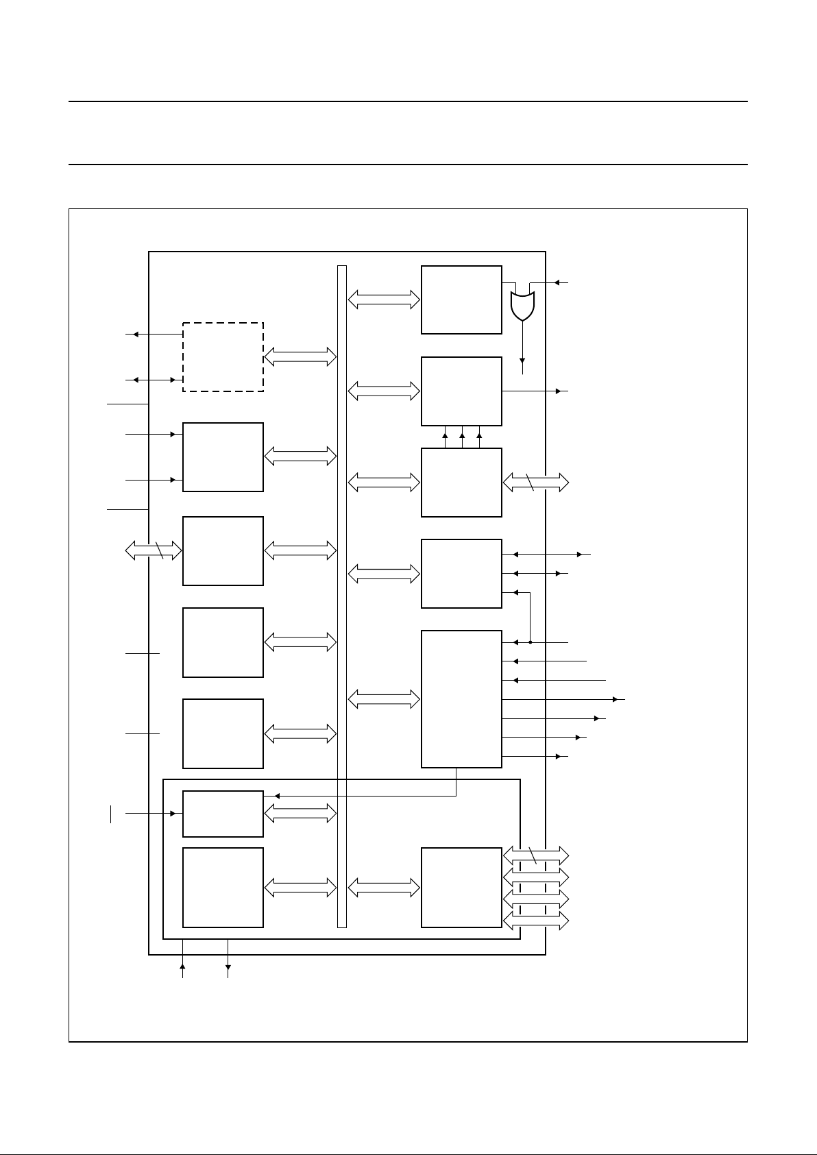
4 BLOCK DIAGRAM
full pagewidth
MGG021
4
10
4
XTAL2
XTAL1
P3P2P1P0
PARALLEL
I/O PORTS
&
EXTERNAL BUS
14-BIT
PWM
WATCHDOG
TIMER
(T2)
TWO 16-BIT
TIMERS
(T0, T1)
80C51
core
excluding
ROM/RAM
CPU
PROGRAM
MEMORY
10 × 8-BIT
PWM
DDC
INTERFACE
MODE
DETECTION
INT0
DATA
MEMORY
4 × 8-BIT
DAC
4-BIT
ADC
SOFTWARE
I
2
C-BUS
SERIAL
I/O
8-bit
internal bus
internal reset
(4)
512 BYTES
RAM
P83C880
P83C180
P83C280
P83C380
P87C380
VSYNC
in
CLAMP
(3)
HSYNC
in
PATOUT
(3)
SCL1
(1)
PWM0 to PWM7
(2)
;
PWM8 to PWM9
(3)
PWM10
(1)
RESET
SDA1
(1)
HSYNC
out
(1)
CSYNC
in
(1)
VSYNC
out
(1)
V
DD
V
SS
V
SSA
V
DDA
INT1INT1 ADC0
(3)
DAC0 to DAC3
ADC1
(3)
SDA
(1)
SCL
(1)
Fig.1 Block diagram.
(1) Alternative function of Port 1.
(2) Alternative function of Port 2.
(3) Alternative function of Port 3.
(4) ROM: 8 kbytes (P83C880); 16 kbytes (P83C180); 24 kbytes (P83C280); 32 kbytes (P83C380). EPROM: 16 kbytes only in the P87C180A.

1997 Dec 12 6
Philips Semiconductors Product specification
Microcontrollers for monitors with DDC
interface, auto-sync detection and sync proc.
P83Cx80; P87C380
5 PINNING INFORMATION
5.1 Pinning
Fig.2 Pinning configuration for SDIP42.
handbook, halfpage
MGG020
1
2
42
41
3
4
5
6
7
8
9
10
11
12
13
14
15
16
17
18
19
20
40
39
38
37
36
35
34
33
32
31
30
29
28
27
26
25
24
23
2221
PWM8/CLAMP/P3.0
PWM9/PATOUT/P3.1
PWM10/P1.7
SCL/P1.0
SDA/P1.1
SCL1/P1.2
SDA1/P1.3
INT1/V
PP
ADC1/P3.3
ADC0/P3.2
V
DDA
V
SSA
DAC3
DAC2
DAC1
DAC0
RESET
P0.0
P0.1
P0.2
P0.3
PWM7/P2.7
PWM6/P2.6
PWM5/P2.5
PWM4/P2.4
PWM3/P2.3
PWM2/P2.2
PWM1/P2.1
PWM0/P2.0
XTAL1
XTAL2
V
DD
V
SS
HSYNCin/PROG
HSYNC
out
/P1.5
CSYNCin/P1.6
VSYNCin/OE
VSYNC
out
/P1.4
P0.7
P0.6
P0.5
P0.4
P83C880
P83C180
P83C280
P83C380
P87C380
1997 Dec 12 7
Philips Semiconductors Product specification
Microcontrollers for monitors with DDC
interface, auto-sync detection and sync proc.
P83Cx80; P87C380
5.2 Pin description
Table 2 Pin description for SDIP42 (SOT270-1)
SYMBOL PIN DESCRIPTION
PWM9/PATOUT/P3.1 41 PWM9 to PWM0: 8-bit Pulse Width Modulation outputs 9 to 0. Pin 41 and 42 can
also be used as the output pin of the test pattern display PATOUT and clamping out
signal CLAMP respectively; PATOUT and CLAMP always have the higher priority.
Alternative function general I/O ports; Port 3: P3.1 to P3.0 and
Port 2: P2.7 to P2.0.
PWM8/CLAMP/P3.0 42
PWM7/P2.7 1
PWM6/P2.6 2
PWM5/P2.5 3
PWM4/P2.4 4
PWM3/P2.3 5
PWM2/P2.2 6
PWM1/P2.1 7
PWM0/P2.0 8
XTAL1 9 Oscillator input pin for system clock.
XTAL2 10 Oscillator output pin for system clock.
V
DD
11 Digital power supply (+5 V).
V
SS
12 Digital ground.
HSYNC
in
/PROG 13 Horizontal sync input pin. During OTP programming it is used as the program pulse
input (PROG).
HSYNC
out
/P1.5 14 Horizontal sync output pin; alternative function: general I/O port P1.5.
CSYNC
in
/P1.6 15 Composite sync input pin; alternative function: general I/O port P1.6.
VSYNC
in
/OE 16 Vertical sync input pin. During OTP programming it is used as output strobe (OE).
VSYNC
out
/P1.4 17 Vertical sync output pin; alternative function: general I/O port P1.4.
P0.7 to P0.0 18 to 25 Port 0: general I/O ports; capability to drive LED.
RESET 26 Reset input; active HIGH initializes the device.
DAC0 to DAC3 27 to 30 8-bit DAC analog voltage output pins; output range: 0 to 5 V.
V
SSA
31 Analog ground for DAC and ADC.
V
DDA
32 Analog power supply (+5 V) for DAC and ADC.
ADC0/P3.2 33 ADC analog input pins; alternative function: general I/O ports P3.2 and P3.3.
ADC1/P3.3 34
INT1/V
PP
35 External interrupt input pin. During OTP programming it is used as programming
supply voltage pin; VPP= 12.75 V.
SDA1/P1.3 36 I
2
C-bus serial data I/O port for the DDC2 interface; alternative function: general I/O
port P1.3.
SCL1/P1.2 37 I
2
C-bus serial clock I/O port for the DDC2 interface; alternative function: general I/O
port P1.2.
SDA/P1.1 38 I
2
C-bus serial data I/O port; alternative function: general I/O port P1.1.
SCL/P1.0 39 I
2
C-bus serial clock I/O port; alternative function: general I/O port P1.0.
PWM10/P1.7 40 14-bit Pulse Width Modulation output 10; alternative function: general I/O port P1.7.

1997 Dec 12 8
Philips Semiconductors Product specification
Microcontrollers for monitors with DDC
interface, auto-sync detection and sync proc.
P83Cx80; P87C380
6 FUNCTIONAL DESCRIPTION
This chapter gives a brief overview of the device.
Detailed functional descriptions are given in the following
chapters:
Chapter 7 “Memory organization”
Chapter 8 “Interrupts”
Chapter 9 “Watchdog Timer”
Chapter 10 “Input/Output (I/O)”
Chapter 11 “Reduced power modes”
Chapter 12 “Oscillator”
Chapter 13 “Reset”
Chapter 14 “Analog control (DC)”
Chapter 15 “Analog-to-digital converter (ADC)”
Chapter 16 “Digital-to-analog converter (DAC)”
Chapter 17 “Display Data Channel (DDC) interface”
Chapter 18 “I2C-bus Interface”
Chapter 19 “Hardware mode detection”
Chapter 20 “Power management”
Chapter 21 “Control modes”.
6.1 General
The P83C880, P83C180, P83C280, P83C380 and
P87C380 8-bit microcontrollers are manufactured in an
advanced CMOS process and are derivatives of the
80C51 microcontroller family. They have the same
instruction set as the 80C51.
They contain 512 bytes of data memory (RAM). ROM:
8 kbytes (P83C880); 16 kbytes (P83C180); 24 kbytes
(P83C280); 32 kbytes (P83C380) and 16 kbytes of
EPROM for the P87C180. The microcontrollers are
intended for use in monitors ranging from 14" to 21" that
can be controlled from the outside (e.g. by a PC) via the
external DDC interface.
In addition to the 80C51 standard functions, they provide a
number of dedicated hardware functions for monitor
application. Eight general I/O ports plus 20 functions
combined I/O ports cater for application requirements
adequately.
Ten sets of 8-bit PWM deliver the digital waveform for
analog control purposes. One 14-bit PWM can support
F to V application. The keyboard interface is achieved via
a 4-bit ADC. A Watchdog Timer with a maximum count
period of 5 s prevents the processor running out of control
due to malfunction. Four channels of linear DAC with 8-bit
resolution support more accurate analog controls.
One software I
2
C-bus interface is dedicated for the internal
connection. A DDC interface will cover all DDC protocols,
including DDC1, DDC2B, DDC2AB and DDC2B+.
A hardware mode detector will facilitate mode detection
even in power reduced modes, e.g. Idle mode.
The versatile HSYNC and VSYNC outputs can be
generated to serve the desired application. In the free
running mode, two display patterns can highlight the status
of the monitor. Accordingly, the following items will be
supported by these microcontrollers:
• Mode detection for:
– Horizontal sync (HSYNC) frequencies from below
15 kHz up to 150 kHz
– Vertical sync (VSYNC) frequencies from below 40 Hz
up to 200 Hz
• ACCESS.bus interfacing with external devices, e.g. PCs
• DDC1, DDC2B, DDC2AB and DDC2B+ protocols as
defined in the VESA DDC standard
• Device Power Management Signalling (DPMS) as
described in VESA DPMS proposal.
Figure 1 shows the block diagram functions.

1997 Dec 12 9
Philips Semiconductors Product specification
Microcontrollers for monitors with DDC
interface, auto-sync detection and sync proc.
P83Cx80; P87C380
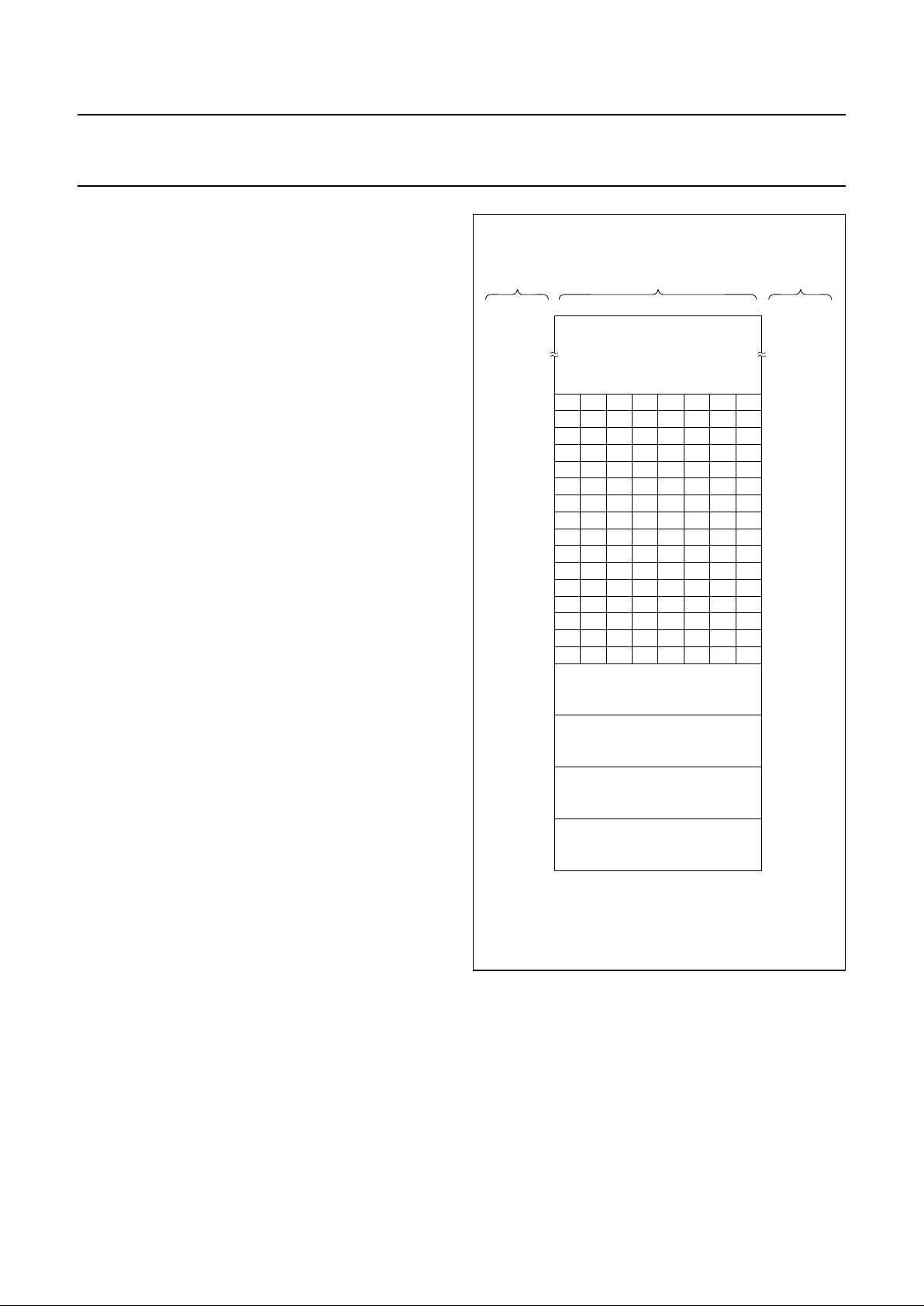
7 MEMORY ORGANIZATION
The Central Processing Unit (CPU) manipulates operands in two memory spaces. There are 512 bytes of internal data
memory, consisting of 256 bytes standard RAM and 256 bytes RAM buffer which is accessible as the Auxiliary RAM
(AUX-RAM) or addressed through DDCADR and RAMBUF. The memory map and address spaces are shown in Fig.3.
7.1 Program memory
The program memory consists of ROM: 8 kbytes (P83C880), 16 kbytes (P83C180), 24 kbytes (P83C280) and 32 kbytes
(P83C380). The program memory implemented in the P87C380 is a 16 kbytes EPROM (OTP).
7.2 Internal data memory
The internal data memory is divided into three physically separated parts: 256 bytes of RAM, 256 bytes of AUX-RAM,
and a 128 bytes Special Function Registers (SFRs) area. These can be addressed each in a different way as described
in Sections 7.2.1 to 7.2.3 and Table 3.
Table 3 Internal data memory map
Notes
1. RAM locations 0 to 127 can be addressed directly and indirectly as in the 80C51.
2. RAM locations 128 to 255 can only be addressed indirectly.
MEMORY LOCATION
ADDRESS MODE
POINTERS
DIRECT INDIRECT
RAM 0 to 127
(1)
X X address pointers are R0 and R1 of the selected register bank
128 to 255
(2)
− X
AUX-RAM 0 to 255 − X
(3)
address pointer DDCADR and RAMBUF
SFRs 128 to 255 X −−
ndbook, full pagewidth
MGG028
overlapped space
255
127
0
INTERNAL
program memory area
internal data memory area
32767
(1)
24575
(2)
16383
(3)
8191
(4)
0
INDIRECT
ONLY
INDIRECT
ONLY
DIRECT AND
INDIRECT
SPECIAL
FUNCTION
REGISTERS
AUX-RAM
BUFFER
255
0
Fig.3 Memory map and address spaces.
(1) P83C380 and P87C380.
(2) P83C280.
(3) P380C180.
(4) P83C880.
1997 Dec 12 10
Philips Semiconductors Product specification
Microcontrollers for monitors with DDC
interface, auto-sync detection and sync proc.
P83Cx80; P87C380
3. Indirect-addressable via MOVX-Datapointer or
MOVX-Ri instructions.
7.2.1 RAM
Four register banks, each 8 registers wide, occupy
locations 0 through 31 in the lower RAM area. Only one of
these banks may be enabled at a time. The next 16 bytes,
locations 32 through 47, contain 128 directly addressable
bit locations. The stack can be located anywhere in the
internal 256 bytes RAM. The stack depth is only limited by
the available internal RAM space of 256 bytes (see Fig.4).
7.2.2 S
PECIAL FUNCTION REGISTERS (SFRS)
The SFRs can only be addressed directly in the address
range from 128 to 255 (see Fig.3). Figure 5 gives an
overview of the Special Function Registers space. Sixteen
address in the SFRs space are both byte and
bit-addressable. The bit-addressable SFRs are those
whose address ends in 0H and FH. The bit addresses in
this area are 80H to FFH
7.2.3 AUX-RAM
AUX-RAM buffer 0 to 255 is indirectly addressable as
external data memory locations 0 to 255 via
MOVX-Datapointer instruction or via MOVX-Ri instruction.
Since the external access function is not available, any
access to AUX-RAM 0 to 255 will not affect the ports.
The 256 bytes of AUX-RAM buffer used to support DDC
interface is also available for system usage by indirect
addressing through the address pointer DDCADR and
data I/O buffer RAMBUF. The address pointer (DDCADR)
is equipped with the post increment capability to facilitate
the transfer of data in bulk (for details refer to Chapter 17).
However, it is also possible to address the AUX-RAM
buffer through MOVX command as usually used in the
internal RAM extension of 80C51 derivatives.
Fig.4 RAM bit addresses.
MBH079
7F 7E 7D 7C 7B 7A 79 78
77 76 75 74 73 72 71 70
6F 6E 6D 6C 6B 6A 69 68
67 66 65 64 63 62 61 60
5F 5E 5D 5C 5B 5A 59 58
57 56 55 54 53 52 51 50
4F 4E 4D 4C 4B 4A 49 48
47 46 45 44 43 42 41 40
3F 3E 3D 3C 3B 3A 39 38
37 36 35 34 33 32 31 30
2F 2E 2D 2C 2B 2A 29 28
27 26 25 24 23 22 21 20
1F 1E 1D 1C 1B 1A 19 18
17 16 15 14 13 12 11 10
0F 0E 0D 0C 0B 0A 09 08
07 06 05 04 03 02 01 00
18H
17H
10H
0FH
08H
07H
00H
24
23
31
16
15
8
7
0
BANK 0
BANK 1
BANK 2
BANK 3
32
33
34
35
36
37
38
39
40
41
42
43
44
45
46
47
(MSB) (LSB)
255
FFH
2FH
2EH
2DH
2CH
2BH
2AH
29H
28H
27H
26H
25H
24H
23H
22H
21H
20H
1FH
BYTE
ADDRESS
(DECIMAL)
BYTE
ADDRESS
(HEX)
BIT ADDRESS
(HEX)

1997 Dec 12 11
Philips Semiconductors Product specification
Microcontrollers for monitors with DDC
interface, auto-sync detection and sync proc.
P83Cx80; P87C380
handbook, full pagewidth
MGG029
FF
(MSB) (LSB)
255
MDCST
FFH
F8H
BYTE ADDRESS
(DECIMAL)
BYTE ADDRESS
(HEX)
BIT ADDRESS
(HEX)
FE FD FC FB FA F9 F8
F7
B
F0H F6 F5 F4 F3 F2 F1 F0
EF
PWME2
E8H EE ED EC EB EA E9 E8
C7
DFCON
C0H C6 C5 C4 C3 C2 C1 C0
BF
IP0
B8H BE BD BC BB BA B9 B8
B7
P3
B0H B6 B5 B4 B3 B2 B1 B0
AF
IEN0
A8H AE AD AC AB AA A9 A8
A7
P2
A0H A6 A5 A4 A3 A2 A1 A0
9F
not used
98H 9E 9D 9C 9B 9A 99 98
97
P1
90H 96 95 94 93 92 91 90
8F
TCON
88H 8E 8D 8C 8B 8A 89 88
87
P0
80H 86 85 84 83 82 81 80
E7
ACC
E0H E6 E5 E4 E3 E2 E1 E0
DF
S1CON
D8H
PSW
D0H
PWME1
C8H
DE DD DC DB DA D9 D8
D7 D6 D5 D4 D3 D2 D1 D0
CF CE CD CC CB CA C9 C8
Fig.5 Special Function Registers bit addresses.

1997 Dec 12 12
Philips Semiconductors Product specification
Microcontrollers for monitors with DDC
interface, auto-sync detection and sync proc.
P83Cx80; P87C380
7.3 Additional Special Function Registers
The standard SFRs as used in 80C51 and the SFRs for some typical derivative functions like I2C-bus interface, Timer,
etc. are described in the
“Data Handbook IC20”
. The specific SFRs for the P83C880 are introduced in the relevant
chapters. Some SFRs which are not mentioned or not dedicated to a certain function will be described in the following
sections.
All new additional SFRs used in the P83C880 are listed in Table 4. However, only some of them will be explained in detail
in Sections 7.3.1 to 7.3.7.
Table 4 Overview of additional SFRs
Notes
1. X = don’t care; even if it’s implemented.
2. B = both read/write and R
o
= read only; accessible for the entire byte or an individual bit. U = not implemented.
REGISTER DESCRIPTION ADDRESS RESET VALUE
(1)
READ/WRITE
(2)
RAMBUF RAM Buffer I/O Interface Register 9CH XXXXXXXX B
DDCCON DDC Control Register 9DH X00X0000 UBBUBBBB
DDCADR DDC Address Pointer 9EH 00000000 B
DDCDAT Data Shift Register for DDC1 9FH 00000000 B
DFCON Miscellaneous Control Register C0H 10000000 B
ADCDAT ADC Control Register C1H XX000000 UUBBBBBR
O
PWM10H PWM High-byte Data Latch C6H 00000000 B
PWM10L PWM Low-byte Data Latch C7H 10000000 B
S1CON Control Register for DDC2 D8H 00000000 B
S1STA Status Register for DDC2 D9H 11111000 R
o
S1DAT Data Shift Register for DDC2 DAH 00000000 B
S1ADR Address Register for DDC2 DBH 00000000 B
PWME1 PWM Output Control Register 1 C8H 00000000 B
PWME2 PWM Output Control Register 2 E8H 00000000 B
PWM0 to PWM9 Data Latches for 8-bit PWMs C9H to CFH,
EDH to EFH
00000000 B
DAC0 to DAC3 8-bit Data Latches for 8-bit DACs E9H to ECH 00000000 B
HFP Free run Control Register for HSYNC
out
F6H 01100000 B
HFPOPW Free run and Pulse width for HSYNC
out
F7H 00011111 B
MDCST Mode Detect Control and Status Register F8H 1X000000 BUBBRRRR
VFP Free run Control Register for VSYNC
out
F9H 01000000 B
VFPOPW Free run and Pulse width for VSYNC
out
FAH XX000101 B
PULCNT Pulse Generation Control Register FBH 00000000 B
HFHIGH Horizontal Period Counting High-byte
Register
FCH 00000000 R
o
VFHIGH Vertical Period Counting High-byte Register FDH 00000000 R
o
VFLHFL Vertical and Horizontal Period Counting
Low-nibbles Register
FEH 00000000 R
o
T2 Watchdog Timer Data Register FFH 00000000 B
1997 Dec 12 13
Philips Semiconductors Product specification
Microcontrollers for monitors with DDC
interface, auto-sync detection and sync proc.
P83Cx80; P87C380
7.3.1 RAM BUFFER I/O INTERFACE REGISTER (RAMBUF)
RAMBUF is used as an I/O interface to the RAM buffer. If it is associated with the address pointer DDCADR which is
equipped with the capability of post increment, then it will be convenient to transfer the consecutive data stream. This
feature is useful to support the DDC/EDID data transfer.
Table 5 RAM Buffer I/O Interface Register (SFR address 9CH)
Table 6 Description of RAMBUF bits
7.3.2 M
ISCELLANEOUS CONTROL REGISTER (DFCON)
This register is bit-addressable.
Table 7 Miscellaneous Control Register (SFR address C0H)
Table 8 Description of DFCON bits
76543210
RAMBUF.7 RAMBUF.6 RAMBUF.5 RAMBUF.4 RAMBUF.3 RAMBUF.2 RAMBUF.1 RAMBUF.0
BIT SYMBOL DESCRIPTION
7 to 0 RAMBUF.7 to RAMBUF.0 8-bit data which is read from or to be written into RAM buffer
76543210
EW2 SOGE SYNCE DDCE S1E ADCE P14LVL P8LVL
BIT SYMBOL DESCRIPTION
7 EW2 Watchdog Timer enable flag. This flag is associated with the flags, EW1 (SFR
PWM10H) and EW0 in (SFR PWM10L) to form the enable/disable control key for the
Watchdog Timer (see Chapter 9). The Watchdog Timer is only disabled by
EW2 to EW0 = 101, else it is kept enabled for the rest of the combinations.
6 SOGE CSYNC
in
enable for pin CSYNCin/P1.6. If SOGE = 1, the pin function is CSYNCin. If
SOGE = 0, the pin function is I/O port P1.6.
5 SYNCE Sync separated signals output enable for pins VSYNC
out
/P1.4 and HSYNC
out
/P1.5.
If SYNCE = 1, the pins function as VSYNC
out
and HSYNC
out
respectively.
If SYNCE = 0, the pins function as I/O ports P1.4 and P1.5 respectively.
4 DDCE Enable for DDC interface pins SCL1/P1.2 and SDA1/P1.3. If DDCE = 1, the pins
function as SCL1 and SDA1 respectively for the DDC interface. If DDCE = 0, the pins
function as I/O ports P1.2 and P1.3 respectively.
3 S1E Enable for I
2
C-bus interface pins SCL/P1.0 and SDA/P1.1. If S1E = 1, the pins
function as SCL and SDA respectively for the I2C-bus interface. If S1E = 0, the pins
function as I/O ports P1.0 and P1.1 respectively.
1997 Dec 12 14
Philips Semiconductors Product specification
Microcontrollers for monitors with DDC
interface, auto-sync detection and sync proc.
P83Cx80; P87C380
7.3.3 ADC CONTROL REGISTER (ADCDAT)
Table 9 ADC Control Register (SFR address C1H)
Table 10 Description of ADCDAT bits
7.3.4 14-
BIT PWM DATA LATCHES (PWM10H AND PWM10L)
Table 11 PWM High-byte Data Latch (PWM10H; SFR address C6H)
Table 12 Description of PWM10H bits
2 ADCE ADC channel enable. This flag enables the ADC function and also switches the pins
ADC0/P3.2 and ADC1/P3.3 to the ADC inputs function. If ADCE = 1, the ADC function
is enabled and the pin functions are ADC0 and ADC1 respectively. If ADCE = 0, the
ADC function is disabled and the pin functions are I/O ports P3.2 and P3.3 respectively.
1 P14LVL Polarity selection bit for the PWM10 output (14-bit PWM). If P14LVL = 1, PWM10
output is inverted. If P14LVL = 0, PWM10 output is not inverted.
0 P8LVL Polarity selection bit for the PWM0 to PMM9 outputs (8-bit PWM). If P8LVL = 1,
PWM0 to PWM9 outputs are inverted. If P8LVL= 0, PWM0 to PWM9 outputs are not
inverted.
76543210
−−DACHL DAC3 DAC2 DAC1 DAC0 COMP
BIT SYMBOL DESCRIPTION
7 to 6 − Reserved.
5 DACHL ADC input channels selection. If DACHL = 1, then input channel
ADC1 is selected. If DACHL = 0, then input channel ADC0 is selected.
4 to 1 DAC3 to DAC0 Reference voltage level selection. The 4 bits select the analog output
voltage (V
ref
) of the 8-bit DAC. For V
ref
values see Table 31.
0 COMP Comparison result; read only. If COMP = 1, then the ADC input
voltage is higher than the reference voltage. If COMP = 0, then the ADC
input voltage is lower than the reference voltage.
76543210
EW1 PWM10H.6 PWM10H.5 PWM10H.4 PWM10H.3 PWM10H.2 PWM10H.1 PWM10H.0
BIT SYMBOL DESCRIPTION
7 EW1 Watchdog Timer enable flag. This flag is associated with the flag EW2
(SFR DFCON) and EW0 (SFR PWM10L) to form the enable/disable
control key for the Watchdog Timer; see Tables 8 and 14.
6 to 0 PWM10H.6 to PWM10H.0 7 upper data bits for the 14-bit PWM.
BIT SYMBOL DESCRIPTION

1997 Dec 12 15
Philips Semiconductors Product specification
Microcontrollers for monitors with DDC
interface, auto-sync detection and sync proc.
P83Cx80; P87C380
Table 13 PWM Low-byte Data Latch (PWM10L; SFR address C7H)
Table 14 Description of PWM10L bits
7.3.5 PWM O
UTPUT CONTROL REGISTER 1 (PWME1)
Table 15 PWM Output Control Register 1 (SFR address C8H)
Table 16 Description of PWME1 bits
76543210
EW0 PWM10L.6 PWM10L.5 PWM10L.4 PWM10L.3 PWM10L.2 PWM10L.1 PWM10L.0
BIT SYMBOL DESCRIPTION
7 EW0 Watchdog Timer enable flag. This flag is associated with the flag EW2
(SFR DFCON) and EW1 (SFR PWM10H) to form the enable/disable
control key for the Watchdog Timer; see Table 8 and 12.
6 to 0 PWM10L.6to PWM10L.0 7 lower data bits for the 14-bit PWM.
76543210
PWME1.7 PWME1.6 PWME1.5 PWME1.4 PWME1.3 PWME1.2 PWME1.1 PWME1.0
BIT SYMBOL DESCRIPTION
7 to 0 PWME1.7
to
PWME1.0
PWM outputs enable; n=7to0. If PWME1.n = 1, the corresponding PWM is enabled
and pins PWMn/P2.n are switched to PWMn outputs. If PWME1.n = 0, the
corresponding PWM is disabled and pins PWMn/P2.n are switched to I/O ports P2.n
function.

1997 Dec 12 16
Philips Semiconductors Product specification
Microcontrollers for monitors with DDC
interface, auto-sync detection and sync proc.
P83Cx80; P87C380
7.3.6 PWM OUTPUT CONTROL REGISTER 2 (PWME2)
Table 17 PWM Output Control Register 2 (SFR address E8H)
Table 18 Description of PWME2 bits
7.3.7 D
ATA LATCHES FOR 8-BIT PWMS (PWM0 TO PWM9)
Table 19 Data Latches for 8-bit PWMs (n = 0 to 9; SFR address C9H to CFH and EDH to EFH)
Table 20 Description of PWM0 to PWM9 bits
76543210
PATENA DACE3 DACE2 DACE1 DACE0 PWME2.2 PWME2.1 PWME2.0
BIT SYMBOL DESCRIPTION
7 PATENA PATOUT (pattern output) enable. If PATENA = 1, the pin
PWM9/PATOUT/P3.1 is switched to the PATOUT (display test pattern)
output. If PATENA = 0, the PATOUT function is disabled. The PATOUT
function always overrides other alternative functions such as PWM9 and
P3.1.
6 to 3 DACE3 to DACE0 DAC outputs enable (n=3to0). If DACEn = 1, the corresponding
DACs: DAC3 to DAC0 are enabled. If DACEn = 0, the corresponding
DACs: DAC3 to DAC0 are disabled.
2 to 0 PWME2.2 to PWME2.0 PWM outputs enable; n = 2 to 0. If PWME2.n = 1, the corresponding
PWMs: PWM8, PWM9 and PWM10, are enabled by PWME2.2,
PWME2.1 and PWME2.0 respectively and pins PWM8/CLAMP/P3.0,
PWM9/PATOUT/P3.1 and PWM10/P1.7 are switched to PWM output. If
PWME2.n = 0, the corresponding PWM is disabled. Pins
PWM8/CLAMP/P3.0, PWM9/PATOUT/P3.1 and PWM10/P1.7 are
switched to I/O port functions P3.0, P3.1 and P1.7 respectively.
76543210
PWMn.7 PWMn.6 PWMn.5 PWMn.4 PWMn.3 PWMn.2 PWMn.1 PWMn.0
BIT SYMBOL DESCRIPTION
7 to 0 PWMn.7 to PWMn.0 8-bit data for PWM channel n (n = 0 to 9)

1997 Dec 12 17
Philips Semiconductors Product specification
Microcontrollers for monitors with DDC
interface, auto-sync detection and sync proc.
P83Cx80; P87C380
8 INTERRUPTS
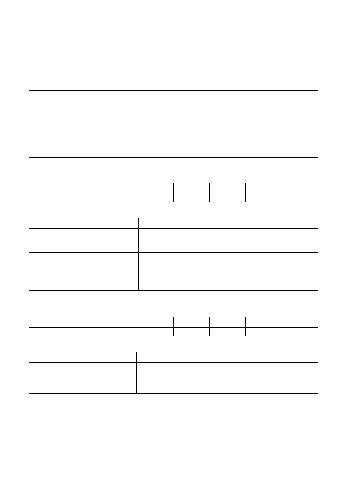
The P83C880 has 5 interrupt sources; these are shown in
Fig.6.
Interrupt INT1 is generated as in a normal 80C51 device.
By means of IT1 in SFR TCON this interrupt can be
selected to be:
• Level sensitive, when IT1 = LOW; INT1 must be inactive
before a return from interrupt instruction (RETI) is given,
otherwise the same interrupt will occur again.
• Edge sensitive, when IT1 = HIGH; the internal hardware
will reset the latch when the LCALL instruction is
executed for the vector address (see Table 21).
Interrupt
INT0 is generated by the mode change of mode
detector. Interrupt INT0 is selected as edge or level
sensitive by the state of the IT0 bit in the SFR TCON.
However, it is recommended to always set IT0 to HIGH
(edge sensitive) so that IE0 will be reset by the internal
hardware when the LCALL instruction is executed for the
vector address.
Timer 0 and Timer 1 interrupts are generated by TF0 and
TF1 which are set by an overflow of their respective
Timer/Counter registers (except for Timer 0 in Mode 3;
see
“Data Handbook IC20; 80C51 Family; Chapter
Timer/Counters”
). When a timer interrupt is generated, the
interrupt flag is cleared by the internal hardware when the
LCALL instruction is executed for the vector address.
The DDC interrupt is generated either by bit SI (SFR
S1CON) for DDC2B/DDC2AB/DDC2B+ protocols or by bit
DDC_int (SFR DDCCON) or by bit SWHINT (SFR
DDCCON). These flags must be cleared by software.
All bits that generate interrupts can be set or cleared by
software, with the same result as though it had been set or
cleared by hardware. That is, interrupts can be generated
or pending interrupts can be cancelled in software.
Each of these interrupts sources can be individually
enabled or disabled by setting or clearing the bit in Special
Function Register IE (see Table 23). IE also contains a
global disable bit EA, which disables all interrupts at once.
8.1 Priority level structure
The priority level of each interrupt source can be
individually programmed by setting or clearing a bit in
Special Function Register IP (see Table 25). A low priority
interrupt can itself be interrupted by a high priority
interrupt, but not by another low priority interrupt. A high
priority interrupt can not be interrupted by another interrupt
source.
If two requests of different priority levels are received
simultaneously, the request of higher priority level is
serviced. If request of the same priority level is received
simultaneously, an internal polling sequence determines
which request is serviced. Thus within each priority level
there is a second priority structure determined as shown in
Table 21. The IP register contains a number of reserved
(in 80C51) bits: IP.7, IP.6 and IP.4. User software should
not write logic 1s to these positions, since they may be
used in other 80C51 family products.
Table 21 Priority within levels
Note
1. The ‘Priority within level’ structure is only used to
resolve simultaneous requests of the same priority
level.
SOURCE PRIORITY WITHIN LEVEL
(1)
IE0′ 1 (highest)
SI 2
TF0 3
IE1′ 4
TF1 5 (lowest)
1997 Dec 12 18
Philips Semiconductors Product specification
Microcontrollers for monitors with DDC
interface, auto-sync detection and sync proc.
P83Cx80; P87C380
Fig.6 Interrupt sources.
handbook, full pagewidth
MGG024
TF0
TF0
'0'
'1'
interrupt
sources
Timer 0 overflow
Timer 1 overflow
TF1
CHREQ
TF1
S12
DDC INT
SWH INT
SI
IE1
IE1´
IT1
INT1
MUX
'0'
'1'
IE0
IE0´
IT0
INT0
MUX
external interrupt INT1
DDC2 (DDC2B/DDC2AB/DDC2B+) interrupt
DDC1 interrupt
SWITCH interrupt
mode change interrupt

1997 Dec 12 19
Philips Semiconductors Product specification
Microcontrollers for monitors with DDC
interface, auto-sync detection and sync proc.
P83Cx80; P87C380
8.2 How interrupts are handled
The interrupt flags are sampled at the S5P2 state of every
machine cycle. The samples are polled during the
following machine cycle. If one of the flags was in a set
condition at S5P2 of the preceding cycle, the polling cycle
will find it and the interrupt system will generate an LCALL
to the appropriate service routine, provided this hardware
generated LCALL is not blocked by any of the following
conditions:
1. An interrupt of equal priority or higher priority level is
already in progress.
2. The current (polling) cycle is not the final cycle in the
execution of the instruction in progress.
3. The instruction in progress is RETI or any write to the
IE or IP registers.
Any of these conditions will block the generation of the
LCALL to the interrupt service routine. Condition 2
ensures that the instruction in progress will be completed
before vectoring to any service routine.
Condition 3 ensures that if the instruction in progress is
RETI or any access to IE or IP, then at least one more
instruction will be executed before the interrupt is vectored
to.The polling cycle is repeated with each machine cycle,
and the values polled are the values that were present at
S5P2 of the previous machine cycle. Note that if an
interrupt flag is active but not being responded to for one
of the above mentioned conditions, and if the flag is still
inactive when the blocking condition is removed, then the
denied interrupt will not be serviced. In other words, the
fact that the interrupt flag was once active but not serviced
is not remembered. Every polling cycle is new.
The polling cycle/LCALL sequence is illustrated in
“Data
Handbook IC20; 80C51 family hardware description;
Figure: Interrupt Response Timing Diagram”
.
Note that if an interrupt of higher priority level becomes
active prior to S5P2 of the machine cycle labelled C3 (see
“Data Handbook IC20; 80C51 family hardware description;
Figure: Interrupt Response Timing Diagram”
), then in
accordance with the above rules it will be vectored to
during C5 and C6, without any instruction of the lower
priority routine having been executed. Thus the processor
acknowledges an interrupt request by executing a
hardware generated LCALL to the appropriate servicing
routine. The hardware generated LCALL pushes the
contents of the Program Counter on to the stack (but it
does not save the PSW) and reloads the PC with an
address that depends on the source of the interrupt being
vectored to as shown in Table 22.
Execution proceeds from that location until the RETI
instruction is encountered. The RETI instruction informs
the processor that the interrupt routine is no longer in
progress, then pops the top two bytes from the stack and
reloads the Program Counter. Execution of the interrupted
program continues from where it left off.
Note that a simple RET instruction would also return
execution to the interrupted program, but it would have left
the interrupt control system thinking an interrupt was still in
progress, making future interrupts impossible.
Table 22 Vector addresses
SOURCE VECTOR ADDRESS
IE0′ 0003H
SI 002BH
TF0 000BH
IE1′ 0013H
TF1 001BH
1997 Dec 12 20
Philips Semiconductors Product specification
Microcontrollers for monitors with DDC
interface, auto-sync detection and sync proc.
P83Cx80; P87C380
8.3 Interrupt Enable Register (IE)
Table 23 Interrupt Enable Register (SFR address A8H)
Table 24 Description of IE bits
8.4 Interrupt Priority Register (IP)
Table 25 Interrupt Priority Register (address B8H)
Table 26 Description of IP bits
76543210
EA − ES1 − ET1 EX1 ET0 EX0
BIT SYMBOL FUNCTION
7EADisable all interrupts. If EA = 0, then no interrupt will be acknowledged. If EA = 1, then
each interrupt source is individually enabled or disabled by setting or clearing its enable
bit.
6 − Reserved.
5 ES1 Enable DDC interface interrupt. If ES1 = 1, then DDC interface interrupt is enabled.
If ES1 = 0, then DDC interface interrupt is disabled.
4 − Reserved.
3 ET1 Enable Timer 1 overflow interrupt. If ET1 = 1, then the Timer 1 interrupt is enabled.
If ET1 = 0, then the Timer 1 interrupt is disabled.
2 EX1 Enable external interrupt 1. If EX1 = 1 then the External 1 interrupt is enabled.
If EX1 = 0 then the External 1 interrupt is disabled.
1 ET0 Enable Timer 0 overflow interrupt. If ET0 = 1 then the Timer 0 interrupt is enabled.
If ET0 = 0 then the Timer 0 interrupt is disabled.
0 EX0 Enable mode change. If EX0 = 1 then the mode change interrupt is enabled.
If EX0 = 0 then the mode change interrupt is disabled.
76543210
−−PS1 − PT1 PX1 PT0 PX0
BIT SYMBOL DESCRIPTION
7to6 − Reserved.
5 PS1 DDC interface Interrupt priority level. When PS1 = 1, DDC interface Interrupt is
assigned a high priority level.
4 − Reserved.
3 PT1 Timer 1 overflow interrupt priority level. When PT1 = 1, Timer 1 Overflow Interrupt is
assigned a high priority level.
2 PX1 External interrupt 1 priority level. When PX1 = 1, External Interrupt 1 priority is
assigned a high priority level.
1 PT0 Timer 0 overflow interrupt priority level. When PT0 = 1, Timer 0 Overflow Interrupt is
assigned a high priority level.
0 PX0 Mode change interrupt priority level. When PX0 = 1, Mode change Interrupt is
assigned a high priority level.

1997 Dec 12 21
Philips Semiconductors Product specification
Microcontrollers for monitors with DDC
interface, auto-sync detection and sync proc.
P83Cx80; P87C380
9 WATCHDOG TIMER
In addition to the standard timers, a Watchdog Timer
consisting of an 10-bit prescaler and an 8-bit timer is also
incorporated. The timer is increased every 19.5 ms for an
oscillator frequency of 16 MHz; this is derived from the
oscillator frequency (f
clk
) by the formula:
When a timer overflow occurs, the microcontroller is reset.
To prevent a system reset, the timer must be reloaded
before an overflows occurs, by the application software.
If the processor suffers a hardware/software malfunction,
the software will fail to reload the timer. This failure will
produce a reset upon overflow thus preventing the
processor running out of control.
The Watchdog Timer can only be reloaded if the condition
flag WLE (PCON.4) has been previously set by software.
At the moment the counter is loaded the condition flag is
automatically cleared.
In the Idle mode the Watchdog Timer and reset circuitry
remain active.
The time interval between timer reloading and the
occurrence of a reset, depends on the reloaded value.
f
timer
f
clk
304 1024×
-----------------------------
=
The Watchdog Timer’s time interval is:
Where T2 = decimal value of the T2 register contents and
t
1
= 15.2 µs (f
clk
= 10 MHz); t1= 12.7 µs (f
clk
= 12 MHz)
and t1=19µs (f
clk
= 16 MHz).
For example, this may range from 19.5 ms to 5.0 s when
using an oscillator frequency of 16 MHz.
Table 27 lists the resolution and the maximum time interval
of the Watchdog Timer using different system clocks.
The Watchdog Timer is controlled by the Watchdog control
bits:
• EW2; DFCON.7 (SFR address C0H)
• EW1; PWM10H.7 (SFR address C6H)
• EW0; PWM10L.7 (SFR address C6H).
Only when EW2 to EW0 = 101 the Watchdog Timer is
disabled and allows the Power-down mode to be enabled.
The rest of pattern combinations will keep the Watchdog
Timer enabled and disable the Power-down mode.
This security key with multiple flags split in two SFRs will
prevent the Watchdog Timer from being terminated
abnormally when the function of the Watchdog Timer is
needed.
tt
1
1024
256 T2–()
-----------------------------
×=
Table 27 Resolution and the maximum time interval of the WDT
f
clk
(MHz)
PRESCALER FACTOR
RESOLUTION
(ms)
MAXIMUM TIME INTERVAL
(s)
10 152 15.56 4.0
12 12.97 3.3
16 304 19.46 5.0

1997 Dec 12 22
Philips Semiconductors Product specification
Microcontrollers for monitors with DDC
interface, auto-sync detection and sync proc.
P83Cx80; P87C380
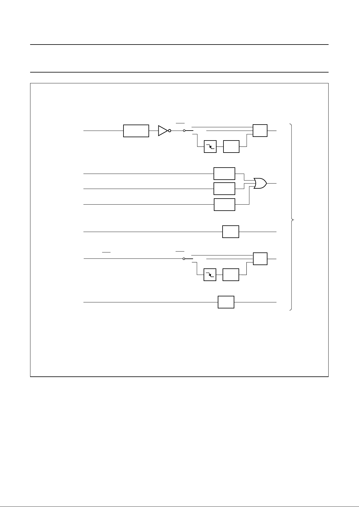
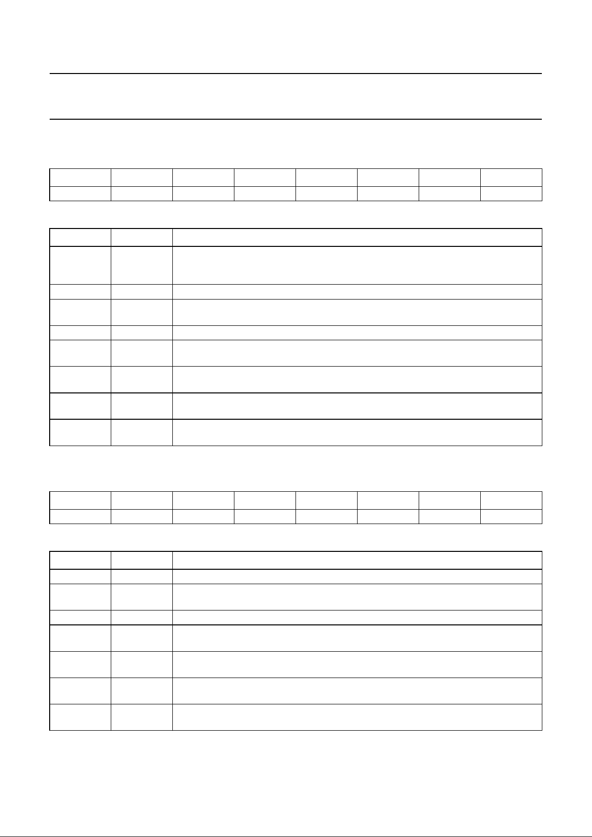
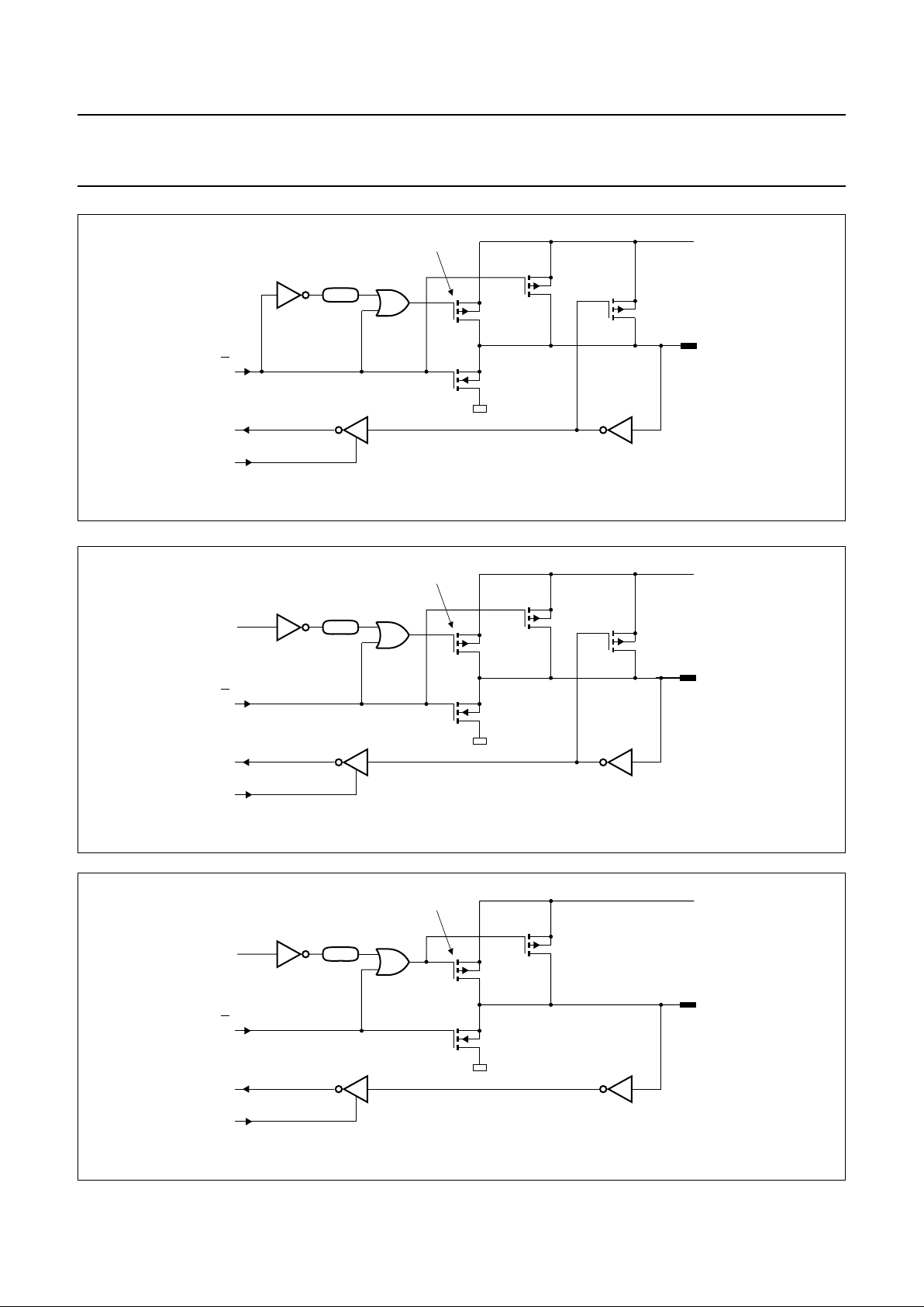
10 INPUT/OUTPUT (I/O)
The P83C880 has three 8-bit ports. Ports 0 to 2 are the
same as in the 80C51, with the exception of the additional
functions of Port 1 and Port 2. Port 3 only contains 4 bits.
Port 3 also has alternative functions.
All ports are bidirectional. Pins of which the alternative
function is not used may be used as normal bidirectional
I/Os.
The use of Port 1, Port 2 and Port 3 pins as an alternative
function is carried out automatically by the P83C880
provided the associated Special Function Register bit is
set HIGH.
The quasi-bidirectional type of port is applied for Port 1,
Port 2 and Port 3. Port 0 is an open-drain I/O port with the
capability to drive LED. However, for any port with an
alternative function, while the alternative function is
performed, the port type will be switched to the appropriate
type against a specific function. The port types:
quasi-bidirectional, pull-up and open-drain are shown in
Figs 7, 8 and 9 respectively.
10.1 The alternative functions for Port 0, Port 1,
Port 2 and Port 3
Port 0 Provides the low-order address in
programming/verify mode for the P87C380.
Port 1 Used for a number of special functions:
• 2 I/O pins for I
2
C-bus interface: SCL/P1.0 and
SDA/P1.1. The port type in this situation is set as
open-drain.
• 2 I/O pins for DDC interface: SCL1/P1.2 and
SDA1/P1.3. The port type in this situation is set
as open-drain.
• 2 I/O pins for the outputs of sync separation:
VSYNC
out
/P1.4 and HSYNC
out
/P1.5. The port
type in this situation is set as push-pull.
• One pin for the composite sync input of sync on
green mode: CSYNCin/P1.6. There is no pull-up
protection diode for this input pin.
• One pin for the 14-bit PWM output:
PWM10/P1.7. As PWM function, the port type is
open-drain.
Port 2 Two alternative functions are provided:
• High-order address in Programming/Verify mode
for P87C380.
• 8 channels of PWM outputs:
PWM0/P2.0 to P2.7/PWM7. The port type in this
situation is set as open-drain.
Port 3 Two alternative functions are provided:
• Two channels of PWM output:
PWM8/CLAMP/P3.0 and PWM9/PATOUT/P3.1.
The port type in this situation is set as
open-drain. PATOUT and CLAMP functions
always override PWM or port function even if
they are enabled. For the PATOUT (pattern
output) and CLAMP (clamping output)
application, the port type is defined as push-pull.
• Two pins for the software ADC input: ADC0/P3.2
and ADC1/P3.3. They are analog inputs.
10.2 EMI (Electromagnetic Interference) reduction
In order to reduce EMI (Electromagnetic Interference) the
following design measures have been taken:
• Slope control is implemented on all the I/O lines with
alternative functions of the PWM, I2C-bus and DDC
interface. For port pins P1.4 and P1.5, since the
alternative functions VSYNC
out
and HSYNC
out
are
incorporated, the driving capability is made as small as
possible to reduce radiation and the slope control
function is disabled to have a sharp output. Rise and fall
time (10% to 90%) for slope control are:
t
rf(min)
< rise/fall time < t
rf(max)
.
Refer to Chapter 27 for the detailed figures.
• Placing the VDD and VSS pins next to each other
• Double bonding of the VDD and VSS pins,
i.e. 2 bondpads for each pin
• Limiting the drive capability of clock drivers and
prechargers
• Applying slew rate controlled output drivers
• Internal decoupling of the supply of the CPU core.
1997 Dec 12 23
Philips Semiconductors Product specification
Microcontrollers for monitors with DDC
interface, auto-sync detection and sync proc.
P83Cx80; P87C380
Fig.7 Standard output with quasi-bidirectional port.
handbook, full pagewidth
MGG025
p1
p2
p3
input data
read port pin
2 oscillator
periods
n
strong pull-up
I/O PIN
V
DD
I1
Q
from port latch
INPUT
BUFFER
Fig.8 Standard output with the pull-up current source.
handbook, full pagewidth
MGG026
p1
p2
p3
input data
read port pin
2 oscillator
periods
n
'1'
strong pull-up
I/O PIN
V
DD
I1
Q
from port latch
INPUT
BUFFER
Fig.9 Standard output with the open-drain port.
handbook, full pagewidth
MGG027
p1
p2
input data
read port pin
2 oscillator
periods
n
'0'
strong pull-up
I/O PIN
V
DD
I1
Q
from port latch
INPUT
BUFFER

1997 Dec 12 24
Philips Semiconductors Product specification
Microcontrollers for monitors with DDC
interface, auto-sync detection and sync proc.
P83Cx80; P87C380
11 REDUCED POWER MODES
Two software selectable modes of reduced power
consumption are implemented. These are the Idle mode
and the Power-down mode.
11.1 Power Control Register (PCON)
The Idle mode and Power-down mode are activated by
software via the Power Control Register (SFR PCON).
Its hardware address is 87H. PCON is not bit addressable.
The reset value of PCON is 00H.
11.2 Idle mode
Idle mode operation permits the interrupts, I
2
C-bus
interface, DDC interface, mode detection and timer blocks
T0, T1 and T2 (Watchdog Timer) to function while the CPU
is halted. The following functions are switched off when the
microcontroller enters the Idle mode:
• CPU (halted)
• PWM0 to PWM10 (reset, output = HIGH)
• 4-bit ADC (aborted if conversion is in progress)
• DAC0 to DAC3 (output = indeterminate or frozen at the
final value prior to the Idle instruction; decided by
software).
The following functions remain active during Idle mode;
these functions may generate an interrupt or reset and
thus terminate the Idle mode:
• Timer 0, Timer 1 and Timer 2 (Watchdog Timer)
• The DDC interface
• External interrupt
• Mode detection.
The instruction that sets PCON.0 is the last instruction
executed in the normal operating mode before Idle mode
is activated. Once in the Idle mode, the CPU status is
preserved in its entirety: the Stack Pointer, Program
Counter, Program Status Word, Accumulator, RAM and all
other registers maintain their data during Idle mode.
The status of external pins during Idle mode is shown in
Table 28.
There are three ways to terminate the Idle mode:
• Activation of any enabled interrupt X0, T0, X1, T1 or S1
will cause PCON.0 to be cleared by hardware
terminating Idle mode. The interrupt is serviced, and
following return from interrupt instruction RETI, the next
instruction to be executed will be the one which follows
the instruction that wrote a logic 1 to PCON.0.
The flag bits GF0 and GF1 may be used to determine
whether the interrupt was received during normal
execution or during Idle mode. For example, the
instruction that writes to PCON.0 can also set or clear
both flag bits. When Idle mode is terminated by an
interrupt, the service routine can examine the status of
the flag bits.
• The second way of terminating the idle mode is with an
external hardware reset. Since the oscillator is still
running, the hardware reset is required to be active for
two machine cycles (24 oscillator periods) to complete
the reset operation.
• The third way of terminating the Idle mode is by an
internal watchdog reset.
In all cases the microcontroller restarts after 3 machine
cycles.
11.3 Power-down mode
In Power-down mode the system clock is halted. The
oscillator is frozen after setting the bit PD in the PCON
register.
The instruction that sets PCON.1 is the last executed prior
to going into the Power-down mode. Once in Power-down
mode, the oscillator is stopped.The content of the on-chip
RAM and the Special Function Registers are preserved.
Note that Power-down mode can not be entered when the
Watchdog Timer has been enabled.
The Power-down mode can be terminated by an external
reset in the same way as in the 80C51 (but the SFRs are
cleared due to RESET) or in addition by the external
interrupt, INT1.
A termination with INT1 does not affect the internal data
memory and the Special Function Registers. This gives
the possibility to exit from Power-down without changing
the port output levels. To terminate the Power-down mode
with an external interrupt, INT1 must be switched to be
level-sensitive and must be enabled. The external interrupt
input signal INT1 must be kept LOW till the oscillator has
restarted and stabilized. The instruction following the one
that put the device into the Power-down mode will be the
first one which will be executed after the wake-up.

1997 Dec 12 25
Philips Semiconductors Product specification
Microcontrollers for monitors with DDC
interface, auto-sync detection and sync proc.
P83Cx80; P87C380
11.4 Status of external pins
• If the HSYNC
out
, VSYNC
out
, PATOUT or CLAMP output
is selected (for selection see description in Tables 8
and 18) in Idle or Power-down mode, since sync
separation is still alive in Idle mode, HSYNC
out
,
VSYNC
out
, PATOUT or CLAMP output will be operating
as normal. In Power-down mode: HSYNC
out
, VSYNC
out
,
PATOUT or CLAMP output are pulled HIGH.
• In Idle or Power-down mode, if bit DDCE (SFR DFCON)
is set, the function of P1.2 and P1.3 will be switched to
the DDC interface pins SCL1 and SDA1 respectively. In
Idle mode SCL1 and SDA1 can be active only if DDC1
or DDC2 is enabled; otherwise these pins are in the
high-impedance (High-Z) state.
• If bit PWME.n (SFR PWME1/PWME2) is set, the
function of P1.7, P2.n, P3.0 and P3.1 will be switched to
the PWM output function. However, in both Idle and
Power-down modes, the output of those PWM pins are
pulled HIGH.
Table 28 Status of external pins during Idle and Power-down modes
MODE MEMORY
PORT0
TO
PORT 3
HSYNC;
VSYNC;
CLAMP;
PATOUT
SCL
AND
SDA
SCL1
AND
SDA1
PWM0
TO
PWM10
DAC0
TO
DAC3
Idle internal data operative High-Z operative HIGH unknown
Power-down internal data HIGH High-Z High-Z HIGH unknown

1997 Dec 12 26
Philips Semiconductors Product specification
Microcontrollers for monitors with DDC
interface, auto-sync detection and sync proc.
P83Cx80; P87C380
12 OSCILLATOR
The oscillator circuit of the P83C880 is a single-stage
inverting amplifier in a Pierce oscillator configuration. The
circuitry between XTAL1 and XTAL2 is basically an
inverter biased to the transfer point. Either a crystal or
ceramic resonator can be used as the feedback element to
complete the oscillator circuit. Both are operated in parallel
resonance.
XTAL1 is the high gain amplifier input, and XTAL2 is the
output (see Fig.10a). To drive the P83C880 externally,
XTAL1 is driven from an external source and XTAL2 left
open-circuit (see Fig.10b).
b. External clock drive.
handbook, halfpage
MBE312
XTAL1 XTAL2
n.c.
external clock
(not TTL compatible)
Fig.10 Oscillator configurations.
a. Crystal oscillator; C = 20 pF.
c. External clock drive for P87C380.
handbook, halfpage
XTAL1 XTAL2
external clock
(not TTL compatible)
MLC930 - 1
handbook, halfpage
MBE311
XTAL1 XTAL2
 Loading...