

DATA SH EET
Preliminary specification
Supersedes data of 1995 Oct 11
File under Integrated Circuits, IC18
1996 Jun 19
INTEGRATED CIRCUITS
P82C150
CAN Serial Linked I/O device
(SLIO) with digital and analog port
functions

Philips Semiconductors Preliminary specification
CAN Serial Linked I/O device (SLIO) with
digital and analog port functions
P82C150
1996 Jun 19 2
CONTENTS
1 FEATURES
2 GENERAL DESCRIPTION
3 ORDERING INFORMATION
4 BLOCK DIAGRAM
5 FUNCTIONAL DIAGRAM
6 PINNING INFORMATION
6.1 Pinning
6.2 Pin description
7 FUNCTIONAL DESCRIPTION
7.1 I/O functions
7.2 I/O registers
7.3 CAN functions
7.4 Initialization
7.5 P82C150 operation after RESET or change of
bus mode
8 LIMITING VALUES
9 DC CHARACTERISTICS
10 AC CHARACTERISTICS
11 APPLICATION INFORMATION
11.1 Maximum bus length
11.2 Start up sequence
11.3 External oscillator mode
11.4 Using digital I/O port functions
11.5 Using DPM
11.6 Using ADC
11.7 Using analog input port functions
11.8 CAN-bus system applications
12 PACKAGE OUTLINE
13 SOLDERING
13.1 Introduction
13.2 Reflow soldering
13.3 Wave soldering
13.4 Repairing soldered joints
14 DEFINITIONS
15 LIFE SUPPORT APPLICATIONS

1996 Jun 19 3
Philips Semiconductors Preliminary specification
CAN Serial Linked I/O device (SLIO) with
digital and analog port functions
P82C150
1 FEATURES
• Single-chip I/O device with CAN protocol controller
• Meets CAN protocol specification version 2.0 A and B
(passive) with restricted bit timing
• Fully integrated clock oscillator (no crystal required)
• 16 configurable digital or analog I/O port pins
• Each of the port pins individually configurable via
CAN-bus: port direction, port mode and event capture
facilities for inputs (event driven or polling)
• Up to sixteen digital inputs; automatic transmission of a
CAN message on a change on inputs individually
selectable
• Up to sixteen 3-state outputs
• Up to two quasi-analog outputs with 10-bit accuracy
• 10-bit analog-to-digital converter with up to six
multiplexed analog input channels (for accuracy see
Section 11.6)
• Two general purpose comparators
• Bit rate from 20 kbit/s up to 125 kbit/s using internal
oscillator
• Automatic bit rate detection and calibration
• Up to sixteen P82C150 nodes for one CAN-bus system
• Four identifier bits programmable
• SLIO functions controlled by a single intelligent node
(‘host’)
• Sleep-mode with wake-up via CAN-bus
• Differential CAN-bus input comparator and CAN-bus
output driver
• Supply voltage: 5 V ±4%
• Operating temperature: two ranges −40 to +85 °C and
−40 to +125 °C.
2 GENERAL DESCRIPTION
The P82C150 is a single-chip 16-bit I/O device including a
Controller Area Network (CAN) protocol controller with
automatic bit rate detection and calibration. It features 16
configurable I/O port pins with programmable direction,
digital and analog modes.
The P82C150 provides a configurable event capture
facility supporting automatic transmission caused by a
change on the port input pins.
The clock oscillator requires no external components,
thus, the cost of the CAN link is reduced significantly.
The P82C150 is a very cost-effective way to increase the
I/O capability of a microcontroller based CAN node as well
as to reduce the amount and complexity of wiring.
Advanced safety is provided by the CAN protocol.
Applications:
• Body electronics and instrumentation in automotive
applications
• Sensor/actuator interface in automotive and general
industrial applications
• Extension of I/O capabilities of microcontroller based
CAN nodes.
3 ORDERING INFORMATION
TYPE NUMBER
PACKAGE
TEMPERATURE
RANGE (°C)
NAME DESCRIPTION VERSION
P82C150 AFT
SO28 plastic small outline package; 28 leads; body width 7.5 mm SOT136-1
−40 to +85
P82C150 AHT −40 to +125
1996 Jun 19 4
Philips Semiconductors Preliminary specification
CAN Serial Linked I/O device (SLIO) with
digital and analog port functions
P82C150
4 BLOCK DIAGRAM
Fig.1 Block diagram.
handbook, full pagewidth
P82C150
ERROR
MANAGEMENT
LOGIC
RXO
21
RX1
22
19
18
BIT STREAM
PROCESSOR
input
comparator
TRANSMIT/
RECEIVE
LOGIC
PORT
LOGIC
IDENTIFIER
LATCH
23
4
20
OSCILLATOR
AND
CALIBRATOR
clock
8
REF
AV
DD
V
DD
+5 V
+5 V
9 to 16
5, 6, 7
1, 2, 3
P8 to P15
P5 to P7
P2 to P4
P0/CLK, P1
AV
SS
MHA064
CAN-bus
CAN-bus
17
P16
XMOD
25
26TX1
TX0
RST
16 I/O
port pins
1
/2 AV
DD
+
REFERENCE
VOLTAGE
27, 28
bus mode
bus mode
I/O
REGISTERS
24
V
SS
1996 Jun 19 5
Philips Semiconductors Preliminary specification
CAN Serial Linked I/O device (SLIO) with
digital and analog port functions
P82C150
5 FUNCTIONAL DIAGRAM
Fig.2 Functional diagram.
handbook, full pagewidth
P82C150
REF
RX0
RX1
TX0
P15
P13
P14
P12
P11
P10
P9
P8
P7
P6
P5
P4
P3
P2
P1
P0/CLK
RST (reset)
XMOD
CAN-bus inputs
analog-to-digital
comparator input
comparator
inputs
16-bit
digital I/O
MHA066
TX1
P16
CAN-bus outputs
ADC feedback output
multiplexed analog-
to-digital signal
analog
input
DPM1
output
analog inputs,
analog switches
DPM2
output
identifier
programming
reference
voltage output
VSS
AVSS
VDD
AVDD
1996 Jun 19 6
Philips Semiconductors Preliminary specification
CAN Serial Linked I/O device (SLIO) with
digital and analog port functions
P82C150
6 PINNING INFORMATION
6.1 Pinning
Fig.3 Pin configuration.
handbook, halfpage
26
27
24
23
22
21
20
19
18
17
16
15
1
2
3
4
5
6
7
8
9
10
11
12
13
P82C150
14
28
25
MHA065
P2
P3
P4
V
SS
XMOD
P6
P5
P7
V
DD
P8
P9
P10
P11
P12
P13
P1
P0/CLK
TX1
AV
SS
TX0
RST
RX1
RX0
AV
DD
REF
P16
P15
P14

1996 Jun 19 7
Philips Semiconductors Preliminary specification
CAN Serial Linked I/O device (SLIO) with
digital and analog port functions
P82C150
6.2 Pin description
Table 1 Pin description for P82C150; SO28; see note 1
Note
1. In this documentation the port pins are referred to by their symbols, not by their pin number. For example P15 means
I/O Port 15 at pin 16.
SYMBOL PIN DESCRIPTION
P2 1 I/O Ports P2 to P3; Identifier programming input.
P3 2
P4 3 I/O Port 4; DPM2 output.
V
SS
4 Ground, digital part (0 V; logic circuits and CAN-bus driver).
P5 5 I/O Ports P5 to P6; analog input.
P6 6
P7 7 I/O Port 7; analog input or analog-to-digital comparator 1 output.
V
DD
8 Power supply, digital part (+5 V; logic circuits and CAN-bus driver).
P8 9 I/O Port 8; analog input or comparator 3 output.
P9 10 I/O Port 9; analog input or comparator 2 output.
P10 11 I/O Port 10; comparator 3 inverting input or DPM1 output.
P11 12 I/O Port 11; comparator 3 non-inverting input.
P12 13 I/O Port 12; comparator 2 inverting input.
P13 14 I/O Port 13; comparator 2 non-inverting input.
P14 15 I/O Port 14; multiplexed analog signal.
P15 16 I/O Port 15; analog-to-digital comparator input.
P16 17 Feedback output of analog-to-digital converter.
AV
DD
18 Power supply, analog part (+5 V; CAN input, oscillator and reference).
REF 19 Reference voltage output (
1
⁄2× AVDD).
AV
SS
20 Ground, analog part (0 V; CAN input, oscillator, reference).
RX0 21 CAN-bus input.
RX1 22
RST 23 External reset input (active-HIGH) for internal oscillator mode; pulled to +5 V for external
oscillator mode (see Section 11.3).
XMOD 24 Connected to GND for internal oscillator mode; external reset input (active-LOW) for
external oscillator mode (see Section 11.3).
TX0 25 Open-drain CAN-bus output: dominant = LOW; recessive = floating.
TX1 26 Open-drain CAN-bus output: dominant = HIGH; recessive or at bus mode 2 floating.
P0/CLK 27 I/O Port P0, Identifier programming input in internal oscillator mode; clock input in external
oscillator mode (see Section 11.3).
P1 28 I/O Port P1; identifier programming input.
1996 Jun 19 8
Philips Semiconductors Preliminary specification
CAN Serial Linked I/O device (SLIO) with
digital and analog port functions
P82C150
7 FUNCTIONAL DESCRIPTION
7.1 I/O functions
The P82C150 provides 16 port pins (P15 to P0) which are
individually configurable via CAN-bus. Besides the digital
I/O functions some of these port pins provide analog I/O
functions.
7.1.1 D
IGITAL INPUT FUNCTIONS
Input levels HIGH and LOW on the port pins (P15 to P0)
can be read in two ways by the host node:
• Polling: a Remote Frame is sent to the P82C150 to be
answered by a Data Frame containing the Data Input
Register contents.
• Event capture: in case of edge-triggered mode, the
P82C150 sends the same Data Frame caused by the
event of a rising and/or falling edge on the
corresponding port pins (see Table 3).
7.1.2 D
IGITAL OUTPUT FUNCTIONS
The Data Output Register is set via a CAN message.
Its content is only output when the corresponding bits of
the Output Enable Register are set to logic 1s.
7.1.3 A
NALOG INPUT/OUTPUT FUNCTIONS
• Up to six multiplexed analog input signals for
analog-to-digital conversion or general purpose
• Up to two quasi-analog output channels (DPM;
Distributed Pulse Modulation)
• Two input comparators, for example for window
comparator applications
• A separate analog-to-digital input comparator with
feedback output.
Analog-to-digital converted digital results are obtained by
reading the Analog-to-Digital Conversion (ADC) Register.
Analog functions of each port pin are individually
controlled by the Analog Configuration Register.
Writing the I/O registers is done serially via CAN-bus by
Data Frames. The first data byte contains the register
address, and the second and third data bytes represent
the register contents. If a read only register is addressed,
the contents of the second and third data bytes are
ignored.
It is recommended to set unused port pins to HIGH
(100 kΩ resistor to V
DD
).
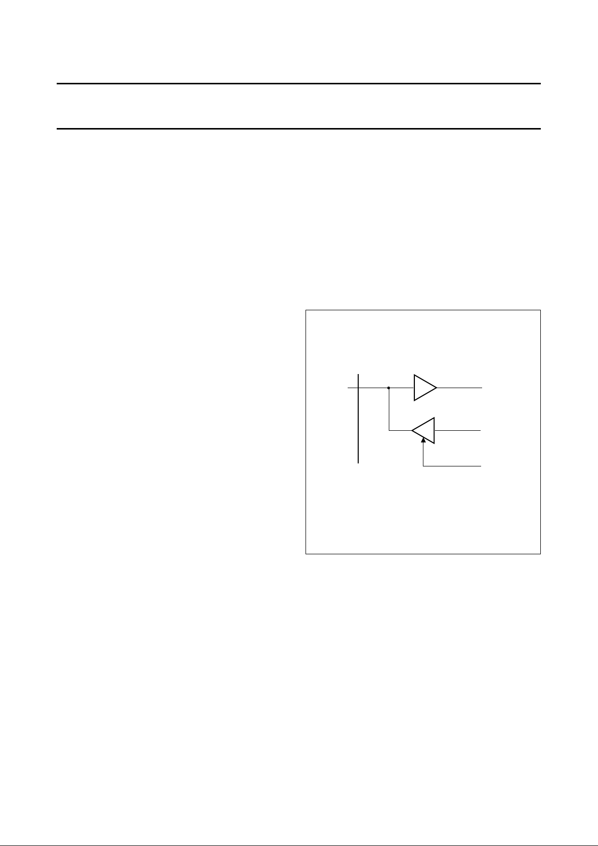
Fig.4 I/O port pins.
handbook, halfpage
Px
MHA068
DIx
DOx
OEx
3-state buffer
P82C150

1996 Jun 19 9
Philips Semiconductors Preliminary specification
CAN Serial Linked I/O device (SLIO) with
digital and analog port functions
P82C150
7.2 I/O registers
Table 2 I/O register map
15
(MSB)
1413121110987654321
0
(LSB)
ADDRESS 0: DATA INPUT
DI15 DI14 DI13 DI12 DI11 DI10 DI9 DI8 DI7 DI6 DI5 DI4 DI3 DI2 DI1 DI0
ADDRESS 1: POSITIVE EDGE
PE15 PE14 PE13 PE12 PE11 PE10 PE9 PE8 PE7 PE6 PE5 PE4 PE3 PE2 PE1 PE0
ADDRESS 2: NEGATIVE EDGE
NE15 NE14 NE13 NE12 NE11 NE10 NE9 NE8 NE7 NE6 NE5 NE4 NE3 NE2 NE1 NE0
ADDRESS 3: DATA OUTPUT
DO15 DO14 DO13 DO12 DO11 DO10 DO9 DO8 DO7 DO6 DO5 DO4 DO3 DO2 DO1 DO0
ADDRESS 4: OUTPUT ENABLE
OE15 OE14 OE13 OE12 OE11 OE10 OE9 OE8 OE7 OE6 OE5 OE4 OE3 OE2 OE1 OE0
ADDRESS 5: ANALOG CONFIGURATION
ADC OC3 OC2 OC1 0 M3 M2 M1 SW3 SW2 SW1 0 0 0 0 0
ADDRESS 6: DPM1
DP9DP8DP7DP6DP5DP4DP3DP2DP1DP0000000
A
DDRESS 7: DPM2
DQ9DQ8DQ7DQ6DQ5DQ4DQ3DQ2DQ1DQ0000000
A
DDRESS 8: ANALOG-TO-DIGITAL CONVERSION (ADC)
AD9 AD8 AD7 AD6 AD5 AD4 AD3 AD2 AD1 AD0 0 0 0 0 0 0

1996 Jun 19 10
Philips Semiconductors Preliminary specification
CAN Serial Linked I/O device (SLIO) with
digital and analog port functions
P82C150
7.2.1 DATA INPUT REGISTER (ADDRESS 0)
This read only register contains the states of port pins
P15 to P0 which are transmitted on request, or
automatically by change of one of the input levels,
provided that the respective input is configured to event
capture mode (see Table 3). When an edge is detected
the port state is loaded into the transmit buffer after the
Control Field of the triggered message is sent. Therefore a
delay for input settling is provided. If between edge
detection and transmission of the data input register
another input signal change at the input port occurs, the
corresponding data input register bit is overwritten by the
current input port value. Additionally the register content is
sent automatically after wake-up or bus mode change,
once the bit time has been calibrated (part of the ‘sign-on’
message).
7.2.2 P
OSITIVE EDGE REGISTER (ADDRESS 1)
This write only register contains configuration information
per port pin for the event capture facility.
The corresponding PE-bit (see Table 3) has to be set to
logic 1 to enable capturing of the rising edge.
7.2.3 N
EGATIVE EDGE REGISTER (ADDRESS 2)
This write only register contains configuration information
per port pin for the event capture facility.
The corresponding NE-bit (see Table 3) has to be set to
logic 1 to enable capturing of the falling edge.
The combination of PE and NE functions is possible.
7.2.4 D
ATA OUTPUT REGISTER (ADDRESS 3)
This write only register contains the output data for the port
pins. The output drivers are bitwise enabled by OE
(see Section 7.2.5). New data for the output port register
are processed and written to the output ports directly after
the corresponding CAN message to the P82C150 is
successfully checked and becomes valid.
7.2.5 O
UTPUT ENABLE REGISTER (ADDRESS 4)
This write only register controls the output drivers of the
port pins. The corresponding Output Enable Register bit
has to be set to logic 1 to enable an output driver. If set to
logic 0, the corresponding output driver is disabled
(floating; see Fig.7).
Table 3 Programming of the I/O registers to event capture on edge or to digital output
X = don’ t care; n=0to15.
FUNCTION
REGISTER CONTENTS OF PARTICULAR PORT PIN
POSITIVE EDGE
(BITS PEn)
NEGATIVE EDGE
(BITS NEn)
OUTPUT ENABLE
(BITS OEn)
Digital output X X 1
Digital input
Polling X X X
Event capture on edge
Rising 1 0 X
Falling 0 1 X
Rising and Falling 1 1 X

1996 Jun 19 11
Philips Semiconductors Preliminary specification
CAN Serial Linked I/O device (SLIO) with
digital and analog port functions
P82C150
7.2.6 ANALOG CONFIGURATION REGISTER (ADDRESS 5)
This read/write register contains the bits ADC, OC3 to
OC1, M3 to M1 and SW3 to SW1 (see Fig.7).
• ADC bit (analog-to-digital conversion start bit; write only
bit). The P82C150 starts an analog-to-digital conversion
cycle at ADC = 1 ended with the transmission of a
message containing the result. After that, the ADC bit is
reset automatically.
• OC3 to OC1 bits (comparator output data; read only
bits). The bits OC3 to OC1 represent the logical output
level of the analog comparators at input port pins P10,
P11, P12, P13 and P15. The P82C150 sends back the
logical output value of these comparators after having
received a Data Frame (see Section 7.3.3) addressing
the Analog Configuration Register. The comparator
outputs can be monitored at the output port pins P8, P9
and P7.
• M3 to M1 bits (multiplexer control bits; write only bits).
The logical value of the comparators is monitored on
port pins P8, P9 and P7 (see Fig.7) by setting M3 to M1
to logic 1, provided that these pins are configured as
outputs (OE = 1). Additionally the register content is
sent automatically when the corresponding port bits in
the Positive Edge Register and/or Negative Edge
Register and the corresponding bits in the Output
Enable Register are set.
• SW3 to SW1 (analog switch control bits; write only bits).
One of the analog switches S1 to S6 can be closed by
setting the switch bits to the corresponding value
(see Fig.7 and Table 4).
Table 4 Analog switch selection by SW3, SW2, SW1.
Note
1. Evidently if P14 is driven, it may not be connected to
any other driven pin via the internal analog switches
(avoid short-circuit!).
SW3 SW2 SW1 SWITCH STATE
0 0 0 no switch closed (S0); note 1
0 0 1 S1 closed
0 1 0 S2 closed
0 1 1 S3 closed
1 0 0 S4 closed
1 0 1 S5 closed
1 1 0 S6 closed
1 1 1 reserved
7.2.7 DPM1 REGISTER (ADDRESS 6)
This write only register contains data for a quasi-analog
output signal on port pin P10, which is generated by
Distributed Pulse Modulation (DPM; see Fig.9).
The Output Enable bit must be set for this functions
(OE10 = 1). The DPM1 output signal is inverted by setting
DO10 = 1. The number of output pulses during a DPM
period is given by the DPM1 Register value. These pulses
have 4 × t
CLK
length and are distributed over the DPM
period. An analog voltage is provided after smoothing the
output signal by an external RC combination.
7.2.8 DPM2 R
EGISTER (ADDRESS 7)
This write only register contains data for a quasi-analog
output signal on port pin P4. The function of the DPM2
corresponds to the definition of DPM1.
7.2.9 A
NALOG-TO-DIGITAL CONVERSION (ADC)
R
EGISTER (ADDRESS 8)
This read only register contains the result of the
analog-to-digital converted level of that I/O pin which was
selected by the SW bits. The conversion is started by
ADC-bit set to logic 1 (see Section 7.2.6), or by
transmitting a Data Frame addressing the ADC Register.
 Loading...