

Philips P32P4911A Datasheet

INTEGRATED CIRCUITS
DATA SH EET
P32P4911A
PRML Read Channel with PR4,
8/9 ENDEC, FWR Servo
Product Specification
1996 Jul 25

Philips Semiconductors Product specification
PRML Read Channel with PR4,
P32P4911A
8/9 ENDEC, FWR Servo
GENERAL DESCRIPTION
The Philips Semiconductors P32P4911A is a high performance BiCMOS read channel IC that provides all of the
functions needed to implement an entire Partial Response Class 4 (PR4) read channel for zoned recording hard disk
drive systems with data rates from 42 to 125 Mbit/s or 33 to 100 Mbit/s. Functional blocks include AGC, programmable
filter, adaptive transversal filter, Viterbi qualifier, 8,9 GCR ENDEC, data synchronizer, time base generator, and FWR
servo.
Programmable functions such as data rate, filter cutoff, filter boost, etc., are controlled by writing to the serial port
registers so no external component changes are required to change zones.
The part requires a single +5V power supply. The Philips Semiconductors P32P4911A utilizes an advanced BiCMOS
process technology along with advanced circuit design techniques which result in high performance devices with low
power consumption.
FEATURES
General:
• Register programmable data rates from 42 to 125 Mbit/s or 33 to 100 Mbit/s
• Sampled data read channel with Viterbi qualification
• Programmable filter for PR4 equalization
• Five tap transversal filter with adaptive PR4 equalization
• 8/9 GCR ENDEC
• Data Scrambler/Descrambler
• Presettable Precoder State
• Programmable write precompensation
• Low operating power (0.925 W typical at 5V)
• Register programmable power management (<5 mW power down mode)
• 4-bit nibble and byte-wide bi-directional NRZ data interfaces
• 8-bit Direct Write mode automatically configured for RCLK = VCO/8
• Serial interface port for access to internal program storage registers
• Single power supply (5V ± 10%)
• Small footprint, 100-lead LQFP package
1996 Jul 25 2 853-1850 17093
Philips Semiconductors Product specification
DSCLK
SSBYP
VIA+
VIA–
ON+
ON–
OD+
OD–
CPCNDP
DN
LEVEL OR
HYSTERESIS
PULSE
QUAL
PARALLEL
INTERFACE
BYP
HOLD
LOWZ
FASTREC
CONV
AGC
CHARGE
PUMP
MUX
TEST
POINY
MUX
DECISION
DIRECTED
PHASE
DETECTOR
CHARGE
PUMP
CODE WORD
BOUNDRY
DETECTOR
DAMPING
CONTROL
RCLK
SBD
NRZ0–7
NRZP
VCO SYNC
PATTERN
GEN
WRITE
PRECOMP
WD
WD
DWR
DWI
DWI
WCLK
MUX
MUX
SG
POWER
DOWN
CONTROL
SDEN
SCLK
SDATA
BYPS
PARALLEL
TO
SERIAL
MUX
DATA SYNCHRONIZER
RG
WG/WG
ATO
DSCLK
DSCLK
1/(N+1)
1/(M+1)
TIME BASE GENERATOR
RCLK
RCLK
SYNC
FIELD
COUNTER
To SFC
TBGOUT
CWBD
CWBD
WRITE
FLIP-FLOP
TBGOUT
CHANQUAL
CHANQUAL
TBGOUT
ASYMM FACTOR
LOW
ASYMM FACTOR
DACs
SG
SQUELCH
VMIN
SFC
DC
OFFSET
CANCEL
LOWZ
SFC
TPD
MUX
EN
AGCRST
UFDC
VCC
AGCDEL
WRDEL
LZTO
FDTO
HOLD
HOLD
LOWZ
SQUELCH
UFDC
SFC
MAXREF/2
SERVO
FASTREC
DUAL
“OR” TYPE
SYNC BYTE
DETECTOR
PARITY
GEN/CHK
FULLWAVE
RECTIFIER
VITERBI
DETECTOR
5–TAP
EQUALIZER
2-ADAPTIVE
2-PROG
AGC
CONTROL
LOGIC
SAMPLED
AGC
CHARGE
PUMP
PROGRAMMABLE
7TH-ORDER
LOW-PASS
FILTER
ASYMMETRIC 0’S
SERIAL
PORT
&
CONTROL
REGISTERS
AUTOMATIC
TRAINING & SYNC BYTE
GENERATOR
DESCRAMBLER
SCRAMBLER
PRECODER
9,8
((0,4/4)
DECODER
ATO
TEST
MUX
RCLK
CLOCK
GEN
AGC
AMP
DAC
FROM LEVEL
QUAL
VCO
VCO
CONTROL
LOGIC
2–BR
DAC
AGCREF
VRC
SREF
SDIEN
SEROUT
VPA
VPA
SG
0.2V
2.3V WRT
VPA
REFERENCE
SELVRC
3.2V
REFERENCE
NCLK
TPC
MUX
TPE
MUX
PARALLEL
TO
SERIAL
9,8
((0,4/4)
ENCODER
NIBBLE
INTERFACE
CHARGE
PUMP
PHASE/
FREQ
DETECTOR
PHASE/
FREQ
DETECTOR
VRDT
TPB–
TPB+
TPA–
TPA+
EQHOLD
PPOL
RDS/RDS
TPE
TPC–
TPC+
TPD–
TPD+
VRX
UFDC
FASTREC
LOWZ
SFWR
AGND3
AGND2
AGND1
DGND2
DGND1
PDWN
VPA3
VPA2
VPA1
VPD2
VPD1
FLTR2–
FLTR2+
FLTR1–
FLTR1+
RR
FREF
MAXREF
TPE
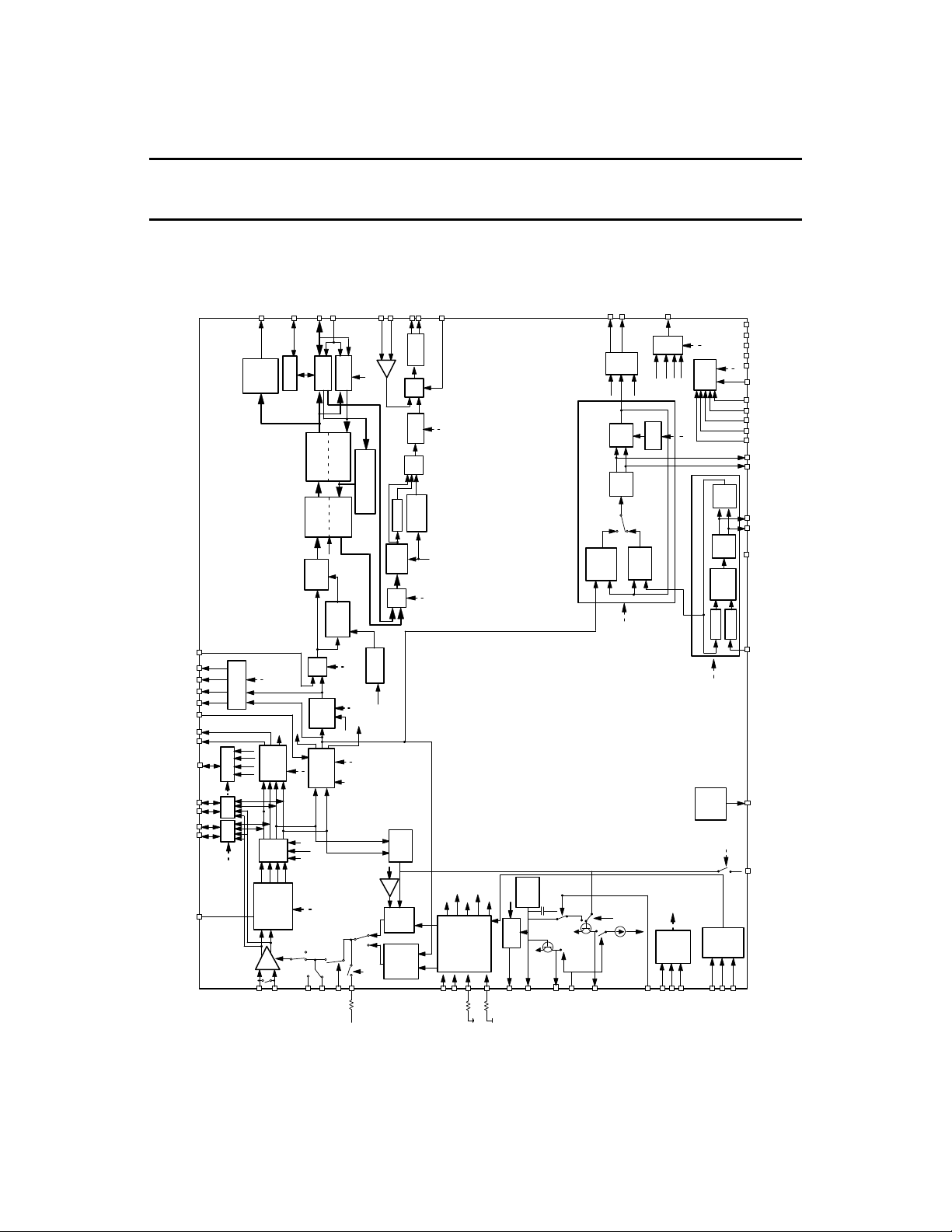
PRML Read Channel with PR4,
P32P4911A
8/9 ENDEC, FWR Servo
BLOCK DIAGRAM
SM00061
1996 Jul 25 3
Philips Semiconductors P32P4911A

Philips Semiconductors Product specification
PRML Read Channel with PR4,
P32P4911A
8/9 ENDEC, FWR Servo
Automatic Gain Control:
• Dual mode AGC, analog during acquisition, sampled during data reads
• Separate AGC level storage pins for data and servo
• Dual rate attack and decay charge pump for rapid AGC recovery (analog)
• Programmable, symmetric, charge pump currents for data reads (sampled)
• Charge pump currents track programmable data rate during data reads (sampled)
• Low drift AGC hold circuitry
• Low-Z circuitry at AGC input provides for rapid external coupling capacitor recovery
• AGC Amplifier squelch during Low-Z
• Wide bandwidth, precision full-wave rectifier
• Programmable AGC controls
– Separate external input pins for AGC hold, fast recovery, and Low-Z control
or
– Internal Low-Z and fast decay timing for rapid transient recovery and AGC acquisition. Timing set with external
resistors (2). Ultra fast decay current set with external resistor. AGC input impedance vs LOWZ = 5:1.
• 2-bit DAC to control AGC voltage in servo mode between 1.1 and 1.4 V
Filter/Equalizer:
• Programmable, 7-pole, continuous time filter provides:
– Channel filter and pulse slimming equalization for equalization to PR4
– Programmable cutoff frequency from 4 to 34 MHz
– Programmable boost /equalization of 0 to 13 dB
– Programmable "zeros" equalization provides time asymmetry compensation
– ±0.5 ns group delay variation from 0.3ƒc to ƒc, with ƒc = 34 MHz
– Minimizes size and power
– Low-Z switch at filter output for fast offset recovery
– No external coupling capacitors required
– DC offset compensation provided at filter output
– Five tap transversal filter for fine equalization to PR4
– Self adapting inner taps (symmetric)
– Programmable outer taps (symmetric, 4-bits)
– Equalization hold input
– "Zeros" channel quality output
– Amplitude asymmetry factor output
Pulse Qualification:
• Sampled Viterbi qualification of signal equalized to PR4
• Register programmable window or hysteresis pulse qualifier for servo reads
• Selectable RDS pulse width and polarity for servo gray code reads
1996 Jul 25 4

Philips Semiconductors Product specification
PRML Read Channel with PR4,
8/9 ENDEC, FWR Servo
Time Base Generator:
• Less than 1% frequency resolution
• Up to 141 MHz frequency output
• Independent M and N divide-by registers
• No active external components required
Data Separator:
• Fully integrated data separator includes data synchronizer and 8,9 GCR ENDEC
• Register programmable to 125 Mbit/s operation
• Fast Acquisition, sampled data phase lock loop
• Decision directed clock recovery from data samples
• Adaptive clock recovery thresholds
• Programmable damping ratio for data synchronizer PLL is constant for all data rates
• Data scrambler/descrambler to reduce fixed pattern effects
• 4-bit nibble and byte-wide NRZ data interfaces
• Nibble clock is available during byte-wide mode
• Time base tracking, programmable write precompensation
• Differential PECL write data output
• Integrated sync byte detection, single byte or dual ("or" type)
• Semi-auto training and sync byte generation available for single sync byte operation
• Surface defect scan mode
P32P4911A
Servo:
• Wide bandwidth, precision full-wave rectifier
• Separate, automatically selected, registers for servo ƒc, boost, and threshold
• SEROUT and SREF pins to provide a differential full-wave rectified servo signal
• SELVRC and SDIEN control pins for dc gain and offset calibration
• AGCREF output to provide 2-bit DAC-controlled voltage for applications requiring a fixed gain in servo mode
1996 Jul 25 5

Philips Semiconductors Product specification
PRML Read Channel with PR4,
P32P4911A
8/9 ENDEC, FWR Servo
FUNCTIONAL DESCRIPTION
The Philips Semiconductors P32P4911A implements a complete high performance PR4 read channel, including an
AGC, programmable filter/equalizer, adaptive transversal filter, Viterbi pulse qualifier, time base generator, data
separator with 8,9 ENDEC and scrambler/descrambler, and FWR servo, that supports data rates from 42 to 125 Mbit/s.
Data rates from 33 to 100 Mbit/s are supported by changing a single resistor.
A serial port is provided to write control data to the 17 internal program storage registers.
AGC Circuit Description
The automatic gain control (AGC) circuit is used to maintain a constant signal amplitude at the input of the pulse detector
and sampled data processor while the input to the amplifier varies. The circuit consists of an AGC loop that includes an
AGC amplifier, charge pump, programmable continuous time filter, and a precision, wide band, full wave rectifier.
Depending on whether the read is of servo or data type, the specific blocks utilized in the loop are slightly different. Both
loop paths are fully differential to minimize susceptibility to noise. AGC control can be programmably selected between
direct and timed modes.
AGC OPERATION IN SERVO READ MODE
During servo reads the loop consists of the AGC amplifier with a continuous dual rate charge pump, the programmable
continuous time filter, and the full wave rectifier. The gain of the AGC amplifier is controlled by the voltage stored on the
BYPS hold capacitor (C
at DP/DN (internal nodes) to the value programmed by the 2 SAGCLVL bits in the LDS register. These 2 bits allow
adjustment of the filter's normal output voltage from 1.10 to 1.40 Vppd. Attack currents lower the voltage at the BYPS
pin which reduces the amplifier gain. Decay currents raise the voltage at the BYPS pin which increases the amplifier
gain. The sensitivity of the amplifier gain to changes in the BYPS voltage is approximately 38 dB/V. When the voltage
at BYPS is equal to VRC, the gain from the AGC input to DP/DN will be about 24.9 dB. The charge pump is continuously
driven by the instantaneous voltage at DP/DN. When the signal at DP/DN is greater than 100% of the programmed AGC
level, the normal attack current (ICH) of 416.5 µA is used to reduce the amplifier gain. If the signal is greater than 125%
of the programmed level, the fast attack current (I
approach allows the AGC gain to be quickly decreased when it is too high and minimizes distortion when the proper AGC
level has been acquired. The 100% and 125% levels are relative to the selected AGC level in servo mode.
A constant normal decay current (ID) of 24.5 µA acts to increase the amplifier gain when the signal at DP/DN is less than
100% of the programmed AGC level. The large ratio (416.5 µA:24.5µA) of the normal attack and normal decay currents
enables the AGC loop to respond to the peak amplitudes of the incoming read signal rather than the average value. As
a result the AGC loop will not be able to quickly increase its gain if required to do so. A fast recovery mode is provided
to allow the gain to be rapidly increased to reduce recovery time between mode switches. In the fast recovery mode, the
decay current is increased by a factor of 8 to 196 µA (I
1.74 mA (I
It is recommended that the fast recovery mode be asserted when the AGC fields from a sector are being read. Typically,
this will be just after each transition of SG (Servo Gate), after powerup, and after WG/WG is de-asserted. For example,
if C
BYPS
0.5 µs * 196 µA/500 pF = 196 mV, which will allow the gain to increase by 6 dB in that time. If FASTREC is asserted for
0.5 µs in non-servo mode and C
1000 pF = 98 mV, which will allow the gain to increase by 3 dB in that time. It is recommended that LOWZ be asserted
for 0.5µs just prior to any assertion of FASTREC in order to null any internal DC offsets. However, it is possible to assert
both LOWZ and FASTREC simultaneously to reduce sector overhead. This method should be evaluated under the
actual system operating conditions.
The programmable AGC level in servo mode is provided to allow the servo demodulator dynamic range to be adjusted
over a narrow range.
). This has the effect of speeding up the AGC loop between 4 and 8 times.
CHFR
is 500 pF and FASTREC is asserted for 0.5 µs in servo mode, the voltage at BYPS can increase at most by
). The dual rate charge pump drives C
BYPS
) of 3.5 mA is used to reduce the gain very quickly. This dual rate
CHF
DFR
is 1000 pF, then the voltage at BYP can increase at most by 0.5 µs * 196 µA/
BYP
with currents that drive the differential voltage
BYPS
) and the attack current is increased by a factor of 4.18 to
1996 Jul 25 6

Philips Semiconductors Product specification
PRML Read Channel with PR4,
P32P4911A
8/9 ENDEC, FWR Servo
AGC OPERATION IN DATA READ MODE
For data reads, the loop described above is used until the data synchronizer is locked to the incoming VCO preamble,
except that the BYP hold capacitor (C
the normal attack current is 416.5 µA, and the fast attack current is 3.5 mA. The fast recovery mode decay current is
196 µA and the fast recovery mode attack current is 1.74 mA. The above mentioned attack and decay currents are not
scaled with the data rate setting. After the data synchronizer PLL is locked (SFC), the AGC loop is switched to include
the AGC amplifier with a sampled charge pump, the programmable continuous time filter, full wave rectifier, and the
sampling 5-tap equalizer to more accurately control the signal amplitude into the Viterbi qualifier. In this sampled AGC
mode, a symmetrical attack and decay charge pump is used. The "1" sample amplitudes are sampled and held and
compared to the ideal "1" value of 500 mV to generate the error current. The maximum charge pump current value can
be programmed from the Sample Loop Control Register to 0, 34, 68, or 102 µA for maximum data rate and will scale
downward with reduced Data Rate Register values.
AGC Control Modes
The AGC control mode is determined by the state of bit 6 (AGCSEL) of the Control Operating Register #1. If this bit is
0, then the direct, external AGC control method is selected, i.e., AGC uses external signals provided to the FASTREC,
LOWZ, and HOLD input pins. If bit 6 is a 1, the timed AGC control method is selected for generating the internal hold,
fast recovery, squelch, and Low-Z signals.
DIRECT AGC CONTROL MODE
For maximum application flexibility, all AGC mode control inputs are to be externally provided. When the LOWZ input is
High, Low-Z mode is activated. In the Low-Z mode, the AGC amplifier input resistance is reduced to allow quick recovery
of the AGC amplifier input AC coupling capacitors. The ratio of Low-Z to Non Low-Z resistance can be selected as either
15:1 or 5:1 by programming the LZTC bit in the Data Boost Register. During Low-Z mode, the time constant of the
internal AC coupling networks at the filter outputs are also reduced by the ratio determined by the LZTC bit. This time
constant is 300 ns in Low-Z and either 5 µs or 1.5 µs when not in Low-Z mode, depending on the state of the LZTC bit.
Low-Z also forces the AGC amplifier gain to be reduced to near 0 V/V. This mode should be activated during and for a
short time after a write operation. It should also be activated for a short time after each transition of the SG input and on
initial power up.
When theHOLD input is Low, the charge pumps are disabled. This de-activates the AGC loop. The AGC amplifier gain
will be held constant at a level set by the voltage at the BYP or BYPS pins. The value of the capacitor placed at these
pins should be selected to give adequate droop performance when in hold mode as well as to insure stability of the AGC
loop when it is active.
The signal provided to the FASTREC input pin determines if the AGC is in fast recovery mode. During the fast recovery
(FASTREC=1), the attack and decay currents are increased to allow faster recovery to the proper AGC level. If faster
recovery than is provided by FASTREC alone is desired, an ultra fast recovery can be effected by connecting a resistor
between the AGCRST pin and the positive supply VPA. If this resistor is present, whenever FASTREC is entered, the
voltage on the BYP or BYPS capacitor will be pulled up. This causes an extremely rapid increase in the AGC amplifier
gain. The ultra fast current will be disabled the first time that the signal at DP/DN reaches the 125% point. The FASTREC
attack and decay currents are used as long as the FASTREC pin is held High.
) is used instead of BYPS and (C
BYP
). The normal decay current is 24.5 µA,
BYPS
TIMED AGC CONTROL MODE
This timed AGC control mode differs from the direct control mode in that the external control inputs LOWZ, FASTREC,
and HOLD, are typically not used, and therefore, must be deasserted. The equivalent signals are generated internal to
the P32P4911A. These internal signals are generated by one-shots that are triggered by various conditions of the
WG/WG, SG, and PDWN inputs. The one-shot timings for the Low-Z and fastrec signals are set by the resistors
connected to the WRDEL and AGCDEL input pins, respectively and analog ground. The time Low-Z period = 0.1 µs *
(R
is set by the resistor connected between the AGCRST input pin and VPA. In the timed mode, the AGC shall use the
C
1996 Jul 25 7
+ 0.5) kΩ and the fast recovery period = 0.1 µs * (R
WRDEL
BYP
and C
for non-servo and servo modes respectively. The nominal and fast attack and decay currents are the
BYPS
+ 0.5) kΩ. The current for the ultra fast decay mode
AGCDEL
Philips Semiconductors Product specification
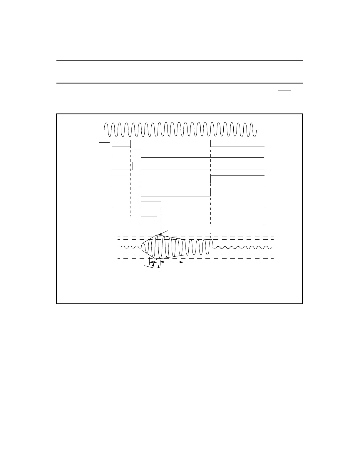
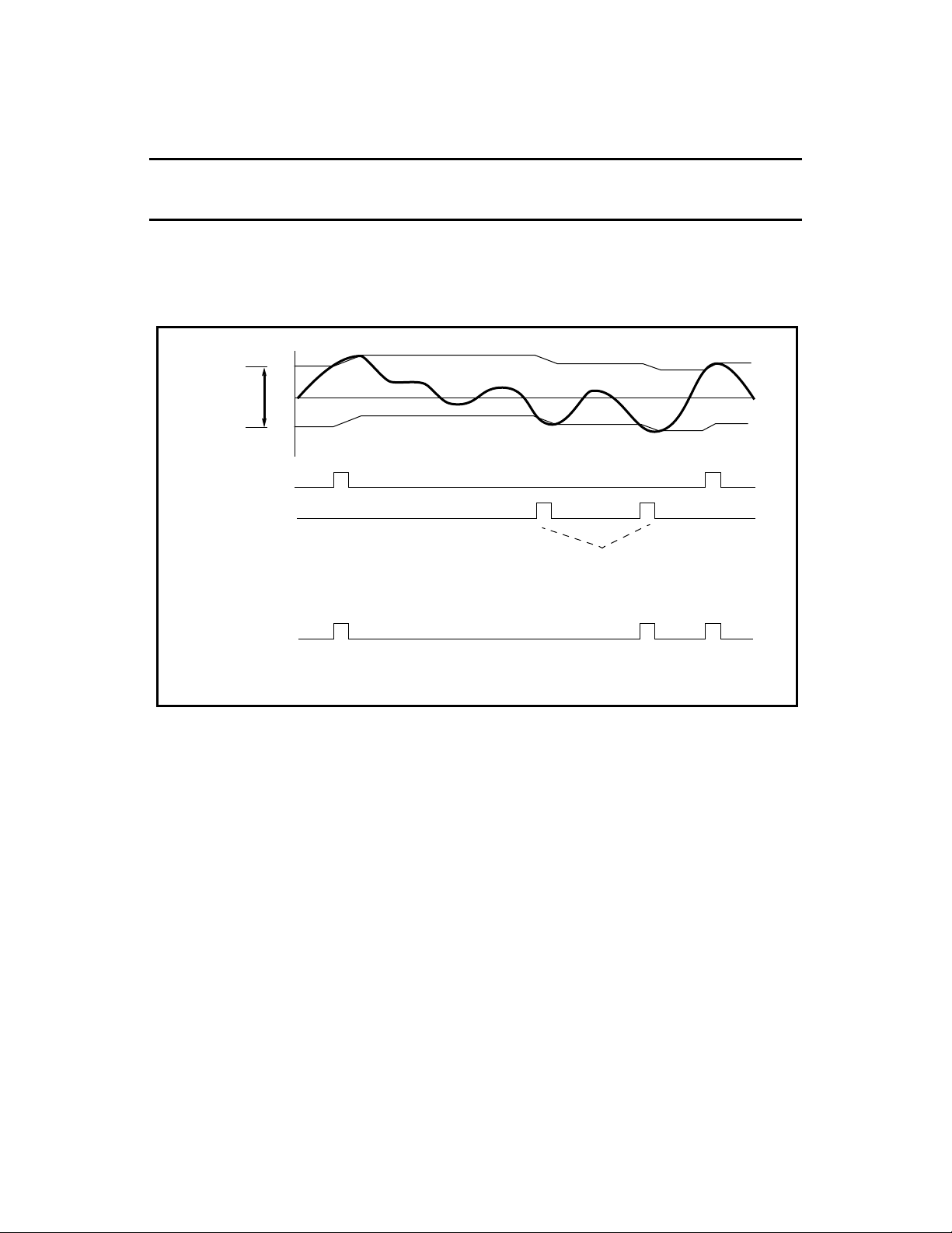
Figure 1: AGC Timing (Internal) Diagrams - Power-On Mode
PDWN
AGC
INPUT
AGC LOWZ
FAST FILTER
OFFSET RECOVERY
AGC HOLD
AGC SQUELCH
AGC FAST RECOVERY
(ATTACK & DECAY)
AGC ULTRA
FAST RECOVERY
(DECAY)
t
LZ
Power-on gain recovery
AGC
OUTPUT
100%
125%
NORMAL
ATTACK
+
-
ULTRA
FAST
DECAY
t
LZ
t
LZ
t
FR
t
LZ
POWERED UP
FAST
ATTACK
Ultra fast decay current is disabled when signal is greater
than 125% of nominal.
PRML Read Channel with PR4,
P32P4911A
8/9 ENDEC, FWR Servo
same in both of the P32P4911A's AGC control modes. In internally timed mode, the LOWZ, FASTREC, and HOLD input
pins are logically OR'ed with their respective internal control signals but do not affect the internal sequencing of the
one-shot generated AGC control signals.
1996 Jul 25 8
Philips Semiconductors Product specification
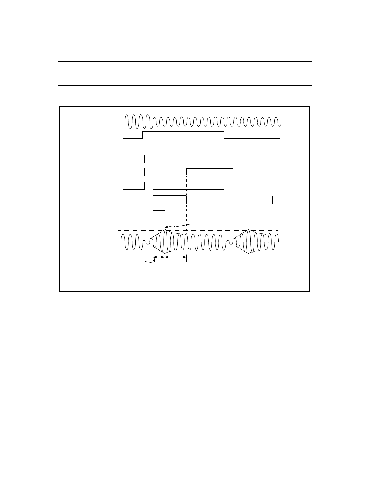
Figure 2: AGC Timing Diagrams - Servo Mode
Servo mode gain recovery
SG
AGC
INPUT
AGC OUTPUT
100%
125%
ULTRA
FAST
DECAY
+
-
AGC LOWZ
FAST FILTER
OFFSET RECOVERY
AGC HOLD
SQUELCH
AGC FAST RECOVERY
(ATTACK & DECAY)
AGC ULTRA
FAST RECOVERY
(DECAY)
t
LZ
t
FR
t
LZ
t
LZ
FAST
ATTACK
t
FR
Ultra fast decay current is disabled when
signal is greater than 125% of nominal.
PRML Read Channel with PR4,
8/9 ENDEC, FWR Servo
P32P4911A
1996 Jul 25 9
Philips Semiconductors Product specification
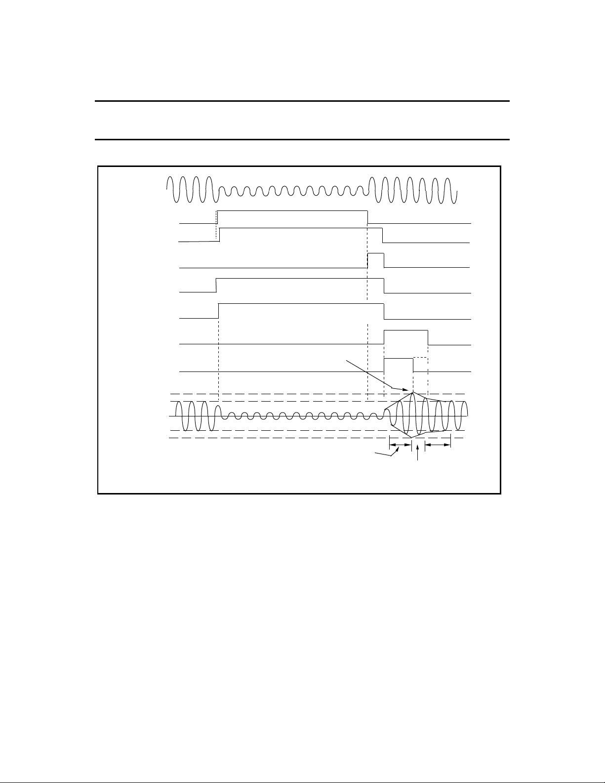
Figure 3: AGC Timing Diagrams - Write Mode
Write mode gain recovery
SG
AGC
INPUT
AGC
OUTPUT
100%
125%
ULTRA
FAST
DECAY
NORMAL
ATTACK
+
-
AGC LOWZ
FAST FILTER
AGC HOLD
AGC SQUELCH
AGC FAST RECOVERY
OFFSET RECOVERY
AGC ULTRA
FAST RECOVERY
t
LZ
t
LZ
(ATTACK & DECAY)
(DECAY)
FAST
ATTACK
t
FR
Ultra fast decay current is disabled when
signal is greater than 125% of nominal.
PRML Read Channel with PR4,
8/9 ENDEC, FWR Servo
P32P4911A
1996 Jul 25 10

Philips Semiconductors Product specification
PRML Read Channel with PR4,
P32P4911A
8/9 ENDEC, FWR Servo
Pulse Qualification Circuit Descriptions
This device utilizes three different types of pulse qualification, one exclusively for servo reads, one primarily for servo
reads, and the other for data reads.
SERVO READ MODE
For servo gray code reads, either a dual level (window type) qualifier or a hysteresis type level qualifier may be selected.
If the PDM bit in the Servo Filter Cutoff Register is set to 0, then the window qualifier is selected, and if the PDM bit is a
1, the hysteresis qualifier is selected. The polarity of the RDS/RDS is selected by the SMS bit (Servo Mode Select) in
the Data Rate Register. If SMS=0 then RDS is active-Low and if SMS=1 then RDS is active-High.
DUAL LEVEL (WINDOW) QUALIFIER
During servo reads (SG High) a dual level type of pulse qualifier is used. The level qualification thresholds are set by a
6-bit DAC which is controlled by the Servo Level Threshold Register (LDS). The register value is relative to the peak
voltage at the output of the continuous time filter, derived off of the same reference voltage internal to the chip. The
positive and negative thresholds are equal in magnitude. The state of the adaptive threshold level enable (ALE) bit in
the WP/LT Register does not affect this DAC's reference. The RDS/RDS and the PPOL outputs of the level qualifier
indicate a qualified servo pulse and the polarity of the pulse, respectively. The RDS/RDS and PPOL outputs are only
active when the SG input is High.
HYSTERESIS QUALIFIER
The hysteresis qualifier performs the same as the window qualifier except that the hysteresis qualifier guarantees that
the second of two consecutive pulses of the same polarity will not be qualified. The hysteresis qualifier will only qualify
pulses of alternating polarity.
DATA READ MODE
In data read mode (RG High), the dual level qualifier used for servo reads, is used during VCO sync field counting. Its
qualification thresholds are set by a 6-bit DAC which is controlled by the Data Level Threshold Register (LD). The
register value is relative to the peak voltage at output of the continuous time filter and the DAC both referenced to band
gap voltage. The positive and negative thresholds are equal in magnitude. The state of the adaptive threshold level
enable (ALE) bit in the WP/LT Register does not affect the DAC's reference until the sync field count has been achieved.
The RDS/RDS and the PPOL outputs of the level qualifier are not active in data read mode.
VITERBI QUALIFIER
The second type of pulse qualification, the Viterbi qualifier, is only used during data read mode after the sync field count
has been achieved. The Viterbi qualifier has two significant blocks, one that feeds the other. The first block is the
sampled pulse detector and the second is the survival sequence register.
The sampled pulse detector performs the pulse acquisition/detection in the sampled domain. It acquires pulses by
comparing the code clock sampled analog waveform to the positive and negative thresholds established by the
programmable Viterbi threshold window. The threshold window is defined to be the difference between the positive and
negative threshold levels. The threshold window, Vth, is set by a 7-bit DAC which is controlled by the Viterbi Detector
Threshold Register (VDT). While the window size is fixed by the programmed Vth value, the actual positive and negative
thresholds track the most positive and the most negative samples of the equalized input signal. For example, the Viterbi
positive signal threshold, Vpt = Vpeak (+) max if the previous detected level was (+). If the previous detect level was (-),
Vpt = Vpeak(-)max + Vth, where Vpeak(-)max is the maximum amplitude of the previously detected negative signal.
Normally Vth is set to equal Vpeak (approx. 500 mV).
After the pulses have been detected they must be further qualified by the survival sequence registers and associated
logic. This logic guarantees that for sequential pulses of the same polarity within the maximum run length, only the latest
is qualified. In this way, only the pulse of greatest amplitude will be qualified.
1996 Jul 25 11
Philips Semiconductors Product specification
Figure 4: Viterbi Detection
Viterbi
Threshold
WIndow
Viterbi
Detector
Output
+ pulse detect
- pulse detect
For sequential pulses of the same
polarity, the latest is selected by the
survival sequence register logic since
it is always of greater magnitude.
+th
-th
PRML Read Channel with PR4,
P32P4911A
8/9 ENDEC, FWR Servo
The Viterbi qualifier is implemented as two parallel qualifiers that operate on interleaved samples. Each qualifier has a
survival sequence register length of 5.
To facilitate media scan testing, the Viterbi survival sequence register may be bypassed by setting the BYPSR bit in the
Viterbi Detector Threshold (VDT) register.
Programmable Filter Circuit Description
The on-chip, continuous time, low pass filter has register programmable cutoff and boost settings, and provides both
normal and differentiated outputs. It is a 7th order filter that provides a 0.05°phase equiripple response. The group delay
is relatively constant up to twice the cutoff frequency. For pulse slimming two zero programmable boost equalization is
provided with no degradation to the group delay performance. The differentiated output is created by a single-pole,
single-zero differentiator. Both the boost and the filter cutoff frequency for data reads and the filter cutoff frequency for
servo reads are programmed through internal 7-bit DACs, which are accessed via the serial port logic. The nominal
boost range at the cutoff frequency is 0 to 13 dB for data reads and is controlled by the Data Boost Register. In servo
mode, the boost can be programmed in 2 dB steps from 0 to 6 dB by programming the two FBS bits (bits 6 and 7) in the
Filter Boost Servo register. The cutoff frequency, ƒc is variable from 4 to 34 MHz and controlled by the Data Cutoff
Register or Servo Cutoff Register in the servo mode. The cutoff and boost values for servo reads are automatically
switched when servo mode is entered.
The filter zero locations can be programmed asymmetrically about zero to compensate for MR head time asymmetry.
The asymmetry is adjusted by programming the 6 FGD bits (bits 0-5) in the Filter Boost Servo register. The asymmetric
zeros are not usable while in servo mode.
The normal low pass filter is of a seven-pole two-real-zero type. Figure 5 illustrates the transfer function normalized to
1 rad/s. The response can be denormalized to the cutoff frequency of ƒc (Hz) by replacing s by s/2πƒc, while the boost
and group delay equalization are controlled by varying the α and β.
1996 Jul 25 12
Philips Semiconductors Product specification
SM00010
IN
s2–s+1.31703
s2+1.68495s+1.31703
2.95139
s
2
+1.54203s+2.95139
5.37034
s
2
+1.14558s+5.37034
0.86133
s+0.86133
s
s+0.86133
Normal
Differential
Figure 5: Programmable Filter Normalized Transfer Function
PRML Read Channel with PR4,
P32P4911A
8/9 ENDEC, FWR Servo
With a zero at the origin, the filter provides a time-differentiated filter output. This is used in time qualification of the peak
detection. To ease the timing requirement in peak detection of a signal slightly above the qualification threshold, the
time-differentiated output is purposely delayed by 1.2 ns relative to the normal low pass output.
The normal low pass output feeds the data qualifier (DP/DN), and the differentiated output feeds the clock comparator
(CP/CN).
Five definitions are introduced for the programmable filter control discussion (Figure 6):
Cutoff Frequency: The cutoff frequency is the -3 dB low pass bandwidth with no boost and group delay equalization, i.e.
α=0 and β=0.
Actual Boost: The amount of peaking in magnitude response at the cutoff frequency due to α≠0 and/or β≠0.
Alpha Boost: The amount of peaking in magnitude response at the cutoff frequency due toα≠0 and without group delay
equalization. In general, the actual boost with group delay equalization is higher than the alpha boost. However, with
>3 dB alpha boost, the difference is minimal. α=1.31703 x (10
Group Delay ∆%: The group delay ∆% is the percentage change in absolute group delay at DC with respect to that
without equalization applied (β=0). β=0.04183 * GD%.
Group Delay Variation: The group delay variation is the change in group delay from DC to the cutoff frequency. This
can be expressed as a percentage defined as: (change in group delay ÷ absolute group delay with β=0) * 100%. An
alternative is to express the group delay variation in nanoseconds. Because the absolute group delay variation in
nanoseconds is scaled by the programmed cutoff frequency, the percentage expression is used in this specification.
BOOST(dB)/20
-1)
1996 Jul 25 13
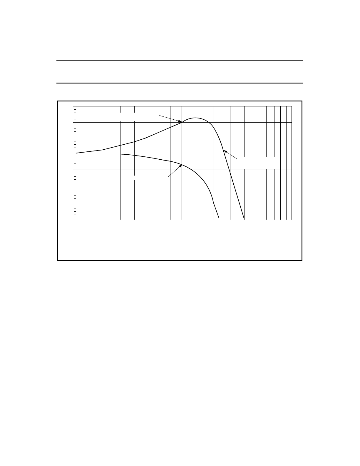
Philips Semiconductors Product specification
Figure 6: Filter Magnitude Response
Frequency (MHz)
Magnitude (dB)
SM00011
15
10
5
0
–5
–10
–15
–20
1 10 100
Cutoff = 10MHz (i) 0dB Alpha Boost & 0% Group Delay Change
(ii) 13dB Alpha Boost & +30% Group Delay Change
–3dB Cutoff Frequency
Actual Boost, same as Alpha Boost with 0%
Group Delay Change or Alpha Boost is large
Actual –3dB Bandwidth
with Boost & Group
Delay Equalization
(i)
(ii)
PRML Read Channel with PR4,
8/9 ENDEC, FWR Servo
P32P4911A
1996 Jul 25 14

Philips Semiconductors Product specification
Figure 7: Filter Group Delay Response
70
1 10 100
Cutoff = 0MHz (i) 0dB Alpha Boost & 0% Group Delay Change
(ii) 13dB Alpha Boost & +30% Group Delay Change
DC Group Delay Change
Programmable from
–30% to +30%
(i)
(ii)
1
65
60
55
50
45
40
Group Delay Variation from
‘DC’ to Cutoff Frequency
PRML Read Channel with PR4,
8/9 ENDEC, FWR Servo
Absolute Group Delay (ns)
P32P4911A
Frequency (MHz)
SM00012
FILTER OPERATION
Direct coupled differential signals from the AGC amplifier output are applied to the filter. The programmable bandwidth
and equalization characteristics of the filter are controlled by 3 internal DACs. The registers for these DACs (FC, FB,
and FGD) are programmed through the serial port. The current reference for the DACs is set using a single external
resistor connected from pin VRX to ground. The voltage at pin VRX is proportional to absolute temperature (PTAT),
hence the current for the DACs is a PTAT reference current. This establishes the excellent temperature stability for the
filter characteristics.
The cutoff frequency can be set independently in the servo mode and the data mode. In the data mode, the cutoff
frequency is controlled by the Data Cutoff Register. In the servo mode, the cutoff frequency is controlled by the Servo
Cutoff Register.
CUTOFF CONTROL
The programmable cutoff frequency from 4 to 34 MHz is set by the 7-bit linear FC DAC. The FC register holds the 7-bit
DAC control value. The cutoff frequency is set as:
ƒc (MHz) = 0.301 * FC - 1.142 44 ≤ FC ≤ 117
for servo zones
ƒc (MHz) = 0.277 * FCS + 0.08 14 ≤ FCS ≤ 43
The filter cutoff (ƒc) is defined as the -3 dB bandwidth with no boost applied. When boost/equalization is applied, the
actual -3 dB point will move out. The ratio of the actual -3 dB bandwidth to the programmed cutoff is tabulated in
Table 1 as a function of applied boost and group delay equalization.
1996 Jul 25 15

Philips Semiconductors Product specification
PRML Read Channel with PR4,
P32P4911A
8/9 ENDEC, FWR Servo
Table 1: Ratio of Actual -3dB Bandwidth to Cutoff Frequency
Alpha Boost
0 dB 1.62 1.47 1.31 1.16 1.06 1.01 1.00
1 1.74 1.62 1.50 1.38 1.28 1.21 1.19
2 1.87 1.79 1.71 1.63 1.56 1.51 1.49
3 2.01 1.96 1.91 1.87 1.83 1.80 1.79
4 2.14 2.11 2.09 2.07 2.05 2.04 2.03
5 2.25 2.24 2.23 2.22 2.21 2.20 2.20
6 2.35 2.34 2.34 2.33 2.33 2.32 2.32
7 2.44 2.44 2.43 2.43 2.42 2.42 2.42
8 2.52 2.52 2.51 2.51 2.51 2.51 2.51
9 2.59 2.59 2.59 2.59 2.59 2.59 2.59
10 2.67 2.66 2.66 2.66 2.66 2.66 2.66
11 2.73 2.73 2.73 2.73 2.73 2.73 2.73
12 2.80 2.80 2.80 2.80 2.80 2.80 2.80
13 2.87 2.87 2.86 2.86 2.86 2.86 2.86
BOOST CONTROL
The programmable alpha boost from 0 to 13 dB is set by the 7-bit linear FB DAC in data mode or 2-bit linear FBS DAC
in servo mode. The FB register holds the 7-bit DAC control value and the FBS register holds the 2-bit control value. The
alpha boost in data mode is set as:
Alpha Boost (dB) = 20 log [0.021848 * FB + 0.000046 * FC * FB + 1] 0 ≤ FB ≤ 127
The alpha boost in servo mode is set as:
Alpha Boost (dB) = 2 * FBS 0 ≤ FBS ≤ 3
That is, the boost in servo mode can be changed in 2 dB steps from 0 to 6 dB.
The programmed alpha boost is the magnitude gain at the cutoff frequency with no group delay equalization. When finite
group delay equalization is applied, the actual boost is higher than the programmed alpha boost. However, the difference
becomes negligible when the programmed alpha boost is >3 dB. Table 2 tabulates the actual boost as a function of the
applied alpha boost and group delay equalization.
±30% ±25% ±20% ±15% ±10% ±5% ±0%
Group Delay %
1996 Jul 25 16

Philips Semiconductors Product specification
PRML Read Channel with PR4,
P32P4911A
8/9 ENDEC, FWR Servo
Table 2: Ratio of Actual -3dB Bandwidth to Cutoff Frequency
Alpha Boost
0 dB 2.81 2.12 1.47 .89 0.42 0.11 0.00
1 3.36 2.76 2.21 1.72 1.33 1.09 1.00
2 3.97 3.45 2.99 2.58 2.27 2.07 2.00
3 4.63 4.19 3.80 3.47 3.21 3.05 3.00
4 5.34 4.97 4.65 4.38 4.17 4.04 4.00
5 6.10 5.79 5.52 5.30 5.14 5.03 5.00
6 6.89 6.64 6.42 6.24 6.11 6.03 6.00
7 7.72 7.51 7.34 7.19 7.09 7.02 7.00
8 8.58 8.41 8.27 8.15 8.07 8.02 8.00
9 9.47 9.33 9.22 9.12 9.05 9.01 9.00
10 10.4 10.3 10.2 10.1 10.1 10.0 10.0
11 11.3 11.2 11.1 11.1 11.0 11.0 11.0
12 12.2 12.2 12.1 12.1 12.0 12.0 12.0
13 13.2 13.1 13.1 13.1 13.0 13.0 13.0
GROUP DELAY EQUALIZATION
The group delay∆% can be programmed between -30% to +30% by the 6-bit linear FGD DAC. The FGD register holds
the 6-bit DAC control value. The group delay ∆% is set as:
Group Delay ∆% = 0.9783 * (FGD4:0) - 0.665 0 ≤ FGD4:0 ≤ 31 and FGD5 = sign bit
The group delay ∆% is defined to be the percentage change of the absolute group delay due to equalization from the
absolute group delay without equalization at DC.
The current reference for the filter DACs is set using a single 12.1 kΩ resistor, from the VRX pin to ground. The voltage
at VRX is proportional-to-absolute-temperature (PTAT).
The outputs of the filter are internally AC coupled to the qualifier inputs and buffers for the filter monitoring test points
TPC+/TPC- and TPD+/TPD-.
±30% ±25% ±20% ±15% ±10% ±5% ±0%
Group Delays ∆%
Internal AC Coupling
The conventional external ac coupling at the filter to qualifier interface has been replaced by a pair of feedback circuits,
one for the normal and one for the differentiated outputs of the filter. The offset of the filter outputs are sensed, integrated,
and fed back to the filter output stage. The feedback loop forces the filter offset nominally to zero. In the normal read
mode, (LOWZ=0), the integration time constant is set to 5 µs until the sync field counter reaches the programmed SFC
count. At the SFC count, the offset sensing is switched into sampled mode and the time constant is reduces to 300 ns.
In sampled mode the offset correction voltage is generated from the zeros qualified by the quantizer. This ensures that
the sampled voltage level, not DP/DN, will be offset free.
1996 Jul 25 17

Philips Semiconductors Product specification
PRML Read Channel with PR4,
P32P4911A
8/9 ENDEC, FWR Servo
Amplitude Asymmetry Detection and Correction
In the presence of amplitude asymmetry, such as that generated by MR heads, the sampled data processor (SDP) will
be presented with zeros generated in one of two ways. The first is due the lack of a magnetic transition and will be
referred to as a "real" zero. The second is produced by the superposition of adjacent +1 and -1 magnetic transitions and
results in zero samples that shall be referred to as "cancelled" zeros. In the presence of amplitude asymmetry from an
MR head, the "real" zeros are zero, but the "cancelled" zeros are offset by the difference between the +1 and -1 samples.
The offset correction circuit forces the ground reference of the sampled data processor to the center of the "real" and
"cancelled" zero sample levels.
The integration time constant is increased by a factor of 4 to 1.0 µs, after the sync byte has been detected.
AMPLITUDE ASYMMETRY MONITOR POINT
An amplitude asymmetry quality factor "Qasym" may be selected to be output on the ATO output pin by programming
the ASEL bits in the Power Down Register. This signal is derived by computing the average distance of the "real" and
"canceled" zeros from the sampled data processor's system ground which was established between the two zeros levels
by the offset correction circuit. The average distance is a measure of the asymmetry present in the MR read back signal.
A gain of 4 from the sampled values is utilized and is low pass filtered with a time constant that is programmable to one
of four different values by programming the two QTC bits in the Control Operating Mode Register #2.
The signal is then buffered and differentially multiplexed to the ATO pin. The signal is referenced to MAXREF/2.
The asymmetry quality factor can be held at the value present at sync byte detect by setting the FREZQ bit in the WP/LT
Register. The value will be held for 10 ms and is NOT reset. The ATO output may also be externally filtered to provide
time constants that are appropriate for averaging over major portions of, or an entire sector. The capacitors on externally
added filters must be externally reset. Note that any external filtering added to ATO output pin will affect both the
amplitude asymmetry monitor signal and the equalization quality monitor signal since they are both muxed to the ATO
output pin.
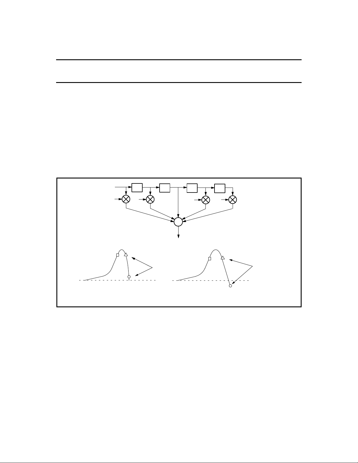
Adaptive Equalizer Circuit Description
Up to 7 dB of equalization for fine shaping of the incoming read signal to the PR4 waveshape is provided by a 5 tap,
sampled analog, transversal filter. This filter provides a self adaptive multiplier coefficient for the inner taps and a
programmable coefficient for the outer taps. Both inner taps use the same coefficient (km1), and both outer taps use the
same coefficient (km2).
For the adaptive inner taps, the value of km1 is adjusted to force "zero" samples to zero volts. A special equalizer training
pattern, located after the VCO sync field in the sector format, is used to provide an optimum signal for the equalizer to
adapt to. The adaptive property of these taps is enabled or disabled by the AEE bit in the Sample Loop Register. If the
adaptive property is enabled, whether adaptation occurs only during the training pattern or both during the training
pattern and the user data is controlled by the AED bit in the Sample Loop Register.
The adaptation can be observed when the equalizer control voltage is selected as the TPA+/TPA- output. The equalizer
control voltage is approximately related to km1 by:
km1 = 0.009 * Date Rate (Mbit/s) * (TPA+ - TPA-)
The multiplier coefficients for the adaptive taps can be held for up to 10 ms if the EQHOLD input is brought High after
sync byte detect has occurred during a previous read in which proper training has occurred. The EQHOLD input pin may
be asserted at any time during a read cycle and the adaptive coefficient Km1 present at that time will be held, provided
no leakage occurs, until the EQHOLD input is de-asserted.
The multiplier coefficient, km2, for the outer taps is programmable between +0.117 and -0.135 by the 4 km bits (bits 4-7)
in the Control Operating Mode Register #2
1996 Jul 25 18
.
Philips Semiconductors Product specification
Figure 8: Block Diagram of 5-Tap Equalizer
yn = k
m2
xn + k
m1
x
n-1
+ x
n-2
+ km1 x
n-3
+ km2 x
n-4
need more boost
decrease km
need less boost
increase km
+1
+1
+1
+1
0
0
0V 0V
D
D
D
D
S
x
n
x
n-1
x
n-2
x
n-3
x
n-4
k
m2
k
m1
k
m1
k
m2
y
n
km1 coefficient adapts to force ’0’ samples to 0V
SM00026
PRML Read Channel with PR4,
P32P4911A
8/9 ENDEC, FWR Servo
EQUALIZATION QUALITY MONITOR POINT
An equalization quality factor "Q" may be selected to be output on the ATO output pin by programming the ATOSEL bits
in the Power Down Register and should be used as a guide for selection of the appropriate value for km2. This signal is
derived by computing the absolute distance of the "real" and "canceled" zeros from the sampled data processor's system
ground which was established between the two zeros levels by the offset correction circuit. Then the asymmetry factor
(QASYM) is subtracted and the resulting signal is full wave rectified and low pass filtered using one of the four time
constants that may be programmed with the two QTC bits in the Control Operating Mode Register #2. The signal is then
buffered and differentially multiplexed to the ATO pin. The overall gain to the ATO pin is 4. The signal is referenced to
MAXREF/2.
The equalization quality factor can be held at the value present at sync byte detect by setting the FREZQ bit in the WP/LT
Register. The value will be held for approx. 10 ms and is NOT reset. The ATO output may also be externally filtered to
provide time constants that are appropriate for averaging over major portions of, or an entire sector. The capacitors on
externally added filters must be externally reset.
Time Base Generator Circuit Description
The time base generator (TBG) is a PLL based circuit, that provides a programmable reference frequency to the data
separator for constant density recording applications. This time base generator output frequency can be programmed
with a less than 1% accuracy via the M, N and DR Registers. The TBG output frequency, Fout, should be programmed
as close as possible to ((9/8) * NRZ Data Rate). The time base also supplies the timing reference for write
precompensation so that the precompensation tracks the reference time base period.
The time base generator requires an external passive loop filter to control its PLL locking characteristics. This filter is
fully-differential and balanced in order to reduce the effects of common mode noise.
In read, write and idle modes, the programmable time base generator is used to provide a stable reference frequency for
the data separator. In the write and idle modes, the Time Base Generator output, when selected by the Control Test
Mode Register, can be monitored at the TPB+ and TPB- test pins. In the read mode, the TBG output should not be
selected for output on the test pins so that the possibility of jitter in the data separator PLL is minimized.
1996 Jul 25 19
 Loading...