

Philips OQ2541BHP, OQ2541BU DATASHEETS

INTEGRATED CIRCUITS
DATA SH EET
OQ2541BHP; OQ2541BU
SDH/SONET data and clock
recovery unit STM1/4/16
OC3/12/48 GE
Product specification
File under Integrated Circuits, IC19
2000 Sep 18

Philips Semiconductors Product specification
SDH/SONET data and clock recovery unit
STM1/4/16 OC3/12/48 GE
FEATURES
• Data and clock recovery up to 2.5 Gbits/s
• Multirate configurable (155, 622, 1250 or 2500 Mbits/s)
• Full ITU-T jitter compliance (G.958 and G.813)
• Full Bellcore jitter compliance
• Differential data input with 2.5 mV (p-p) typical
sensitivity
• Differential Current-Mode Logic (CML) data and clock
outputs with 50 Ω driving capability
• Adjustable CML output level
• Bypass mode for non SDH/SONET or Gigabit
Ethernet (GE) bit rates
• Loop mode for system testing
• Bit Error Rate (BER) related Loss Of Signal (LOS)
detection
• Few external components needed
• Single supply voltage
• Power dissipation 400 mW (typical value)
• LQFP48 plastic package.
DESCRIPTION
TheOQ2541B is a data and clock recovery ICintended for
use in Synchronous Digital Hierarchy (SDH) and
Synchronous Optical Network (SONET) systems. The
circuit recovers data and extracts the clock signal from an
incoming bitstream up to 2.5 Gbits/s.
The OQ2541B can be configured for use in STM1/OC3,
STM4/OC12, STM16/OC48 and GE systems, with full
ITU-T G.958 and G.813 jitter compliance, or Bellcore jitter
compliance, whichever is applicable. The OQ2541B also
features a bypass mode, for non SDH/SONET or
GE bit rates, in which the clock recovery function is
bypassed.
OQ2541BHP; OQ2541BU
APPLICATIONS
• Data and clock recovery in STM1/OC3, STM4/OC12
and STM16/OC48 transmission systems
• Data and clock recovery in GE transmission systems
• Regenerator and repeater applications
• Wavelength conversion regenerator in Dense
Wavelength Division Multiplexing(D)WDM applications.
ORDERING INFORMATION
TYPE
NUMBER
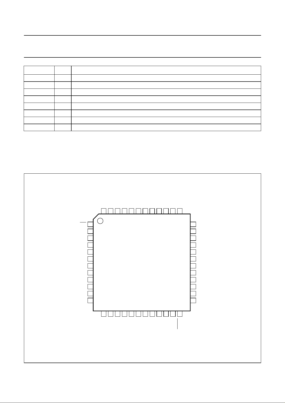
OQ2541BHP LQFP48 plastic low profile quad flat package; 48 leads; body 7 × 7 × 1.4 mm SOT313-2
OQ2541BU − bare die; 2360 × 2360 × 380 µm −
NAME DESCRIPTION VERSION
PACKAGE
2000 Sep 18 2

Philips Semiconductors Product specification
SDH/SONET data and clock recovery unit
STM1/4/16 OC3/12/48 GE
BLOCK DIAGRAM
handbook, full pagewidth
LOS
39
33
DIN
DINQ
CREF
CREFQ
34
21
22
ALEXANDER
PHASE
DETECTOR
enable
FREQUENCY
WINDOW
DETECTOR
(1000 ppm)
DOUT1250
+
DOUT622
DOUT155
27
28
FREQUENCY
DIVIDER 1
1/2/4/16
OQ2541B
∫ dt
OQ2541BHP; OQ2541BU
AREF
ENL
30
proportional
path
integrating
path
48
DATA
AND
CLOCK
OUTPUT
VCRO
2.5 GHz
1
24
ALLON
42
DOUT
43
DOUTQ
45
COUT
46
COUTQ
6
DLOOP
7
DLOOPQ
3
CLOOP
4
CLOOPQ
10
BYPASS
5
i.c.
13, 18, 19,
36, 40
16
2, 5, 8, 11, 14, 17, 20
23, 26, 29, 32, 35, 38
41, 44, 47
GND
FREQUENCY
DIVIDER 2
64/128
12 25
9
DREF19LOCK
Fig.1 Block diagram.
2000 Sep 18 3
CAPDOQ
CAPUPQ
130 pF130 pF
1516
POWER
CONTROL
V
EE1
V
EE2
31
37
MGT203
PC

Philips Semiconductors Product specification
SDH/SONET data and clock recovery unit
STM1/4/16 OC3/12/48 GE
PINNING
SYMBOL PIN DESCRIPTION
ENL 1 loop mode enable input (active LOW)
GND 2 ground; note 1
CLOOP 3 clock output in loop mode (differential)
CLOOPQ 4 inverted clock output in loop mode (differential)
GND 5 ground; note 1
DLOOP 6 data output in loop mode (differential)
DLOOPQ 7 inverted data output in loop mode (differential)
GND 8 ground; note 1
DREF19 9 reference frequency select input 1 (see Table 2)
BYPASS 10 data recovery and clock extraction bypass mode input
GND 11 ground; note 1
LOCK 12 phase lock detection output
i.c. 13 internally connected; note 2
GND 14 ground; note 1
CAPUPQ 15 external loop filter capacitor connection
CAPDOQ 16 external loop filter capacitor return connection
GND 17 ground; note 1
i.c. 18 internally connected; note 2
i.c. 19 internally connected; note 2
GND 20 ground; note 1
CREF 21 reference clock input (differential)
CREFQ 22 inverting reference clock input (differential)
GND 23 ground; note 1
ALLON 24 enable all outputs (input active LOW)
V
EE1
GND 26 ground; note 1
DOUT1250 27 STM mode select input 1 (see Table 3)
DOUT622 28 STM mode select input 2 (see Table 3)
GND 29 ground; note 1
DOUT155 30 STM mode select input 3 (see Table 3)
V
EE2
GND 32 ground; note 1
DIN 33 data input (differential)
DINQ 34 inverting data input (differential)
GND 35 ground; note 1
i.c. 36 internally connected; note 2
PC 37 control output for negative power supply
GND 38 ground; note 1
LOS 39 loss of signal detection output
i.c. 40 internally connected; note 2
25 negative supply voltage (−3.3 V); note 3
31 negative supply voltage (−3.3 V); note 3
OQ2541BHP; OQ2541BU
2000 Sep 18 4
Philips Semiconductors Product specification
SDH/SONET data and clock recovery unit
OQ2541BHP; OQ2541BU
STM1/4/16 OC3/12/48 GE
SYMBOL PIN DESCRIPTION
GND 41 ground; note 1
DOUT 42 data output in normal mode (differential)
DOUTQ 43 inverted data output in normal mode (differential)
GND 44 ground; note 1
COUT 45 clock output in normal mode (differential)
COUTQ 46 inverted clock output in normal mode (differential)
GND 47 ground; note 1
AREF 48 reference voltage input for controlling voltage swing on data and clock outputs
Notes
1. All GND pins or pads must be bonded; do not leave one single GND pin or pad unconnected.
2. All pins or pads denoted ‘i.c.’ should not be connected. Connections to these pins or pads degrade device
performance.
3. All VEE pins or pads must be bonded; do not leave one single VEE pin or pad unconnected.
handbook, full pagewidth
ENL
GND
CLOOP
CLOOPQ
GND
DLOOP
DLOOPQ
GND
DREF19
BYPASS
GND
LOCK
COUTQ
GND
47
14
GND
COUT
46
45
15
16
CAPUPQ
CAPDOQ
GND
44
OQ2541BHP
17
GND
AREF
48
1
2
3
4
5
6
7
8
9
10
11
12
13
i.c.
DOUT
DOUTQ
43
42
18
19
i.c.
i.c.
GND
41
20
GND
i.c.
40
21
CREF
GND
LOS
39
38
22
23
GND
CREFQ
PC
24 37
ALLON
36
i.c.
35
GND
34
DINQ
33
DIN
32
GND
V
31
DOUT155
30
29
GND
DOUT622
28
27
DOUT1250
26
GND
V
25
MGT204
EE2
EE1
Fig.2 Pin configuration.
2000 Sep 18 5

Philips Semiconductors Product specification
SDH/SONET data and clock recovery unit
STM1/4/16 OC3/12/48 GE
FUNCTIONAL DESCRIPTION
The OQ2541B recovers data and clock signals from an
incoming high speed bitstream. The input signal on
pins DIN and DINQ is buffered and amplified by the input
circuit(seeFig.1). The signal is then fed into theAlexander
phase detector, where the phase of the incoming data
signal is compared with that of the internal clock. If the
signals are out of phase, the phase detector generates
correction pulses (up or down) that shift the phase of the
Voltage Controlled Ring Oscillator (VCRO) output in
discrete amounts (∆ϕ) until the clock and data signals are
in phase. The technique used is based on principles first
proposed by J.D.H. Alexander, hence the name of the
phase detector.
Data sampling
The eye pattern of the incoming data is sampled at three
instants A, T and B (see Fig.3). When clock and data
signals are synchronized (locked):
• A is the centre of the data bit
• T is in the vicinity of the next transition
• B is in the centre of the bit following the transition.
If the same level is recorded at both A and B, a transition
has not occurred and no action is taken, regardless of
level T. However, if levels A and B are different, a
transition has occurred and the phase detector uses
level T to determine whether the clock was too early or too
late with respect to the data transition.
If levels A and T are the same but different from level B,
the clock was too early and needs to be slowed down a
little. The Alexander phase detector then generates a
down pulse which stretches a single output pulse from the
ring oscillator by approximately 0.25% which is 1 ps of the
400 ps bit period in the STM16/OC48 mode. This forces
the VCRO to run at a slightly lower frequency for one bit
period. The phase of the clock signal is thus shifted
fractionally with respect to the data signal.
handbook, halfpage
DATADATA
OQ2541BHP; OQ2541BU
If, on the other hand, levels B and T are the same but
different from level A, the clock was too late and needs to
be speeded up for synchronization. The phase detector
generates an up pulse, forcing the VCRO to run at a
slightly higher frequency (+0.25%) for one bit period. The
phase of the clock signal is shifted with respect to the data
signal (as above, but in the opposite direction). While
making these phase adjustments, only the proportional
pathis active. Because the instantaneous frequency of the
VCRO can be changed in one of two discrete steps only
(±0.25%), this type of loop is also known as a Bang/Bang
Phase-Locked Loop (PLL).
If not only the phase but also the frequency of the VCRO
is incorrect, a long train of up or down pulses will be
generated. This pulse train is integrated to generate a
control voltage that is used to shift the centre frequency of
the VCRO. Once the correct frequency has been
established, only the phase needs to be adjusted for
synchronization. The proportional path adjusts the phase
of the clock signal, whereas the integrating path adjusts
the centre frequency.
Frequency window detector
The frequency window detector checks the VCRO
frequency, which has to be within a 1000 ppm (parts per
million) window around the required frequency.
The detector compares the output of frequency divider 2
with the reference frequency on pins CREF and CREFQ
(19.44 or 38.88 MHz;see Table 2).Ifthe VCRO frequency
is found to be outside this window, the frequency window
detectordisablesthe Alexander phase detector and forces
the VCRO output to a frequency within the window. Then,
the phase detector starts acquiring lock again. Due to the
loosecouplingof1000 ppm,thereferencefrequency does
notneedtobe highly accurate or stable. Any crystal-based
oscillator that generates a reasonably accurate frequency
(e.g. 100 ppm) will do.
Since sampling point A is always in the centre of the eye
pattern when the data and clock signals are in phase
(locked), the values recorded at this point are taken as the
retrieved data. The data and clock signals are available at
the CML output buffers that are capable of driving a 50 Ω
load.
ATB
CLOCK
MGK143
Fig.3 Data sampling.
2000 Sep 18 6
RF data and clock input circuit
The schematic of the input circuit is shown in Fig.4.
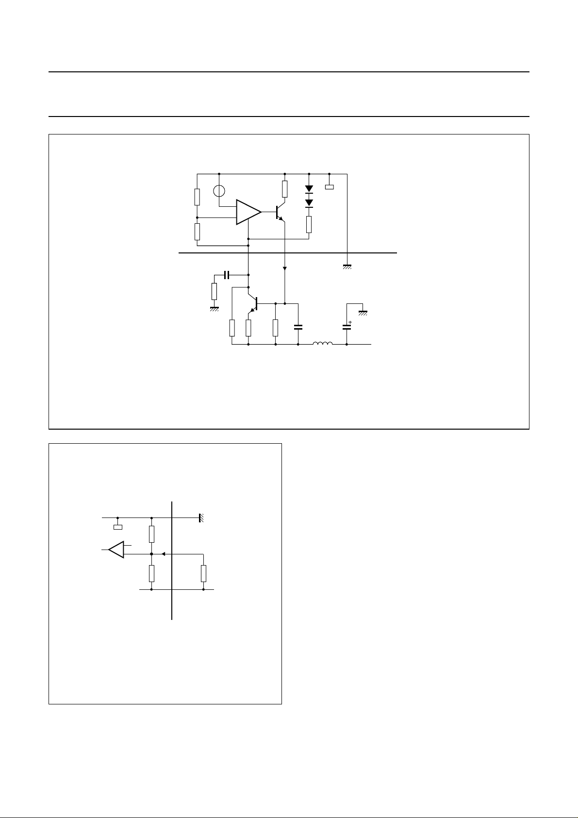
RF data and clock output circuit
The schematic of the output circuit is shown in Fig.5.
Philips Semiconductors Product specification
SDH/SONET data and clock recovery unit
STM1/4/16 OC3/12/48 GE
handbook, halfpage
50 Ω50 Ω
DIN,
CREF
VEE
DINQ,
CREFQ
MGL669
OQ2541BHP; OQ2541BU
100 Ω100 Ω
DOUTQ, COUTQ
DOUT, COUT
V
AREF
V
EE
MGL670
Fig.4 RF data and clock input circuit.
Power supply and power control loop
The OQ2541B contains an on-board voltage regulator.
An external power transistor is needed to deliver the
supply to this circuit. The required external circuit is
straightforward, and can be built using a few components.
Asuitablecircuitwithapowersupplyof−4.5 Visillustrated
in Fig.6. Do not omit the 2 Ω resistor in series with the
100 nF decoupling capacitor.
A different configuration could be used, as long as the
power supply rejection ratio is greater than 60 dB for all
frequencies. The inductor is an RF choke with an
impedance greater than 50 Ω at frequencies higher than
2 MHz. Any transistor with a β of approximately 100 and
sufficient current sink capability can be used.
The OQ2541B can also be used with a power supply of
−5.0 or −5.2 V. The only adaptation to be made to the
power control circuit is to change the emitter resistor R1
(see Table 1).
Table 1 Value of resistor R1
POWER SUPPLY RESISTOR R1
−4.5 V 6.8 Ω
−5.0 V 8.2 Ω
−5.2 V 10.0 Ω
Fig.5 RF data and clock output circuit.
Output amplitude reference
The voltage swing at the CML compatible output stages
(pins DOUT, DOUTQ, COUT, COUTQ, DLOOP,
DLOOPQ, CLOOP and CLOOPQ) can be controlled by
adjusting the voltage on pin AREF (see Fig.7). An internal
voltage divider of 500 Ω and 16 kΩ connected between
ground and VEEinitially fixes this level.
In most applications, the outputs will be DC coupled to a
50 Ω load. The output level regulation circuit will maintain
a 200 mV (p-p) single-ended swing across this load. The
voltageonpin AREF is half the single-ended peak-to-peak
value of the output signal (−100 mV). No adjustments are
necessary with DC coupling.
If the outputs are AC coupled, the voltage on pin AREF is
half the single-ended peak-to-peak value of the output
signal multiplied by a factor
RLRo+
-------------------R
L
where RLis the external load and Rois the output
impedance of the OQ2541B (100 Ω).
The resulting output amplitude with the same voltage on
pin AREF is thus different for DC and AC coupled loads.
2000 Sep 18 7
Philips Semiconductors Product specification
SDH/SONET data and clock recovery unit
STM1/4/16 OC3/12/48 GE
handbook, full pagewidth
2 Ω
100 nF
1 kΩ
BAND GAP
REFERENCE
V
EE
β ≈
R1
6.8 Ω
PC GND
100
1
kΩ
3.3
nF
OQ2541BHP; OQ2541BU
on chip
off chip
1 µF
(1)
L1
−4.5 V
MGT205
(1) L1 = RF choke type Murata BLM21 or equivalent.
Fig.6 Schematic diagram of OQ2541B power control loop.
handbook, halfpage
500 Ω
16 kΩ R
GND
AREF
V
EE
off chipon chip
V
AREF
MGL667
AREF
If the outputs are AC coupled, the formulae for calculating
the required voltage on pin AREF and the value of the
resistor connected between pins AREF and VEE are as
follows:
RLR+
V
AREF
– 0.5V
--------------------R
L
O
×=
swing
and:
R1
AREF
=
-----------------------------------------------------------1
–
R
where R1 = 500 Ω, R2 = 16 kΩ and V
V
EE
×
--------------- -
V
R1
×
------- -
R2
AREF
V
EE
--------------- V
AREF
1–
1–
= −3.3 V.
EE
To maintain a single-ended swing of 200 mV (p-p) across
a50ΩAC-coupled load, thevoltage on pin AREF must be
100 mV–
50 + 100()Ω
× 300 mV–=
--------------------------------50 Ω
Fig.7 Functionality of pin AREF.
2000 Sep 18 8
This can be achieved by connecting a 7.3 kΩ resistor
between pins AREF and VEE.
Philips Semiconductors Product specification
SDH/SONET data and clock recovery unit
STM1/4/16 OC3/12/48 GE
External capacitor for loop filter
The loop filter is an integrator with a built-in capacitance of
2 × 130 pF. To ensure loop stability while the frequency
window detector is active, an external capacitance of
360 nF (2 times 180 nF parallel) must be connected
between pins CAPUPQ and CAPDOQ.
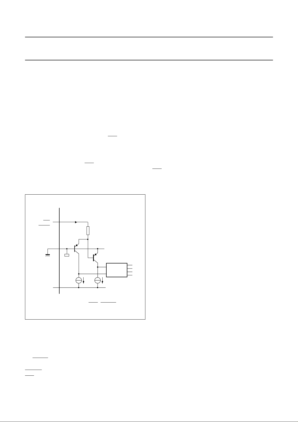
Loop mode enable
The loop mode is provided for system testing (see Fig.8).
The loop mode is enabled by applying a voltage between
−0.8 and +0.8 V (LOW-level TTL) to pin ENL. This selects
the loop mode: the outputs on pins DLOOP, DLOOPQ,
CLOOP and CLOOPQ are switched on.
If a voltage higher than 2.0 V (HIGH-level TTL) or lower
than −2.0 V is applied to pin ENL, then pins DOUT,
DOUTQ, COUT and COUTQ are switched on while
pins DLOOP, DLOOPQ, CLOOP and CLOOPQ are
disabled to minimize power consumption.
OQ2541BHP; OQ2541BU
Bypass mode
The bypass mode is provided to use the OQ2541B at non
standard SDH/SONET or GE bit rates. The data recovery
and clock extraction function can be bypassed if no clock
extraction is needed, or when the bit rate is different from
155, 622, 1250 or 2488 Mbit/s. Here, the incoming data
from DIN and DINQ is directly fed to the RF outputs. Clock
outputs COUT, COUTQ, CLOOP, CLOOPQ and the
LOS detection have no meaning in this mode.
In the bypass mode, the data and clock recovery circuit is
disabled to reduce crosstalk. The bypass mode can be
activatedby applying a voltage lower than−2.0 Vor higher
than +2.0 V to pin BYPASS. If the voltage on this pin is
between −0.8 and +0.8 V, extracted data and recovered
clock are present on the RF outputs (normal
DCR operation). The input has the same structure as the
ENL input (see Fig.8).
Lock detection
handbook, halfpage
off chip on chip
ENL,
ALLON,
BYPASS
V
EE
GND
36 kΩ
DECODER
LOGIC
MGT206
Fig.8 Input circuit of pins ENL, ALLON and
BYPASS.
All outputs active
All outputs (normal outputs DOUT, DOUTQ, COUT,
COUTQ and loop mode outputs DLOOP, DLOOPQ,
CLOOP and CLOOPQ) can be activated by applying a
voltage lower than −2.0 V or higher than +2.0 V to
pin ALLON. If the voltage on this pin is between
−0.8 and +0.8 V, the active outputs can be selected by
pin ENL. The input has the same structure as the
ENL input (see Fig.8).
Pin LOCK should be interpreted as an indication of the
presence of the reference clock on pin CREF and of the
proper functioning of the acquisition aid (frequency
window detector).
Pin LOCK is an open-collector TTL output and is to be
pulledup with a 10 kΩ resistortoa positive supply voltage.
If theVCO frequency is within a 1000 ppm window around
the desired frequency, pin LOCK will stay at a HIGH level.
If no reference clock is present, or the VCO is outside the
1000 ppm window, pin LOCK will be at a LOW level. The
logic level on pin LOCK does not indicate locking of the
PLL to the incoming data; this is indicated by the signal on
pin LOS.
Loss of signal detection
The LOS function is closely related to the functionality of
the Alexander phase detector; see Fig.3 for the meaning
of A, B and T in this section.
The functional description states that the phase detector
does not take any action if the value at sample points
A and B are the same, as there has not been any
transition. However, if levels A and B are the same but
different from level T, this still means there has not been
any transition, but level T has got the wrong level
somehow. This is probably due to noise or bad signal
integrity, which will lead to a bit error. Hence, the
occurrence of this particular situation is an indication of bit
errors. If too many of these bit errors occur per time and
thePLLisgraduallylosinglock,theLOS alarm is asserted.
The LOS alarm assert level is around BER = 5 × 10⁻²and
the de-assert level is around BER = 1 × 10⁻³.
2000 Sep 18 9

Philips Semiconductors Product specification
SDH/SONET data and clock recovery unit
STM1/4/16 OC3/12/48 GE
The LOS function will only work properly if the input signal
is larger than the input offset of the OQ2541B. Otherwise,
the signal will be masked by the input offset and
interpreted as consecutive bits of the same sign, thus
obstructing a proper LOS detection. In practice, an optical
front-enddevicewithanoiselevel (RMS value) larger than
the specified offset of the OQ2541B will ensure a proper
LOS indication.
The LOS detection is BER related, but neither dependent
on the data stream content nor protocol. Therefore, an
SDH/SONET data stream is not a prerequisite fora proper
LOS function. Since the LOS function of the OQ2541B is
derived from digital signals, it is a good supplement to an
analog, amplitude based, LOS indication.
Pin LOS is an open-collector TTL compatible output.
A pull-up resistor is to be connected to a positive supply
voltage.
The LOS pin will be ata HIGH level (TTL) ifthe data signal
is absent on pins DIN and DINQ or if BER > 5 × 10⁻².
Otherwise, pin LOS will be at a LOW level if
BER<1×10⁻³.
Reference frequency select
A reference clock signal of 19.44 or 38.88 MHz must be
connected to pins CREF and CREFQ. It should be noted
that the reference frequency should be either
39.0625 or 19.53125 MHzinaGE system.Pin DREF19is
used to select the appropriate output frequency at
frequency divider 2 (see Table 2).
To minimize the adverse influence of reference clock
crosstalk, a differential signal with an amplitude from
75 to 150 mV (p-p) is advised.
Sincethereferenceclockisonlyused as an acquisition aid
for the PLL of the frequency window detector, the quality
of the reference clock (i.e. phase noise) is not important.
There is no phase noise specification imposed on the
reference clock generator and even frequency stability
may be in the order of 100 ppm. In general, most
inexpensive crystal-based oscillators are suitable.
When the OQ2541B is used in an application with a fixed
reference clock frequency, it is best to connect
pin DREF19 through a short track or a via to the ground
plane or pin VEE. If a selectable reference clock frequency
is required in the application, the pin can be controlled
through a low ohmic switching FET, e.g. BSH103 or
equivalent (low R
DSon
).
OQ2541BHP; OQ2541BU
Table 2 Reference frequency selection
FREQUENCY
(MHz)
38.88 64 ground
19.44 128 V
STM mode selection
The VCRO has a large tuning range. However, the
performance of the OQ2541B is optimized for
SDH/SONET, including GE bit rates.
Due to the nature of the PLL, the wide tuning range is a
necessity for proper lock behaviour over the guaranteed
temperature range, aging and batch to batch spread.
Though it might seem that the OQ2541B is capable of
recovering other bit rates than SDH/SONET and
GE bit rates(STM1/OC3,STM4/OC12, STM16/OC48 and
1250 Mbits/s), the behaviour cannot be guaranteed.
The required SDH/SONET bit rate is selected by
connecting pins DOUT155, DOUT622 and DOUT1250
to ground or to the supply voltage VEE (see Table 3):
• For STM16/OC48 (2488.32 Mbits/s) operation, all three
pins have to be connected to ground
• ForGE (1250 Mbits/s) operation, pin DOUT1250 has to
be connected to V
• For STM4/OC12 (622.08 Mbits/s) operation,
pins DOUT1250 and DOUT622 have to be connected
to VEE (the dividers are daisy chained)
• ForSTM1/OC3(155,52 Mbits/s) operation, all threepins
have to be connected to VEE.
The connections to VEE and ground carry a current of a
few mA and should have low resistance and inductance.
Therefore, short printed-circuit board tracks are
recommended. In some cases, a small decoupling
capacitor (approximately 100 pF) near the selection pins
might be necessary to provide a clean return path for
RF currents.
When the OQ2541B is used in an application with a fixed
data rate, it is best to connect pins DOUT155, DOUT622
and DOUT1250throughashorttrackoraviatotheground
plane or pin VEE. If a selectable bit rate is required in the
application, the pins can be controlled through low-ohmic
switching FETs, e.g. BSH103 or equivalent (low R
DIVISION
FACTOR
EE
LEVEL ON PIN
DREF19
EE
DSon
).
2000 Sep 18 10
Philips Semiconductors Product specification
SDH/SONET data and clock recovery unit
OQ2541BHP; OQ2541BU
STM1/4/16 OC3/12/48 GE
Table 3 STM mode select
MODE
BIT RATE
(Mbits/s)
STM1/OC3 155.52 16 V
DIVISION
FACTOR
DOUT155 DOUT622 DOUT1250
EE
STM4/OC12 622.08 4 ground V
Gigabit Ethernet 1250.00 2 ground ground V
STM16/OC48 2488.32 1 ground ground ground
Application with positive supply voltage
The versatile design of the OQ2541B also allows it to
operate in a positive supply voltage application, although
somepins have a different mode of operation.This section
deals with these differences and supports the user with
achieving a successful application of the OQ2541B in a
5 V environment.
APPLICATION DIAGRAM
Fig.32 shows a sample application diagram. It should be
noted that all pins GND are now connected to VCCand all
pins VEE are connected to the regulated voltage from the
power controller.
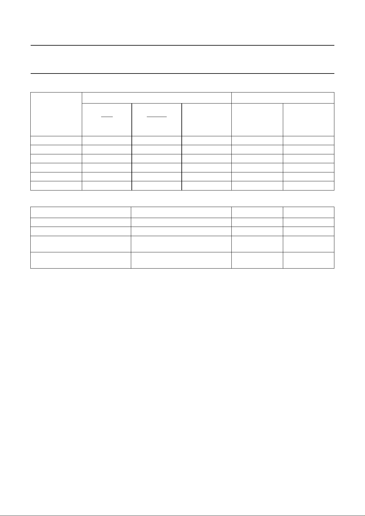
LOSS OF SIGNAL AND LOCK DETECTION
In the negative supply application, pins LOS and LOCK
are open-collector outputs that require pull-up resistors to
a positive supply voltage.
In the positive supply application, the pull-up voltage
needstobehigherthanthepositive supply voltage and the
signals on pins LOS and LOCK would no longer be
TTL compatible. However, the internal circuit on pins LOS
and LOCK can be used in a current mirror configuration
(see Fig.9). This requires only an external PNP transistor
(e.g. BC857 or equivalent) to mirror the current. A 10 kΩ
pull-down resistor from the collector of the external
transistor to ground yields a TTL compatible signal again,
albeitinverted.Table 5 shows the meaning of the LOS and
OUTPUT SELECTION
LOCK flags, when used in the positive supply application.
LEVEL ON PIN
V
EE
EE
V
EE
V
EE
EE
In a positive supply voltage application, the functions of
pins ENL, ALLON and BYPASS are different than in a
negative supply application, see also Table 4.
The functions can be activated by a voltage more than
2.0 V lower than 5.0 V (VCC). Preferably, they should be
connected to VEE (pin 25), which is approximately 3.3 V
below VCC. If the pins do not differ by more than 0.8 V
of VCC (5.0 V), the functions are deactivated.
If the pin is connected to GND (0 V) in the negative supply
application, it should now be connected to 5.0 V (the
voltage on pins GND). If the pin is connected to a positive
voltage >0.8 V in the negative supply application, then it
should be connected to VEE (pin 25, approximately 3.3 V
below VCC). Beware not to connect pins ENL, ALLON or
BYPASS to a voltage lower than that on pin 25, because
this causes serious damage to the OQ2541B.
CAUTION
Do not connect pins
ENL, ALLON or BYPASS to ground,
because this will destroy the IC.
handbook, halfpage
MGL671
GND
LOS,
LOCK
off chipon chip
+5 V
BC857
signal out
10 kΩ
Fig.9 Signal out for LOS and LOCK indications in
a positive supply voltage application.
2000 Sep 18 11
Philips Semiconductors Product specification
SDH/SONET data and clock recovery unit
STM1/4/16 OC3/12/48 GE
Table 4 Output selection in a positive supply voltage application
LEVEL ON PIN OUTPUT
MODE
DCR loop V
DCR all outputs − V
DCR normal V
Bypass loop V
Bypass all outputs − V
Bypass normal V
Table 5 LOS and LOCK indication in a positive supply voltage application
SIGNAL DESCRIPTION LEVEL TTL
LOS active loss of signal: BER > 5 × 10
LOS inactive no loss of signal: BER < 1 × 10
LOCK active reference clock present and VCRO
LOCK inactive no reference clock present or VCRO
ENL ALLON BYPASS
(5 V) VCC(5 V) VCC(5 V) active −
CC
EE(VCC
EE(VCC
CC
EE(VCC
− 3.3 V) VCC(5 V) VCC(5 V) − active
(5 V) VCC(5 V) VEE(VCC− 3.3 V) active −
EE(VCC
− 3.3 V) VCC(5 V) VEE(VCC− 3.3 V) − active
− 3.3 V) VCC(5 V) active active
− 3.3 V) VEE(VCC− 3.3 V) active active
−2
−3
inside 1000 ppm window
outside 1000 ppm window
OQ2541BHP; OQ2541BU
DLOOP,
DLOOPQ,
CLOOP AND
CLOOPQ
0 V (ground) LOW
5V(VCC) HIGH
0 V (ground) LOW
5V(V
) HIGH
CC
DOUT, DOUTQ,
COUT AND
COUTQ
DIVIDER SETTINGS
The reference frequency dividers and the STM mode
selectorsstilloperatethe same in a positive supply voltage
application. The only difference is that pins formerly
connected to ground should now be connected to
VCC(5 V).Pinsconnectedto VEEshouldstillbeconnected
to VEEbecause connecting these pins to ground (0 V) will
damage the IC.
RF INPUT AND OUTPUTS
AllRF inputs, outputs and internal signals of the OQ2541B
are referenced to pins GND. In the positive supply voltage
application, this means that all RF signals are referenced
to VCC. Therefore, a clean VCCrail is of utmost importance
for proper RF performance. The best performance is
obtained when the transmission line reference plane is
also decoupled to VCC. Careful design of VCC and good
decoupling schemes should be taken into account. While
designing the printed-circuit board, bear in mind that the
VCC has become what was formerly ground.
Whilelaying out the application,the return path is themost
important issue to be considered. It is always advised to
carefully examine the current carrying loops in the design.
Care should be taken that low ohmic and low inductance
return paths are available for all frequencies (both of
interest and not of interest). These return paths should
preferably have an enclosed area as small as possible,
bothhorizontallyand vertically (by means of through-holes
or vias). The position of a decoupling capacitor is very
important. A decoupling capacitor at an unfavourable
position could do more damage than completely omitting
the capacitor, while at the right location it might mean the
difference between mediocre results and the ultimate
achievement.
2000 Sep 18 12
 Loading...