

Page 1
Philips Semiconductors Linear Products Product specification
NE/SA5234
Matched quad high-performance low-voltage
operational amplifier
159
August 31, 1994 853-1445 13721
DESCRIPTION
The NE/SA5234 is a matched, low voltage, high performance quad
operational amplifier. Among its unique input and output
characteristics is the capability for both input and output rail-to-rail
operation, particularly critical in low voltage applications. The output
swings to less than 50mV of both rails across the entire power
supply range. The NE/SA5234 is capable of delivering 5.5V
peak-to-peak across a 600Ω load and will typically draw only 700µA
per amplifier. The bandwidth is 2.5MHz and the 1% settling time is
1.4µs.
FEATURES
•Wide common-mode input voltage range: 250mV beyond both
rails
•Output swing within 50mV of both rails
•Functionality to 1.8V typical
•Low current consumption: 700µA per amplifier
•+15mA output current capability
•Unity gain bandwidth: 2.5MHz
•Slew rate: 0.8V/µs
•Low noise: 25nV/√Hz
•Electrostatic discharge protection
•Short-circuit protection
•Output inversion prevention
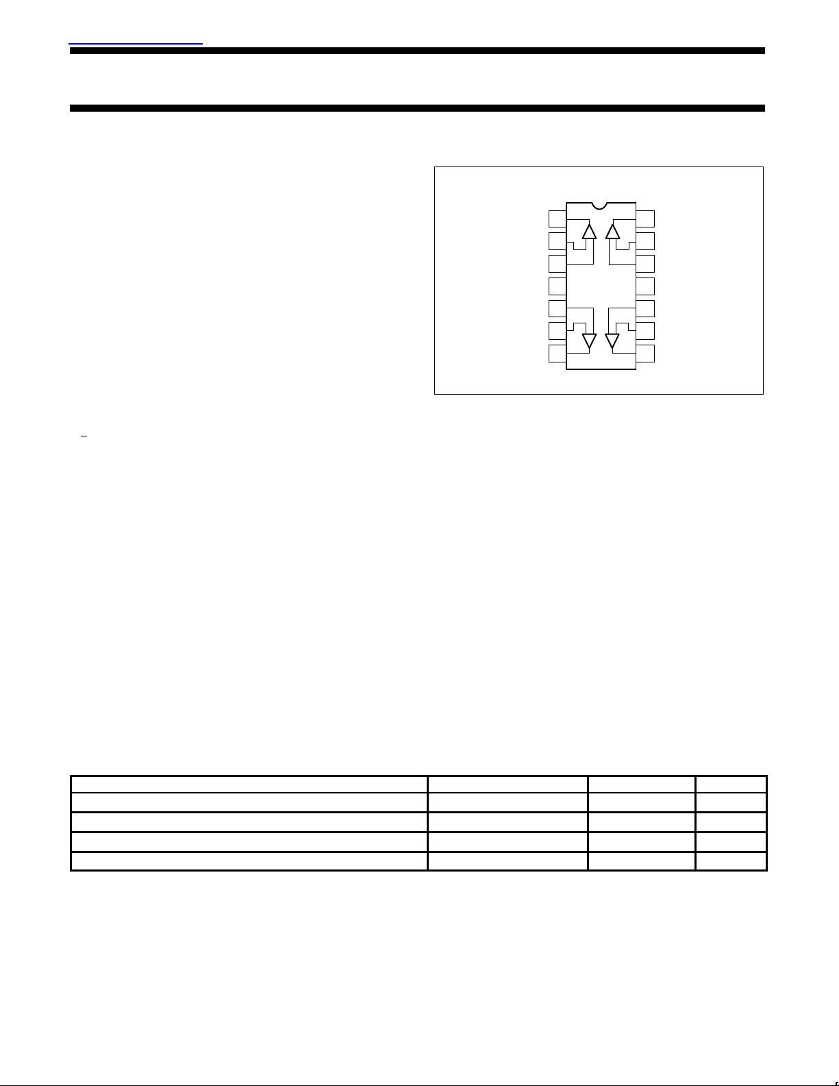
PIN CONFIGURATION
OUTPUT
1
1
-INPUT
1
2
+INPUT
1
3
V
CC
4
14 OUTPUT
4
13 -INPUT
4
12 +INPUT
4
11 GND
+INPUT
2
5
-INPUT
2
6
OUTPUT
2
7
10 +INPUT
3
9 -INPUT
3
8 OUTPUT
3
N, and D PACKAGES
TEMPERATURE RANGE ORDER CODE DWG #
14-Pin Plastic Small Outline (SO) package
0 to +70°C
NE5234D 0175D
14-Pin Plastic Dual In-Line Package (DIP)
0 to +70°C
NE5234N 0405B
14-Pin Plastic Small Outline (SO) package
-40 to +85°C
SA5234D 0175D
14-Pin Plastic Dual In-Line Package (DIP)
-40 to +85°C
SA5234N 0405B
查询NE5234供应商
APPLICATIONS
•Automotive electronics
•Signal conditioning and sensing amplification
•Portable instrumentation
– Test and measurement
– Medical monitors and diagnostics
– Remote meters
•Audio equipment
•Security systems
•Communications
– Pagers
– Cellular telephone
– LAN
– 5V Datacom bus
•Error amplifier in motor drives
•Transducer buffer amplifier
ORDERING INFORMATION
DESCRIPTION
Page 2
Philips Semiconductors Linear Products Product specification
NE/SA5234
Matched quad high-performance low-voltage
operational amplifier
August 31, 1994
160
ABSOLUTE MAXIMUM RATINGS
SYMBOL PARAMETER RATING UNITS
V
CC
Single supply voltage 7 V
V
ESD
ESD protection voltage at any pin
5
human body model
robot model
2000
200
V
V
V
S
Dual supply voltage +3.5 V
V
DP
Voltage at any device pin
1
VS + 0.5 V
I
DP
Current into any device pin
1
+ 50 mA
V
IN
Differential input voltage
2
0.5 V
V
CM
Common-mode input voltage (positive) VCC + 0.5 V
V
CM
Common-mode input voltage (negative) VEE - 0.5 V
P
D
Power dissipation
3
500 mW
T
J
Operating junction temperature
3
+150
°C
V
SC
Supply voltage allowing indefinite output short circuit to either rail
3,4
7 V
T
STG
Storage temperature range -65 to +150
°C
T
SOLD
Lead soldering temperature (10sec max) +300
°C
θ
JA
Thermal impedance
14 pin Plastic DIP 80
°C/W
14 pin Plastic SO 115
°C/W
NOTES:
1. Each pin is protected by ESD diodes. The voltage at any pin is limited by the ESD diodes.
2. The differential input of each amplifier is limited by two internal diodes, connected in parallel and opposite to each other . For more differential input range, use differential resistors in series with the input pins.
3. The maximum operating junction temperature is +150
°C. At elevated temperatures, devices must be derated according to the package
thermal resistance and device mounting conditions. Derates above +25
°C: F package at 6.7mW/°C; N package at 9.5mW/°C; D package
at 6.25mW/
°C.
4. Simultaneous short circuits of two or more amplifiers to the positive or negative rail can exceed the power dissipation ratings and cause
eventual destruction of the device.
5. Guaranteed by design.
RECOMMENDED OPERATING CONDITIONS
SYMBOL PARAMETER RATING UNITS
V
CC
Single supply voltage +2 to +5.5 V
V
S
Dual supply voltage +1 to +2.75 V
V
CM
Common-mode input voltage (positive) VCC + 0.25 V
V
CM
Common-mode input voltage (negative) VEE - 0.25 V
T
A
Temperature
NE 0 to +70
°C
SA -40 to +85
°C
Page 3
Philips Semiconductors Linear Products Product specification
NE/SA5234
Matched quad high-performance low-voltage
operational amplifier
August 31, 1994
161
DC ELECTRICAL CHARACTERISTICS
VCC = 2 to 5.5V, VEE = 0V, TA = 25°C; VEE < VCM < VCC; unless otherwise stated.
LIMITS
SYMBOL
PARAMETER
TEST CONDITIONS
NE5234 SA5234
UNITS
MIN TYP MAX MIN TYP MAX
VCC = 5.5V 2.8 4.0 2.8 4.0
VCC = 5.5V over full
temperature range
3.0 4.6 3.2 4.8
±0.2 ±4 ±0.2 ±4
Over full temperature
range
±0.4 ±5 ±0.6 ±5
∆VOS/∆T
Offset voltage drift with
temperature
4 4
µV/°C
0.4 3 0.4 3
∆V
OS
between any amplifiers in
the same package at the
same common mode level
1
Over full temperature
range
0.8 4 1.2 4
±3 ±20 ±3 ±30
Over full temperature
range
±4 ±30 ±6 ±60
∆IOS/∆T
Offset current drift with
temperature
0.02 ±.3 0.03 ±.3
nA/°C
VEE < VCM < V
EE
+0.5V
-200 -90 -200 -90
1
Over full temperature
range
-225 -100 -250 -150
IBInput bias current
1
VEE +1V < VCM < V
CC
25 70 25 75
nA
Over full temperature
range
35 100 35 120
∆IB/∆T
Input bias current drift with
temperature
0.5 0.5
nA/°C
VEE < VCM < V
EE
+0.5V
10 30 10 30
∆I
B
Over full temperature
range
25 50 50 70
same package at the same
common mode level.
VEE +1V < VCM < V
CC
5 20 5 20
nA
common mode level.
Over full temperature
range
15 30 25 50
VOS < 6mV VEE-0.25 VCC+0.25 VEE-0.25 VCC+0.25
VOS < 6mV over full
temperature range
VEE-0.1 VCC+0.1 VEE-0.1 VCC+0.1
VEE < VCM < VEE+0.5V,
V
EE
+1V < VCM < V
CC
100 90 100
ratio, small signal
Over full temperature
range
100 80 90
VEE < VCM < V
CC
90 100
Common-mode rejection
ratio, large signal
Over full temperature
range
80 90
VEE < VCM < V
CC
80 100 80 100
Over full temperature
range
80 90 80 90
I
V
Supply current
CC
Offset voltage
OS
Offset voltage difference
I
Offset current
OS
I
Input bias current
Input bias current difference
V
between any amplifier in the
Common-mode input range
CM
Common-mode rejection
CMRR
PSRR Power supply rejection ratio
mA
mV
mV
nA
nA
nA
V
dB
dB
Page 4
Philips Semiconductors Linear Products Product specification
NE/SA5234
Matched quad high-performance low-voltage
operational amplifier
August 31, 1994
162
DC ELECTRICAL CHARACTERISTICS (continued)
LIMITS
SYMBOL
PARAMETER
TEST CONDITIONS
NE5234 SA5234
UNITS
MIN TYP MAX MIN TYP MAX
10 12 10 12
Peak load current, sink and
source
Over full temperature
range
5 8 5 8
90 110 90 110
Over full temperature
range
90 90
I
PEAK
= 0.1mA
VEE+0.0
5
VCC-0.05 VEE+0.1 VCC-0.1
I
PEAK
= 10mA
VEE+0.2
5
VCC-0.25
VEE+0.2
5
VCC-0.25
I
PEAK
= 5mA over full
temp range
VEE+0.2
2
VCC-0.2 VEE+0.2 VCC-0.2
RL = 2kΩ VEE+0.2 VCC-0.2 VEE+0.2 VCC-0.2
Output voltage swing for
V
CC
= 2.75V, VEE = -2.75V
RL = 600Ω, VEE+0.2
5
VCC-0.25
VEE+0.2
5
VCC-0.25
NOTES:
1. These parameters are measured for V
EE
< VCM < VEE+.5V and for VEE+1V < VCM < VCC. By design these parameters are intermediate for
common mode ranges between the measured regions.
AC ELECTRICAL CHARACTERISTICS
TA = +25°C; VCC = 2 to 5.5V; RL = 10k; CL = 100pF; unless otherwise stated.
LIMITS
SYMBOL
PARAMETER
TEST CONDITIONS
NE5234 SA/SE5234
UNITS
MIN TYP MAX MIN TYP MAX
SR Slew rate
Over full temperature
range
0.5 0.8 0.5 0.8 V/µs
BW Unity gain bandwidth: -3dB
Over full temperature
range
2 2.5 4.0 2 2.5 4.0 MHz
θ
M
Phase Margin CL = 50pF 55 55 deg
t
S
1% settling time AV = 1, 1V step 1.4 1.4 µs
V
N
Input referred voltage noise
AV = 1, RS = 0Ω, at
1kHz
25 25
nV/Hz
1/2
THD Total harmonic distortion 10kHz, 1V
P-P
, AV = 1 0.1 0.1 %
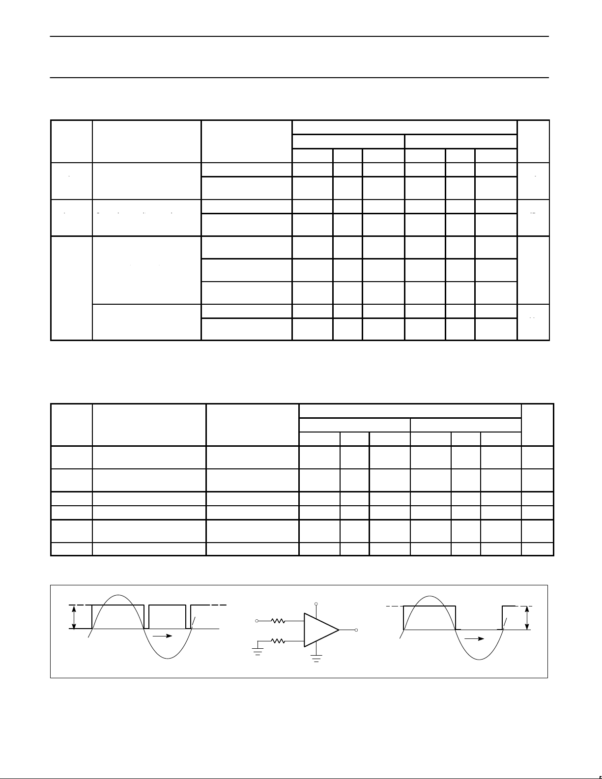
OUTPUT INVERSION PREVENTION
47k
47k
V
IN
V
OUT
V
CC
+
–
5V
CONVENTIONAL OP AMP PHILIPS NE5234
t
t
V
CC
V
OUT
V
OUT
V
IN
V
IN
V
GND
V
GND
V
GND
V
CC
5V
I
A
V
L
Open-loop voltage gain
VOL
Output voltage swing
OUT
mA
dB
V
V
 Loading...