

Page 1
FRONTEND 4049 FM5 3x8168; 3x8292
TARGET SPECIFICATION ELECTRICAL DATA
1. Description:
The frontend 4049 FM5 is specially designed for multimedia applications. It includes TV as well as
FM reception possibility. TV reception standard are B/G; I, D/K, L, L`. The frontend includes a
hyperband tuner which covers the frequency range from 45 to 865 MHz and an IF-part with SAWfilter, IF-amplifier, video- and sound demodulator. So the AF signal is available at the audio output
terminal, the CVBS signal is available at the video output terminal. Also a 2
which allows external sound demodulation for stereo and NICAM reception. A video buffer is built
in which makes a direct connection to 75 Ω inputs possible. The reception frequency range is
divided in VHF low, VHF high and UHF.
VHFlow part of the tuner is used for FM reception also. Complete FM signal processing including
demodulation and stereo decoding is built in. Baseband signals L (left) and R (right) as well as
MPX (Baseband Multiplex signal) are on pins available.
Band, standard selection and tuning are done via I²C-bus, completely. Also a digital AFC-function
can be realized, because the AFC-voltage generated by the IF-demodulator is fed to an
analogue/digital converter which is integrated in the IF demodulator-IC and readable via I²C-bus.
A DC/DC converter is built in. Therefore supply voltage is 5V only.
2. Mechanical Characteristics:
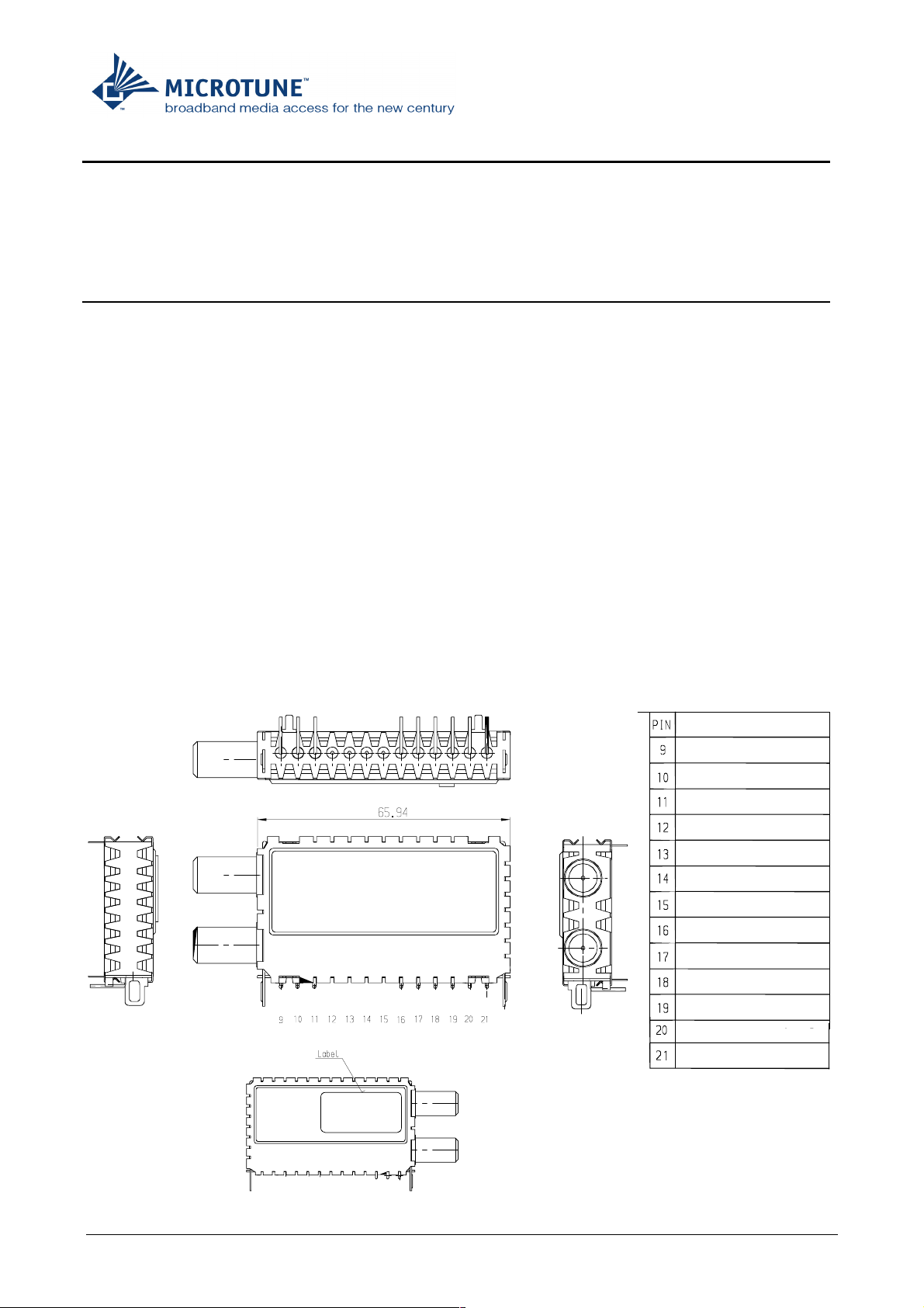
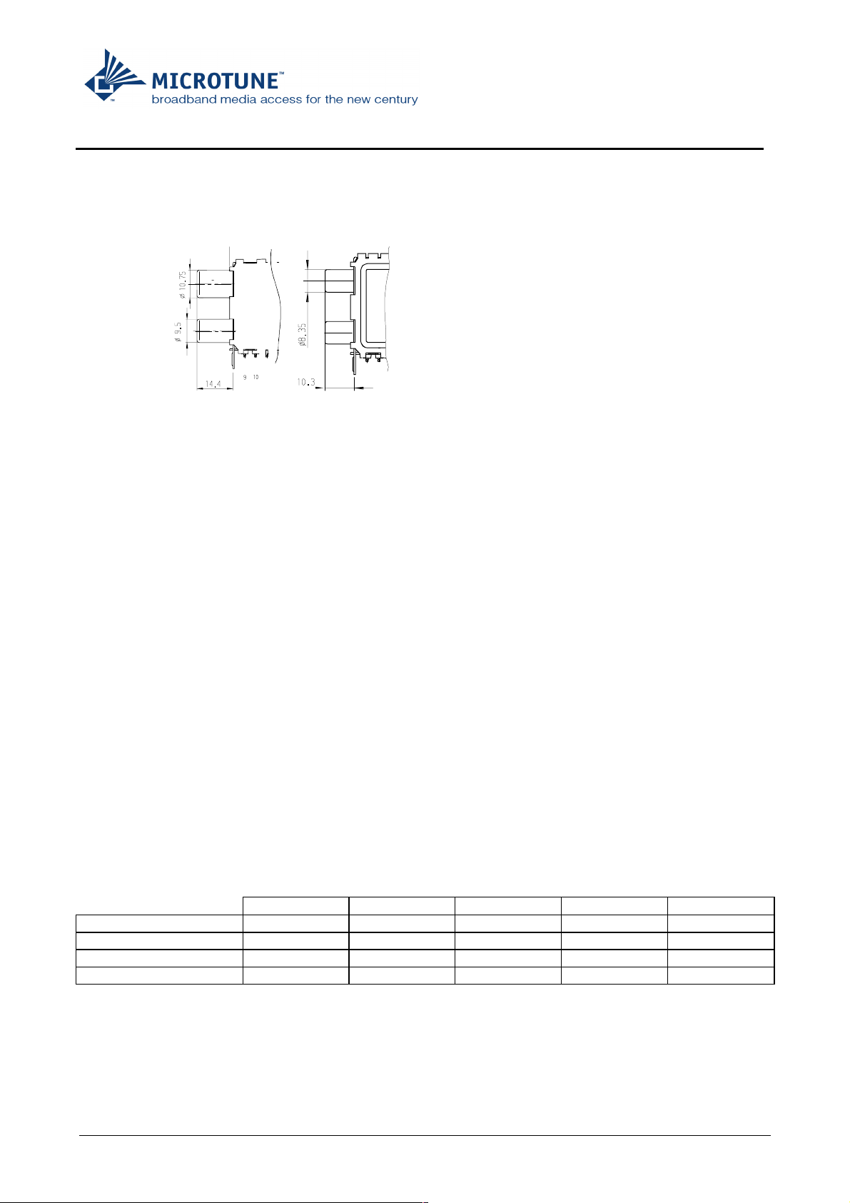
2.1. Dimensions: according drawing 3x8168GZ
2.2. Weight: appr. 52 g
nd
IF output is provided,
I²C bus signal SCL
I²C bus signal SDA
Address selection for I²C bus
FM sound output R
FM sound output L
2nd IF
Video output CVBS
Supply voltage V
AF sound output / FM MPX
S1
3X8168 ED Page: 1/14
November 02
8168ED01.DOC
Page 2
2.3. Types
Tunertype 3x8168 3x8292
Sockettype IEC connectors Phono sockets
Socketlength 14.4 mm 10.3 mm
Height 28.55/10.25 mm 28.55/10.25 mm
3. Working Data:
3.1. Reception Standard: B/G, I, D/K, L, L`
3. 2. Frequency Range:
VHF low ch IA ...S6 45.75 MHz ... 140.25 MHz
VHF high ch S7 ...S41 147.25 MHz ... 463.25 MHz
UHF ch 21 ...69 471.25 MHz ... 855.25 MHz
FM 87.50 MHz … 108.10 MHz
Margin:
VHF low ch IA ... S6 +0.5 MHz/-0.25 MHz
VHF high ch S7... S41 +1 MHz/-6 MHz
UHF ch 21 ... 69 +3 MHz/-6 MHz
FM +/- 0.5 MHz
Recommened take over frequencies:
VHF low / VHF high 141 MHz
VHF high/ UHF 464 MHz
Frequency referred to picture carrier.
IF:
B, G I L L` D/K
picture carrier 38.9 38.9 38.9 33.90 38.9
sound carrier 1 33.4 32.9 32.4 40.40 32.4
sound carrier 2 33.16
NICAM sound carrier 33.05 32.348 33.05 33.05
all frequencies in MHz
Oscillator operates above received frequency.
3X8168 ED Page: 2/14
November 02
8168ED01.DOC
Page 3

3.3. Supply voltage:
Supply voltage VS1 5 V +/- 5% max. 230 mA
3.4. Input impedance:
VHF/UHF and FM 75 Ω, unbalanced
3.5. Temperature:
Operating temperature: 0 ... 60 °C
Storage temperature: -25 ... 60 °C
( measured in slowly moved air )
4. Test conditions:
If not otherwise noticed all data are hold under following conditions:
Measurement tolerance: 10 % or 1 dB
Ambient temperature: 25 °C +/- 3°
Supply voltage: V S1 +/- 5%
5. TV Tuner Data:
5.1. VSWR: min. typ. max. unit
VHF low 5.0
VHF high 5.0
UHF 5.0
Referred to channel center frequency.
5.2. AGC-Range:
VHF low 40 dB
VHF high 40 dB
UHF 35 dB
FM 40 dB
5.3. IF-Rejection:
VHF low 50 dB
VHF high 60 dB
UHF 60 dB
FM 50 dB
5.4. Image-Rejection:
VHF low 60 dB
VHF high ch S7 .... ch S20 60 dB
VHF high ch S21 .... ch S41 55 dB
UHF 50 dB
FM 50 dB
3X8168 ED Page: 3/14
November 02
8168ED01.DOC
Page 4

6. TV Output parameter:
6.1. Video output:
Conditions:
CVBS - Output level (B/G, D/K, L/L`): 1 V
(Standard I): 0.9 V
Load impedance 75 Ω
Video S/N (unweighted):
VHF 46 dB
UHF 47 dB
Video sensitivity (Off Air Channels) 45 dBµV
Video S/N = 30 dB
Frequency response:
(sin x)/x Ref.: 0.2 MHz
2 MHz -2 3 dB
3 MHz -4 3 dB
4 MHz -4 4 dB
4.43 MHz -5 3 dB
5 MHz -12 dB
sound carrier rejection
B/G 30 dB
I, D/K, L/L´ 26 dB
Differential gain
Differential phase
1 MHz -1.5 2 dB
min. typ. max. unit
Standard B/G; Ant. input level 66 dBµV
Flat Field
modulated 5 step staircase
modulated 5 step staircase
3 %
5 °pp
pp
pp
pp
3X8168 ED Page: 4/14
November 02
8168ED01.DOC
Page 5

: 20dB)
rms
rms
pp
pp
pp
6.2 TV Sound output:
Pin 21 min. typ. max. unit
Load DC 100 kΩ
AC 10 kΩ
Output level: DC 2.3 V
6.2.1 TV FM sound
Conditions:
Ant.input level 66 dBµV; Video signal: color bar
Audio signal 1kHz, 27 kHz deviation; 50 µs preemphasis
Measurements with 50 µs deemphasis:
AF - level: 400 540 680 mV
THD: 0.5 %
S/N: 50 dB
Frequency response: 40 Hz ... 15 kHz -1 1 dB
(6 kHz deviation)
6.2.2 TV AM sound
input level 66 dBµV, video signal: color bar
audio signal 1kHz AM 54% modulation
AF - level: 400 500 600 mV
THD: 1.0 %
S/N: 45 dB
6.3. 2nd IF output
AC level of SC
(PC/ sound carrier SC1: 7, 10, 13 dB)
(sound carrier SC
AC level of SC1 6.5 MHz: 400 mV
(PC/ sound carrier: 10 dB)
(L standard, without modulation)
AC level of SC2 5.74, 6.55 MHz: 125 mV
(PC/ sound carrier SC1: 10 dB)
(PC/ sound carrier SC
Load impedance 0.5 kΩ
5.5, 6.0, 6.5 MHz: 400 mV
1
off )
2
2
3X8168 ED Page: 5/14
November 02
8168ED01.DOC
Page 6

7. FM part
7.1 FM output
min. typ. max. unit
7.1.1 Frequency range 87.5 108.1 MHz
7.1.2 Output levels
MPX AC 810 mVrms
DC 2.3 V
Load impedance 100 kΩ
L, R resp. AC 255 mVrms
DC 1.0 V
Load impedance 100 kΩ
7.1.3 Frequency response
40 Hz to 15 kHz -2 2 dB
7.1.4 Usable sensivity
30 dB S/N 5 dBµV
50 dB S/N 15 dBµV
7.1.5 S/N at high input level 65 dB
75 kHz deviation
measured at MPX output with 50 µs deemphasis
7.1.6 Distortion at high input level 0.2 %
22.5 kHz deviation
7.1.7 Stereo channel separation 30 dB
7.1.8 AM suppression 60 dB
7.1.9 Image rejection 53 80 dB
7.1.10 IF rejection 50 dB
AF = 1 kHz, 75 kHz deviation
1 kHz 75 kHz deviation
Vin = 60 dBµV, Mod. = 1kHz
Vin 60 dBµV 75 kHz dev. AM 30%
unwanted signal 66.6 MHz above wanted signal
referred to 33.3 MHz unwanted signal
3X8168 ED Page: 6/14
November 02
8168ED01.DOC
Page 7
8. I²C bus
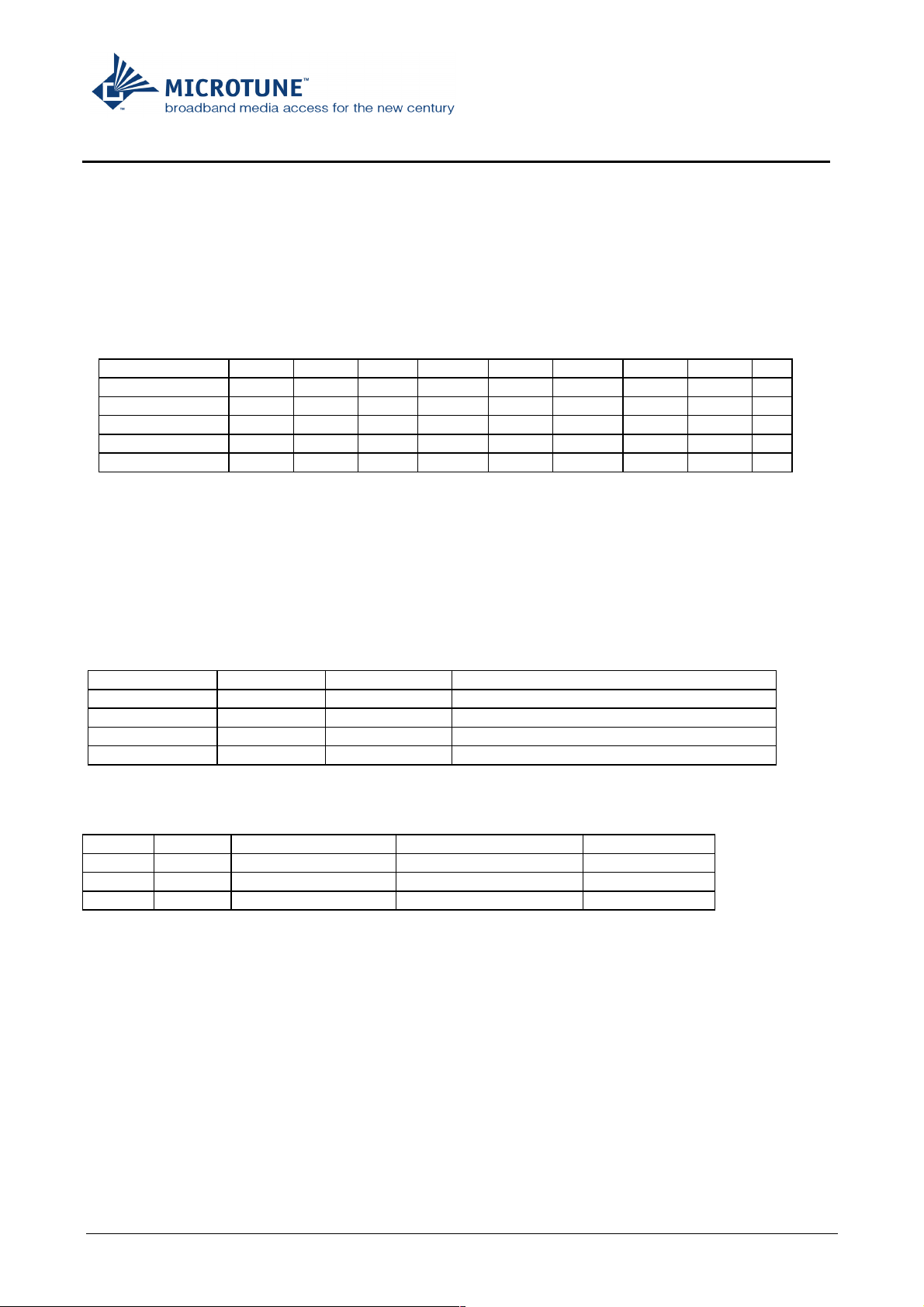
There are two different I²C bus used one I²C Tuner to control tuning and one I²C IF to control IF
demodulation and baseband processing. With port P0 of control byte 2 the slave address of I
controlled.
8.1 I²C Tuner
8.1.1 Write data format
MSB LSB
Address byte 1 1 0 0 0 MA1 MA0 R/W A
Divider byte 1 0 n14 n13 n12 n11 n10 n9 n8 A
Divider byte 2 n7 n6 n5 n4 n3 n2 n1 n0 A
Control byte 1 1 CP T2 T1 T0 RSA RSB OS A
Control byte 2 P7 P6 P5 P4 P3 P2 P1 P0 A
2
C IF can be
A = Acknowledge
R/W = 0 : Write mode
CP = 1 : charge pump current high
T2, T1, T0 = test bits, normal operation: T2 = 0, T1 = 0, T0 = 1
RSA, RSB bits for minimum step size, see 8.1.2
OS = tuning voltage switch, normal operation: OS = 0
8.1.2 Address selection
MA1 MA0 Address Voltage at Pin 11
0 0 C0 ( 0 to 0.1 ) * VS1
0 1 C2 (0.2 to 0.3) * VS1 or open
1 0 C4 ( 0.4 to 0.6 ) * VS1
1 1 C6 ( 0.9 to 1 ) * VS1
8.1.3 Oscillator frequency and divider byte calculation:
RSA RSB Reference divider Min. tuning step [kHz] f
1 1 512 62.5 7.8125
X 0 640 50.0 6.25
0 1 1024 31.25 3.90625
for FM recption we recommend 50 kHz minimum step size
= fD + fIF
f
OSC
f
f
f
= 38.9 MHz at B/G, D/K, I, L
IF
= 33.9 MHz at L’
IF
= 33.3 MHz at FM
IF
: Local oscillator frequency
f
OSC
: Desired frequency
f
D
f
= f
* 8 * SF
REF
: Crystal reference frequency / 640 = 4 MHz / 640 = 6.25 kHz, ( RSA =X, RSB = 0)
f
OSC
REF
SF : Programmable scaling factor
[kHz]
ref
Scaling factor
SF= 16384* n14 + 8192 * n13 * 4096 * n12 + 2048 * n11 + 1024 * n10 + 512 * n9 + 256* n8 + 128 * n7 +
64 * n6 + 32 * n5 + 16 * n4 + 8 * n3 + 4 * n2 + 2 * n1 + n0
3X8168 ED Page: 7/14
November 02
8168ED01.DOC
Page 8
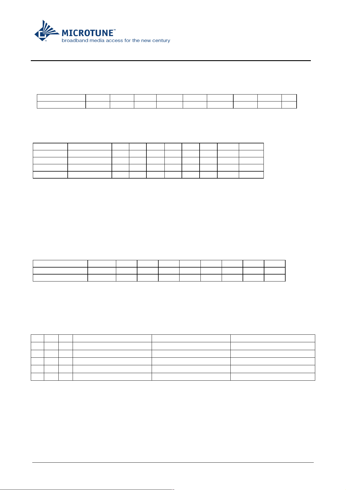
8.1.4 Control byte 1 settings (default)
MSB LSB
Control byte 1 1 0 0 0 1 X 0 0 A
8.1.5 Control byte 2 (Bandselection)
Band Active port P7 P6 P5 P4 P3 P2 P1 P0
VHF low P7, P5 1 0 1 0 0 0 0 MAD
VHF high P7,P4 1 0 0 1 0 0 0 MAD
UHF P5,P4 0 0 1 1 0 0 0 MAD
FM P7, P5, P2 1 0 1 0 0 1 MS MAD
MAD: Programmable module address I
0 = Slave address I
1 = Slave address I
2
C IF = 43[hex]
2
C IF = 42[hex]
MS: Forced Mono at FM mode:
0 = Stereo Mode with capability of stereo indication
1 = Forced Mono Mode
8.1.6 Read data format
MSB LSB
Address byte 1 1 0 0 0 MA1 MA0 R/W A
Status byte POR FL I2 I1 I0 A2 A1 A0 A
R/W : 1 = Read mode
POR : Power on reset flag ( POR =1 at power on)
FL : In lock flag (FL= 1 when PLL is locked)
I2, I1, I0: Digital levels for I/O ports P2, P1 and P0 respect.
In case of FM I1 = 1: Stereo indication
I2, I0 not defined
A2, A1, A0: FM-AFC or FM-AGC or SIF-AGC radio output detection
A2 A1 A0 SIF-AGC radio output *1) FM-AGC radio output *2) FM-AFC radio output *3)
1 0 0 not defined not defined -100 kHz
0 1 1 > 20dBµV normal signal -35 kHz
0 1 0 5dBµV … 20dBµV weak signal Correct tuning
0 0 1 <5dBµV very weak signal +35 kHz
0 0 0 not defined not defined +100 kHz
*1) typical values, peak level detection within a bandwith of appr. 2MHz
*2) only valid if FM-carrier exist and SIF-AGC radio output = (A2=0, A1=1, A0=1)
*3) typical values, only valid if CARRDET = high, see section 8.3.2
2
C IF
3X8168 ED Page: 8/14
November 02
8168ED01.DOC
Page 9
8.2. I²C IF
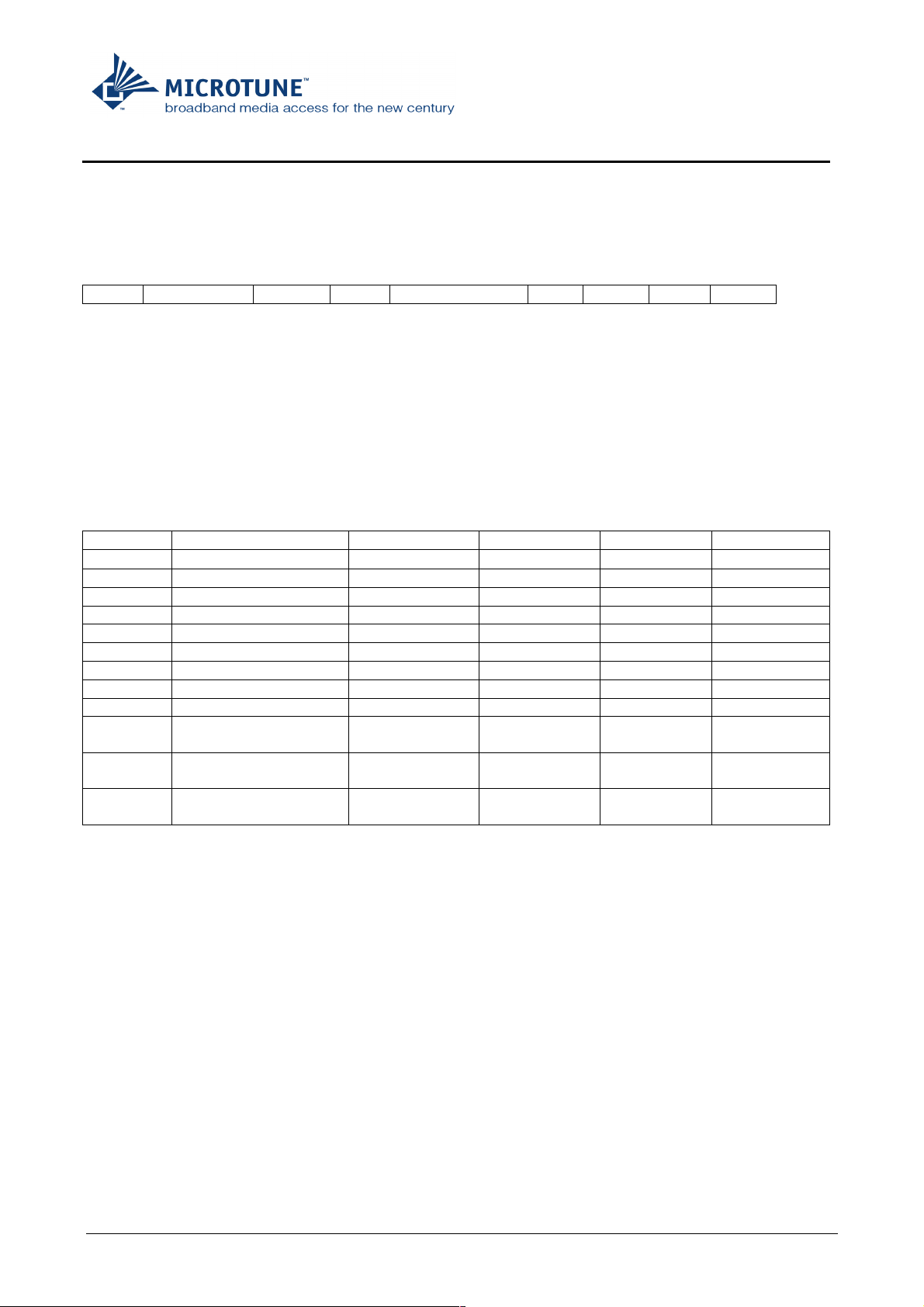
8.2.1. I²C-bus sequence write
Start Slave addr. R/W =0 Ack subaddress Ack data Ack Stop
Start start condition.
Slave addr Slave address (7bit) = 42[hex] or 43[hex] in respect of MAD.
R/W Read/Write bit: 0 = write to component; 1 = master reads from component.
Subaddress byte which indicates register of component which the are data for.
“switching register” 00[hex]
“adjust register” 01[hex]
“data register” 02[hex]
Ack acknowledge generated by the component
Stop stop condition
If more than one byte of data is transmitted, then auto-increment of subaddress is performed.
i.e. transmit 3 bytes starting with data for switch register
mode Slave addr + R/W =0 Subaddress switch reg. adjust reg. data reg.
MAD=0 / MAD=1
B/G 86 / 84 00 D4 70 09
I 86 / 84 00 D4 70 0A
D/K 86 / 84 00 D4 70 0B
L 86 / 84 00 C4 10 0B
L` 86 / 84 00 84 10 13
FM - AFC 86 / 84 00 DC 70 1D
FM - AGC 86 / 84 00 DC 70 9D
SIF - AGC 86 / 84 00 DC 70 81
FM - AFC
86 / 84 00 DC 10 1D
stereo
FM - AGC
86 / 84 00 DC 10 9D
stereo
SIF – AGC
86 / 84 00 DC 10 81
stereo
all bytes in [hex]
3X8168 ED Page: 9/14
November 02
8168ED01.DOC
Page 10
8.2.2 switch register
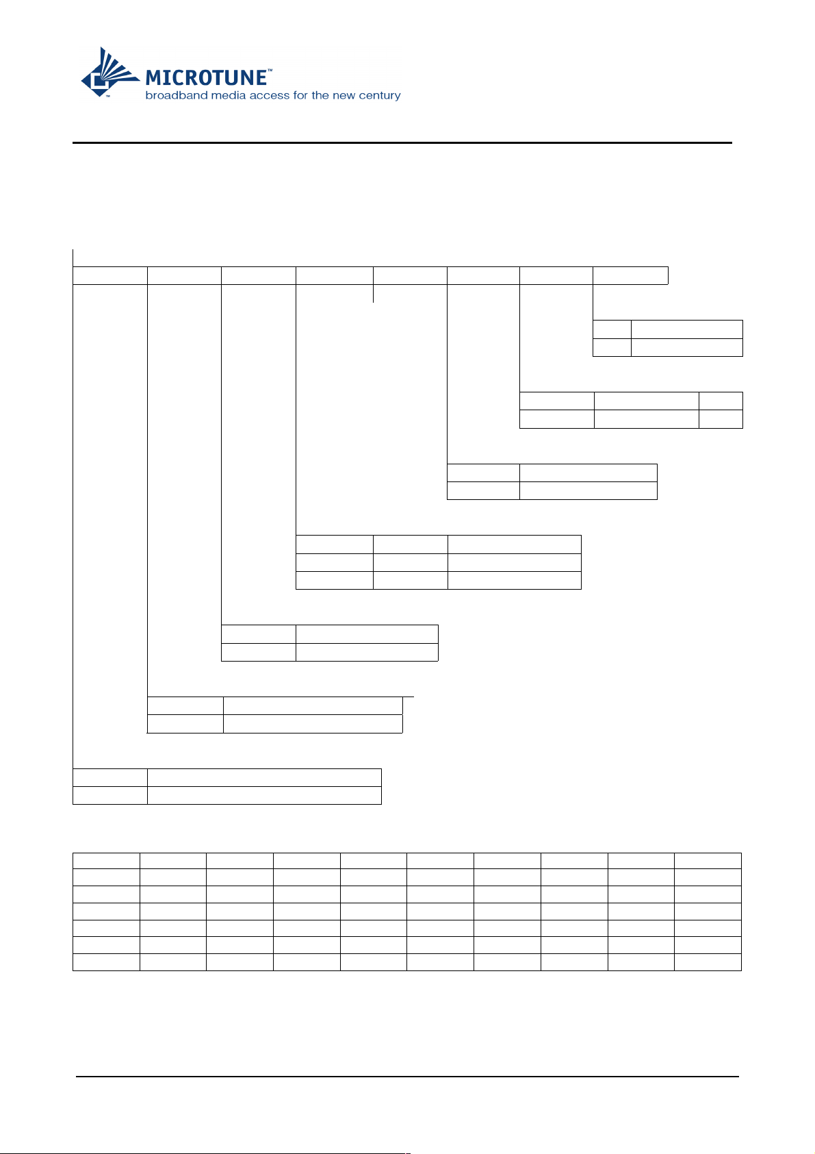
acc. Chapter 8.2.1 switch register is addressed by subaddress 00 [hex]
switch register
B7 B6 B5 B4 B3 B2 B1 B0
Video mode
0
1
Audio mute FM
0 Inactive
1 active
Carrier mode
0 intercarrier
1 QSS
Modulation
0 0 Positive AM TV
1 0 Negative TV
x 1 FM Radio
Forced mute audio
0 off
1 on
Output port 1 (Audio-SAW switch)
0 L’
1 B/G, D/K, I, L
Output port 2 (not used)
0 Low ohmic active
1 High ohmic disabled
Recommended settings switch register
mode
B/G
I
D/K
L
L`
FM
B7 B6 B5 B4 B3 B2 B1 B0 =[hex]
1 1 0 1 0 1 0 0
1 1 0 1 0 1 0 0
1 1 0 1 0 1 0 0
1 1 0 0 0 1 0 0
1 0 0 0 0 1 0 0
1 1 0 1 1 1 0 0
Sound bypass off
Sound bypass on
D4
D4
D4
C4
84
DC
3X8168 ED Page:
10/14
November 02
8168ED01.DOC
Page 11
8.2.3 Adjust register
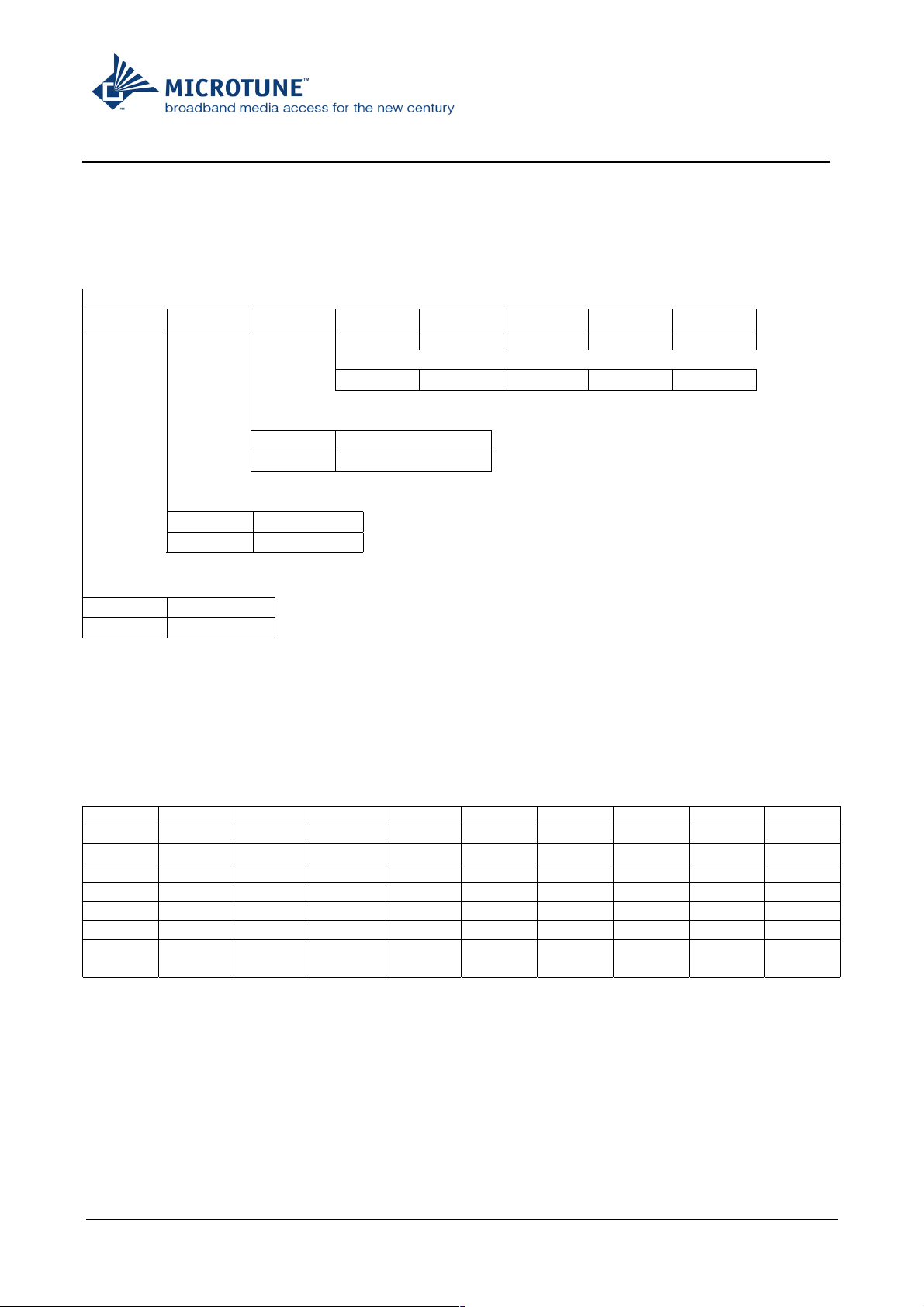
acc. Chapter 8.2.1 adjust register is addressed by subaddress 01 [hex]
Adjust register
C7 C6 C5 C4 C3 C2 C1 C0
AGC adjustment
1 0 0 0 0
Deemphasis
0 De-emphasis off
1 De-emphasis on
Value of de-emphasis
0 75 us
1 50 us
Audio gain
0 0 dB
1 -6 dB
Recommended settings adjust register
mode
B/G
I
D/K
L
L`
FM
FM
stereo
C7 C6 C5 C4 C3 C2 C1 C0 =[hex]
0 1 1 1 0 0 0 0
0 1 1 1 0 0 0 0
0 1 1 1 0 0 0 0
0 0 0 1 0 0 0 0
0 0 0 1 0 0 0 0
0 1 1 1 0 0 0 0
0 0 0 1 0 0 0 0
70
70
70
10
10
70
10
3X8168 ED Page:
11/14
November 02
8168ED01.DOC
Page 12
8.2.3 data register
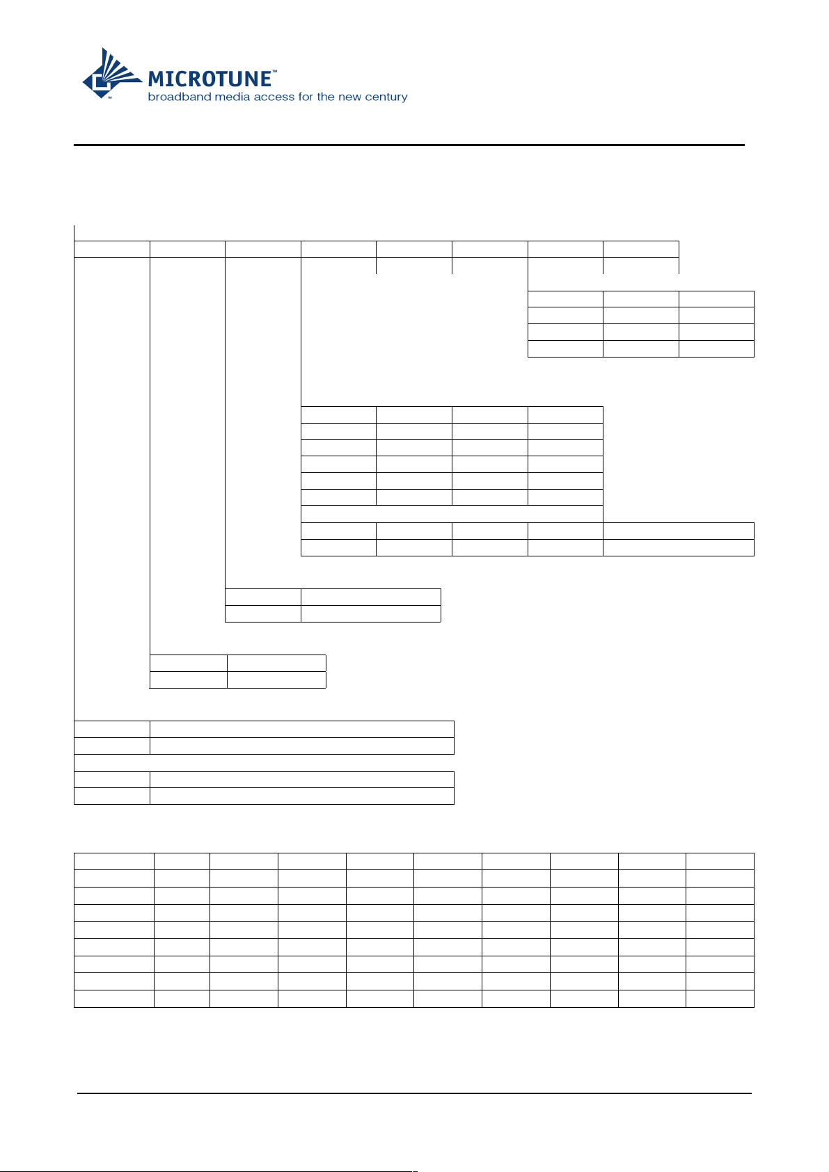
acc. Chapter 8.2.1 data register is addressed by subaddress 02 [hex]
data register
E7 E6 E5 E4 E3 E2 E1 E0
0 0 4.5
0 1 5.5
1 0 6.0
1 1 6.5
Video IF
TV Mode: B3=0
0 0 0 58.75
0 0 1 45.75
0 1 0 38.9
0 1 1 38.0
1 0 0 33.9
1 0 1 33.4
Radio Mode: B3=1
0 0 0 44 SIF-AGC radio output
1 1 1 44 FM-AGC radio output
VIF, SIF, tuner gain
0 Normal gain
1 Minimum gain
Gating (pos. AM)
0 0 %
1 36 %
VIF AGC output – TV Mode: B3=0
0 Normal port function (Output port2)
1 No port function
PIN 21 output – Radio Mode: B3=1
0 FM-AFC radio output
1 FM-AGC or SIF-AGC radio output acc. E2…E4
Recommended settings data register
mode
B/G
I
D/K
L
L`
FM-AFC
FM-AGC
SIF-AGC
E7 E6 E5 E4 E3 E2 E1 E0 =[hex]
0 0 0 0 1 0 0 1
0 0 0 0 1 0 1 0
0 0 0 0 1 0 1 1
0 0 0 0 1 0 1 1
0 0 0 1 0 0 1 1
0 0 0 1 1 1 0 1
1 0 0 1 1 1 0 1
1 0 0 0 0 0 0 1
nd
2
IF
MHz
MHz
09
0A
0B
0B
13
1D
9D
81
3X8168 ED Page:
12/14
November 02
8168ED01.DOC
Page 13
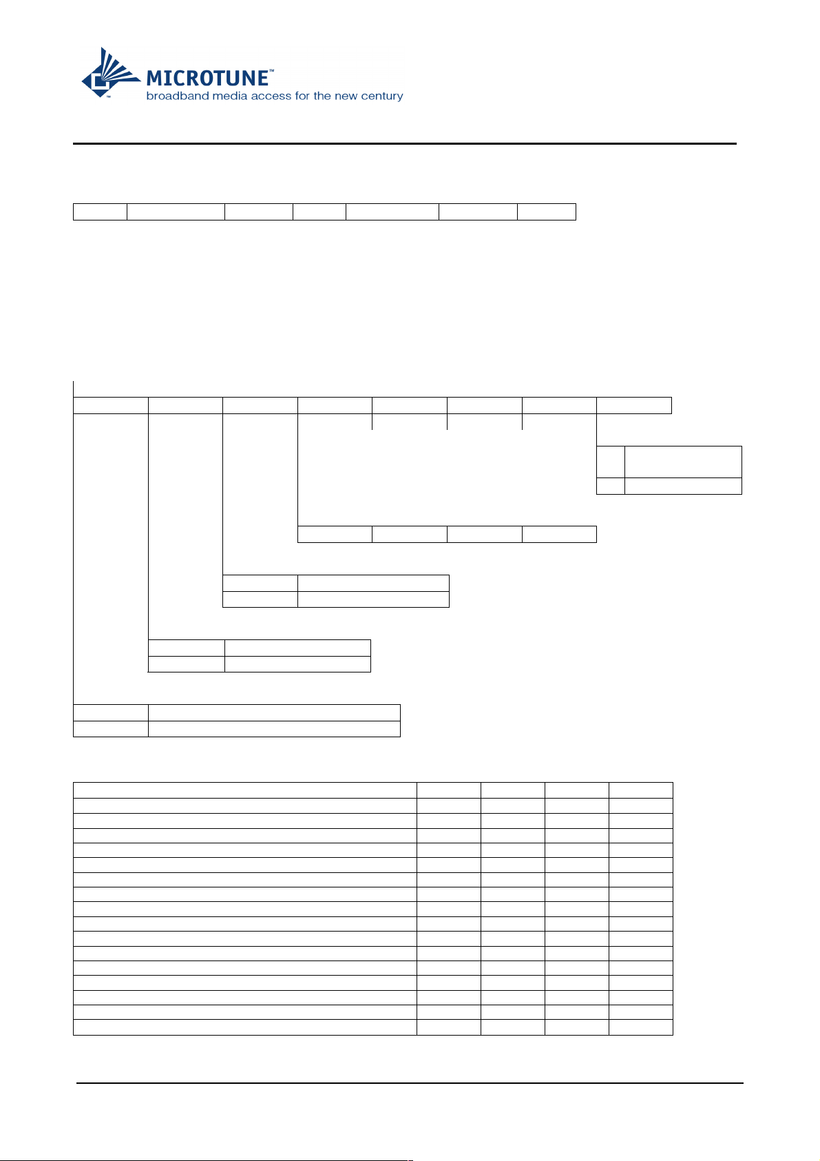
8.3.1. I²C-bus sequence read
Start Slave addr. R/W =1 Ack data Ack not Stop
Start start condition.
Slave addr Slave address = 43[hex].
R/W Read/Write bit: 0 = write to component; 1 = master reads from component.
Ack acknowledge, generated by the component
Ack not acknowledge, generated by the master
Stop stop condition
8.3.2 Read data format
Status register
Bit7 Bit6 Bit5 Bit4 Bit3 Bit2 Bit1 Bit0
Power on reset
0 Normal
operation
1 Power on reset
AFC value
AFC4 AFC3 AFC2 AFC1
CARRDET – FM carrier detection
0 FM carrier not detected
1 FM carrier detected
VIFLEV - VIF level input
0 VIF low level
1 VIF high level
AFCWIN - AFC window (Note 1)
0 Tuning out of window (+/- 1.6 MHz)
1 Tuning in window (+/- 1.6 MHz)
Note1. If no IF input is applied, then bit AFCWIN = 1 due to the fact that the VCO is forced to the AFC window border for
fast load-in behaviour.
Automatic Frequency Control f
f
≤ f0 – 187.5 kHz
VIF
f
= f0 – 162.5 kHz 0 1 1 0
VIF
f
= f0 – 137.5 kHz 0 1 0 1
VIF
f
= f0 – 112.5 kHz 0 1 0 0
VIF
f
= f0 – 87.5 kHz 0 0 1 1
VIF
f
= f0 – 62.5 kHz 0 0 1 0
VIF
f
= f0 – 37.5 kHz 0 0 0 1
VIF
f
= f0 – 12.5 kHz 0 0 0 0
VIF
f
= f0 + 12.5 kHz 1 1 1 1
VIF
f
= f0 + 37.5 kHz 1 1 1 0
VIF
f
= f0 + 62.5 kHz 1 1 0 1
VIF
f
= f0 + 87.5 kHz 1 1 0 0
VIF
f
= f0 + 112.5 kHz 1 0 1 1
VIF
f
= f0 + 137.5 kHz 1 0 1 0
VIF
f
= f0 + 162.5 kHz 1 0 0 1
VIF
f
≥ f0 + 187.5 kHz
VIF
Versus f0 AFC4 AFC3 AFC2 AFC1
VIF
0 1 1 1
1 0 0 0
3X8168 ED Page:
13/14
November 02
8168ED01.DOC
Page 14
9. ESD Protection
The frontend contains components that can be damaged by static discharge.
Observe these precautions: Ground yourself before handling the frontend.
Do not touch the frontend connector pins without ESD protection.
NAME J. Kreil
DATE 07.November 2002
REV.: 01
FÄM.- NO.
DATE 07.11.2002
NAME J. Kreil
SIGNATURE
3X8168 ED Page:
14/14
November 02
8168ED01.DOC
 Loading...