

Philips MDV-430-VT Service manual
MANUAL 5881 Digital Video Disc Player & Video Cassette Recorder MAGNAVOX MDV530VR/17
Philips Consumer Electronics Company
A Division of Philips Electronics North America Corporation
Technical Service Data
Service So luti on s Grou p
Technical Publications Dept.
P.O. Box 555, 401 E. Old Andrew Johnson Hwy.
Jefferson City,TN 37760
Sec. 1A: Main Section
( MDV530VR/17 )
Specifications
Operating Instructions
Adjustment Procedures
Schematic Diagrams and CBA’s
Exploded Views
Cabinet & Electrical Parts Lists
Sec. 2: Deck Mechanism Secti o n
Digital Video Disc Player &
Video Cassette Recorder
MANUAL 5888
Service Manual
MAGNAVOX
Model: MDV530VR/17
Digital Video Disc Player & Video Cassette Recor der
First Issue: 3/03
2003 Philips Consumer Electronics Company
Philips Consumer Electronics Company
A Division of Philips Electronics North America Corporation
MANUAL 5888
Technical Service Data
Service So luti on s Grou p
Technical Publications Dept.
P.O. Box 555, 401 E. Old Andrew Johnson Hwy.
Jefferson City,TN 37760
Sec. 1A: Main Section
( MDV530VR/17 )
Specifications
Operating Instructions
Adjustment Procedures
Schematic Diagrams and CBA’s
Exploded Views
Cabinet & Electrical Parts Lists
Digital Video Disc Player &
Video Cassette Recorder
Service Manual
MAGNAVOX
Model: MDV530VR/17
Digital Video Disc Player & Video Cassette Recor der
First Issue: 3/03
2003 Philips Consumer Electronics Company

IMPORTANT SAFETY NOTICE
Proper service and repair is important to the safe, reliable operation of all
Philips Consumer Electronics Com pany** Equipment. The service pr ocedures
recommended by Philips and described in this service manual are effective
methods of performing service operations. Some of these service operations
require the use of tools specially designed for the purpose. The special tools
should be used when and as recommended.
It is important to note that this manual contains various CAUTIONS and
NOTICES which should be carefully read in order to minimize the risk of personal injury to service personnel. The possibility exists that improper service
methods may damage the equipment. It also is important to understand that
these CAUTIONS and NOTICES ARE NOT EXHAUSTIVE. Philips could not
possibly know, evaluate and advise the service trade of all conceivable ways
in which service might be done or of the possible hazardous consequences of
each way. Consequently, Philips has not undertaken any such broad evaluation. Accordingly, a servicer who uses a service procedure or tool which is
not recommended by Philips must first satisfy himself thoroughly that neither
his safety nor the safe operation of the equipment will be jeopardized by the
service method selected.
** Hereafter throughout this manual, Philips Consumer Electronics Company
will be referred to as Philips.
WARNING
Critical components having special safety characteristics are identified
with a # by the Ref. No. in the parts list and enclosed within a broken
line* (where several critical components are grouped in one area) along
with the safety symbol # on the schematics or exploded views.
Use of substitute replacement parts which do not have the same specifie d
safety characteristics may create shock, fire, or other hazards.
Under no circumstances should the original design be modified or altered
without written permission from Philips. Philips assumes no liability,
express or implied, arising out of any unauthorized modification of
design. Servicer assumes all liability.
* Broken Line
Manufactured under license from Dolby Laboratories. "Dolby"
and the double-D symbol are trademarks of Dolby Laboratories.

TABLE OF CONTENTS
[ Main Section ]
Page
SPECIFICATIONS . . . . . . . . . . . . . . . . . . . . . . . . . . . . . . . . . . . . . . . . . . . . . . . . . . . . . . . . . . . . . . . . . . . . . . . 1-1-1
LASER BEAM SAFETY PRECAUTIONS. . . . . . . . . . . . . . . . . . . . . . . . . . . . . . . . . . . . . . . . . . . . . . . . . . . . . . 1-2-1
IMPORTANT SAFETY PRECAUTIONS. . . . . . . . . . . . . . . . . . . . . . . . . . . . . . . . . . . . . . . . . . . . . . . . . . . . . . . 1-3-1
STANDARD NOTES FOR SERVICING . . . . . . . . . . . . . . . . . . . . . . . . . . . . . . . . . . . . . . . . . . . . . . . . . . . . . . . 1-4-1
PREPARATION FOR SERVICING . . . . . . . . . . . . . . . . . . . . . . . . . . . . . . . . . . . . . . . . . . . . . . . . . . . . . . . . . . . 1-5-1
OPERATING CONTROLS AND FUNCTIONS. . . . . . . . . . . . . . . . . . . . . . . . . . . . . . . . . . . . . . . . . . . . . . . . . . 1-6-1
REMOTE CONTROL OPERATION . . . . . . . . . . . . . . . . . . . . . . . . . . . . . . . . . . . . . . . . . . . . . . . . . . . . . . . . . . 1-7-1
CABINET DISASSEMBLY INSTRUCTIONS . . . . . . . . . . . . . . . . . . . . . . . . . . . . . . . . . . . . . . . . . . . . . . . . . . . 1-8-1
ELECTRICAL ADJUSTMENT INSTRUCTIONS . . . . . . . . . . . . . . . . . . . . . . . . . . . . . . . . . . . . . . . . . . . . . . . . 1-9-1
Adjustment Points and Test Points . . . . . . . . . . . . . . . . . . . . . . . . . . . . . . . . . . . . . . . . . . . . . . . . . . . . . . . . 1-9-2
FIRMWARE RENEWAL MODE . . . . . . . . . . . . . . . . . . . . . . . . . . . . . . . . . . . . . . . . . . . . . . . . . . . . . . . . . . . . . 1-10-1
BLOCK DIAGRAM
Servo/System Control Block Diagarm. . . . . . . . . . . . . . . . . . . . . . . . . . . . . . . . . . . . . . . . . . . . . . . . . . . . . . 1-11-1
Video Block Diagarm. . . . . . . . . . . . . . . . . . . . . . . . . . . . . . . . . . . . . . . . . . . . . . . . . . . . . . . . . . . . . . . . . . . 1-11-3
Audio Block Diagram. . . . . . . . . . . . . . . . . . . . . . . . . . . . . . . . . . . . . . . . . . . . . . . . . . . . . . . . . . . . . . . . . . . 1-11-5
Hi-Fi Block Diagram. . . . . . . . . . . . . . . . . . . . . . . . . . . . . . . . . . . . . . . . . . . . . . . . . . . . . . . . . . . . . . . . . . . . 1-11-7
Power Supply Block Diagram . . . . . . . . . . . . . . . . . . . . . . . . . . . . . . . . . . . . . . . . . . . . . . . . . . . . . . . . . . . . 1-11-9
DVD System Control/Servo Block Diagram. . . . . . . . . . . . . . . . . . . . . . . . . . . . . . . . . . . . . . . . . . . . . . . . . . 1-11-11
Digital Signal Process Block Diagram. . . . . . . . . . . . . . . . . . . . . . . . . . . . . . . . . . . . . . . . . . . . . . . . . . . . . . 1-11-13
DVD Video/Audio Block Diagram . . . . . . . . . . . . . . . . . . . . . . . . . . . . . . . . . . . . . . . . . . . . . . . . . . . . . . . . . 1-11-15
SCHEMATIC DIAGRAM/CBA’S AND TEST POINTS
Main 1/8 Schematic Diagram Parts Location Guide . . . . . . . . . . . . . . . . . . . . . . . . . . . . . . . . . . . . . . . . . . . 1-12-2
Main 1/8 Schematic Diagram . . . . . . . . . . . . . . . . . . . . . . . . . . . . . . . . . . . . . . . . . . . . . . . . . . . . . . . . . . . . 1-12-3
Main 2/8 Schematic Diagram . . . . . . . . . . . . . . . . . . . . . . . . . . . . . . . . . . . . . . . . . . . . . . . . . . . . . . . . . . . . 1-12-5
Main 2/8 Schematic Diagram Parts Location Guide . . . . . . . . . . . . . . . . . . . . . . . . . . . . . . . . . . . . . . . . . . . 1-12-7
Main 3/8 Schematic Diagram Parts Location Guide . . . . . . . . . . . . . . . . . . . . . . . . . . . . . . . . . . . . . . . . . . . 1-12-8
Main 3/8 Schematic Diagram . . . . . . . . . . . . . . . . . . . . . . . . . . . . . . . . . . . . . . . . . . . . . . . . . . . . . . . . . . . . 1-12-9
Main 4/8 Schematic Diagram . . . . . . . . . . . . . . . . . . . . . . . . . . . . . . . . . . . . . . . . . . . . . . . . . . . . . . . . . . . . 1-12-11
Main 4/8 Schematic Diagram Parts Location Guide . . . . . . . . . . . . . . . . . . . . . . . . . . . . . . . . . . . . . . . . . . . 1-12-13
Main 5/8 Schematic Diagram Parts Location Guide . . . . . . . . . . . . . . . . . . . . . . . . . . . . . . . . . . . . . . . . . . . 1-12-14
Main 5/8 Schematic Diagram . . . . . . . . . . . . . . . . . . . . . . . . . . . . . . . . . . . . . . . . . . . . . . . . . . . . . . . . . . . . 1-12-15
Main 6/8 Schematic Diagram/Parts Location Guide . . . . . . . . . . . . . . . . . . . . . . . . . . . . . . . . . . . . . . . . . . . 1-12-17
Main 7/8 Schematic Diagram/Parts Location Guide . . . . . . . . . . . . . . . . . . . . . . . . . . . . . . . . . . . . . . . . . . . 1-12-19
Main 8/8 Schematic Diagram . . . . . . . . . . . . . . . . . . . . . . . . . . . . . . . . . . . . . . . . . . . . . . . . . . . . . . . . . . . . 1-12-21
Main 8/8 Schematic Diagram Parts Location Guide . . . . . . . . . . . . . . . . . . . . . . . . . . . . . . . . . . . . . . . . . . . 1-12-23
Function Schematic Diagram/Parts Location Guide . . . . . . . . . . . . . . . . . . . . . . . . . . . . . . . . . . . . . . . . . . . 1-12-24
Main CBA Top View <BH9400F01013A> . . . . . . . . . . . . . . . . . . . . . . . . . . . . . . . . . . . . . . . . . . . . . . . . . . . 1-12-25
Main CBA Bottom View <BH9400F01013A> . . . . . . . . . . . . . . . . . . . . . . . . . . . . . . . . . . . . . . . . . . . . . . . . 1-12-27
Main CBA Parts Location Guide . . . . . . . . . . . . . . . . . . . . . . . . . . . . . . . . . . . . . . . . . . . . . . . . . . . . . . . . . . 1-12-29
Function CBA & DVD OP/CL CBA Top/Bottom View . . . . . . . . . . . . . . . . . . . . . . . . . . . . . . . . . . . . . . . . . . 1-12-31
Power Supply Schematic Diagram . . . . . . . . . . . . . . . . . . . . . . . . . . . . . . . . . . . . . . . . . . . . . . . . . . . . . . . . 1-12-33
Power Supply Schematic Diagram/CBA Parts Location Guide. . . . . . . . . . . . . . . . . . . . . . . . . . . . . . . . . . . 1-12-35
Power Supply CBA Top/Bottom View <BH9400F01021A,B> . . . . . . . . . . . . . . . . . . . . . . . . . . . . . . . . . . . . 1-12-37
Power Supply CBA Top/Bottom View <BH9400F01022A,B> . . . . . . . . . . . . . . . . . . . . . . . . . . . . . . . . . . . . 1-12-39
DVD Main 1/3 Schematic Diagram . . . . . . . . . . . . . . . . . . . . . . . . . . . . . . . . . . . . . . . . . . . . . . . . . . . . . . . . 1-12-41
IC101 Voltage Chart . . . . . . . . . . . . . . . . . . . . . . . . . . . . . . . . . . . . . . . . . . . . . . . . . . . . . . . . . . . . . . . . . . . 1-12-43
DVD Main 2/3 Schematic Diagram . . . . . . . . . . . . . . . . . . . . . . . . . . . . . . . . . . . . . . . . . . . . . . . . . . . . . . . . 1-12-45
DVD Main 3/3 Schematic Diagram . . . . . . . . . . . . . . . . . . . . . . . . . . . . . . . . . . . . . . . . . . . . . . . . . . . . . . . . 1-12-47
WAVEFORMS . . . . . . . . . . . . . . . . . . . . . . . . . . . . . . . . . . . . . . . . . . . . . . . . . . . . . . . . . . . . . . . . . . . . . . . . . . 1-13-1
WIRING DIAGRAM (VCR SECTION) . . . . . . . . . . . . . . . . . . . . . . . . . . . . . . . . . . . . . . . . . . . . . . . . . . . . . . . . 1-14-1
WIRING DIAGRAM (DVD SECTION). . . . . . . . . . . . . . . . . . . . . . . . . . . . . . . . . . . . . . . . . . . . . . . . . . . . . . . . . 1-14-3
SYSTEM CONTROL TIMING CHARTS. . . . . . . . . . . . . . . . . . . . . . . . . . . . . . . . . . . . . . . . . . . . . . . . . . . . . . . 1-15-1
IC PIN FUNCTION . . . . . . . . . . . . . . . . . . . . . . . . . . . . . . . . . . . . . . . . . . . . . . . . . . . . . . . . . . . . . . . . . . . . . . . 1-16-1
LEAD IDENTIFICATIONS. . . . . . . . . . . . . . . . . . . . . . . . . . . . . . . . . . . . . . . . . . . . . . . . . . . . . . . . . . . . . . . . . . 1-17-1
ELECTRICAL PARTS LIST . . . . . . . . . . . . . . . . . . . . . . . . . . . . . . . . . . . . . . . . . . . . . . . . . . . . . . . . . . . . . . . . 1-18-1
EXPLODED VIEWS . . . . . . . . . . . . . . . . . . . . . . . . . . . . . . . . . . . . . . . . . . . . . . . . . . . . . . . . . . . . . . . . . . . . . . 1-19-1
MECHANICAL PARTS LIST. . . . . . . . . . . . . . . . . . . . . . . . . . . . . . . . . . . . . . . . . . . . . . . . . . . . . . . . . . . . . . . . 1-20-1

SPECIFICATIONS
< VCR Section >
Description Unit Minimum Nominal Maximum Remark
1. Video
1-1. Video Output (PB) Vp-p 0.8 1.0 1.2 SP Mode
1-2. Video Output (R/P) Vp-p 0.8 1.0 1.2
1-3. Video S/N Y (R/P) dB 40 48 SP Mode
1-4. Video Color S/N AM (R/P) dB 38 44 SP Mode
1-5. Video Color S/N PM (R/P) dB 36 40 SP Mode
1-6. Resolution (R/P) Line 220 240 SP Mode
2. Servo
2-1. Jitter Low (R/P) µsec 0.05 0.15 SP Mode
2-2. Wow & Flutter (R/P) % 0.15 0.35 SP Mode
3. Normal Audio
3-1. Output (PB) dBV -10 -6 -2 SP Mode
3-2. Output (R/P) dBV -10 -6 -2 SP Mode
3-3. S/N (R/P) dB 40 44 SP Mode
3-4. Distortion (R/P) % 1.5 5.0 SP Mode
3-5. Freq. Response (R/P) at 100Hz dB -9.5 -3.5 2.5 SP Mode
(-20dB ref. 1kHz) at 8kHz dB -6.5 -0.5 5.5 SP Mode
4. Tuner
4-1. Video output (E-E) Vp-p 0.8 1.0 1.2 E-E Mode
4-2. Video S/N (E-E) dB 40 46 E-E Mode
4-3. Audio output (E-E) dBV -10 -6 -2 E-E Mode
4-4. Audio S/N (E-E) dB 40 44 E-E Mode
5. Hi-Fi Audio
5-1. Output (PB) dBV -12 -8 -4 SP Mode
5-2. Output (R/P) dBV -12 -8 -4 SP Mode
5-3. S/N (A WTD) dB 70 SP Mode
5-4. Freq. Response at 20Hz dB -4 0 +4 SP Mode
at 20kHz dB -4 0 +4 SP Mode
Other Specifications
Operating Temperature
Relative Humidity
Power Requirements
Power Consumption
Dimensions
Weight
: 41°F ( 5°C ) to 104°F ( 40°C )
: 30% to 80%
: AC 120 V, 60 Hz
: 24 W
: 17-1/8” (W) x 3-7/8” (H) x 10-1/2” (D)
/ 435 mm (W) x 99 mm (H) x 266 mm (D)
: 8.8 lbs. (4.0 kg)
Test Tape ..... VFMS0001H6
Note: Nominal specs represent the desi gn spec s. All units should be able to approximate the se. Some will exceed
and some may drop slightly below these specs. Limit s pecs represent the ab solute worst conditi on that still might
be considered acceptable. In no case should a unit fail to meet limit specs.
1-1-1 H9460SP

< DVD Section >
ITEM CONDITIONS UNIT NOMINAL LIMIT
1. Video Output 75 ohm load Vpp 1.0 ± 0.1
2. Coaxial Digital Out 75 ohm load mVpp 500 ± 100
3. Audio (PCM)
3-1. Output Level 1kHz 0dB Vrms 2.0
3-2. S/N dB 120
3-3. Freq. Response
DVD fs=48kHz 20~22kHz dB ± 0.5
CD fs=44.1kHz 20~20 kHz dB ± 0.5
3-4. THD+N
DVD 1 kHz 0dB % 0.0025
CD 1 kHz 0dB % 0.003
NOTES:
1. All Items are measured without pre-emphasis unless otherwise specified.
2. Power supply : AC120 V 60 Hz
3. Load imp. : 100 K ohm
4. Room ambient : +25
°C
1-1-2 H9460SP
D
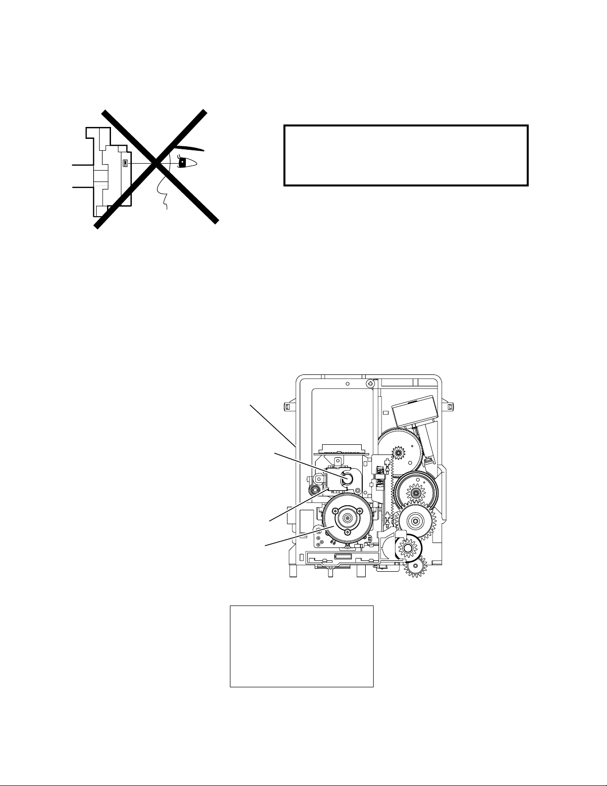
LASER BEAM SAFETY PRECAUTIONS
This DVD player uses a pickup that emits a laser beam.
Do not look directly at the l aser beam coming
from the pickup or allo w it t o str ike agai nst your
skin.
The laser beam is emitted from the locatio n shown in the figure. When ch ecking the laser d iode, be sure to keep
your eyes at least 30cm away from the pickup lens when the diode is tur ned on. Do not loo k directly at the laser
beam.
Caution: Use of controls an d adjustments, or doing pr ocedures other than th ose specified here in, may result in
hazardous radiation exposure.
rive Mecha Assembly
Laser Beam Radiation
Laser Pickup
Turntable
CAUTION
LASER RADIATION
WHEN OPEN. DO NOT
STARE INTO BEAM.
Location: Inside Top of DVD mechanism.
1-2-1 DVD_LASER

IMPORTANT SAFETY PRECAUTIONS
Product Safety Notice
Some electrical and mechanical parts have special
safety-related characteristics which are often not evident from visual inspection, nor can the protection they
give necessarily be obtained by replacing them with
components rated for higher voltage, wattage, etc.
Parts that have special safety characteristics are identified by a # on schematics and in parts lists. Use of a
substitute replacement that does not have the same
safety characteristics as the recommended replacement par t might create shock, fire, and/or other h azards. The Product’s Safety is under review
continuously and new instructions are issued whenever appropriate. Prior to shipment from the factory,
our products are carefully inspected to confirm with
the recognized product safety and electrical codes of
the countries in which they are to be sold. However, in
order to maintain such compli ance, it is equall y impor tant to implement the following precautions when a set
is being serviced.
Precautions during Servicing
A. Parts identified by the # symbol are critical for
safety. Replace only with part number specified.
B. In addition to safety, other parts and assemblies
are specified for conformance with regulations
applying to spurious radiation. These must also be
replaced only with specified re pla ce men ts.
Examples: RF converters, RF cables, noise blocking capacitors, and noise blocking filters, etc.
C. Use specified internal wiring. Note especially:
1)Wires covered with PVC tubing
2)Double insulated wires
3)High voltage leads
D. Use specified insulating materials for hazardous
live parts. Note especially:
1)Insulation tape
2)PVC tubing
3)Spacers
4)Insulators for transistors
E. When replacing AC primary side components
(transformers, power cord, etc.), wrap ends of
wires securely about the terminals before soldering.
F. Observe that the wires do not conta ct heat produc -
ing parts (heats inks, oxide metal fil m resis tors, fusible resistors, etc.).
G. Check that replaced wires do not contact sharp
edges or pointed parts.
H. When a power cord has been replaced, check that
5 - 6 kg of force in any direction will not loosen it.
I. Also check areas surrounding repair ed locations.
J. Be careful that foreign objects (screws, solder
droplets, etc.) do not remain inside the set.
K. Crimp type wire connector
The power transformer uses cri mp type con nector s
which connect the power cord and the primary side
of the transformer. When replacing the transformer,
follow these steps carefully and precisely to prevent
shock hazards.
Replacement procedure
1)Remove the old connector by cutting the wires at a
point close to the connector.
Important: Do not re-use a connector. (Discard it.)
2)Strip about 15 mm of the insulation from the ends
of the wires. If the wires are stranded, twist the
strands to avoid frayed conductors.
3)Align the lengths of the wires to be connected.
Insert the wires fully into the connector.
4)Use a crimping tool to crimp the metal sleeve at its
center. Be sure to crimp fully to t he complete closure of the tool.
L. When connecting or disconnecting the internal
connectors, first, disc onnect the AC plug from the
AC outlet.
1-3-1 DVD_SFN1
r
e)
Safety Check afte r Servicing
Examine the area surrounding the repaired location for
damage or deteri oration. Observe that screws, par ts,
and wires have been returned to their original positions. Afterwards, do the following tests and confirm
the specified values to verify compliance with safety
standards.
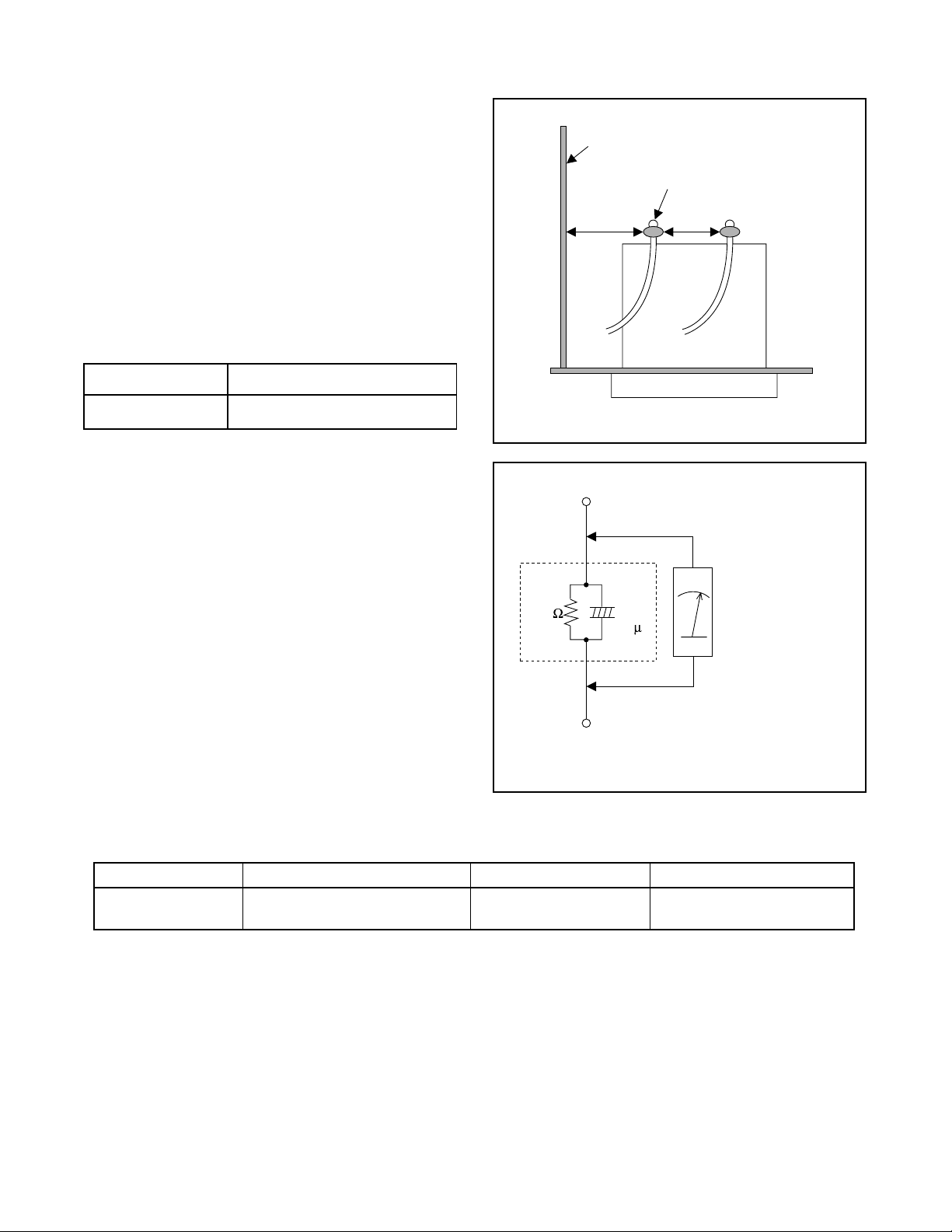
1. Clearance Distance
When replacing primary circuit components, confirm
specified clearanc e distance (d ) and (d’) be tween soldered terminals, and between terminals and surrounding metallic parts. (See Fig. 1)
Table 1 : Ratings for selected area
AC Line Voltage Clearance Distance (d) (d’)
Chassis or Secondary Conducto
Primary Circuit Terminals
dd'
120 V
Note: This table is unofficial and for reference only.
Be sure to confirm the precise values.
2. Leakage Current Test
Confirm the specified (or lower) leakage current
between B (earth ground, power cord plug prongs)
and externally exposed accessible parts (RF terminals, antenna terminals, video and audio input and
output terminals, microphone jacks, earphone jacks,
etc.) is lower than or equal to the specified value in the
table below.
Measuring Method (Power ON) :
Insert load Z between B (earth ground, power cord
plug prongs) and exposed accessible parts. Use an
AC voltmeter to measure across the ter minals of load
Z. See Fig. 2 and the following table.
Table 2: Leakage current ratings for selected areas
AC Line Voltage Load Z Leakage Current (i) Earth Ground (B) to:
120 V
≥ 3.2mm (0.126 inches)
0.15µF CAP. & 1.5kΩ RES.
Connected in parallel
Exposed Accessible Part
Z
1.5k
i≤0.5mA Peak Exposed accessible parts
0.15 F
Earth Ground
B
Power Cord Plug Prongs
AC Voltmeter
(High Impedanc
Fig. 1
Fig. 2
Note: This table is unofficial and for reference only. Be sure to confirm the precise values.
1-3-2 DVD_SFN1
STANDARD NOTES FOR SERVICING
O
P
P
Circuit Board Indications
a. The output pin of the 3 pin Regulator ICs is indi-
cated as shown.
Top View
Input
ut
b. For other ICs, pin 1 and every fifth pin are indicated
as shown.
In
in 1
c. The 1st pin of every ma le c on nec tor i s indi ca ted a s
shown.
in 1
Bottom View
5
10
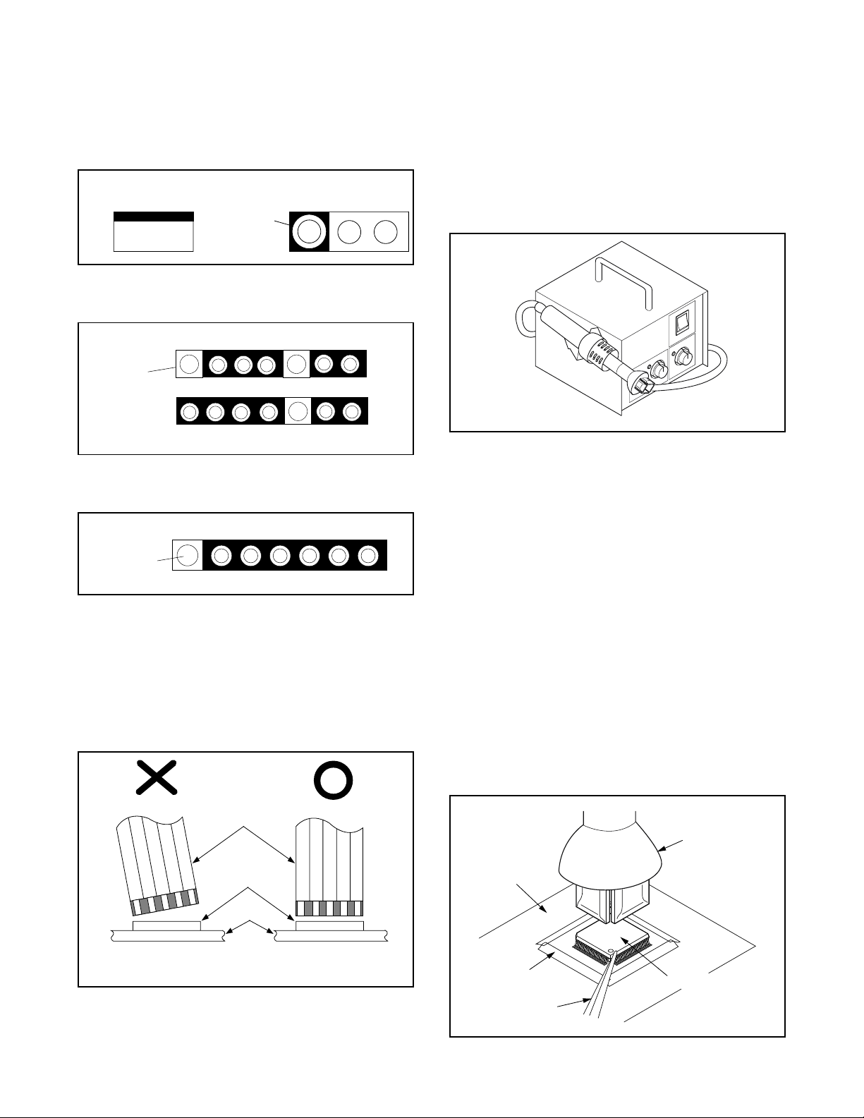
How to Remove / Install Flat Pack-IC
1. Removal
With Hot-Air Flat Pack-IC Desoldering Machine:.
(1) Prepare the hot-air flat pack-IC desoldering
machine, then apply hot air to the Flat Pack-IC
(about 5 to 6 seconds). (Fig. S-1-1)
Fig. S-1-1
(2) Remove the flat pack-IC with tweezers while apply-
ing the hot air.
(3) Bottom of the flat pack-IC i s fixed with glue to the
CBA; when rem oving enti re flat pa ck-IC, first apply
soldering iron to ce nter of the flat pack-IC and hea t
up. Then remove (glue will be melted). (Fig. S-1-6)
(1) Release the flat pack-IC from th e CBA usin g twee-
zers. (Fig. S-1-6)
Caution:
Instructions for Connectors
1. When you conn ect or disconn ect t he FFC (Flexible
Foil Connector) cable, be sure to first disconnect
the AC cord.
2. FFC (Flexible Foil Connector) cable should be
inserted parallel into the connector, not at an angle.
FFC Cable
Connector
CBA
* Be careful to avoid a short circuit.
1. D o not supply hot air to the chip par ts around the
flat pack-IC for over 6 seconds because damage to
the chip parts may occur. Put masking tape around
the flat pack-IC to protect other parts from damage.
(Fig. S-1-2)
2. The flat pack-IC on the CBA is affixed with glue, so
be careful not to brea k or damage the foil of each
pin or the solder lands under the IC when removing
it.
Hot-air
Flat Pack-IC
Desoldering
CBA
Masking
Tape
Tweezers
Machine
Flat Pack-IC
Fig. S-1-2
1-4-1 DVD_NOTE
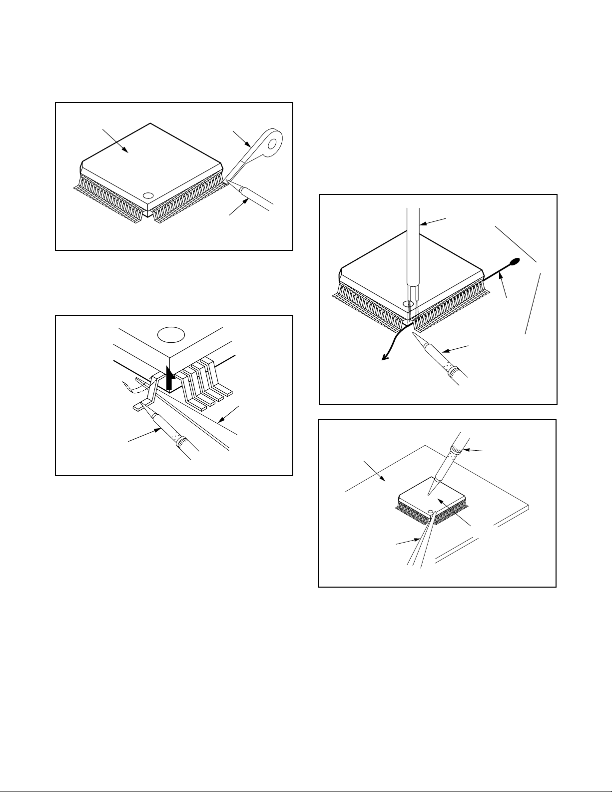
With Soldering Iron:
F
F
S
rp
or
n
(1)Using desoldering braid, remove the sol der from al l
pins of the flat pack-IC. When you use solder flux
which is applied to all pins of the flat pack-IC, you
can remove it easily. (Fig. S-1-3)
lat Pack-IC
Desoldering Braid
(4) Bottom of the flat pack-IC i s fixed with glue to the
CBA; when rem oving enti re flat pa ck-IC, first apply
soldering iron to ce nter of the flat pack-IC and hea t
up. Then remove (glue will be melted). (Fig. S-1-6)
(5) Release the flat pack-IC from th e CBA usin g twee-
zers. (Fig. S-1-6)
Note:
When using a solder ing iron, care must be taken
to ensure that the flat pack-IC is not bei ng held by
glue. When the flat pack-IC is removed from the
CBA, handle it gently beca use it may be damaged
if force is applied.
Soldering Iron
Hot Air Blower
Fig. S-1-3
(2) Lift each lead of the flat pack-IC upward one by
one, using a shar p pin or wire to which s older will
not adhere (iron wi re). When he ating the pins, us e
a fine tip soldering iron or a hot air desoldering
machine. (Fig. S-1-4)
Iron Wire
Soldering Iron
To Solid
Mounting Point
Fig. S-1-5
Sha
Pin
ine Tip
oldering Iron
Fig. S-1-4
CBA
Fine Tip
Soldering Iro
(3)B ottom of the flat pack-IC is fixed with glue to the
CBA; when removing entire flat pack-IC, first apply
soldering iron to c en ter of the flat pack-IC and heat
up. Then remove (glue will be melted). (Fig. S-1-6)
(4)Re lease the fl at pack-IC from the CBA using twee-
zers. (Fig. S-1-6)
Tweezers
Flat Pack-IC
With Iron Wire:
(1)Using desoldering braid, remove the sol der from al l
Fig. S-1-6
pins of the flat pack-IC. When you use solder flux
which is applied to all pins of the flat pack-IC, you
can remove it easily. (Fig. S-1-3)
(2) Affix the wire to a workbench or solid mounting
point, as shown in Fig. S-1-5.
(3) While heating the pins using a fine tip soldering
iron or hot air blower, pull up the wire as the solde r
melts so as to lift the IC leads from the CBA contact
pads as shown in Fig. S-1-5
1-4-2 DVD_NOTE
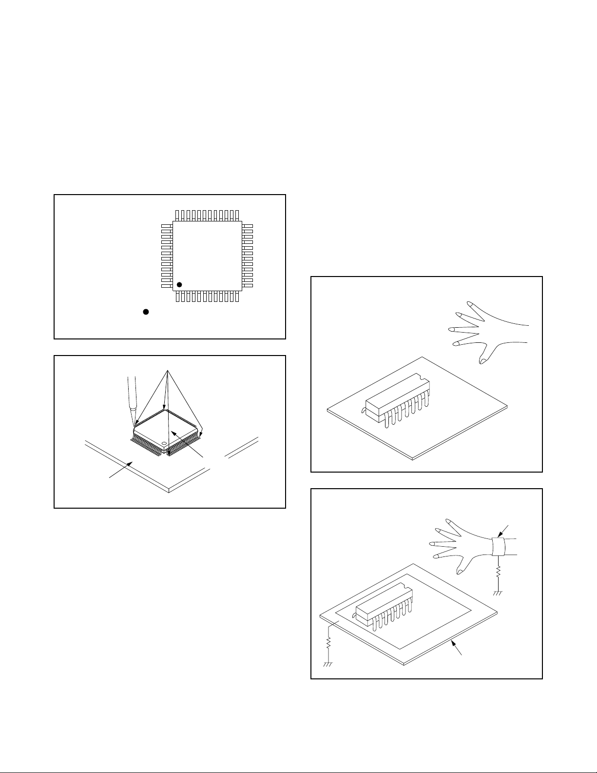
2. Installation
P
i
d
(1) Using desoldering braid, remove the solder from
the foil of each pin of the flat pack-IC on the CBA
so you can install a replacement fla t pack-IC more
easily.
(2) The “I” mark on the flat pack-IC indicates pin 1.
(See Fig. S-1-7.) Be s ure this mark matches the 1
on the PCB when positioni ng for installation. Then
presolder the four cor ners of the fl at pack-IC. (See
Fig. S-1-8.)
(3)Solder all pins of the flat pack-IC. Be sure that none
of the pins have solder bridges.
Example :
in 1 of the Flat Pack-IC
s indicated by a " " mark.
Fig. S-1-7
Instructions for Handling
Semi-conductors
Electrostatic breakdown of the semi-conductors may
occur due to a potential di fference caused by electrostatic charge during unpacking or repair work.
1. Ground for Human Body
Be sure to wear a groun ding band (1M Ω) that is properly grounded to re move any static electr ici ty that may
be charged on the body.
2. Ground for Workbench
(4) Be sure to place a conductive sheet or copper plate
with proper grounding (1MΩ) on the workbench or
other surface, where the semi-conductors are to be
placed. Because the static electricity charge on
clothing will not escape thr ough the body grounding band, be careful t o avoid contacting semi-conductors with your clothing.
< Incorrect >
CBA
Presolder
Flat Pack-IC
Fig. S-1-8
CBA
< Correct >
Grounding Ban
1MΩ
CBA
1MΩ
Conductive Sheet or
Copper Plate
1-4-3 DVD_NOTE
PREPARATION FOR SERVICING
How to Enter the Service Mode
About Optical Sensors
Caution:
An optical sensor system is used for the Tape Start
and End Sensors on this equipment. Carefully read
and follow the instructions below. Otherwise the unit
may operate erratically.
What to do for preparation
Insert a tap e into the Deck Mechan ism Assembly and
press the PLAY button. The tape will be loaded into
the Deck Mechanism Assembly. Make sure the power
is on, TP502 (SENSOR INHIBITION) to GND. This will
stop the function of Tape Start Sensor, Tap e E nd Sen sor and Reel Sensors. (If these TPs are connected
before plugging in the unit, the function of the sens ors
will stay valid.) See Fig. 1.
Q503
Q504
TP502
S-INH
Fig. 1
Note: Because the Tape End Sensors are inactive, do
not run a tape all the way to the start or the en d of the
tape to avoid tape damage.
1-5-1 H9400PFS
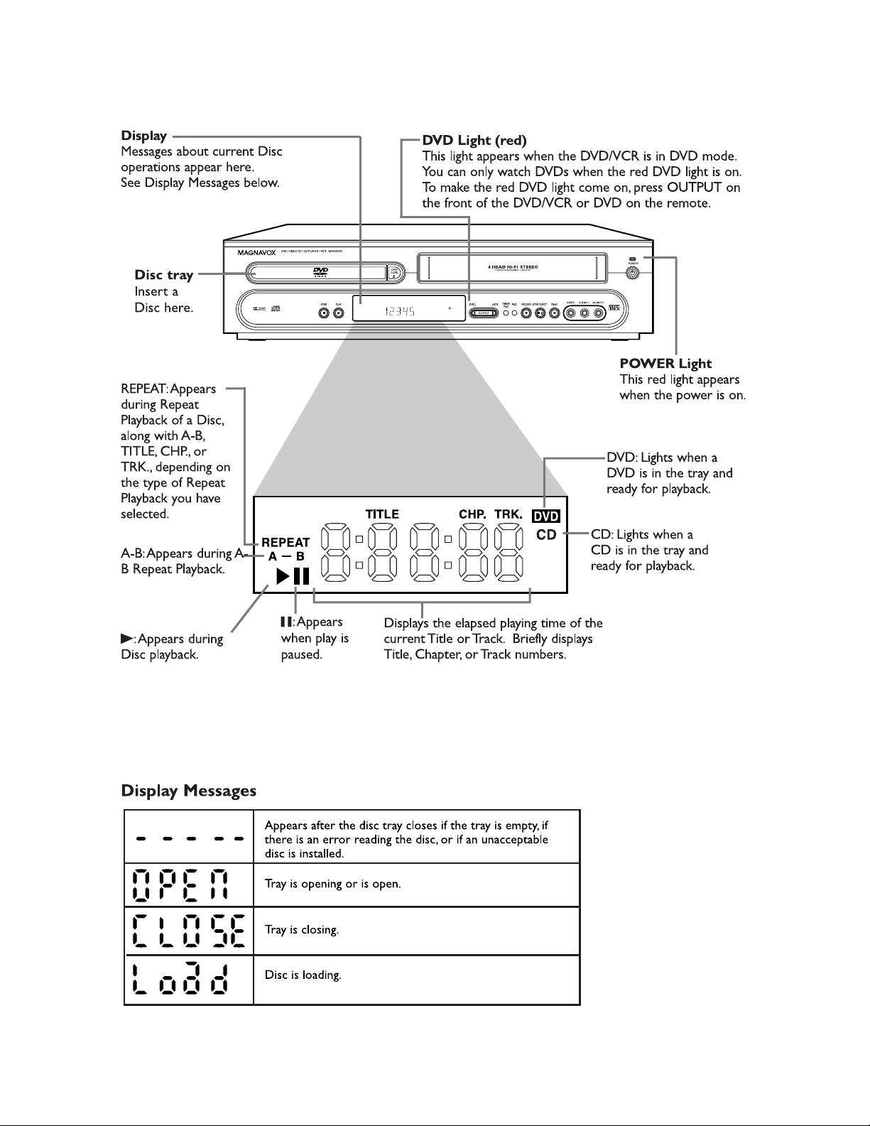
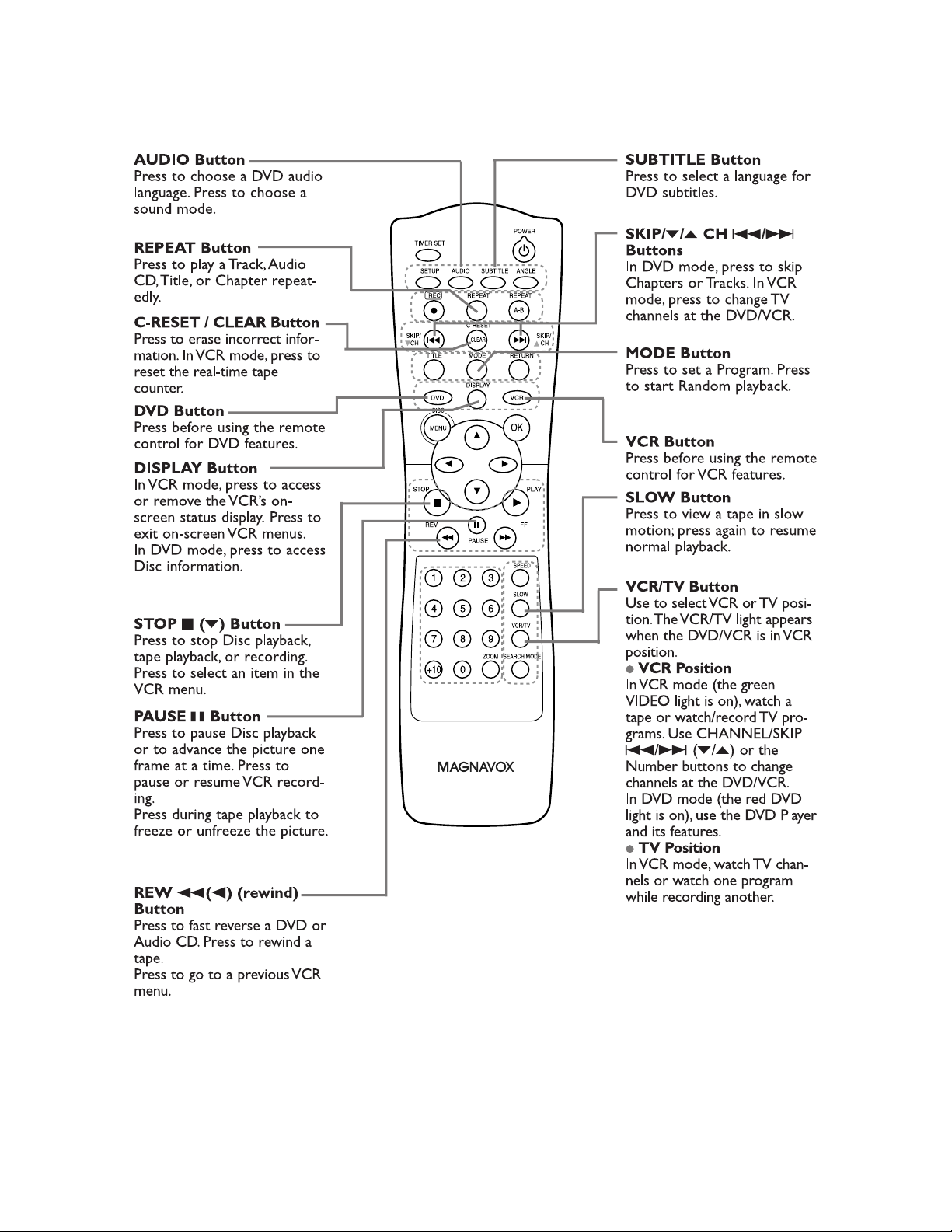
OPERATING CONTROLS AND FUNCTIONS
1-6-1 H9460IB
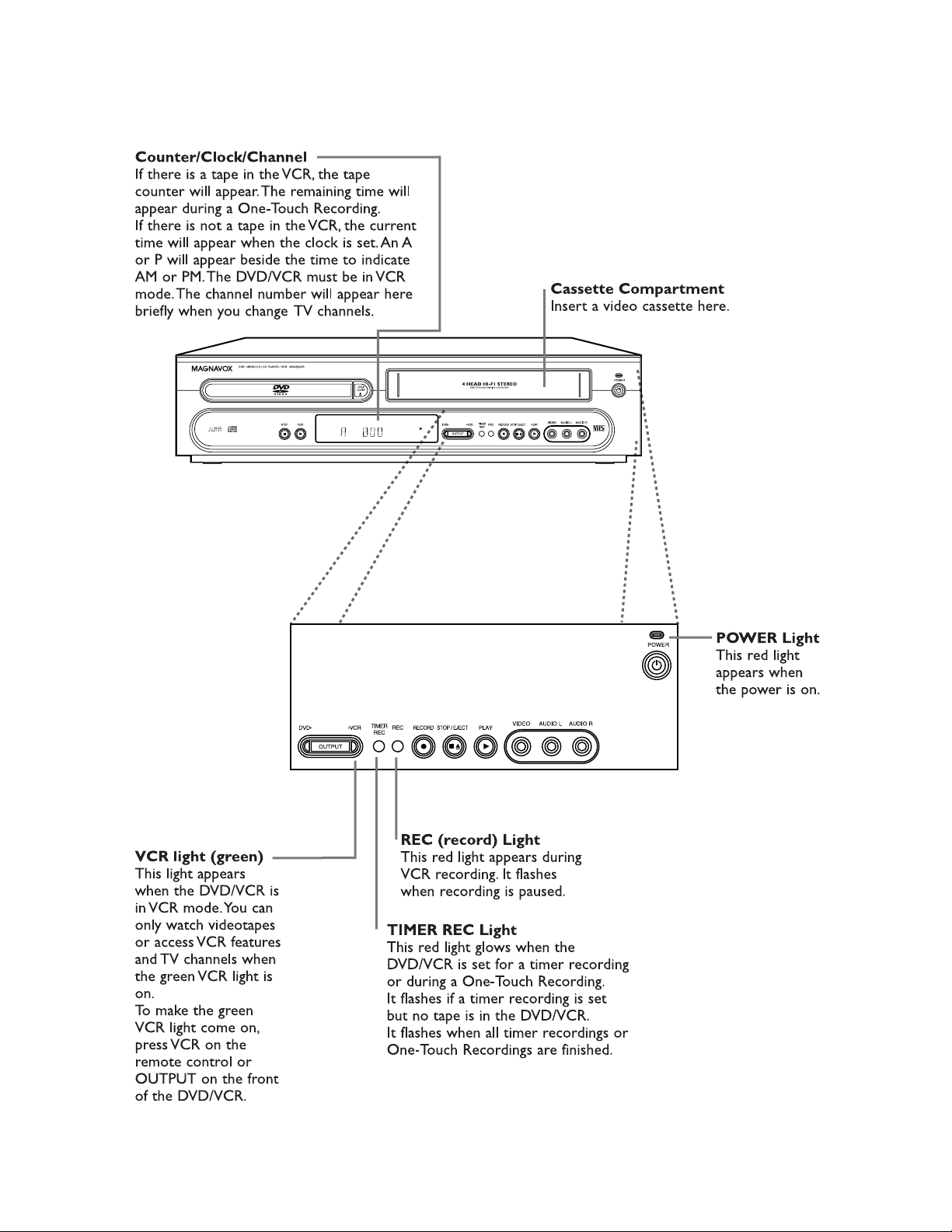
1-6-2 H9460IB
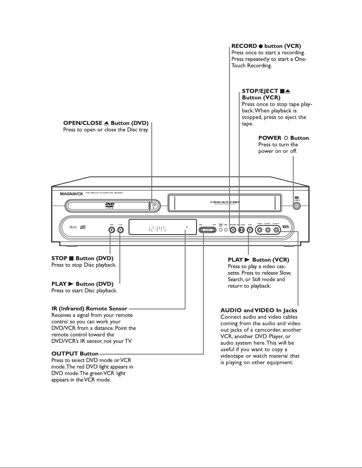
1-6-3 H9460IB
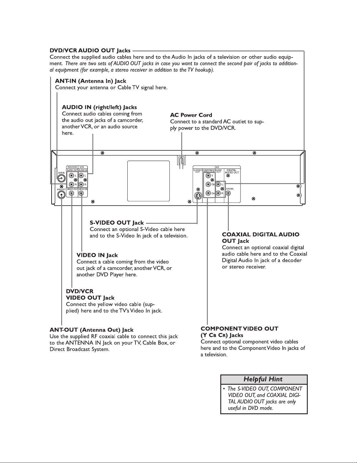
1-6-4 H9460IB
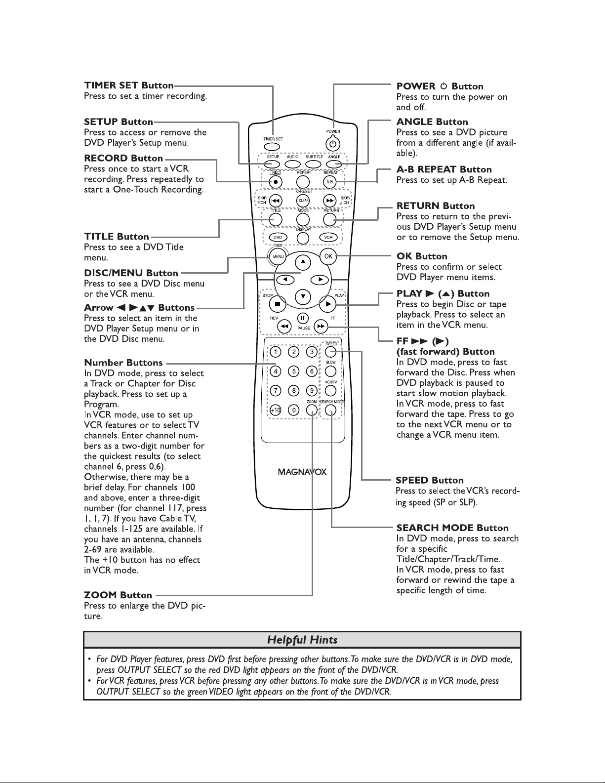
REMOTE CONTROL OPERATION
1-7-1 H9460IBR
1-7-2 H9460IBR
CABINET DISASSEMBLY INSTRUCTIONS
1. Disassembly Flowchart
This flowchart indicates the disassembly steps to gain
access to item(s) to be ser vic ed. When reasse mbling,
follow the steps in reverse order. Bend, route, and
dress the cables as they were originally.
[1] Top Cover
[2] Front
Assembly
[16] Side
Bracket
[5] DVD Main
CBA Unit
[13] DVD OP/CL
CBA
[12] Main CBA
[14] Function
CBA
[3] Top Bracket
[4] DVD Mecha
Assembly
[6] Rear Unit
[10] VCR
Chassis Unit
[15] Deck
Pedestal
[9] Rear Panel
[8] PCB Bracket
[7] Power
Supply CBA
[11] Deck
Assembly
2. Disassembly Method
REMOVAL
ID/
LOC.
No.
[1] Top Cover D1 7(S-1) -
[2]
[3]
[4]
[5]
PART
Front
Assembly
Top
Bracket
DVD
Mecha
Assembly
DVD Main
CBA Unit
REMOVE/*UNHOOK/
Fig.
UNLOCK/RELEASE/
No.
UNPLUG/DESOLDER
D2 (S-3), *7(L-1)
D2 4(S-2) -
3(S-4), *CN401,
D3
*CN302, *CN601
2(S-5), *CN201,
D4
*CN301
Note
1
1-1
1-2
-
2
2-1
2-2
2-3
3
REMOVAL
ID/
LOC.
No.
[7]
[8]
[9]
[10]
[11]
[12] Main CBA D8 ---------- -
[13]
[14]
[15]
[16]
↓
(1)
Note:
(1): Identification (location) No. of parts in the figures
(2):Name of the part
(3):Figure Number for reference
(4): Identification of parts to be removed, unhooked,
(5): Refer to “Reference Notes.”
PART
Power
Suppy CBA
PCB
Brackt
Rear Panel
VCR
Chassis
Unit
Deck
Assembly
DVD OP/
CL CBA
Function
CBA
Deck
Pedestal
Side
Bracket
↓
(2)
unlocked, released, unplugged, unclamped, or
desoldered.
P=Spring, L=Locking Tab, S=Screw,
CN=Connector
*=Unhook, Unlock, Release, Unplug, or Desolder
e.g. 2(S-2) = two Screws (S-2),
2(L-2) = two Locking Tabs (L-2)
REMOVE/*UNHOOK/
Fig.
UNLOCK/RELEASE/
No.
UNPLUG/DESOLDER
D6 4(S-8) -
D6 3(S-9) -
D6 ---------- -
D7 5(S-10), 4(S-11) -
D8 Desolder, 2(S-12) 4,5
D8 ---------- -
D8 ---------- -
D9 7(S-13) -
D9 (S-14) -
↓
(3)
↓
(4)
Note
(5)
↓
[6] Rear Unit D5
5(S-6), 3(S-7),
CN1005
-
1-8-1 H9460DC
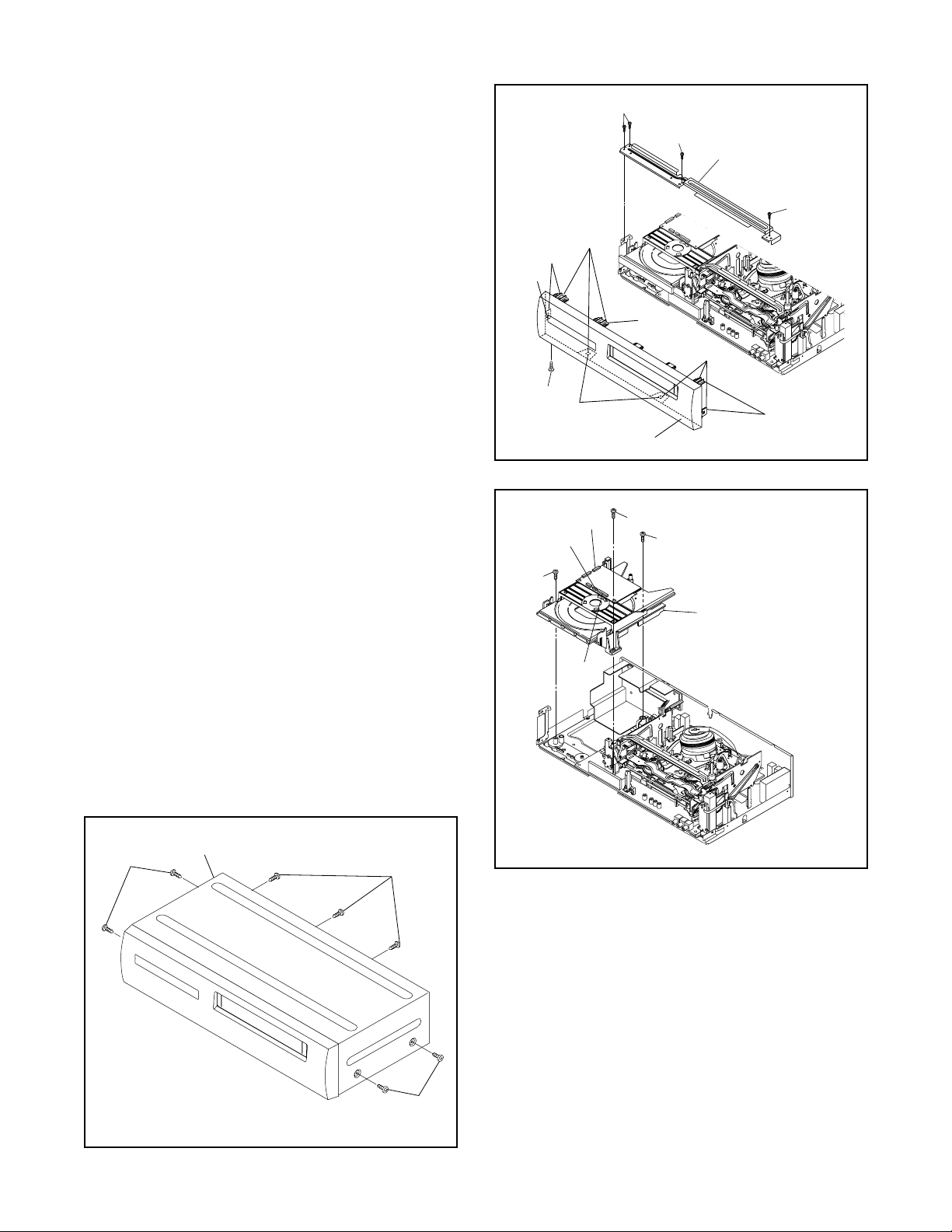
Reference Notes
(
(
ly
CAUTION 1: Locking Tabs (L -1) are fra gile. Be caref ul
not to break them.
1-1. Remove Screw (S-3).
1-2. Release seven Locking Tabs (L-1) (to do this, first
release five Locking Tabs (A) at the side and top,
and then release two Locking Tabs (B) at the bottom.)
CAUTION 2: Electrostatic breakdown of the laser
diode in the optical system block may occur as a
potential difference caused by electrostatic charge
accumulated on cloth, human body etc., during
unpacking or repair work.
To avoid damage of pickup follow next procedures.
2-1. Slide the pickup unit as shown in Fig. D4.
2-2. Short the three short lands of FPC cable with sol-
der before removing the FFC cable (CN301) from
it. If you disconnect the FFC ca ble (CN301), the
laser diode of pickup will be destroyed. (Fig. D4)
2-3. Disconnect Connector (CN201). Remove two
Screws (S-5) and lift the DVD Main CBA Unit.
(Fig. D4)
CAUTION 3: When reassembling, confirm the FFC
cable (CN301) is conne cted compl etely. Then remove
the solder from the three short lands of FPC cable.
(Fig. D4)
4. When re ass em bling, s old er wire j ump er s a s s hown
in Fig. D8.
5. Before installing the Deck Assembly, be sure to
place the pin of LD-SW on M ain CBA as shown in
Fig. D8. Then, install the Deck Assembly while
aligning the hole of Cam Gear with the pin of LDSW, the shaft of Cam Gear with the hole of LD -S W
as shown in Fig. D8.
(L-1)
(A)
L-1)
(S-3)
(B)
[2] Front Assembly
CN601
CN302
S-4)
CN401
(S-2)
(S-2)
[3] T op Bracket
(S-2)
(A)
(L-1)
(A)
Fig. D2
(S-4)
(S-4)
[4] DVD Mecha Assemb
[1] T op Cover
(S-1)
(S-1)
(S-1)
Fig. D3
Fig. D1
1-8-2 H9460DC
(S-5)
6)
)
l
(
0)
CN301
CN201
(S-5)
[5] DVD Main
(S-9)
CBA Unit
[9] Rear Pane
(S-8)
[8] PCB Bracket
[7] Power Supply CBA
DVD Mecha
(S-8)
Fig. D6
A
Slide
[6] Rear Unit
B
Pickup Unit
View for A
Short the three short
lands by soldering
View for B
(S-7)
CN1005
(S-6)
Fig. D4
(S-7)
(S-
(S-10)
S-11)
[10] VCR Chassis Unit
(S-11)
(S-11)
(S-10)
(S-11)
(S-1
Fig. D7
(S-7
Fig. D5
1-8-3 H9460DC
FE Head
[11] Deck
Assembly
Desolder
Lead with
blue stripe
[13] DVD OP/CL CBA
(S-12)
[14] Function CBA
Cylinder Assembly
AC Head
Assembly
[12] Main CBA
(S-12)
Desolder
[11] Deck Assembly
Shaft
Hole
LD-SW
Lead with
blue stripe
Pin
SW507
LD-SW
[12] Main CBA
Cam Gear
Hole
Pin
[12] Main CBA
From
AC Head
Assembly
From
Capstan
Motor
Assembly
From
Cylinder
Assembly
Printing side
Desolder
Lead with
blue stripe
Desolder
BOTT OM VIEW
Lead connections of Deck Assembly and Main CBA
From
FE Head
Lead with
white stripe
Fig. D8
1-8-4 H9460DC
[15] Deck Pedestal
D
(S-13)
(S-14)
[16] Side
Bracket
(S-13)
HOW TO MANUAL EJECT
Fig. D9
1. Remove the Top Case.
2. Rotate this roulette in the direction of the arrow as
shown below.
Top Cover
1
VD Mecha
Tray
Deck Assembly
Rotate this roulette in
3
2
the direction of the arrow
2
1-8-5 H9460DC
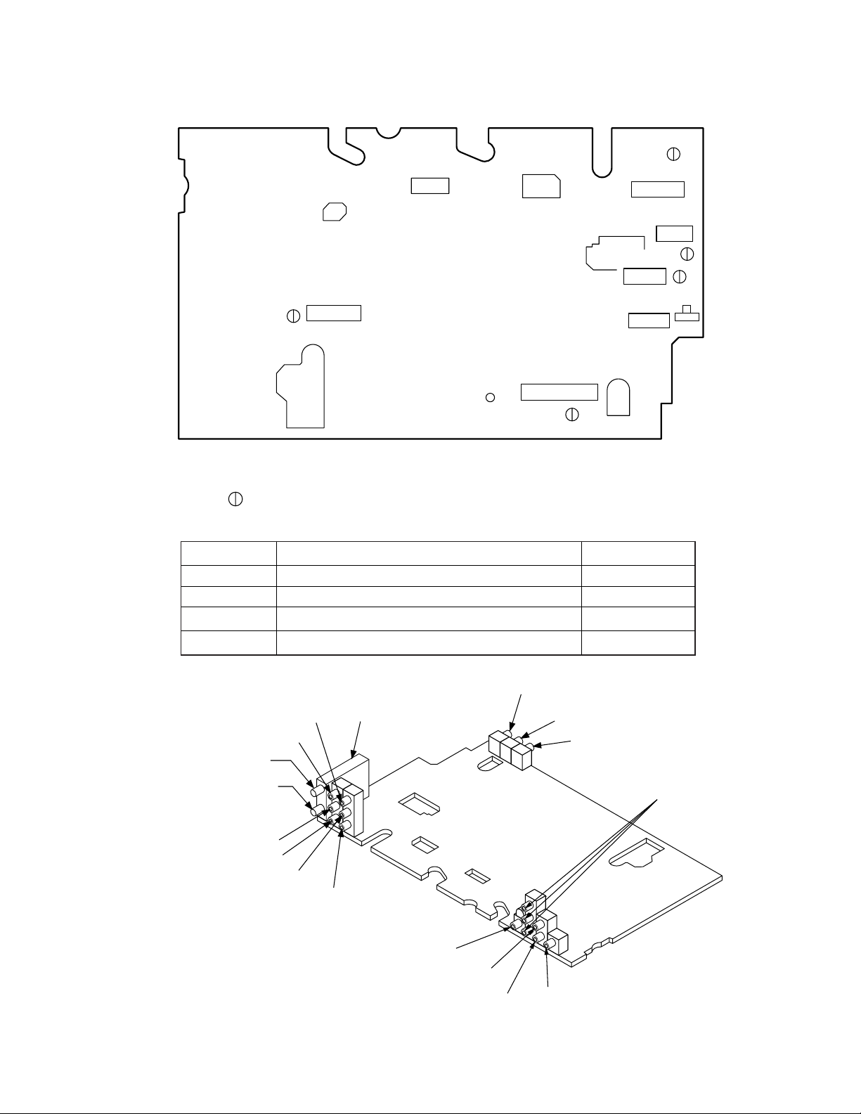
ELECTRICAL ADJUSTMENT INSTRUCTIONS
e
2
)
C
C
c
General Note: "CBA" is an abbreviation for
"Circuit Board Assembly."
NOTE:
1.Electric al adjust ments are required a fter repla cing
circuit components and ce rtain mechanical par ts.
It is impor tant to do these adjustments only afte r
all repairs and replacements have been completed. Also, do not attempt these adjustments
unless the proper equipment is available.
2.To perform these alignment / confi rmation procedures, make sure that the tracking control is set in
the center position: P ress ei ther "CHA NNEL L5??" or
"CHANNEL K" button on th e front panel first , then
the "PLAY" button on the front panel.
H1
H2
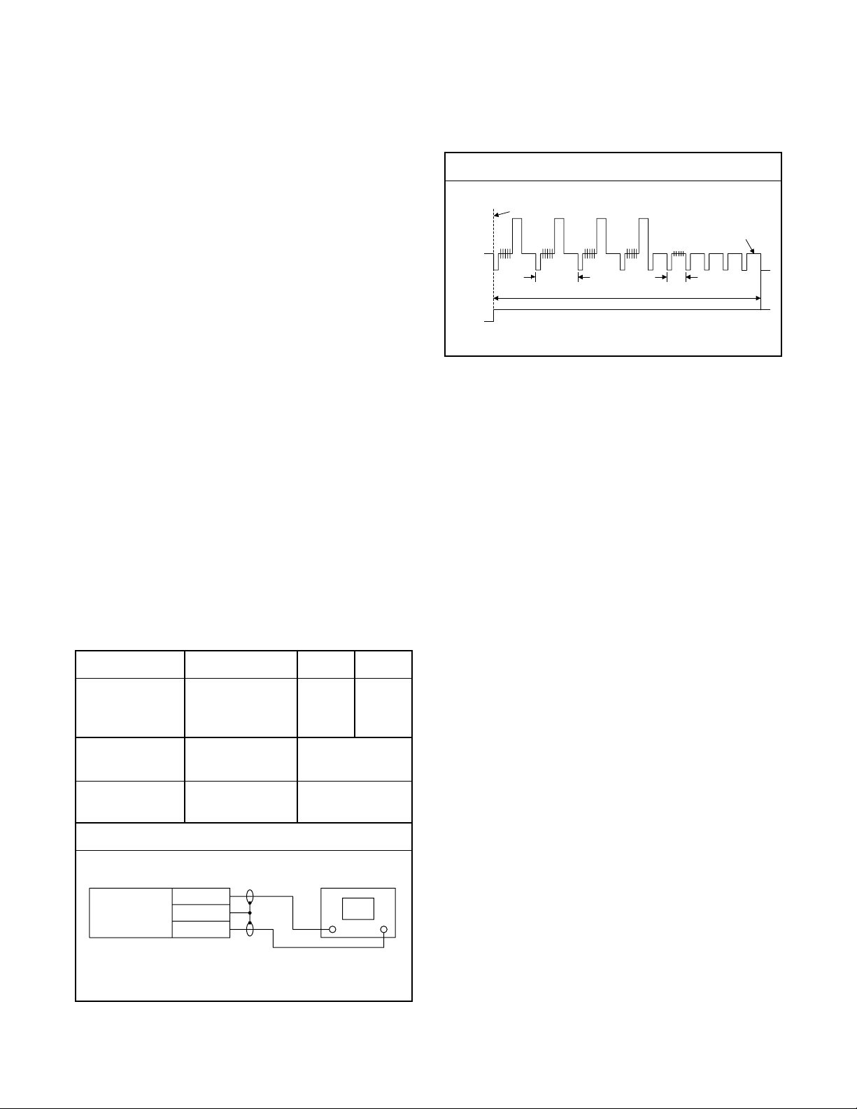
Figure 1
EXT. Syncronize Trigger Point
1.0H
Switching Pulse
6.5H
V-Syn
0.5H
Test Equipment Required
1.Oscilloscope: Dual-trace with 10:1 probe,
V-Range: 0.001~50V/Div.,
F-Range: DC~AC-20MHz
2.Alignment Tape (VFMS0001H6)
Head Switching Po sition Adjustment
Purpose:
To determine the Head Switching point during
playback.
Symptom of Mi sadjustm e n t:
May cause Head Switching noise or ver tical jitter
in the picture.
Test point Adj.Point Mode Input
TP751(V-OUT)
TP302(RF-SW)
GND
Tape
VR501
(Switching Point)
(MAIN CBA)
Measurement
Equipment
PLAY
(SP)
Spec.
Reference Notes:
Playback the Alignment tape and adjust VR501 so that
the V-sync front edge of the CH1 video output waveform is at the 6.5H(412 .7µs) del ayed position from the
rising edge of the CH2 head switching pulse waveform.
-----
VFMS0001H6 Oscilloscope
Connections of Measurement Equipment
TP751
Main CBA
GND
TP302
6.5H±1H
(412.7µs±60µs)
Oscilloscop
CH1 CH
Trig. (+
1-9-1 H9460EA
D
t
Adjustment Points and Test Points
Main CBA Top View
TP302
RF-SW
TP751
V-OUT
TP513
CTL
TP301
C-PB
VR501
SW-P
TP502
SENS-INH
TEST POINT INFORMATION
: Indicates a test point with a jumper wire across a hole in the PCB.
TEST POINTS NOT USED IN ELECTRICAL ADJUSTMENTS
Test Point
TP301
TP302
TP513
TP502
DVD/VCR Audio L In
DVD/VCR Audio L Out
Antenna In
Antenna Out
VD/VCR Audio R Out
DVD/VCR Video Out
DVD/VCR Audio R In
DVD/VCR Video In
Used in: Page No.
Mechanical Alignment Procedures
Mechanical Alignment Procedures
Mechanical Alignment Procedures
Preparation for Servicing
DVD/VCR Audio R In
Tuner Unit
2-3-3, 2-3-4
2-3-3, 2-3-4
2-3-3
1-5-1
DVD/VCR Audio L In
DVD/VCR Video In
Componen
Video Out
S-Video Out
DVD Audio L Out
DVD Audio R Out
1-9-2 H9460EA
Digital Audio Out
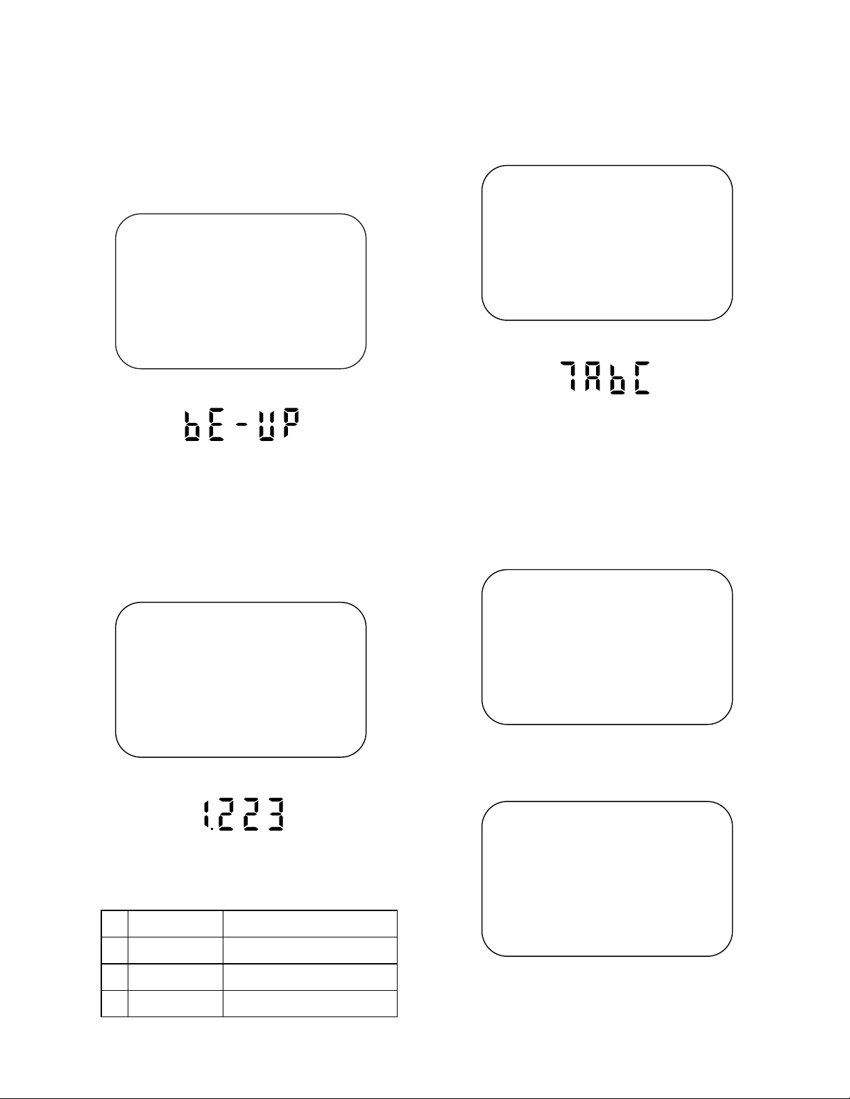
FIRMWARE RENEWAL MODE
F
e
F
e)
F
e)
1. Turn the power on and remove the disc on the tray.
2. To put the DVD p layer into version up mode, press
[9], [8], [7], [6], and [SEARCH MO DE] buttons on
the remote control unit in that order. The tray will
open automatically.
Fig. a appears on the screen and Fig. b appears on
the VFD.
F/W Version Up Mode
Please insert a DISC
for F/W Version Up.
EXIT: POWER
Fig. a Version Up Mode Screen
ig. b VFD in Version Up Mod
The DVD player can also enter the version up
mode with the tray open. In this case, Fig. a will be
shown on the screen while the tray is open.
3. Load the disc for version up.
4. The DVD player enters the F/W version up mode
automatically. Fig. c appears on the screen and
Fig. d appears on the VFD.
F/W Version Up Mode
VERSION : ********
Reading...(*2)
5. A fter programming is fini shed, the tray opens au tomatically. Fig. e appears on the screen and the
checksum in (*3) of Fig. e appears on the VFD.
(Fig. f)
F/W Version Up Mode
VERSION : ********
Completed
SUM : 7abc (*3)
Fig. e Completed Program Mode Screen
ig. f VFD upon Finishing the Programming Mode (Exampl
At this time, no buttons are available.
6. Unplug the AC cord from the AC outlet. Then plug it
again.
7. Turn the power on by pressing the power button
and the tray will close.
8. Press [1], [2], [3], [4], and [DISPLAY] buttons on the
remote control unit in that order.
Fig. g appears on the screen.
model: ****** Ver: **** Region: **
1: VFD TEST
2: TT REPEAT PLAY
3: EEPROM CLEAR
4: MEASUREMENT SERVO
5: DISC READ CHECK
6: MECHA CHECK
7: DISC INFO
8: ERROR RATE
EXIT: POWERRETURN: -----
EXIT: POWER
Fig. c Programming Mode Screen
ig. d VFD in Programming Mode (Exampl
9. Press [3] button on the remote control unit.
Fig. h appears on the screen.
model: ****** Ver: **** Region: **
TEST 3: EEPROM CLEAR
EEPROM CLEAR: OK
Fig. g
The appearance shown in (*2) of Fig. c is
described as follows:
AppearanceNo. State
Reading... Sending files into the memory
1
Erasing... Erasing previous version data
2
Programming...
3 Writing new version data
10.To finish this mode, press [POWER] button.
1-10-1 H9460TEST
Fig. h
EXIT: POWERRETURN: -----
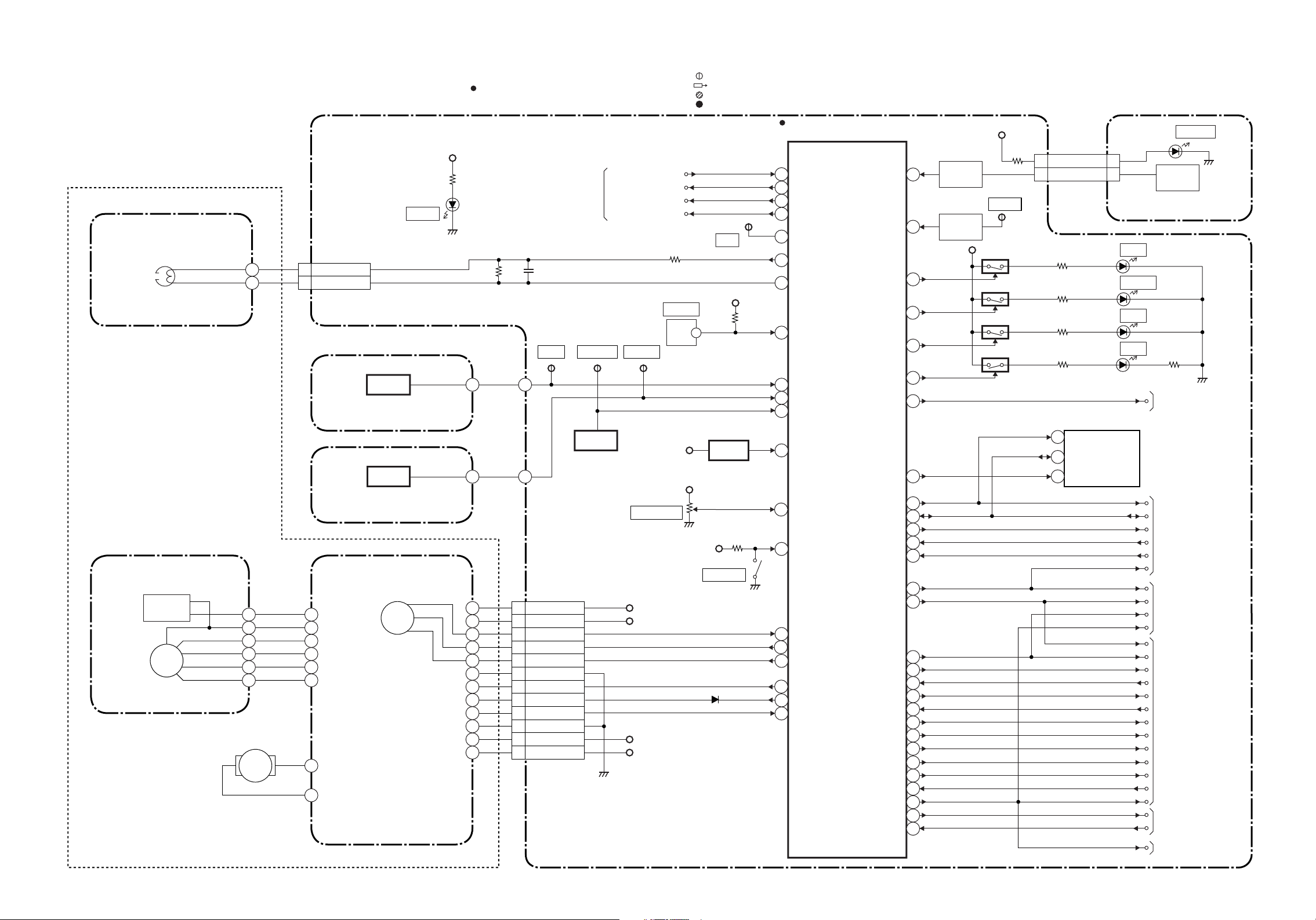
Servo/System Control Block Diagram
NOTE FOR WIRE CONNECTORS:
1. PREFIX SYMBOL "CN" MEANS CONNECTOR.
(CAN DISCONNECT AND RECONNECT.)
2. PREFIX SYMBOL "CL" MEANS WIRE-SOLDER
HOLES OF THE PCB.
(WIRE IS SOLDERED DIRECTLY.)
(DECK ASSEMBLY)
AC HEAD ASSEMBLY
CN504
CONTROL
HEAD
CYLINDER ASSEMBLY
PG
SENSOR
DRUM
MOTOR
M
LOADING
MOTOR
M
CL504
5 CTL(+)
6 CTL(-)
CAPSTAN
MOTOR
MAIN CBA
D555
S-LED
Q504
ST-S
SENSOR CBA
Q503
END-S
SENSOR CBA
CAPSTAN MOTOR
M
AL+5V
BLOCK DIAGRAMS <VCR SECTION>
" " = SMD
FROM/TO DVD SYSTEM
CONTROL BLOCK
DIAGRAM
<DVD SECTION>
1 AL+12V
2 P-ON+5V
3 C-FG
C-F/R
4
C-CONT
5
GND
6
LM-FWD/REV
7
D-CONT
8
D-PFG
9
GND
10
AL+12V
11
AL+15V
12
TP506
ST-S
CL502
TP505
T-REEL
Q506
T-REEL
TEST POINT INFORMATION
REMOTE-VIDEO
DISPLAY-CLK
DISPLAY-DATA
DISPLAY-ENA
SW512
LD-SW
TP507
END-S
TIMER+5V
VR501
SW-POINT
AL+12V
P-ON+5V
AL+12V
AL+15V
:INDICATES A TEST POINT WITH A JUMPER WIRE ACROSS A HOLE IN THE PCB.
:USED TO INDICATE A TEST POINT WITH A COMPONENT LEAD ON FOIL SIDE.
:USED TO INDICATE A TEST POINT WITH NO TEST PIN.
:USED TO INDICATE A TEST POINT WITH A TEST PIN.
IC501
(SERVO/SYSTEM CONTROL)
REMOTE-VIDEO
5
DISPLAY-CLK
6
DISPLAY-DATA
8
DISPLAY-ENA
9
TP513
CTL
AL+5V
Q501
RESET
AL+5V
AL+5V
SW511
REC SW
58
CTL
56
CTL(+)
57
CTL(-)
LD-SW68
69
ST-S
62
END-S
T-REEL
3
RESET
20
PG-DELAY
65
REC-
2
SAF-SW
49
C-FG
C-F/R
27
C-CONT
28
LM-FWD/REV
21
D-CONT29
D-PFG
47
KEY- 1
KEY- 2
REC-IND
TIMER-IND 75
VCR-IND 70
DVD-IND 71
DVD-POWER
VCR/TV
IIC-BUS SDA
Hi-Fi-H-SW
Hi-Fi/NOR-IN
ST/SAP-IN
A-MUTE-H
D-REC-H
D-PB-L
INSEL/ST-SL
C-SYNC
D-V SYNC
V-ENV
C-ROTA
RF-SW
TRICK-H
H-A-SW
H-A-COMP
OUTPUT-SELECT
P-ON-L
P-DOWN-L
67
66
72
26
77
13IIC-BUS SCL
12
25
59
61
24
23
16
41
19
64
78
18
11
14SP/LP/SLP
79
80
46
22
POWER
P-ON+9V
CL508CL509
KEY
SWITCH
TP502
S-INH
KEY
SWITCH
AL+5V
7
1
1 1POWER-LED
2 2KEY-1
Q565
Q563
Q566
Q567
D565
D564 TIMER
D566 VCR
D567 DVD
DVD POWER
TU701(TUNER UNIT)
CLOCK
11
DATA
12
VCR/TV5
IIC-BUS SCL
IIC-BUS SDA
Hi-Fi-H-SW
NORMAL-H
ST/SAP-MODE
A-MUTE-H
A-MUTE-H
D-REC-H
D-PB-L
OUTPUT-SELECT
D-REC-H
D-PB-L
INSEL/ST-SL
C-SYNC
D-V SYNC
V-ENV
C-ROTA
RF-SW
TRICK-H
SP/LP/SLP
H-A-SW
H-A-COMP
OUTPUT-SELECT
P-ON-L
P-DOWN-L
OUTPUT-SELECT
D561
KEY
SWITCH
FUNCTION CBA
REC
TO DVD SYSTEM
CONTROL BLOCK
DIAGRAM
<DVD SECTION>
FROM/TO
Hi-Fi AUDIO
BLOCK
TO AUDIO
BLOCK
FROM/TO
VIDEO BLOCK
FROM/TO POWER
SUPPLY BLOCK
TO DVD SYSTEM
CONTROL BLOCK
DIAGRAM
1-11-1 1-11-2 H9460BLS
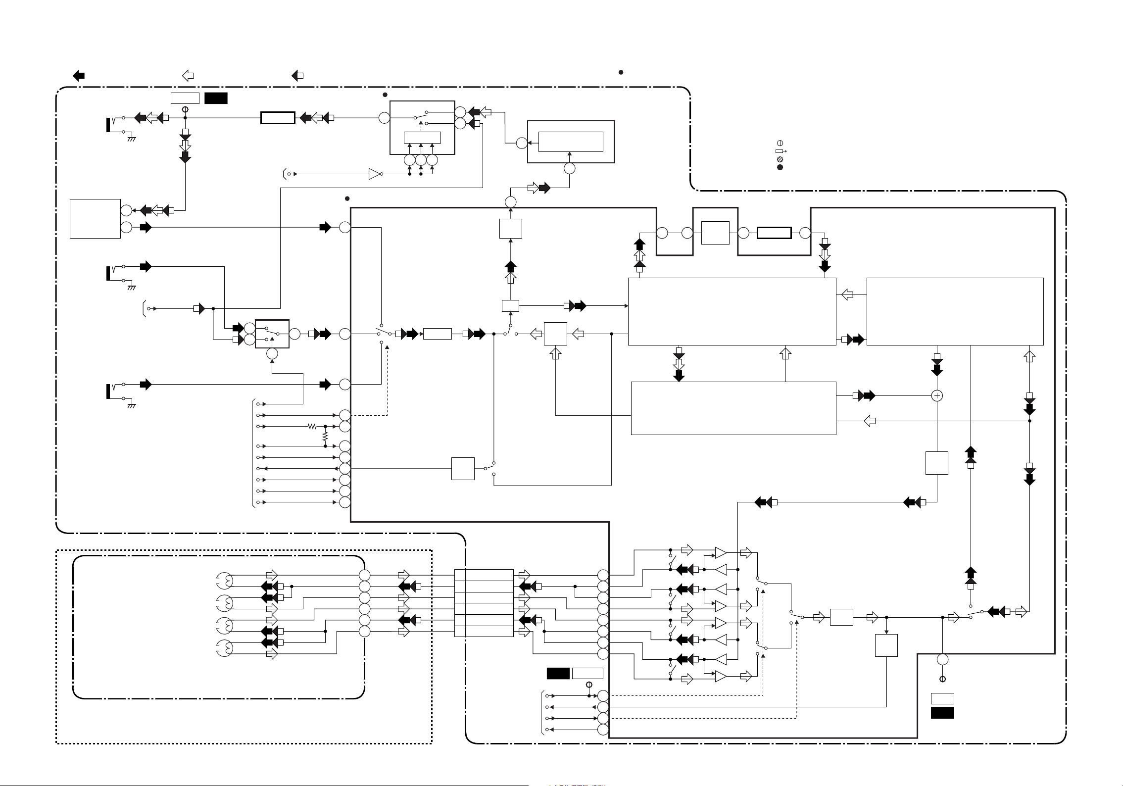
Video Block Diagram
REC VIDEO SIGNAL PB VIDEO SIGNAL DVD VIDEO SIGNAL MODE: SP/REC
TP751
V-OUT
WF1
IC751
Q391
JK751
BUFFER
15
V-OUT
SW CTL
FROM
SERVO/SYSTEM
CONTROL BLOCK
OUTPUT-SELECT
Q760
9 10 11
DIAGRAM
TU701
(Y/C PROCESS)
42
IC301
TUNER
VIDEO IN
VIDEO OUT
6
18
JK752
REAR
V-IN
FROM DVD
VIDEO/AUDIO
BLOCK DIAGRAM
<DVD SECTION>
DVD-VIDEO
IC302 (SW)
1
3
7
38
REAR
2
(OUTPUT SELECT)
VCR
1
DVD
2
V-AGC
35
6dB
AMP
FBC
R P
IC501
OSD CHARACTER
38
MIX
(OSD)
Y/C
MIX
40
" " = SMD
MAIN CBA
NOTE FOR WIRE CONNECTORS:
1. PREFIX SYMBOL "CN" MEANS CONNECTOR.
(CAN DISCONNECT AND RECONNECT.)
2. PREFIX SYMBOL "CL" MEANS WIRE-SOLDER
HOLES OF THE PCB.
(WIRE IS SOLDERED DIRECTLY.)
TEST POINT INFORMATION
45 47 49 44
CCD 1H
DELAY
DOC YNR Y/C COMB
:INDICATES A TEST POINT WITH A JUMPER WIRE ACROSS A HOLE IN THE PCB.
:USED TO INDICATE A TEST POINT WITH A COMPONENT LEAD ON FOIL SIDE.
:USED TO INDICATE A TEST POINT WITH NO TEST PIN.
:USED TO INDICATE A TEST POINT WITH A TEST PIN.
Q301
BUFFER
LUMINANCE
SIGNAL PROCESS
JK753
FRONT
V-IN
(DECK ASSEMBLY)
FROM/TO
SERVO/SYSTEM
CONTROL BLOCK
DIAGRAM
VIDEO (R)-1 HEAD
VIDEO (L)-1 HEAD
VIDEO (L)-2 HEAD
VIDEO (R)-2 HEAD
CYLINDER ASSEMBLY
INSEL2
INSEL/ST-SL
D-PB-L
D-REC-H
TRICK-H
C-SYNC
C-ROTA
D-V SYNC
SP/LP/SLP
FRONT
40
71
16
REC/EE/PB
D-REC-H
11
TRICK
73
34
C-ROTA
14
D-V SYNC
39
SP/LP/SLP
59
SYNC
SEPA
R
P
CL253
V(R)-1
1
V-COM
2
V(L)-1
3
V(L)-2
4
V-COM
5
V(R)-2
6
FROM/TO
SERVO/SYSTEM
CONTROL BLOCK
DIAGRAM
TP302
RF-SW
WF2
RF-SW
V-ENV
H-A-SW
H-A-COMP
91
90
89
88
85
84
83
82
13
93
15
H-A-COMP
94
CHROMINANCE
SIGNAL PROCESS
R
L
L
R
SP
LP/EP
HPF
AGC
AMP
R
P
ENV
DET
74
TP301
C-PB
WF3
1-11-3 1-11-4 H9460BLV
 Loading...