

Page 1
Colour
QRarrarrnrara
q)\9U
television
n
\7 U\r\g
TI
\_s,.Àr,A\tnr^íÀ
U[r\g
e)\gu
\Y
Seruice
:i,-tY:.
au94l
;jrït-eff
Chassis
MDl
.2E
AA
í;ïiri?,'
Contents
Technical
t.
Connection
2.
3.
4.
5.
6.
7.
instructions for repairs,
SaÍety
Maintenance
Wamings
Mechanical
Block diagram
Testooint
Wiring diagram
Modes,
Service
Protections,
Electrical diagrams
voltage diagram
Supply
supply 21"
Power
Power supply
Horizontal
Vertical
output
Audio ampliÍier
Tuner + lF
processing
Video
speciÍications
facilities and
instructions,
Notes
and
instructions
overview
DST,
Faultfinding
and
"
>
21
output
Chassis
messages,
Error
Repair
and
PWB-layouts
(Schéma
(Schéma
(Schéma
(Schéma A3)
(Schéma
(Schéma
(Schéma
overview
tips
A1)
A1)
A2)
Aa)
81)
82)
Page
2
2
3
4
6
7
8
8
Diagram
12
13
15
16
17
17
19
20
PWB
14
14
14
14
14
18
18
Contents
Electrical diagrams
Synchronisation
lF sound
EuroconnectoÍ
Euroconneetor
Controls
Connections
module
Teletext
panel
CRT
module
Audio
Nicam L module
CTI/Black
N/S
oanel
Mains/RCS/LED
Control
Electrical
8.
Directions
10.
11. List oÍ abbreviations
12.
Spare
audio
Stretch
Inpuvoutput
and
alignments
Íor
parts
lists
1
2
panel
Panel
use
PWB-layouts
and
(Schéma
(Schéma
(Schéma
(Schéma
(Schéma
(Schema
(Schéma
(Schema
(Schéma
(Schéma
(SchémÊ
(Schema
(Schéma
(Schéma
BB)
84)
85)
86)
87)
BB)
89)
C)
01)
D2)
D
G)
l)
J)
l"g"
Diagram
21
21
22
22
23
24
24
25
26 27
27
28
29
30 30
31
32
34
37
39
PWB
18
18
18
18
18
18
18
25
27
29
29
31
Philips Consumer
means,
permission
prior
by
264 GB
82
1996
rights
All
electronic,
of Philips.
9671 TV Service
SM
Copyright
Neitíerl-ands.
reoroduced, storedjn a
ariv
thé
published
PCS
#p
reserved.
retrieval
mechanicá|,
No
systeni
Department
ElectÍonics
part
or transmitted,
photocopying,
B.V. Eindhoven,
of this
Printed in The
Publication
in any
otherwise
or
Netherlands
may be
form or
without
The
by
oCopyright
reserved
Subiect
to modification
PHILIPS
@
4822727
20979
Page 2

Technical
1.
speciÍications
voltage
Mains
Power consumption
nominal
peak
output
standby
Mains frequency
range colour synchronisation
Pull-in
Pull-in range
synchronisation
2. Connection
output
power
Watt)
horizontal
power
Watt)
(Vvatt)
facilities
90");
(t10%)
(!1O"A)
(1
130
10" SF
(1
10' SF 4:3);220
1 80
| 22O-24OV AC
(21'90");
100
:
(21"
: 160
(t10%)
: 3
: 50 Hz
+
>
:
300H2
+
>
:
600H2
and Chassis
r--------------'
t ?ooY t
--T-l--
oo
SK1
/+\
L7-\l
MENU
\:iï-
:Íffi'-''" \:.2-
\
4:3);
(1
10"
10'
SF
$F
(1
150
overview
tÍ
16:9)
16:9)
#
\? ?o
r1----------------a
o OqEo
(DGREEN
m-"-.
ileït--
ilq|-
l[o+]-
"*"
*-"
-*'
l#n
lo
*ï--'
|
lo+-
g-".-
(
*rH*
Rear connectlons
the terminal
Specification
REAR
EXTI - CVBS
RGB
tuner
Audio O R
12-
Audio € R
Audio G L
34-
Audio
Blue I
5-
Audio € L(0.2-2Vnurs>
6-
Blue o
78-
CVBS
EXT1
9-
Green
10-
-
11
Green
1213-
Red
14-
RGB status
Red o
15-
RGB status
16-
EXT1/75o)
17 - CVBS
18 - CVBS J-
19- CVBSo(1Vpp/75O)
cvBS€(1vpp/75o)
20-
-
Earth
21
of
(in/cut)
+
-
(in)
at output
(O.SVnrvrs<
(0.2-2Vnus>
(0.SVnrr,rs<
I
(0,n/pp/75o)
status(o-2V:
-1
6/9; 9.5-1 2V:EXT1
I
O
I
I
screen
INT;
(o,7vpp/75o)
I
(0,7vpp/75o)
(0-0,4V:
INT;1-3V:
sockets
lko)
10ko)
1kO)
loka)
4,5-7Vl
-4l3)
Front + Top
EXT2
-
1
-
2
-
3
-
4
56 - Audio
7-
-
8
9'10
-
-
11
1213- C I
14-
1516-
-
17
-
18
19-
-
20
21 - Earth screen
+
l/O
control
Side
-
(in/out)
CVBS
(in)
SVHS
-
Input:
=
tuneri
outPut
then
Audio
Audio
Audio
Audio
status€
CVBS
EXï2- 1 6/9
o(300mvppl75à')
c
CVBS
CVBS
CVBS0(1vpp/75o)
cvBslío
+
then
EXTz
input:
OR(o.SVnrus<lk())
O R(0.2-2Vnr'irs>10ko)
GL(o.SVnus<1ko)
I
€
;
I
I
output
other
=
inPut
L(0.2-2Vnr'rs>10ko)
(G2V:
:F-Kï 2= a
9. 5- 1 2Y
(1vppi75o)
INT; 4,s7V:
3\
|
Front + Side control
Cinch - audio
O
ctucx
(0.5Vnr',ls
O
ctNcH
(0.5Vnus
FRONT
Audiofuideo
O
crncn cvBSO
O
ctrucn
(2Vnr',rs
O
ctttcH
(2Vaus
Headphone
qn
I
SVHS
@
out
Audio L
< 1kA)
Audio R
< 1kA)
in
Audio
10kO)
>
Audio R
> 1OkO)
8-600ei
1-r
2-I
3
-
4
l/O
+ Side
(red)
I
(whire)
O
(1vpp/75o)
(red)
L
O
(white)
O
(1vppnso)
Yo
co(o,3vpp/75o)
PCS 82 265 GB
Page 3

EE-i]
EE3il
E
Topcontml Panetd#
Controld ild/oÍ InpuUOutput
Side
P28| cTu8rek srÍerch Panel
CRT Panel
E
p.zul
ElP.r6 I
Wp.n1
E
E-p.ro l
EEI
EEf-l
E-r,,t
E-p.tl
EEzg]
E
E-t
,
3. Safety
Audio Modure
Ni€m LPanet
Tuner / lF
Pirl
Vids PÍocessing
Synórcnislion
lF Sound
Euro ConnecloÍ 1
EuÍo Connsdoí
ContÍols
p.zcl
Connections
4l
Teleteí
Side ConlÍol or
Audio Module
Top ContÍol
instructions
Warnings
SaÍety
instructions Íor repairs
2
presenl
and
Íor repairs, Maintenance
Notes
y#"jt^csrueo
.Z-
<9
PoweÍ supply
HoÍizonlatoutput
VerlicalOutput E P.1il
AudioAmpliÍier
N/S Panet
instructions,
nso-]
I
Eilp.13Jd
P.16-l
E
P.t7l
E
r-l
EE
66532068_001.41
1.
Safety regulations requiÍe that during a
-
the set should
be connected
transformer:
-
saÍety components, indicated by
should be replaced
original ones;
2.
-
Safety
be Íeturned in
should be
-
replacing
when
regulations require
paid
As
a strict
joints
solder
current
o
pins
all
o
fly-backcapacitor(s);
.
S-@rrectioncapacitor(s);
o
line
. pins
o
other components through
the CRT, safety
'rts
original condition.
to the Íollowing
precaution,
through which the
is flowing,
oÍ the line output transformer
output transistor;
of the
connector
current Ílows.
components
by
that after a
points:
we advise
particulaÍ:
in
with
repair:
mains via
to the
the symbol
identical to the
goggles
Íepair the
particular
In
you
to resolder the
horizontal
wires to the
which the
an isolating
a
must be worn.
set must
attention
deÍlection
(LOT);
deÍlection coil;
deÍlection
Note:
This resoldering
metal Íatigue
Íor television sets
-
The
and
-
The
external
-
The
tunction
components
-
The electrical DC
the secondary
which
This
o
e
.
o
-
The cabinet
touching
is
in solder
older than 2
wire
trees and
Íixed with the mounted cable clamps.
insulation oÍ the mains lead
damage.
lead
mains
in
order
or heat sinks.
have a mains isolated
can be done as
check
the mains cord and
unplug
pins
the two
mains
set the
mains cord unplugged
measuÍe
mains
aerial connection on the set.
between
switch off the
two
the
plug
4.5 MO and 12 MO;
pins
oÍ the
should
oÍ any
advised
joints
and is thereÍore only
EHT
cable should be
relieÍ
strain
to avoid
touching the GRT,
resistance
side should be checked
oÍ the mains
switch to the on
resistance
the metal
and
TV
and
mains
checked Íor defects
be
paÍts
inner
bad connections
years.
should
be checked
should
between the
power
supply).
Íollows:
connect
plug;
position (keep
!);
value between
shielding
The reading should be
remove the wire between
plug.
by the customer.
prevent
to
due to
necessary
routed correctly
be checked
for its
hot
plug
mains
(only
for
sets
wire
a
between
the
pins
the
oÍ the tuner oÍ
to avoid
lor
oÍ
the
and
the
the
Page 4
Maintenance instructions
Notes
recommended to have a maintenance inspection
It is
carried out by a
depends on the usage conditions:
r
r
The maintenance inspection contains the Íollowing
.
.
.
qualiÍied
when the set is used under
Íor
example
interval is 3 to 5
when the
grease
dust,
kitchen, the
execute the above mentioned
instruction";
clean the
the chassis;
the
clean
pictuÍe
tube.
seÍvice employee.
in a living room, the recommended
years;
is used in circurnstances with higher
set
or moisture
recommended interval
power
picture
supply
panel
tube
levels,
and
Warnings
1. In order to
high-voltage flashovers must
prevent
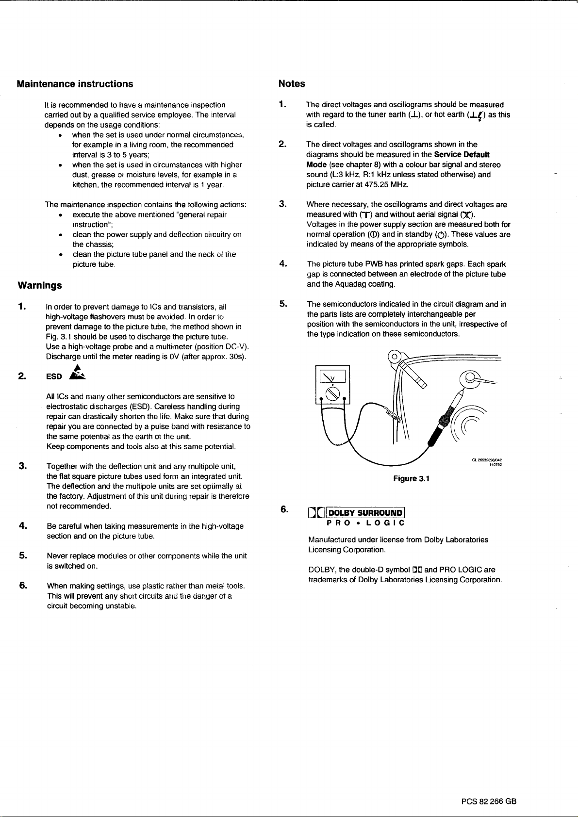
Fig. 3.1
Use a
Discharge
ESD IÈs.
2.
prevent
damage
should
high-voltage
until
l
damage to
to the
be used to discharge the
probe
meteÍ reading is
the
lcs
be ave,ided.
picture
tube, the method
and a multimeter
The interval
normal
circumstances,
for
exanrple
year.
1
is
"general
deflection circuitry
and the neck
and transistors, all
0V
In
order 1o
picture
(position
(afier
repair
oÍ
shon'n
tube.
approx. 30s).
in a
actions:
on
the
in
DC-V)
The diÍect voltages and oscillograms should
1.
with regard to the tuner earth
is
called.
The direct voltages and
2.
diagrams
(see
Mode
(L:3
sound
picture
carrier at
WheÍe necessary, the
3.
measured with
Voltages in the
normal operation
indicated
picture
The
4.
gap
is
connected between an electrode oÍ the
and the Aquadag coating.
The
5.
semiconductors
parts
the
position
the type
should be
chapter 8)
kHz, R:1 kHz unless
means
by
tube PWB has
lists
are completely
with the semiconductors
indication
oscillograms
measured in the
with
475.25
MHz.
oscillograms
(''ll-)
power
without aerial signal
and
supply section
(@)
in standby
and
of the appropriate symbols.
indicated in
these semiconductors.
on
(J),
hot
or
earth
shown
Service
a colour bar signal
otherwise)
stated
and direct voltages
are measured
(O).
These values
printed
interchangeable
gaps.
spark
circuit
the
in
unit, inespective
the
diagram and in
be
measured
(I{)
in
the
DeÍault
and
([).
Each
picture
per
as tnis
stereo
and
are
both Íor
are
spark
tube
oÍ
All lCs and
electrostatic discharges
repair
repair
the
Keep components
Together with the
3.
the flat
The deÍlection and the multipole units
the
not recommended.
Be
4.
section and on the
Never replace
5.
is
switched on.
When making
6.
This will
circuit becoming unstable.
nrarry
other semiconductors are sensitive to
can drastically shorten the
you
are
connected by a
potential
same
square
Íactory. Adiustmeni
careful
prevent
as the earth ot
and
deÍlection unit ancj any multipoie
picture
when
taking
picture
mocjules or otheÍ components
settings,
any
(ESD).
Careless handling during
liÍe.
Make sure that during
pulse
band
the
unit.
tools
tubes used
of this unit during repair
measurements in
use
short
at this
also
tube.
plastic
circuiis and tire ciangei
same
forrn
an integrated unit.
aíe set opiimally
ratheÍ than metal tools.
with resistance
potential
unil,
ai
is thereÍore
high-voltage
the
while the unit
oÍ a
to
Figure
3.1
6.
DCtpoLBY
PRO o LOGIC
ManuÍactured
l-icensing
DOLB'/,
trademarks oÍ
sunnounol
license from
under
Corporation.
the
double-D symbol
Dolby Laboratories
Dolbv Laboratories
PRO
and
D!
Licensing Corporation.
LOGIC are
PCS
82
266 GB
Page 5
4.
Mechanical
The
MD1 .2E
executions.
4.1
Styling
(also
Removing
1.
2. The
3. The
with top
applicable Íor
the
First
all screws on the rear
.
4
Screws are located
.
2 Screws
corners oÍ
.
4
Screws are
with the Euroconnectors
rear cover is
between
2
clicks
loosening
driver),
the rear cover
cover
connectoÍs
following
the
click connection
plate.
Process position
chassis has
controland
Íear
cover
located
are
rear
the
Íixed
now held
the
cabinet and the
at the left, 2 at
all clicks
plate
way:
on
and
aerial input
remove
(by
the
at the bottom
instructions
two
different
MD1.1E
at each
at the left
cover.
at the 4
the right
releasing
can
l/O
the
mechanical
side
inpuVoutput
Widescreen)
cover have
and aerial input.
position
in
rear
be removed.
panel
can be removed
screw in
to be
corner of the
and right bottom
corners
oÍ the l/O
by 6 clicks
cover. There
and 2
at the top. After
them with
with
the Euro-
the middle, release
and lift
removed.
cabinet.
are
a screw-
in the
the cover
panel
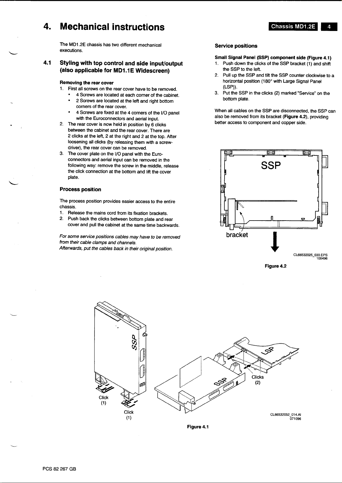
Service
Small
1 . Push
2. Pull
positions
(SSP)
Panel
Signal
down the
the SSP to the lefi.
up the
horizontal
clicks oÍ the SSP bracket (1)
SSP and
position (180'with
tilt
(LsP)).
3. Put the
bottom
When
all cables on the
also be removed from
better access to component
SSP
plate.
in
the clicks
its bracket
SSP
component side
the SSP counter
Large
Signal
marked
(Figure
"Sewice"
4.2),
(2)
are disconnected,
and copper side.
(Figure
4.1)
and
shift
clockwise
Panel
on the
the
SSP can
providing
to a
process
The
chassis.
1.
Release
2.
Push
cover and
For
some
from
AÍterwards, put
their
back
service
cable
the mains cord
position provides
the
clicks between
pull
the
cabinet
positions
clamps and
the cables
easier
Írom
at the same
cables
channets.
in
back
access
its Íixation
plate
bottom
time backwards.
may have
their original
to the entire
brackets.
rear
and
removed
to be
position.
bracket
PCS
82 267
GB
Click
(1)
Figure 4.1
_014.41
071096
Page 6
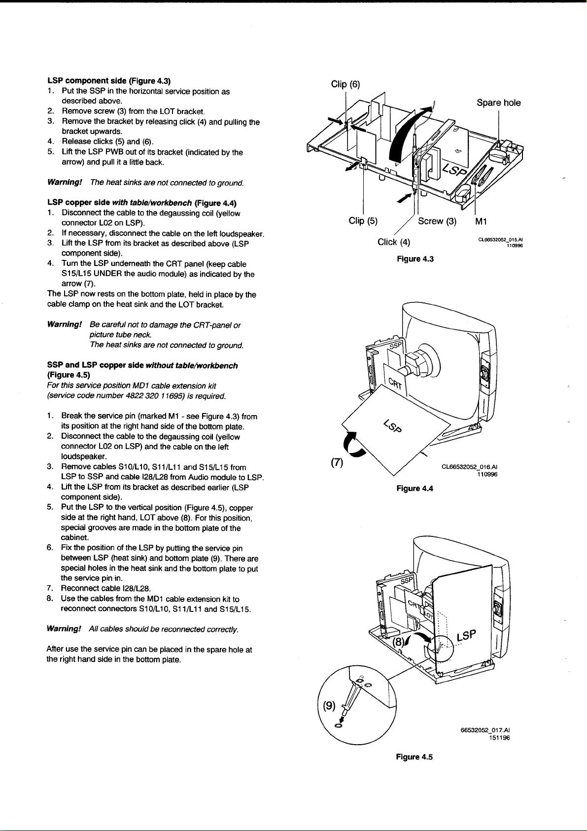
LSP
component
1.
Put the
described
2.
Remove screw
SSP
above.
(Figure
side
in
the horizontal
(3)
from
3. Remove the bracket
bracket upwards.
4. Release
5. Lift
the LSP PWB
arrow) and
clicks
pull
(5)
it
a little
and
out
the LOT
releasing
by
(6).
its
of
back.
4.3)
service
bracket.
bracket
position
(4)
click
(indicated
and
as
pulling
by the
the
Clip
(6)
Warning!
LSP
1.
The heat
copper
side
Disconnect the
connector L02 on
2.
lÍ necessary,
3. Lift
component
4. Turn
515/L15
arrow
the
disconnect
LSP
Írom its
side).
the LSP undemeath
UNDER
(7).
The LSP now rests
cable clamp
Warning!
the heat
on
Be careful
picture
The heat
SSP and LSP
(Figure
For
this seruice
(service
1.
Break the
its
2. Disconneqt
copper si]de without
4.5)
position
code number 4822
service
position
the right
at
the cable
connector L02
loudspeaker.
Remove
3.
LSP
4.
Lift the
component
Put
5.
cables
to SSP and cable l28lL28
lrom
LSP
side).
the LSP to the
side at the right hand,
grooves
special
cabinet.
position
Fix
6.
the
between LSP
special holes in the
the
7.
Reconnectcable
8.
Use
reconnect
pin
service
the
cables Írom the
connectors
sinks arc not
x/ith
table/workbencá (Figure
cable to
connected
the degaussing
LSP).
the cable
bracket
as described
the
the
on the
sink
not to
CRT
audio module)
plate,
bottom
and the LOT bracket.
damage the
tube neck.
sinks
are not
connected to
MDl
cable
extension kit
320 11695)
pin (marked
to the
on LSP)
51 0/L10,
hand
side
degaussing
and the
51 1/L1 1
M't
cable on the left
Írom
its
bracket as
vertical
LOT
described
position
above
are made in the
oÍ the LSP
(heat
sink) and
heat
putting
by
bottom
sink and the
in.
128/128.
MD1
cable extension
S1 0/L1 0,
S1
ground.
to
4.4)
(yellow
coil
on the left loudspeaker.
(LSp
above
panel (keep
as indicated
held in
CRT-panel
cable
place
by the
by the
or
ground.
tabte/workbench
is required.
-
see Figure 4.3)
oÍ the bottom
coil
and 51
5/L1 5
Audio module
earlier
(Figure
(8).
bottom
4.5),
For this
plate
the service
ptate
(9).
bottom
ptate.
(yellow
Írom
(LSP
copper
position,
of the
pin
There
plate
from
to
to
kit to
1
1
and 51
/L1
S/Li S.
LSp.
are
put
Click
(4)
Figure 4.3
Figure 4.4
c166532052_01
5.Al
1 10996
Warning! All cables
After
use the service
the right hand
side in the
should
pin
can
bottom
be reconnected
placed
be
in the
plate.
correctly.
spare hole
at
665320s2 017.41
Figure 4.5
Page 7

Mechanical
instructions
Accessing the module with mains switch,
receiver
1. Cut
2.
3. To
4.
Afterwards
(10).
4.2
Styling
control)
Removing
1.
Fot
írom their cable clamps and channels.
cables back
(Fig.4.6)
the tie rap
bottom side
bottom corner
space to handle the mains
Remove
pulling
and
get
be
can
The mains
with
First
all screws on the
.
6 Screws are located at the
.
2 Screws
the rear cover.
.
3 Screws
cover
some service
of the degaussing
(10).
Remove the
Írom
Íixation bracket
its
red mains
the
it backwards
more
movement
pushed
panel
the
degaussing coil should
side control and
ttre rear
aÍe
are located
plate
positions
in
their original
pànel
space, the
pulled
or
can now be
cover
rear
located at the
of the
UO
cables
LED
coil at the left hand
degaussing coil in the left
(1
1)
module.
bracket by
(12).
upwards
removed.
side
cover
just
above,
connections.
may
position.
lifting
left top of the cabinet
(13).
retied at
be
inpuVoutput
have
to
comers oÍ the cabinet.
right
left and
under and left oÍ the
haveto be removed
Aftenttards,
RC5
and
get
to
more
the end
position
(no
be removed.
bottom oÍ
put
the
top
(10)
(1
1)
(12)
Figure 4.6
66532052_01 8.Al
071096
Process
The
chassis
1.
2. When the clicks
Service
SSP copper and component side,
(Figure
'1
. Release the
2. Lift the SSP a little and turn
Service
1.
2.
3.
position
process position provides
during the
The chassis
fixed in the bottom
pushed
pulled
positions
4.7)
LSP.
(16)
180"
provides
This
SSP and also allows
position
Disconnect the cable
connector L02 on the
the
Lifi
backwards
Turn the entire chassis around the CRT
The
chassis rests
LSP backwards.
service
can be
between
back, the chassis and
backwards.
click construction
Írom the LSP.
better access
with table/workbench
from
chassis
(17).
easier
posltions.
pulled
lifted,
plate.
bottom
it to an angle oÍ
to the
for the removal
the
degaussing
to
LSP).
the bottom
the SSP
on
access to the entire
(t
Íorward
plate
the bottom
module servicing
(14)
clmponent
plate
with the
Scm) and
rear cover are
plate
between the SSP and
135'
oÍ modules.
(Fig.
4.8)
(yellow
coil
pull
and
panel (18).
copper side of
can be
(15)
or
side oÍ the
it
the
(14)
Figure
4.7
66532052_01 9.Al
250996
Warnlng!
careful
tube
not
neck.
Be
picture
The heat sinks
to damage
not
are
connected to
the CRT-panel
ground.
or
FiguÍe 4.8
Page 8
position
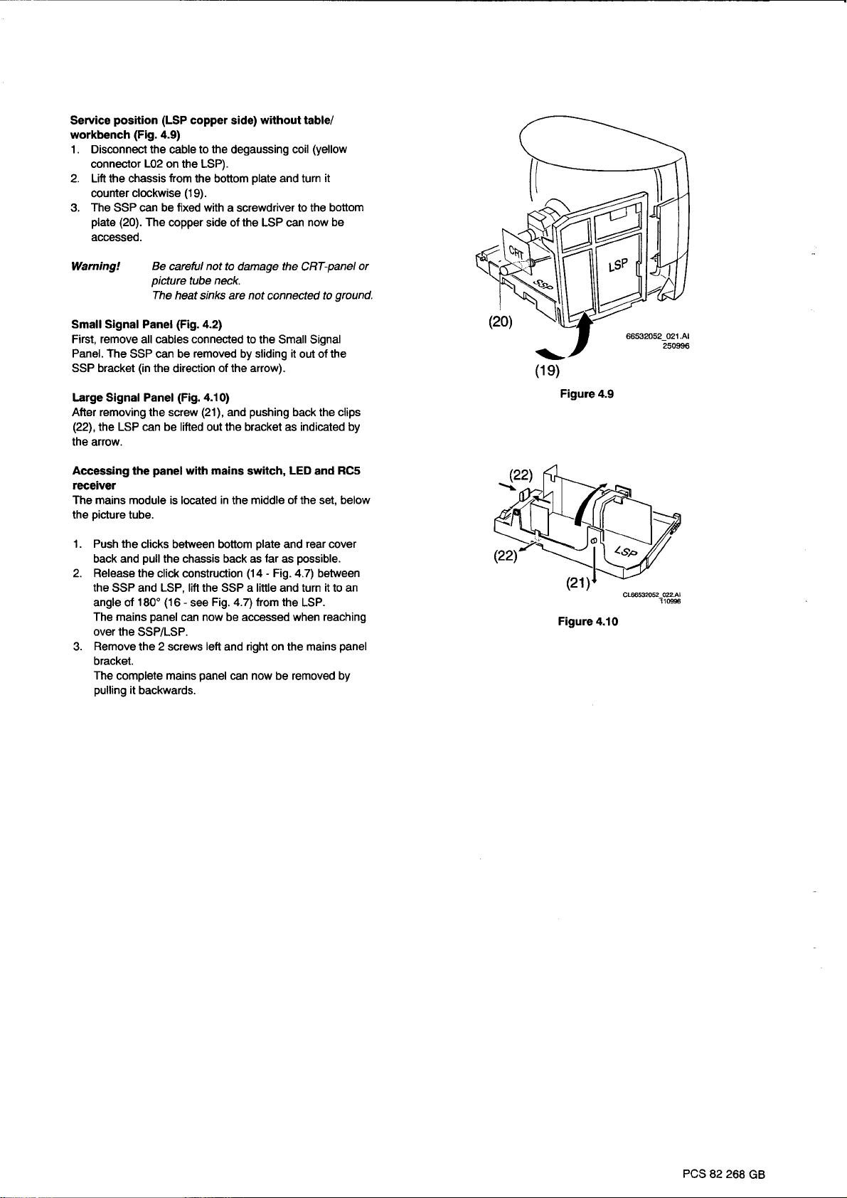
Service
workbench
1.
Disconnect
connector
2. Lift the chassis
counter
(LSP
(Fig.4.9)
the
cable
L02
on the LSP).
Írom
clockwise
copper
to the
the bottom
(1
9).
3. The SSP can be Íixed with a
plate (20).
The
copper side ofthe LSP can
accessed.
without table/
side)
degaussing
plate
and turn
screwdriver
(yellow
coil
it
to the bottom
now be
Waming!
Be
picture
The
Small Signal Panel
First, remove
Panel. The
bracket
SSP
cables connected
all
SSP can be
(in
the
Large Signal Panel
After removing the
(22),
the LSP can be lifted out the bracket as indicated by
the
arrow.
Accessing
the
panel
notto
careful
tube
damage the
neck.
heat sinks are not
(Fig.4.2)
removed
direction
by sliding
of the arrow).
(Fig.4.10)
(21),
with
and
mains
screw
cannected
to the Small Signal
it
pushing
back the clips
LED
switch,
ÍeceiveÍ
The mains module
picture
the
1. Push the
back and
2. Release the
the
SSP and LSP, lift the SSP a little and turn it to an
angle oÍ
The mains
over
the SSP/LSP.
Remove
3.
is located
tube.
clicks between bottom
pull
the chassis back as
click constÍuction
(16
180'
panel
the 2 screws
in
-
Fig. 4.7)lrom the
see
now
can
be accessed when
left
and right on the mains
middle oÍ the set. below
the
plate
and
Íar
as
-
(14
Fig.4.7)
bracket.
The complete mains
pulling
it
backwards.
panel
can now be removed by
CRT-panel
ground.
to
out of the
RCS
and
rear
cover
possible.
between
LSP.
reaching
panel
or
Figure 4.9
cffi262 02.A1
-i1ffi
Figure 4.10
PCS
82 268
cB
Page 9

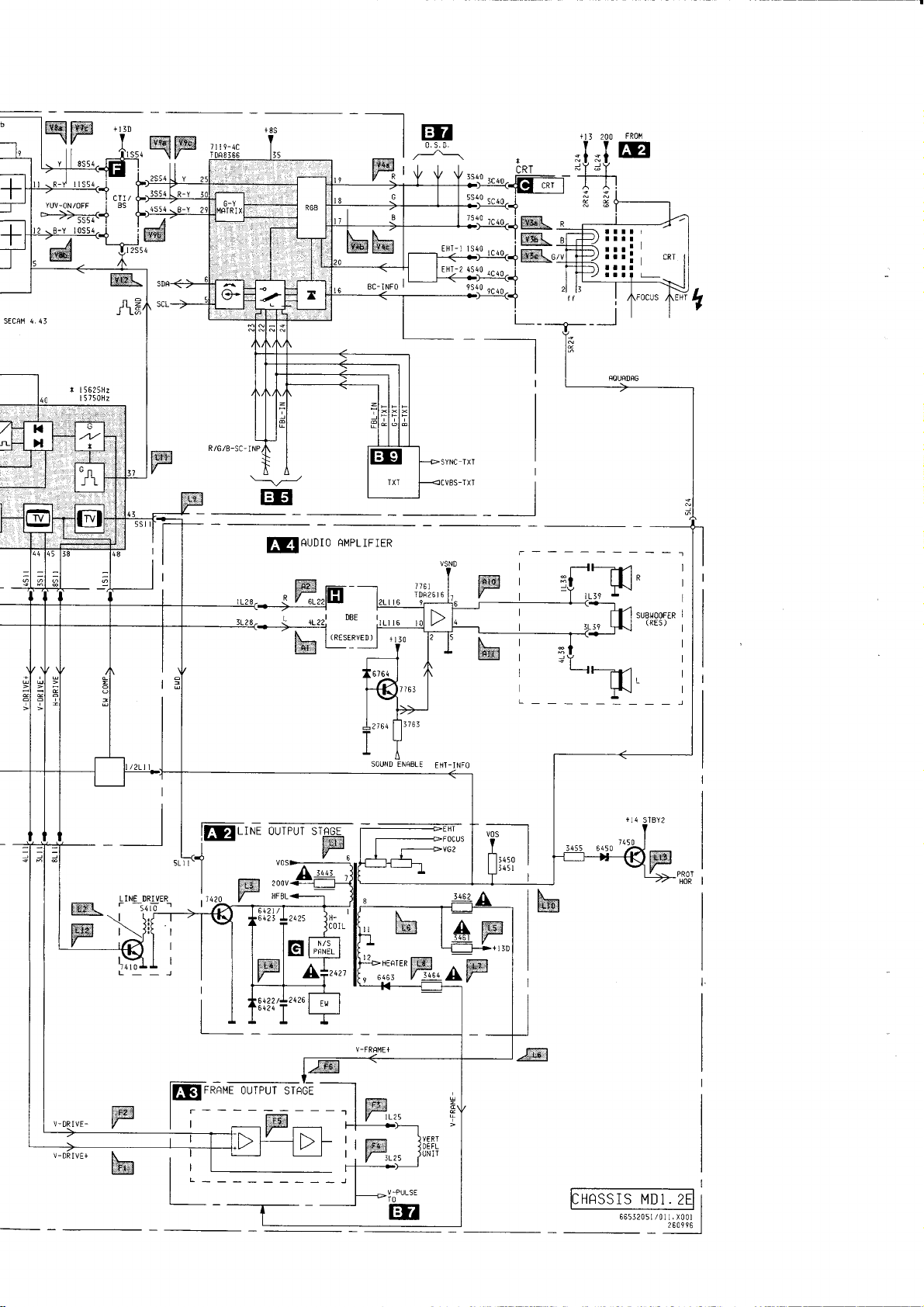
5.B|ockdiagram/B|ockscha|tbi|d/Schéma.bloc@r
7l I 9-4ê
PANEL
I
Titr
SÍEREO
SND(L /R
)-SC2-OUTP
FBL-PRESENI
STATUS
(FOR
IF
STEREO OSS
NICêM
,
I
*rry
)
i* .,r*ro
x
L
os, o'*
t1'rttfïr%,htit
cv8s-sc
cvBs-sc
| - INP
2-0uT
PÊL/NTSC
*Tt
PHASE-COMP
OR SECAM
ryF
4. {3
t
i
l_
SOUND(L/R) HEADP-OUÏP
t
1392/1394
!
mr-lmalrcto
puDro
(r
/R)
uoourE]
!l
: I
tl
6504
3ND(L/R )
/R
-SC
I'I NP
-5C2lÊR-t
)
hm,/qt?&]
-
v
m
v
73so/r3sr
f--;1
A
::i;i:?\,'" F
,6|$ffii!$i,
s
I
PROT
t@
tr
,Ó
È
Ift-ltl
SND(L/R)-scr-ouTp
/R)-SC2-0UÍP
SELECT
2
SND(L/R
)-CL OUTP
ut
rrtoe*
ffi
E
Y
PCS
L-
82
269
Page 10
--l
rytr+
ffii{r
Íts
t I 5525H2
I 5750H2
,ryffi
ffi
EEI
EEAUDIO
I
ÍEA .
|
V-*
AMPLIFIER
EHT-2
4540
iiiiicRT
I
I
I
I
I
I
I
DBE
(RESERVED
)
ïï:'"&aP
v-DRIvÊ+
WT
IÍGIrnnur
r::ï | -----
lËr I l----rar---l
f
t\
lr.r-
I tlP-
--r\rt
OUïPUÏ
STAGE
|:H
|
V'PULSE
TO
EA
HÊSSIS
MD
66532051 /01
1
]
.
X00
t
Page 11
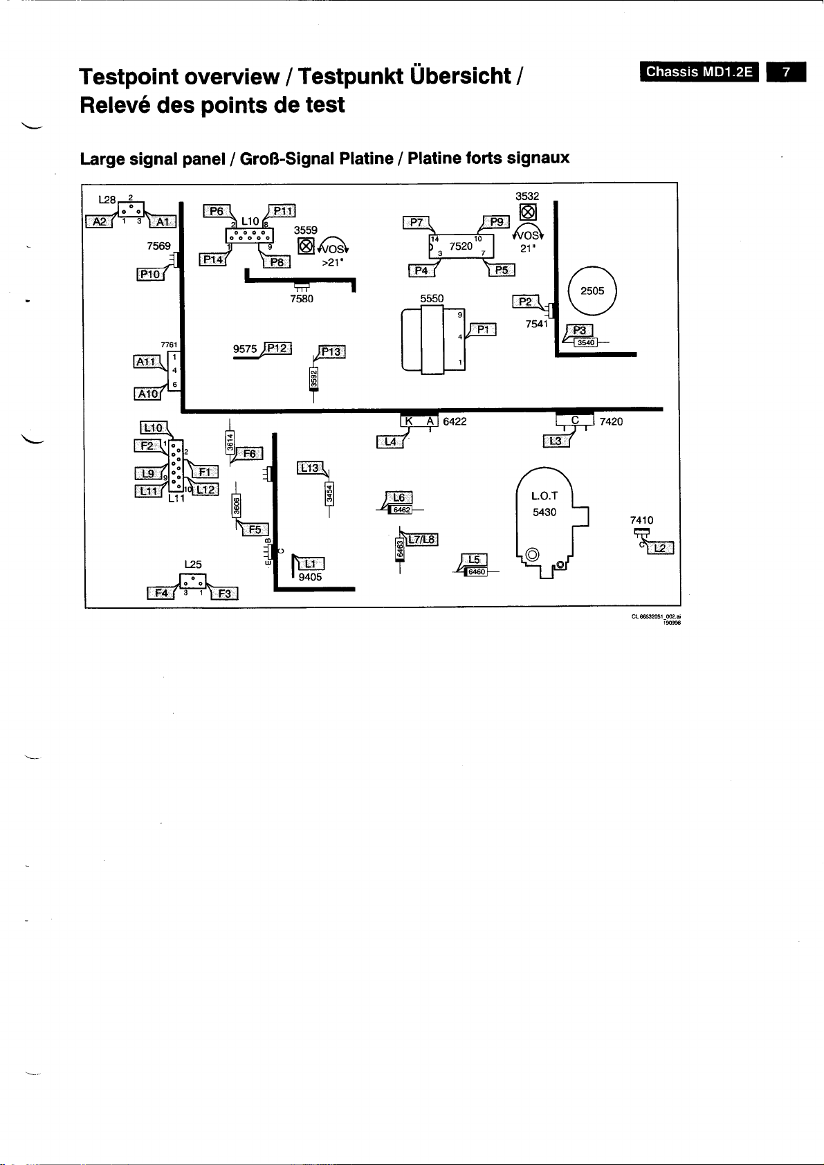
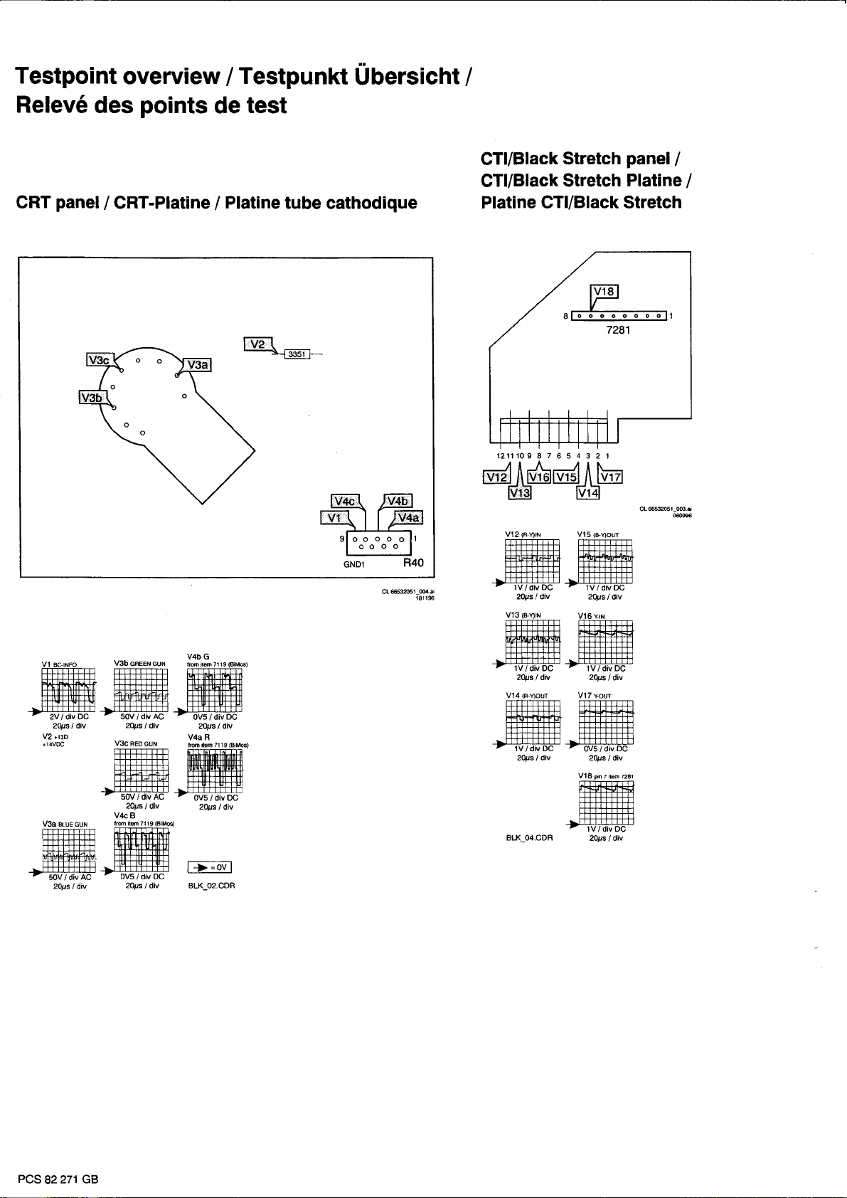
Testpoint overview
/
Testpunkt
Ubersicht
/
@z
Relevé
l-arge
des
signal
points
panel
/
test
de
GroB-Signal
Platine
Platine
/
Íorts
signaux
c1ffi261-@.d
1$S
Page 12
z
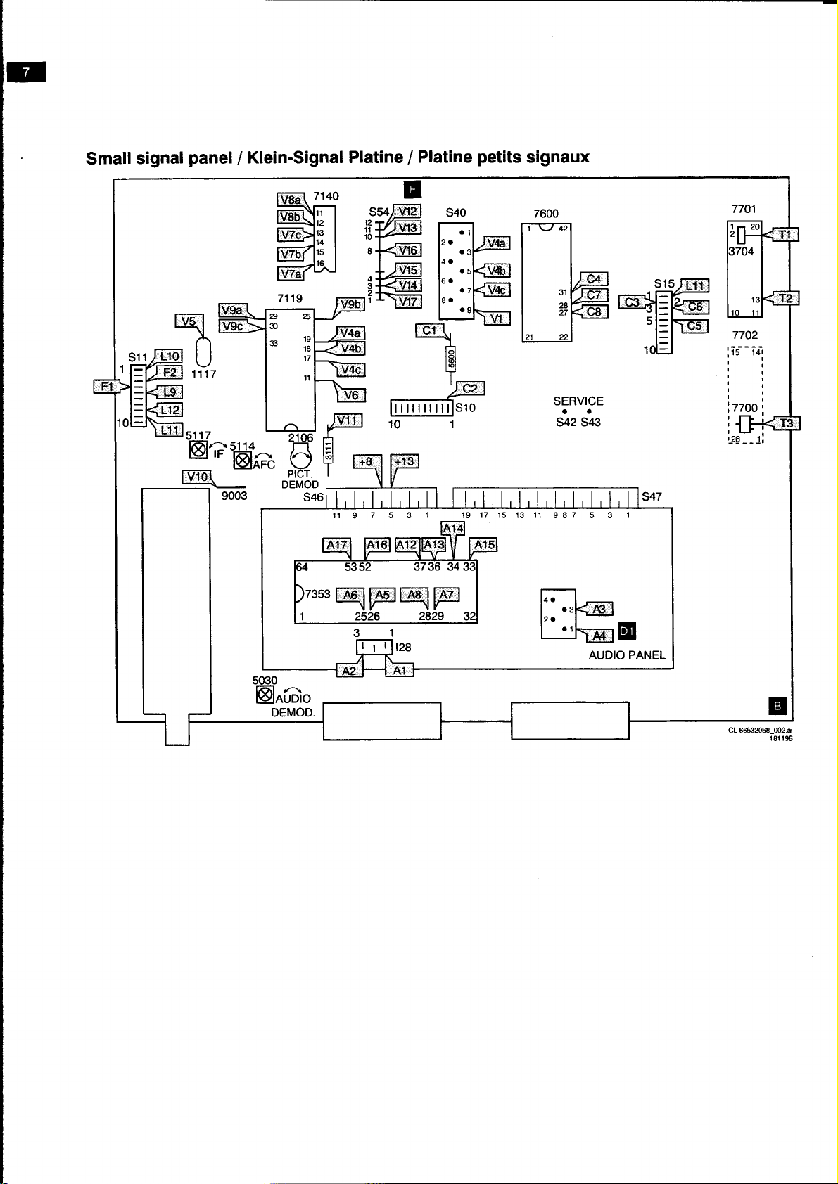
Small
s11
signal
panel
Klein-Signal
/
a6
O
to
33
;;
17
11
Platine
Platine
/
petits
signaux
7600
\Jt
42
1
31
2A
27
:C8
SERVICE
aa
s42 s43
c4
7701
7702
ï4-'
:ïi
It
It
It
It
ll
y
i77oo
ifii
V9--1.
qtr
2526
E
CL 66532068_002.ai
181196
Page 13

Testp
Relev
A1 ND6-L,3KHZ Al0 Adb ilp. od C'l
(wrlmkrinsed)
FTffi
TFFEFFEL*LI 'ítrtt'f.'r'r
mnÍrirrÍf,Il|sr
m '' w
ffil.++w
F#r#tfH ffiMl-*td/i
TrrrTrT-trTn TrtrrrrrT-rfl
div
50mV
/
O.sns /
A2ruDo-B-iffiz
(wilm€MiEs6€O 3ft2r4(id.wrlm)
IKH:igh(iffi.dm€)
ffi
r-rT\1-TÍT1\TT1
0V2
AC
div
div
AC
/
O.l ms / div
All ^dbilp.od F3vERTrcaL
+5$NDBY
(Ên.2itm7&o) F2voRvE- L5+13D
Mc
czrclreogr
-$ï:i:]-ffi
CjvpuLSÊ OEFLECTToN(LV-)
ffi f;fffiffi Tffïffi
ffi
H#++H#
í)mv/divAc
O.Sms/div
A3 sNoL-HmPH-ouT A1 2
Hp rÉ.wrom,
{3G2,
"hïïiffi
ffi-ffi-ffi ffi
H+ËH+W HSH++ffi
ov2/dvAc
o.zms/div
pin
37 n€m
(S'-OUT-1,
3KHz)
ïfiïïPft
ovs/divDc SV/divDC!
sms/div sms/div sms/div
73$ F4 vEtrrsl V6
g
-
(8MHzffiiltu4
+ffi ffifii ffi
ffi
ffi
ffi
H{++fi+#
OEÈECTTON
, HrJ#tt+r
-ryii"tê-
(Lvr)
14wm
'*ïJ:**.
P4pingirmuszo
ffi
ffi
;;-**
LgEwo
ffi
L10 S-COMP P6 vOS
ffi
P5íh7íêm7m
ffi
ffififrffi
Fffffl-l-Frï1
'ád**vroiurc
1oírs/div
*"Íl:,119"?" rllrrr|T
Pl2*28
souNo-suPPLy
Íi:::,,.,."
*fr:Ïn'"':*.rmffi
P14
tri:,?":'
!""ïÁ.ó"o'-ffiffi.ffi
pin
its zO1
T1
2
V4c B
hmilma1g(aik)
ilr6qrilfin
ffi-ffi ffi
Vsaa3MH2qFd
.
ffi
ffiffi
2omvfd'dDc ï5viáil#
62-5gs/div 2q[s/div
CWS-TEFR$T
(Pd]
-T];ff
ffiffiHfivtrfrn-ffi'ffi ffiffi-ffiffi
ffi)trffiffiffiffi
O.2ms/div
A4sNDR-HmpH,oUT
(rffi,HPiEdumê,
rE.woFRn]
r-rJ-+-r-r+r-r.r-1 ++4r-+-r-r-r-r
ffi
ffiffi>'ïuF,Jï'"''
O.2ms/div
A5
Írn6Mre$
(tiP-L
oW - 3KHz) (gz-óur-r.
ffiffiffi::* ffi8:Y3:
ffi-ffi-ffffi,$
o.2rc/div
m.'Jtïr':ïá1ï
ffi ffi
ffi ffi''$Frrrflrrl
lVrH-+\,í-H +t++rffi.j
Hffiffi
o.2ms/div
pn
A7
ê nsm
(LNOSffiËF-1,
liïi'fifi,ï,]
ffi
ryfrWW
ffi
o.2ms/div
A8Íhanem73s
(LOUSffiRA,
,,(u*"*6)iarzat..irlt-ETrr
ffiffi
ffi
O.2ms / div
o.zmsidiv 62.5ns/div sms/div
A13Írn$bm73s
(sc1-oUT-R,1KHz)
trrtrrFrrrrr'l
CssoA L F5b$oídm76o2
ll. Il li't
[]ju_lH
ffi-ffirffiffiffiffififfi-ffiffi
1V
div
/
Z)ms/div
o.2ms/div
pn3ail€m73s
414
sxnr)
o.2ms/div
êHS,},ïï[,fi"
20ms / div
ScL F6 VFMME*
C6
2oms/div
:"t;l;:g'Sg
ryiïiffi ffi
lffit Hi*tN1f6
uffi)ffi
73s
o.2ms/div
lq/s/div
C8pin2zils7ru
ffi
ffi ffi H+trilffi"Tliffïfrf ffiflfiffi-ffi ffi
Hffi
êl?.ïÍ.li?"*e,ffiïg
Ar;;;;;r"*
lscr-ir-a,rxx.,
È6. $ud ON)
sms/div
Fl vDRG*m L4
.Tf[mfi
Fïïffi
%ffi+ffi>Hm
0-2ms / div sms
-tftfEttr]::m
+H-Ftttï ttutffi-rh
DC
ffi)tr#)ffiffi
1oms/div
*ï.r';9tr-ffi
L26róíM74,0 Lr3Bc.pBm
H+Hd
lQt/s/div
L3ar@rilem74a P2ddní€m7Ím1
ffi
Fu1l+tffi
+ffi
lq/s/div
ffi
W-ffiÉ,*r-"
div
/
5ms /
div
sms/div
Lít SAND
Í-TTr-rfrrl-T-l t.|-trrTT'arÍTr [-fffl_Í-T_ff|l roI-rn-fr ro
1ops/div
L12 H-oR
2orjs/div
w2rc
plpnilms$o
ËErl|T-ili,;FrilTtT]Tl
ffi ffitilïn
-qffi
tqss/div
P3 dhde ím 6í5
fi:ffi
q:í##
gls
P7pin14rem73o
(D ry5rc
"tthhbftf++r
o.1s/div 0.59s/div
_
vE
+rySÍaNoW (r=oN)
PB
pspinloibmTs
offi
ffiffi +ffifififfirffi ffi
H-r-rfr1.j
+ffi'ffi
lqgs/div
Pgphlon*7ffi
)ffi
o.1s/div 2qss/div
Pto+Es V4bG
(O
SW
[ou*
ó*
/ div
,q|ffiffiffiffi
2qgs/div
T2pin1orm77o1
frurel
H-H # H+#+#
T3 sYNC-w
sq/s/div
v1
Es.]rrc
ffffi ffi
t1ïïfr*l
2qgs/div
V,fa R
Miêm7119(sM6)
ffi
1q6/div
V6cvBs-TERffiaT
(s*m)
ffi
1ops/div sqis/div
Xlli",J,?i;,
ft'.-ïhï
ffiffi
lqps/div
V7c Y ouT
(Ítnr3im714o) V1z(Ê-Y)LL
ffi--I-Í-Tifr-rr
r-l$ifl11u1l
ffi
tom
7119
ísm
ffi rffi ffi
ffiffi ffi
+riv,,o-"o'#
2q!s / div
ffi
lqgs/div
VgaF-Y
(pin
(BMc)
r 1 n6m 7l{)
-dEffi)"ffi
2Ws I div
V8b 8-Y
(pin12
ilm714)
FEfn"TfFFtr
!!!(B-\4oW
-T[rrnTr
ffifu
V9a(B-Y)OUT
trffi
ïïFïFïl-l -
vgb YOUT
rrr--Ttm Ftr;r-ifrn
2qgs/div 2qgs/div
Vgc(R-Y)oW V17Y-ouÍ
-",->ffi
vll NEsNprys
E'rrïrrtr
fï'Íïfi-rll-
-
2qgs/div
ffi
2qss/div
(8-ïlN
v13
20t1s / div
Vl5€'\4OUr
ffi
ffi
H1+H++H
+-fV;a;Oe-
2qts/div
yrN
V16
-TTrfrFÏ
+r#
f+=ovl
BLK Oí.CDR
CRT
V1 Bc-rNF(
ffi
Hl-tsHtl
Ffitfl-1-ttl
rffï1-t't
)=ffi
V2 +13o
+1.Vrc
pa
2OUs
I
PCS
82 270
PCS
82
27
Page 14
Testpoint
overview
Testpunkt
/
Ubersicht
/
Relevé
CRT
Vl rc-rNFo
ffi+Fffi
HÁHS,{+rh,l.H
ffi1-fffttfiitiÍl
ilqIqTTF]
>qffi
V2 +t3D
4vrc
+1
ffim'
IflFi'FFffiS+
des
panel/
2qgs / div
'>}#+'ffi
2qls / div
points
de
test
CRT-Platine / Platine tube
V3b
GREflGUN
frfftfrl+ï
l..]...]..]...]...l..]'."1+
titrfft+r
FliJ+FUfft{
n-TTn-TT--l-1
)-Siftr'ïd
2ots
V3c RED
ffi
-ï-t-TTn-ï-TF
uïtrEEtmf
Í..]...l:::]l..]...|::]].]...m
n-Í-rft-n-n
''.'ofrbi;ïd'
2ogs / div
V4c B
IlHÏfi1Uï1
2qgs
ffiffiffim'
ffi
TtT|TgtTgl
+5ffi
div
/
GUN
/ div BLK-o2.CDR
2qgs / div
V4a R
MM71r9(Bft)
W
ffifmEt
+ffi
20us
l>=ovl
div
/
cathodique
cLffiru1_@.ai
1811S
CTUBlaek
CTI/Black
Platine
1211109 8 7 6 5 4 3 2 1
Stretch
Stretch
CTI/Black Stretch
dAtrd/\b
Ed Éa
V12
G-Y)|N
ffiEffi
ffi$ïïFtrï1
ffiffi
>'iiititb"
2ogs/div 2qps/div
(B.Y)|N
V13
ifift[T-m
ffiffi
tfft-ft-l-f-t1
>'ïiii*tb"
20ps / div 2qgs
V'14
íR-souÍ
lTfrfl_Tff|r
r.|M
ffiirHrffiH rir-ffi
ET]ffiTI]]] EIT]IIE]T
L|!n -a*_l
>'ï#i*ib" >-btÈïàibÉ
2qps / div 2Ws I div
BLK_O4.CDR
(B.tour
V15
Frtrtlriltf
+'5v#JÈ#
yrN
V16
rrnTTTFm
Ffl-Fffn-ff1
-'!l
+'ïii#iË
V17 Y-our
gErrrrT-n
LIJ+.qJaJJ
div
/
panel
/
Platine
cLwost_m.d
ffi
/
PCS
82
271 GB
Page 15
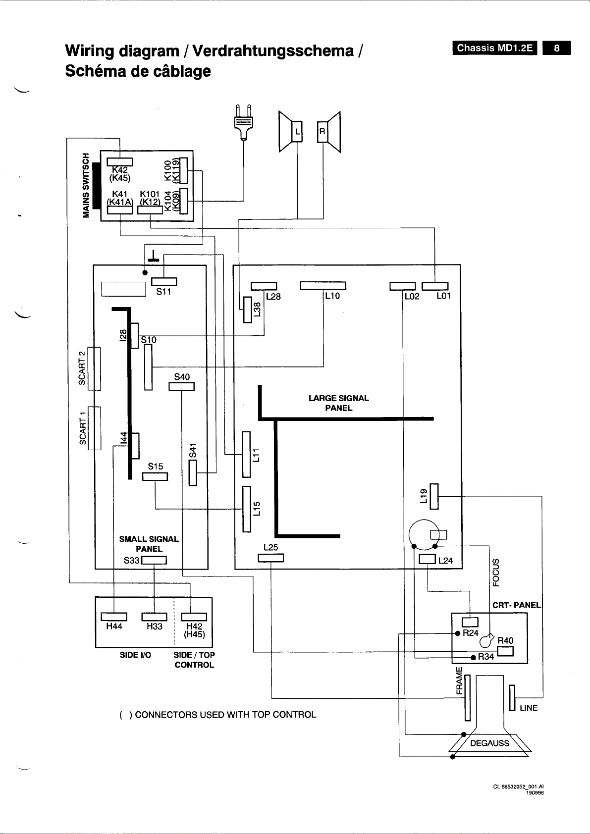
Wiring
diagram
Verdrahtungsschema
/
/
@r
Schéma
de
riiiSl
í11^, lÍ.1.E
T--__lï"
càblage
v
I
SMALL SIGNAL
PANEL
SIDE I/O SIDE / TOP
CONTROL
(
CoNNECïORS USED WrrH
)
TOP CONTROL
U)
l
O
lL
CRT.
cL 66532052_001.41
190996
Page 16

6.
Service
Modes,
DST, Error
messages,
Protections,
Faultfinding and
following
In this chapter
6.1
6.2
6.3
6.4 Protections
6.5
6.1 Test
The MD1 chassis
printing.
blocks:
A1-42-43, etc.: Test
*
* C1-C2-C3,
* F1-F2-F3, etc.:
L1-L2-L3, etc.:
*
P1-P2-P3, etc.: Test
*
* T1-T2-T3, etc.: Test
V'l-V2-V3, etc.:
*
6.2 Service
For
easy
RC7150
TV
sets,
also called
number of
Installation Íeatures Íor the dealer
6.2.1
The dealer
presets,
with
the
points
Test
Service Modes and Dealer
codes
Error
finding
Fault
points
is
These test
etc.: Test
modes
installation
is introduced. The
including
all set of
Dealer Service Tool
the DST
can use the RC7150 for
Tv-settings,
Repair tips
paragraphs
"blinking
and
repair
and
equipped
points
with
are reÍerring to the
points
circuitry
points
points
Test
frame output circuitry
Test
ooints
output circuitry
points
point
points
Test
circuitry
and Dealer Service
and diagnosis
RC7150 can be used
the MD1 chassis. The RC7150 is
(RC7150)
is
Dish
are included:
Tool
Service
procedure
LED"
tips
points
test
for the audio
for
control circuitry
the
frame drive and
for the
Íor the line drive and line
power
for the
for the teletelc circuitry
Íor
video
the
the
dealer
DST. The ordering
or
4€,22 218 21232.
programming
settings.
(DST)
in the service
functional
processing
supply
processing
(DST)
Tool
remote
control
for
new
all
Tv-set
the
Exiting the SDM:
-
Switch
cleared).
Note: When
The
SDM
microprocessor controlled
-
For recognition of the SDM
the screen.
oÍ
-
Tuning
Nicam L), PAL on other
-
Volume level
level).
-
Auto switch off
switched off
for 15 minutes).
-
Sleep
-
All other controls
-
When
procedure (See
error buífer,
to the value of
This function
plcture.
or
Alignment Mode
Seruice
6.2.2.2
Entering
-
By transmitting
Dealer Service
normal operation
-
pressing
By
keyboard simultaneously
the
to stand-by
set
the set
immediately
again'
Íollowing
has the
475.25 MHz
at
is
set
picture
Other
timer is disabled.
the microprocessor supports the
SAM:
disabled
when no
operate
6.3) and an error code is
the LED
the last error code.
will
the
Tool
mode or
"MENU"
the
(the
error buffer
the mains
is in SDM,
to
also
"ALIGN'
power
the
set
the mains is switched on
when
pre-deÍined
tuning and linear functions:
"SER"
is displayed at the top
(Secam
on
Multi-France sets
sets).
(oÍ
25olo
the
maximum
sound settings are set to 5096.
and
(normally
video
will
blink
work when there is
(SAM)
(this
and':"
the set
(IDENT)
signal
normally.
the number of times, equai
command with the
works both while the set
in
the SDM).
key
when the set
is also
is
switched off
will enter to SDM
conditions
on
Íor
volume
is
automatically
was received
"blinking
present
no
the local
is in
SDM.
RC7150
while
all
(with
LED"
in the
soud
is in
10
Differenl
via a GFL or
to
the
DST-I
For
directions
program
tables can be
MD2 TV-set
(downloading
DST; see GFL or MD2 service manuals) or by the
(DST/PC
explanation
interf
ace; orderin g code 4822
of the installation
for use of
the
DST
chassis, download code 4 should be used).
Diagnose
6.2.2
The MD'|
DST RC7150.
and the Service
entered by
6.2.2.1 Service
Entering the SDM:
-
-
features
.2
sets can be
These
Default
short circuiting the
Defauft Mode
transmitting the
By
RC7150
By temporarily
Signal
Dealer
Panel.
for the servicer
put
are the Service Alignment
Mode
(SDM)
"DEFAULT'
Service
shorting
programmed
from the
into the DST
GFL
21 8 21 27
Íeatures
recommended
are
of the
DST, the
(For
in the two service modes
Mode
(SDM).
"seÍvice".pins
Tool.
pins
S42 and
can also
SDM
on the SSP.
command
S43 on the Small
with
the
or MD2
n.
the MD1
via the
(SAM)
be
Êxiting SAM:
-
Switch the set
Note: When the
ln the
SAM
screen:
-
Software
microprocessor
version identiÍication
versions in the Software Survey
Product Survey.
-
Error code buffer
-
Options
-
Alignment and
8.2.1, 8.3.1
to stand-bv.
mains
is in
Íhe sef
immediately when the
again.
the following
version
(see
and 8.3.2).
information is displayed on the
(the
software
in the
set
corresponds
(see
paragÍaph
geometry
power
is switched off while
the set will entet SDM
SAM,
is displayed. This software
paragraph
8.4).
information
mains is
version oÍ the
with
the software
published
as
6.3).
paragraph
(see
switched
on
in the
Page 17

Service Modes,
(1)
SoÍtware version
(21
Error
(3)
(4)
buffer
Options
Alignments
and
DST, Error
geometry
messages,
Example:
Errorcodeposition
Errorbuffer
c
afterenteing SDM
(2x) - pause
blink
.
after transmlfÍ,íng
(4x) - pause
blink
o
blink-pause-blink
.
nothing happens
transmrftlng
after
after transmltÍrÍng
-
blink
-
blink
1 2
2 4 1
(2x)
"DIAGNOSE
(4x)
"DIAGNOSE
"DIAGNOSE
3 4 5 6 7
0 0
2 OK
with the
with
3 OK'
4
with
OK'
0 0
DST
the DST
the DST
6.3
Figure
6.1
Error
codes
Ïhe
error code
last
time
the buffer
to right.
-
-
The last
The
error detected
error buffer will
1. exiting
remote
2. transmitting
the DST
-
By leaving
buffer is not reset.
Examples:
ERROR:
ERROR:
ERROR:
The
contents
through the
useful when
1. When
"blinking
there is
the SDM is
oÍ times,
The
LED will
times,
equal
2.
With the DST
made visible.
"DIAGNOSEx
The
LED will
now Íor
the error
Screen
Mode
and
buÍÍer
the
control
the SAM with
oÍ
the
Service
Alignment
(SAM)
"blinking
LED"
contains all errors detected
was
SAM with the
the
The
erased.
(actual)
reset in the Íollowing
be
commands
buffer is written Írom
is the error at the
"standby"
"DIAGNOSE
mains
the
switch,
command
procedure
since the
left side
cases:
on the
9 9 OK with
the error
000000: Noerrorcodedetected
3 0 0 0 0
0:
Error
code 3 is the last
and
only detected error
530000: ErrorcodeSfirstanderror
last
code 5
of the
erÍor bufier
equal to
stay
LED:
no
entered,
the value oÍ
off briefly and blink again the
can also be made visible
procedure.
picture.
There
the
the
to the value to the /ast
a// error
codes
in
While in SDM. transmit the
Ol( wherex is the
error
x ranges Írom 1,
(actual)
detected
This is
especially
two
are
methods:
LED will
blink the number
/asÍ error
code.
error code
the error buffer
command:
position
to
buffer
be made visible
(the
error) to 7
number
can be
in the
last
(the
Íirst
error)
operate in the
code
on
same
position
way
x.
as in
point
1,
but
left
Note!
lmportant!
Enor
code
Note
the set respons
lnterruption
lead to incorrect
Not
chassis support
and the DIAGNOSE
versions
procedure
it
that
all software
NOT
are MlZBAx-x.x
EÍor desoiption
may
take up
to a DIAGNOSE
of
the blinking
results.
versions
the blínking
99 command.
supporting
Bfinking
l€D,
to 7 seconds
contmand.
sequence may
of the MDl.2E
procedure
LED
Software
the
blinking LED
and Ml2COx-3.x.
Pgssble
deÍectve-
before
.
,
coÍnpgnents:
No error
0
BIMOS
(ID48366)
2 MSP3400/3410
erÍor
lzc
3
4 Wrong EEPROM 4x
5 EEPROM
defective
b Tuner errol
oÍ
7 TXT
Histogram Proc.
8
eÍror
9
error
10 WSSB module
error
11 Dolby
erÍor
detected
error
bus error
error 7x
processor
16:9
processor
1x
1c7119
(SSP)
2x
1c7353
(ssP)
3x All lzC-related
components
(SSP)
rc7685
5x 1c7685
6x
8x 1c7210
9x 1c7440
10x
11x
(SSP)
(ssP)
u1000
(ssP)
rc7702
(Íeserved)
(16x9
module)
tc7540
(WSSB
module)
rc7600
(Audio
module)
Table
6.1 Error
code
list
Page 18

Protections,
FaultÍinding
and
Repair
tips
Protections
6.4
In
6.4.1
the MD 1.2E
the
possible:
Protections
o
o
o
.
DeÍlection:
o
o
r
Soítware
o
.
o
Power
6.4.2
The
mode
r
r
o
o
ln hick-up
Pin 1
approximately
protection
hick-up
squeak is
6.4.3 Horizontahprotection
When
the voltage
conducting
is 0V7,
Via
the
switching
is
still
mode)
6.4.4
Ew-protectaon
generated
Overload
Undedoad
Over voltage
Under voltage
Horizontal
EW-Protection
Vertical
BIMOS
Set
there is no
SDA
Set is
restart.
No +SDb
standby via
power
Overload
Under load
Over voltage
Under voltage
the hold-circuitry
protection
protection
Protection
Protection
protection
lC71 19
can be
switched between
picture,
or SCL
switched
or +8Sc
supply
supply will
in
following
the
protection
mode
of 1C7520
2 seconds, immediately
is astivated.
mode.
When the
audible
the beam
across
and as soon
TS7450
will
mode
the set
present,
the set will
again.
deÍective
shorted
to
standby
protections
starts up
every 2
current
C2450 will
conduct, making PROT
of
(standby)
off and
(not
standby via
atgC
go
situations:
Íollowing
the
by
no OSD,
protections
power
--+
+
+
-+
-+
-+
-+
-+
standby
sound is
-+
standby line,
-+
line,
set tries to restart.
to a very
from
This
good
the
start circuit Íor
cycle is constantly
set is in hick-up
seconds.
becomes too
drop. D&50 will
as the voltage
power
the
on
Íor 21"
supply, the, set will stay
and
can only be reset by
via
the mains
switch
to standby
sets)
are
supply:
Hick
up mode
Hick up mode
Hick up mode
Hick
up mode
Supply
to standby
Supply
to standby
BIMOS
standby
(ErroÍ
code 1)
and ON, but
noise.
only
(Error
code 3)
tries
set
is
Set
switched to
audible hick-up
after that the
repeated in
mode
a short
high Íor a long
staÍt
drop across R34S6
high.
switch. lÍ the Íault
(protection
mode
to
period
in
The
EasVWest
the Easvwest
Note:
The current through
the LSP via
In
case oÍ a line
too high
rises.
to
and the voltage
When
conduct and
becomes HIGH.
high
(e.9.
when
switched
conduct
The
a
on with the mains
and EW-PROTECTION
East/West
cases:
1.
Bad contacts
.
bad contacts
r
bad contacts
.
bad contacts oÍ
2.
Bad
contacts
3. Shorted flyback
4.
Shorted S-correction
5. Bad solder
When
EW-protection
transistor
6.4.5
Vertical-protection
7420 may
The vertical
VERTICAL-PROTECïON
when
it is
the
interrupted,
mode.
functioning
BIMOS lC71
the BIMOS
In the BIMOS
oÍf the VDRIVE+
6.4.6
blanked.
line output
switch to
Software
The
It
Circuit breaker
stage will not work
hick-up
protection
software
continuously verifies
supply voltages
When
switch the
pÍotection
the
power
STANDBY line.
a squeaking sound.
protection
power
A cunent
is too high
part
precision
2
problem,
detects when
output
stage
through the
can be
in the line-deflectíon
the
EastArVest
resistors (R3483
the
easvwesÈcurrent
across resistors
the
voltage level
exceeds
STANDBY-SUPPLY
When the voltage
problem
line
ís
already
switch), D6zl81
protection
becomes
oÍ horizontal
deÍlection
of horizontal
oÍ linearity
S-correction
oÍflyback capacrtor
diode D6421
capacttoí C2427.
contacts in
output
has
also be
stage creates
line
the
been active, the line
defective.
pulses
correctly. These
19-4D
pin
on
37. When the
will
switch to BIMOS
STANDBY mode,
and VDRIVE-
'l463
may
and the
(under
mode
protection
pin
on
becomes
supply on
In
this situation
voltage
is
managed
presence
the
34 and the
active, the
and off continuously via
the current
with
TS7480
Easwest
caused by
is too
stage
a defective
circuitrv!
stage is measured
and
R3484).
becomes
R3483
and
0.6V, D6480
PROTECTION
across
C2480
is very
present
when
and D6,f82
is
activated very
active in the
Íast.
Íollowing
circuit:
deflection
corrector
coil
coil L542i
capacitoÍ
C2427
C2425.
D6423.
or
output stage.
output
at every flyback
pulses
are sensed
pulse
STANDBY
the BTMOS
while the
RGB outputs
be open. Probably,
power
supply will
protection).
by the microprocessor.
of the +5
activity oÍ
and
the l2C bus.
soÍtware will
the
power
supply
produces
through
high.
that
on
R3484
stans
the
set is
pulse
by
train is
switches
are
the
+8
the
The
EasVWest
standby
PROTECTION.
the
set will stay in
only
be
switch. lf
standby
protection
via the
signal line
Via
reset
by switching the
the Íault is
(protection
switches the
STANDBY-SUPPLY
the hold-circuitry
protection
the
still
mode)
set
present,
again.
mode
oÍf and on via the mains
the
power
power
of the
(standby)
will
set
supply
suppty,
and can
switch to
to
PCS
82 272GB
Page 19
Service
-
-
Modes,
protection
l'C
The
l2C
ThereÍore
condition.
repeatedly
and the
l2C-protection
.
SDA
.
SCL
.
SDA
When
and
the
.
SDÁ/SCL
the
LED
RED,
GREEN,
.
SDIy'SCL
LED
GREEN,
+SDb
+SDb
entire
microprocêssor
+SSDb
present.
míssing,
bus
is controlled
every
When
incorrect,
set
switches
is
shorted to
shoÍted
and
SCL shorted
SCL
or
SDA
LED lights
shorted when
mains
switch:
is
8 seconds RED,
8
seconds
flashes
shorted
is
I seconds
Ílashes
and +8Sc
and +8Sc
small
signal
senses whether
+8Sc
or
coming
When
one or
the
set switches
DST,
l2C
the defined
generated
protection
are the
at each l2O-command.
command
error
to software protection.
earth
to
earth
is
shorted,
in
a clearly recognisable
GREEN,
RED,
during
GREEN, flashes
RED,
procêssing
both the
has
start/stop
placed
3 is
in
the Íollowing
the
the
8 seconds
flashes
etcetera.
operation
ercetera,
of
the microprocessor
main
supply voltages
oÍ the
fÍom
the
supply
to soítware
Error
a defined
set tries to restart
set is
set.
the
supply voltages
power
starístop
condítion is
in
the enor buffer
situations:
pattern.
switched
GREEN, flashes
RED, 8 seconds
g
RED,
of the
pin
At
supply
voltages
protection.
messages,
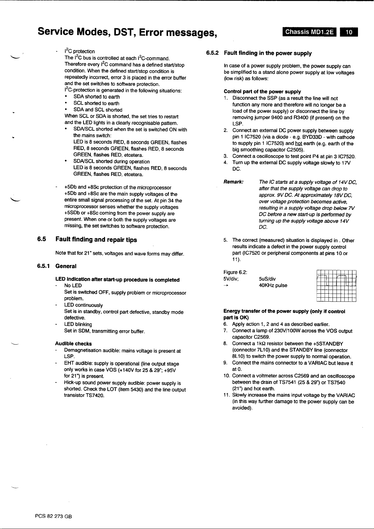
6.5.2
with
ON
seconds
34 the
are
are
Fault Íinding
In
case of a
power
be simpliÍied to a
(low
risk)
Íollows:
as
part
Control
oÍ the
1. Disconnect
function
load
removing
any more and therefore will
oÍ the
jumper
power
in the
problem,
supply
stand alone
power
supply
the
power
(as
SSP
supply) or disconnect
9400 and R3400
LSP.
2.
Connect an external DC
pin
1 1C7520
to supply
big smoothing
3. Connect a oscilloscope
4. Turn
(via
a diode - e.g. BYDSÉID
pin
1 1C7520) and hot
capacitor C2505).
to test
up the
exteÍnal DC supply voltage
DC.
Remark:
The lC
statts at a supply voltage
after that the supply voftage
approx. 9V DC. At approximately
voftage
over
resulting in
DC
turning
a supply voftage
before a new staft-up
up the supply voftage
DC.
supply
power
the
power
supply
a result the line
no longer
(if present)
power
supply
between
(e.9.
earth
point
P4
at
protection
becomes
is
supply
can
at low voltages
will
not
be
the line
a
by
on the
supply
-
with
cathode
earth
oÍ the
g
pin
ICZSZO.
slowly to 17V
14V
of
DC,
can
drop to
18V DC,
adive,
drop
below 7V
performed
above
by
14V
6.5 Fault
Note
that
6.5.1
General
LED
andication
-
No
Set
problem.
-
LED
Set is in
defective.
-
LED
Set in SDM,
Audible
-
Demagnetisation
LSP.
-
EHT
only works
lor 21")
-
Hick-up
shorted.
transistor
finding
Íor
21'
sets, voltages
LED
after
is
switched
continuously
standby,
blinking
transmitting
checks
audible:
in
present.
is
sound
Check
TS7420.
and repair
start-up
OFF,
supply
part
control
error bufÍer.
audible:
supply
case
power
the LOT
mains voltage
is
operational
VOS (+140V
supply
(item
tips
and wave
procedure
problem
forms
or microprocessor
deÍective,
(line
for 25 & 29';
power
audible:
5430)
and the line
is
may differ.
completed
standby mode
present
is
output stage
at
+95V
supply is
output
The
5.
results
part (1C7520
correct
indicate
(measured)
a deÍect in the
peripheral
or
1 1).
Figure
6.2:
SV/div;
+
Energy tÍansÍer
part
is
OK)
6. Apply action 1
7.
Connect a
SuS/div
zlOKHz
pulse
power
oÍ the
2 and 4 as described
,
lamp
of 230V/100W across
capacitor C2569.
8.
Connect a
(connector
8L10) to switch the
Connect the mains connector
9.
at
0.
10.
Connect a voltmeter
between the
(21")
11.
Slowly increase
(in
avoided).
1kQ resistor
7L10)
drain of
and hot earth.
this way
further damage to the
and the STANDBY line
power
mains input
the
situation is
components
power
supply
displayed
supply
pins
at
(only
iÍ
earlier.
the VOS
between the +SSTANDBY
supply to normal
to a VARIAC
across C2569
TS7541
(25
voltage
(connector
and an oscilloscope
& 29)
or
by
power
supply can
in .
Other
control
10
or
control
output
operation.
but leave
TS7540
the
VARIAC
it
be
PCS
82 273
GB
Page 20

----------------
l
Protections,
The wave forms Íor
Mains
lOVAC:
2OV AC:
4OV AC:
65V AC:
>
In case
or the voltage will
1. Figure
2. Figure
3.
4. Figure 6.6:
Fault
6.5.3
When the horizontal
simplified to a stand alone'switched
voltages
1. Disconnect
2.
3. Conneot
4. Replace
5.
voltage
in
65V AC:
of a
6.3:
Mains in 10V
10v/div;
6.4:
Mains in 20V AC
20vldiv;
+ zlokHz
+
Figure
6.5:
Mains in 40V
S0V/div;
+
Mains in
S0V/div; SuS/div
+
+
finding oÍ the horizontal
(low
Discoínect the
current
(between
level
pulse
at the base
PCB).
Connect
FaultÍinding
the Íollowing
20kHz and VOS
40kHz
ztOkHz
zlOkHz
Stable situation,
feedback
exceed 140V
AC
1Ous/div
SuS/div
VOS3OV
AC
SuS/div
ulokHz
VOS8OV
65V AC
40kHz
VOS
circuitry itselÍ
risk)
as Íollows:
the
set
SSP
an eldemal
measurement
the HDRIVE
0 and
a oscilloscope
output transisto r 7
Possibilities:
1. Figure
6.7:
point
L3; test
transistor
S0V/div;
at collector
(7420)
lOps/div
Currertt Írom external
approx. 100m4
Obseruation: normal
and VOS
and
VOS
and VOS
problem,
pulse
pulse
pulse
14OV
Írom
mains.
removing
by
50V DC
possibility
by an
5V); duty cycle
oÍ TS7410
to test
42Q\.
line
DC
supply
pulses
l6kHz
mains
voltage
7V5
30V
80V
1,10V
40kHz
so
the
situation
(95V
with
circuitry
is
defective, h
mode
all cables to
(or
40V DC)
across
eliternal LF
(near
LOT
point
L1
output
and 100mA
and
aÍe
given:
Repair
and 140V
will not stabilise
21')
ffiffi
l+-t-t-L.trl-t-1-l-lJ
H*#fll-HrflH
fffiffiHtÏf\ffi
rfiiïftj-tH
n--|-rï-rrn-t
ffiffi
Ht+++-llt+i-t_1
Íïï]ïflï-ïïÏ]
F+#+fl-I-rt-fi
frrï--rm-n
ffiffiF
ffiffiffi
l-t--]----l-ff-1
ffiffi
ffi
n-n*-T-|-Ít
can be
supply"
C2400.
generator
50olo) with a t6
at the side
(collector
low
at
the SSp.
supply with
[fTL
of the
oÍ line
suppty
kHz
current
tips
Correct hóÍizontal
Note
that ihè amplitude
Írequency
2.
Figure
L3; test
transiBtor
S0V/div; lossidiv
Line
Current from e)dernal
appÍoximately
Obseruatlon:
Causes: horizontal
3. Figure
L3;
test
transistor
SoV/diq 1ops/div
Current
approx
Obseruatlon:
Cause: horizontal
When the line
only a number
does not
e)Íernal DC
4.
Figure 6.10:
L3;
test
transietor
1O0V/div;
Current ftom
approximately 150mA
Obseruatlon: flyback
Cause: flybackcapacitor
5. Figure
L3; test
transiÉtor
1OOV/div;
Curretlt from
Obseruatlón:
Cause:
generator.
of the
6.8:
point
at collector line output
(7420)
deflection open'.
small
supply current
linearity
S-conection C2427
6.9:
point
at collector line
(7420)
from
external DG
500m4 !!
fast oscillations
deflection coil shofted)
show the oscillation
supply
point
at collector line outpui
(7420)
1OpS/div
e)dernal DC
between, 150mA
6.11:
point
at clllector line
(7420)
1OrrS/div
external DC supply > 1A
2
from
short-circuit in
(e.9.
circuitry
oÍ the signal strongly
DC supply is
100m4.
pulse
followed
deflection
L5421
coil
supply
and 500mA suppty
deflection
deflection
of windings
is
not completely
are shorted, the wave Íorm
is
approximately
supply
time is shofter,
pulses per
cycle extra and
morethan 1A
picture
EHT
to Aquadag)
depends on the
by wide
coil open
open
open
pulse
and
output
cunent
(e.9.
shorted
and the curront of the
200fnA.
line
shorted but
is
one exta
supply
cunent
pulse
C2425 open
output
suppty current
tube
100mA
in
Page 21

Service
Modes,
DST,
Error
messages,
6.5.4 Fault
the video
When
that there is
ïDA8366,
For
measuring,
the aeriAl input
oscilloscope
triggered
Normal
1 . First
16, | 7,
are
Figure
Red
CRT
1O0V/div
100us/div
The total
16 TDA8366
The TDA8366
TDA8366
<
> 4.5V :
2.
Secónd
measured
Red, line
measured.
-
-
Figure
Red
R43
(upper
SOV/divAC;
100!s/div
finding
"no
controller
there is
no
problem
a
the RGB
connect a video
with a white
field
with VDRIVE+
start up
phase
oÍ start up; 4 white
1 8)
and the main
better visible ff
6.12:
(pin
8 oÍ connector R43
panel)
and
DC:
beam
during
4.5V :
set remains
set continues
phase
and the main
16 is
differences
compensated
when
the
phase
with
6.13:
(lower
line)
on the
CRr
line)
sun
picture,
lC
picture
and
with
ampliÍiers or the
ftequent. A
at
procedure
the
green gun
current is measured and fed
19)
0C71
checks the voltage
these lines
of
start up; each beam is
Green
and
between
diffeÍences
3, otheruise it remains
(pin
8 of connector
panel)
(pin
6)
protection"
no
part
TDA8366-4C)
protection,
no
the BC_INFO caused
pattern
pin
picture
and
picture
generator (e.9.
to the tuner.
picture
stable
4
511.
measuring lines
picture
is muted
tube is
on the
(pin
6)
pin
at
phase
in this
up
start
with
picture
is
still muted.
line 17
is Blue. BC_INFO
the lines
are minimal the
(guns)
sreen
cold);
(problem
it is
most likely
by the
tube.
PM5518)
Trigger
is
obtained
(wave
1
6 of the
phase
separately
are
set continues
phase
in
[HfIFIl
'
f+JJq+t+{4q4
if
(lines
forms
back
to
2
Line 15 is
2
the
pin
is
l-TT-TH-tTf
.FlTTfmmm
H-i-lt_t-t-l
at
15,
in
start up
bright
picture
hangs in
phase
white hórizontal
is darlt
first
picture
6.12.
(1C71
The
1. A
the
(set
Oscilloscope
like figure
TDA8366
OK
There should be 4.5V
Possible
problem:
TD48366, there is
components)
2.
Small
rest
the
(set
hangs in second
In
horizontal rcd,
oÍ the
TDA8366 is OK
Possible
picture
Measure at
problem:
tube are bad
pin
R or G or B liÍle) is/are
ampliÍier(s) or
gun(s)
3. No lines visible
pin
Measure
-
0V:
-
5V:
-
Pulses
16
:
oÍ the set
19),
can be identiÍied:
line
phase
oÍ start up
oÍ the voltage
picture
tube
pin
at
16
iÍ there is
a defect
(in
at the top; the
procedure)
over
and RGB amplifrers
TDA8366.
present
no 4.5V
one
or more
the BC_INFO Íeedback
green
and
pictuÍe
is
phase
one or more
'16
TDA8366
smaller; the
is/are
(pictuÍe
TDA8366;
Check
blue lines at
dark
of start up
of the
which feedback line(s)
corresponding
Íaulty.
dark)
possible
TDA8366
measuremênts:
(sandcastle
supply voltage)
Check RGB
short
now there will
continuously
pin
16
amplifiers
TDA8366
be measuring
phase
5V,
bypassed)
there is a measuring line,
TDA8366
Measure
panel
is
OK
on cathode on the CRT
iÍ the measuring
present:
+
Yes
BC_INFO
no HEATER voltage
or
RGB
ampliÍier
rest
guns
the
at
looks
pin
oÍ the
loop.
the
procedure)
guns
oÍ
the
and the
ground,
to
lines
1
and 2
so the
lines are
circuit is open
problemNo
oÍ
are
16 oÍ
top;
(the
(at
is
3. After
staÍt up
cut-off
points
compensated
proceduÍe
RepaiÍ
Typical
situation:
-
Switch
-
In a 4:3
compressed"
-
In a 16:9
picture
the
of the R, the G and the B
continuously.
picture
no
the
set on.
"pictuÍe
press
set,
mode.
set,
shift down
the
present
is
and no eÍÍoÍ
size' to
switch the
picture
and differences
gun
are
codes
set to
with the
cursor keys.
in
"16:9
Page 22

Protections,
Faultfinding
and
Repair
tips
PCS
82
274 GB
Page 23
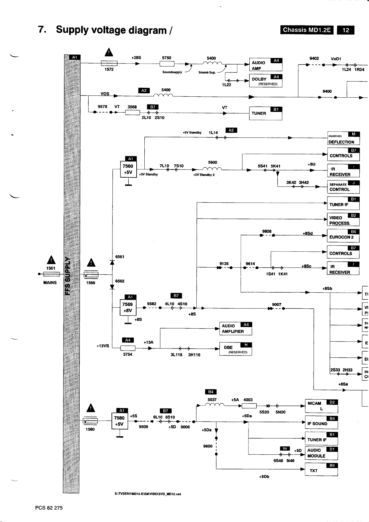
7.
Supply
voltage
diagram
/
trE
Eil
57í)
Sounds0pply
54oo
+svst
S@nd-Sup.
ídby
5400
1L14
trEl
940,2
VoDl
1t24
I
1R24
A
1501
ilÍi'...-j
tt6a
A
A
E
3754
+134
6L10 5510
-.
I
3L116
E
-)-{-=-+--+5D
9q)G
3HÍ16
TI
vl
:
sl
:
E
EI
stl
Cl
PCS
82
275
stïvsER\
ilDí2-É\Sr|\vtStO\SVÍt_ilDl2.v3d
Page 24

Speisespannung
E
5L19
5L19
Schaltplan
3tt61 +13D
/
1L92 íF92
Diagramme
-
VFnmG
de tension
d'alimentation
nil
*13D
Eil
ls54
E
í1m
E
1W54
Page 25
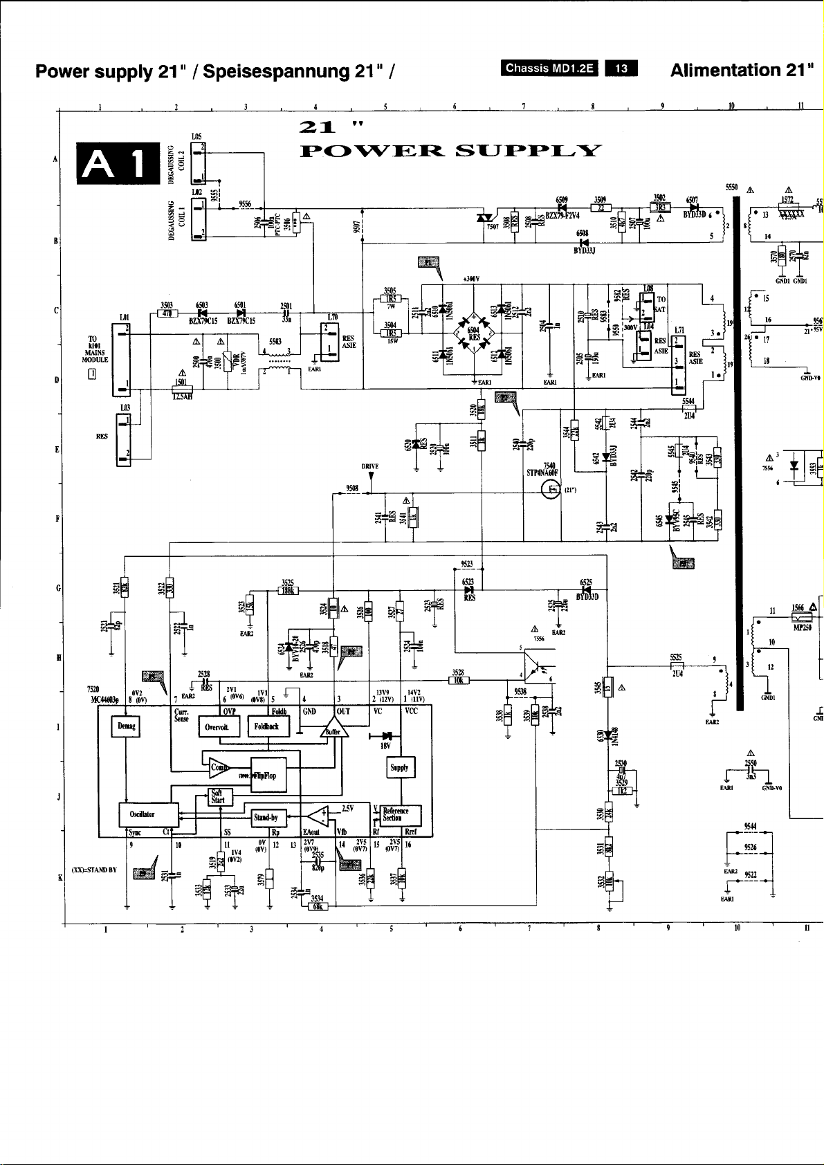
Power
supply
21"
lSpeisespannung
21"
I
@E
Alimentation
21"
EIIË=
2=
m
tt0l
MAINS
MODULE
Til
E
2a-
"
PO\AZF'T<
SIJPPI-Y
^
*
I
r
-J-l-l
ïlsF
i:_l
"rnn
ífv2l
luYJr
Page 26
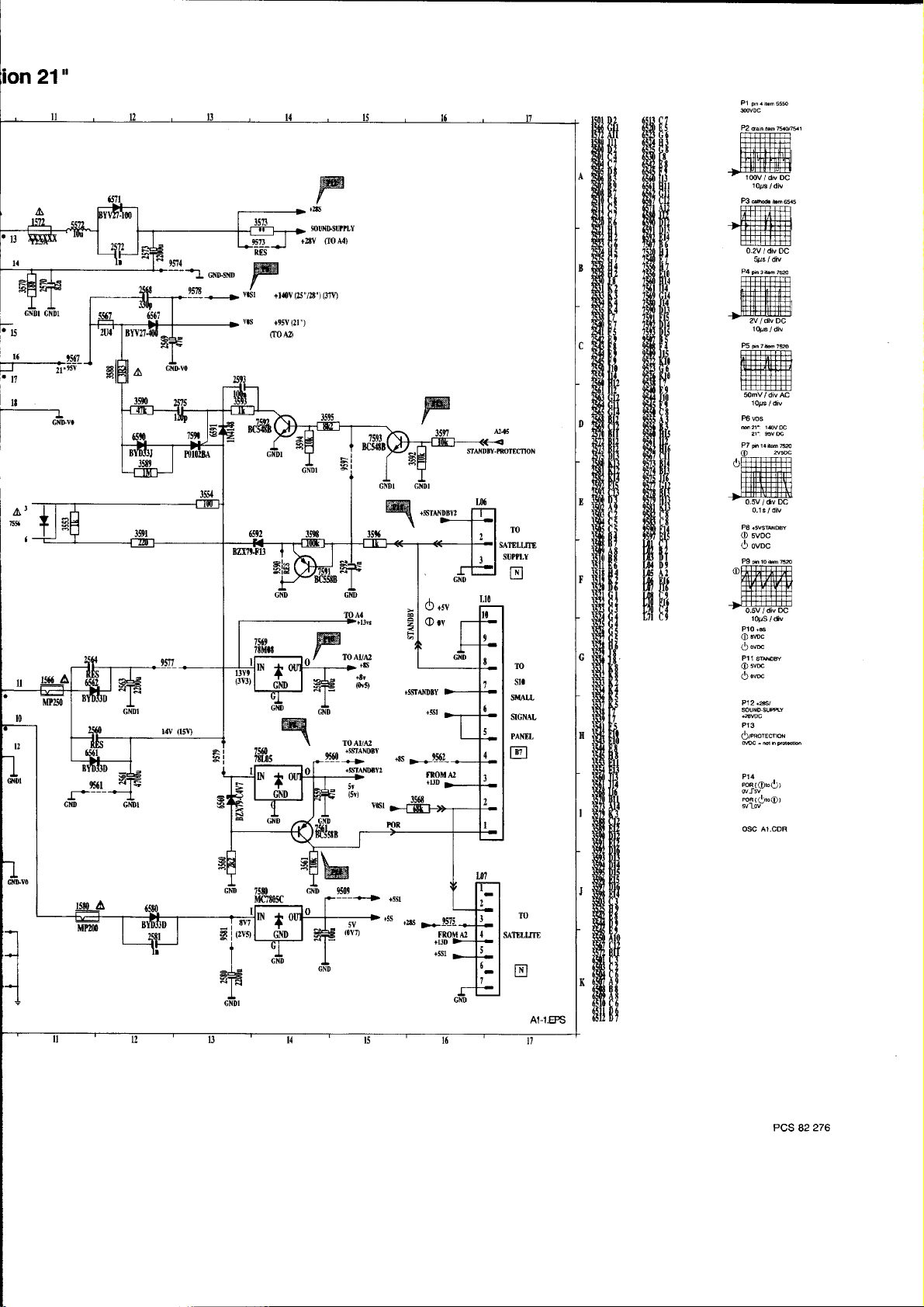
w
r
+2lS
>
SOUIIDSOPLY
>
(I{l
+rSV
P2
Íifi [í
fitrFi
frÍtËtl
A4)
ffifi$
Ëil [l
ddnilêm À@!1
ÊIlIrnT-.I
|*|-l#
F+ffir
,[1:m
-
lmv
/ div DC
P3cdÉihÉs
0.2V / dlv
5!s / div
DC
ljl.
ló
!
.11
ll
t---.:.
I
I
I
fiÍ?
2r'w
Cr{r}vr
!51!---
vór
vs
+r{v
+95v
(r0
(2s"nt,)
(21")
A?)
(37v)
ffi
I To^tl,'
TO AI/42
+ssraNDSY
0{í|
+5STAI{}8Y
*rs
1*9!8-
+55l
ÍloM A2
+BD
L
f#
$NDN.m[moil
m
sIa
SÍIIALL
SIGNAL
PANf,L
E
íffifif
Íffifi#
Í#[t
tifi [.1
ïifi tÈ
*fi Fï
950 D9
fi$ [ï
ffifi frt
i$lËfÍ
ffiffi
hï[ï
I,Í4 D9
IT5 ÀI
w ftt
tr[t
SmV / div AC
loris / div
P6
bs
P7Ér.íomM
(D rsc
,r,[1 lTfrTffll
"l..1..l..l..1..1#
Hrl1ffiÍffi
HTIHIIH
ffi
)ffi
0.1s / dil
O svoc
ovoc
ó
m
hro,h6a
offi
ïYfËlt/-H
FEFT]+TFTE
+bH*iJié'
l0/S/dv
P10.6
OMc
OVE
O
Pl1tuw
OwÉ
óow
P12 +61
P13
oFrcrECnd
Pl4
coqrOrór
@!(t bO)
M
9509
-+ss
í0Y7)
ras
16!5?l
Flot
TO
SATDLIXTE
E
A1-1.EPS
osc A1.oDR
PCS
82
276
Page 27

Large signal
panel
/ GroB-Signal
Platine / Platine
Íorts
signaux
L01 J10 2545H6 SmKg 375649
fto
L02
L03 J10 2s54 E9 3s05 K7 375a B9
L04 K6 2555 Ero 3506 H9 3759
L05 H10 2557 E10 3507
L06 810
L07
C10
L(E K7
D10 2S3
L10
Lrl As 2564D8
A3 2$5810
L13
L14 As 25€aE6
Lls A3 2569 F6 3s20 t8 540 C3 7ffiC2 ms 83
t4 257087
t17
J4 2572D8
L19
122 C7 2573D7 3523 F9 911 K5 7m3 84 SO8 A5
v4 J1 2575 D6
gf
L25
410 2581 D8
L28
L38 A8 2582D9 3527F9 v60G2
L39 tr
L70 K7 2593D7
J8 260082
L71
L91 F4 50283
L92 F2 260342
1116C9 2604A2 3533G10 s525F8 9004K5 9751 A7
t2ÍJoC7
1463 E2 2606 83
1566 E8 2607 84 3536 F10 5545 G6 9007 K4 9754 À8
'1572
E8 2608
1580 E8 2609 85
2400 D3
2401 D3 275r A9
2409 K3
2t10K2
2411 J3 2756 A6 354s G6 il21 Gs 9405 C2
2112R3 2760 A9 3s4 G7 U22Fs 9406 C4
2419 E5 2763A7
zpots 2764CA
212383 2765 A7
2424G3 2766 A8
2425 H5 2776 A6 3556
2126F5 277AA7
2427 F3 2787 A7
2429c)3 2788A6
243283 2789
24:|3Js
2434F4 3401 D2 358C10 U6282 S23 F5
242J2
2450J2 3410K5 3573C6 64A0E4 9425F4
2451 D2
2460 61 3112 J3 358A E6 6€2 D4 9427
2461G2
2462 E2 341 5 K2 3590 D6 6503 K8 9436 G2
2463 E2 3417 J5
24UC2 3418 84
248582 3420 G5 3593 D6 6508 t8 9442 H5
2ffi A
247085
2471 85
2472D2 34e.H4
2479D4
2ffi Es ss G3 3601
2441 D5 343s
2447 C6 3436 D4
2500 J9 3443 | 1
2fi1 K7
2WF7
2n5n 951
fro
2506
297 G8 3453
19
2508
2510 J6 il55 D2
2511 J7 3456 D3 s6r2
2512
J8 34s7 J2
252019
2s21 G9
2522G9 3463F2
2523G9 U64D2
2524F9
2525G8 346685
F9
2526
2528 G9 3470 85
2s30G9 3472F2
2531 G10 3478D5
2533 G10 3479 D5
F10
2534
2s35 F10 3481 D5
2s38F10 3482C5
2540 H7 3483 E5
2s/1
HA
2542H7 3487 D4
2543
G7 3500 Klo 3754
2544G7
F6
2550
2s59
2560 D8
2561C7
2580Ê9 3525G9 U24ES 760582 961r
2592 D9 3528 G9 5/,61 F2 nÊ| 86 9621 81
266C2 3534 F10 5542G7 9005
2750 Bg 3539 F10 5572 D8
2752
275587
3400E3 3561 D10 6460Gi
340282 s570 E7 6463 E2 9424 E4
341 1 J3 3579 G10 6481 D4 9426
y14^4
3421 C5 3594 D6 6509
3430H4 3s9sD6 6510J7
343'1 H4 3596 D10 651 1 J6 9451 G2
gS
3M
3450 J1 3606 83 6542G7
up J2 36m 83 6S0 C9 94m D5
3454 03
961 H1
3462F2 36ís A2 6590 D6
ffis 85
s67
3480 D5
v84
3502 G8 3755A9 7520F9 957s C7
3504 J7 3757 89
19
D9 3sm t9 3781 86 7561 D10 9583 t6
3509 H9 3762
3510G8 376386
08 3511 H8 3764
3512H9 376588
3518F9 376688
3519G10 376798
3521 G9 5401
3522H8 5410J4
3524
3526
3529G9 U62F2
3530G10 5463J1 9001
3531 G10
3532G10 5503J8
3535 G10 5544
82 3537 F10 5550
3$a
3t40 H7 5750
A9 3541 H7 5751 86 9{3 Et 9786 A10
392H6 911 K5 9404C1
3í5 G8 6423G5
3s53 E9 U24F5 9408 D2
3554 E9 6425
3555
3557Ê10 U2aO2 9418C5
3558 E10 6441 J2
3559D10
A8 3560 D10 6457 J2 9421
358906
3591
3592 D6
3597C6
G3
3598 D9
G3 36m 81 6523
36m A1
3604 C3 6s25 G8
D2
3605 83 6530 G9 9465 03
J2 3607 83
J3 3609 93 6561
3610 A2
3611 A3 6S7
361 3 83 6572
3614 84
3616 A2 6591 C7 9526
361782 6s92E9 9s38E10
Sra C1 6m
3619C2 6601
85 3620 A4 66t0 C4 9544 F9
3U1 C3
3623A1 6751
3624A2 676387 9555110
3625 82 6764
3626 C1
3627 81 74'11 02 9561 C8
375086 7420t5 9562C10
3751 86
E5 3752 A6 7450 D3 568
3753 A8 74{n D5 9573 C6
3760
H8
5/'21
F9
5430 H3 7606 84 9615 A3
ímD4 S02K4
Fro sS7 Ê6 94m Ê3
Dro 6426 F3 910 K4
4427
E10
6450D3 9420F4
6501
E9 6504 J7 W0 H4
6507
6512J7 9453G1
6513 J8 955 G5
B1 6520
6524 H9
6v5 H6 9470G2
6S2 D8
6571 D7
84
6S0 D8 992Ha
6750 86
7410K3
7421 H5 ffi7 E7
7507 t9 9574 C6
89
7540H8
7541 H7
7555
B9 7556
A9 7s60
A8 7569 89
7580D9
A7 7590
7591
7592D6
7593C6 960483
D2 7601
76n2B2
G4 7ru 83
26049
n63gï
9003K,t S750A7
G6 9006 K4
F7 9m K5 9755 Ar0
g,ml
86 W2E1
SO7
F3 sog G2
C2
9419 Ê5
942284
K8 94í)0J4
9441 14
G8
H9
9443
S50J3
H8
9460 G2
H8 9461 F2
9462F2
94U D2
9466 C4
D8 9€ Cs
9507
E6 9508 Ha
9509 C9
D7 951 1 Ha
9523
84 9y0 G6
A2
9541
9il5
86
955016
88 9556 r10
9560
95nCA
9578 C6
E10 9s79 D8
E10 9581 D8
C9 9582 16
9590 09
9s97D9
D7 9601
D9 9602A5
9603A4
S606 84
C4
9607&
9609 84
$2041
9625A2
K3
962682
965085
K3
9752 A8
9753 A8
9758 88
D2
9759 97
978r A6
E1
12C2
H4
F4
l5
E1
19
H9
F9
H8
H6
C8
E7
.'z
8968.r,5,18,
,t;
82
t
gr
I
Í=-'
i'ti
84
ËHË1.Àl
r-
E!7F
n|-_l..+r:.i.,-
"l
€;'"q
-ÈR
'ïnd
'
ars6
r-Cl-
Z LE6O
!r
I
[-.-:-]::l
-
;.
PCS
82277
Page 28

liJ
-lrvNers
isdv
r_
_i
ï'ls
t.,i
JCFE*?CL
tl
l,l
lc__;o'.
.
." -
sali.
-l^t_
|
:l | -Tnr--r
'ï
--]_r-
'
.
|
r.r---1.-r.
Ë
Ë..
:ll
à
-t I
àr r'
Itr
e!:le
ït"
ïiffi-,"*Eï
ï;
6ïiË-il El i'
ï;a-++*
L-,--,,
|
-tE
sN
nËl-rr
m
-Ë-
\ht
z
Ë
'l*iil'mi*f,#*
l*HYï
I
I
r[+l
r
r'..
-
#+h
slTTln'E
'
fË;;-E S-
ta=l:
I ;.*
ffit :H$l*ïP
ÈilËEFH4+?+-r
ám
i 9NINdVll ldvd
,,'n@.[r
:
fAT-l
Page 29

Power
supply >
E[Ë=
21"
Speisung
/
>
24,,
PO\AZE-I=
>
21"
w
I
SI.JPP.-[
\ +:rv
@@ftr
Y
Atinr
Page 30

Alimentation
>
21"
2t"ws
U'B
CRTI)
crT0l
350? It It
25'SF
ts/2''BM
ctr02
CRTO4
gE
stAl{DBY-tt{nf,cnol
l$l
350t)
3512
l56t
75&)
216Í
llfiLs
sunl
RXS
lr5
1|rt
MCïe5C
32'WS
CRTfi
It
2.12r ll0{teg
-
25'TES[,{
C(Itr'
SUP||6
Tl.l5A
IMA/]87V
lt5
l00k
MCtt{tsc
20"ws
CRT!8
2.tr
sl
SUPIN
TI5AH
IMA3ETV
2v2
t2l
L7805AC.V
29'SF
CTTI9
138í
ilfii
fi[f
60 ll3
ft 8tl
61 Cl2
fi$fi
ilffi
56 EIO
il Ët:
ilfil
ffiffi
fiftit
t{bl
$Èï
W-
t4v
0sl,)
7560
7fi.S
ffi
I TOAltA2
9560
+s
->
+tv
(ovt
TO AUA2
+5SIAIDlY
-.-}
M
9509
ËlS;ï .F
+sSIANDBY
{5Sl
+tS
{5Sl
+5s
+2ts
>.-!15-
fROM
+l3D
+ssl
Ul6
TO
SATELLIIE
SUP?LY
tNl
E
ilnfi
ítfifi
Hffi
212
tBl
iffi
TO
sl0
SMALL
SIGNAL
PANEL
@
m
I
I
SATETTITE
E
PCS
82 278
Page 31

Horizontal
output
Horizontalausgang
/
H(OFR.I-OhTTA.I-
/
rE
VDUV8T|VD
À1.21
19-
-voor
.
íT
4'
(9
{r)
Ë
r
Í
I
I
L
l*s
t{00
fffil
"**
t--'
1l
i!-
-l
tot
r
ït,
E
f,,,
0r
t{6
[.,
;l
I
I
I
I
^
5{I
l:
'1
al
:
ódl
í&
=i
L
L1 rcs
mn21'1{WC
w
e6fi
ww
m69$9tx9{,1,eu
---t
È---f---t -------
gddcNDvtd
L2catsimzaro
tm-m ffi ffi #
ffi
Hll+ï]ïi,H
q#ï-lÈffi
ffiffil+i1_+++]+ |..]...]...]...]...].'']...l+L..]Jru
-}ffiffi+ilffi
lqgs
/
L3&r6orrêh7t2o
'# +il
l+r-+-+r-r.{r-+-!-r r,Á.r!++r-fÁ] H-+rtlil
L4
ffiTfrffiH ffi
div
10!s
/
Oiv
sms / div
L5+j3D
14wDc
L6m,ue.
L7lL8vFilME.+iffip
sn
|
Lgilo LlOM_coMp
EEtEtr rr
ffi+HW
5ms
div
/
ffiffi
ffi
5ms / div
0V2
2qJs
div DC
i
/
div
Lí
3 rc-PRo
0v2rc
=ov-l
f+
osc A2.CDR
PCS
82
279
Page 32

Sortie
horizontale
(ro{dt
$uNlt{tíÁ|l8
À+t5
uu
m
gl
MODIJU
E
ot
Mtu
ccr
INL
E
ïo
ES
M[
gGMI
tffi
E
tÍl'
ltu
taD
lff
lb
lh
Ih
lh
lfr
lh
t.
t.
tb
trÉ
l^
lo.
l.
t:
lg
11t
|
lu
I
t-
l3s
l$1
lhl
íilt
l{&
|
t:
I
I
I
IE
lrE
I a
lm
lo
li
lEs
lrc
t5b
Itr
lÍr
IC
lfr
lft
lK
IT
t-
lln
l&
tan
ln
lfi
lfi
lE
tm
lr&
lrs
t-
IM
IK
tu
Irru
m
til
l*
:ir
3l
l:
AIW
uco[
cilLla?
MN
t\utÁ
r*I"t
Id'Bí
rmiu
m
rÉn
IRI{
IUT
m
Jft
tt
0
0
fl
tr;$
H
a
lt
IG
fl7
&
Its
m[m
hc
Vertical
ffiE\ ffiFi
output / Vertikalausgang
ffi[ï #ir[í $flfiï ffi[r
\ZEKTICÁ.I-
EEI
Sortie
/
frfif;{
ffi[ï
3601
ffiz
3d)3
3ó09
x25
x26
36n
7ffi
xzt
9ó25
frHB1'
3R3
3R3
3R9
?}riz
lm
10
l0
RES
+
verticale
fi:í8[t
Mnb\
tJ29 D3
MI B3
#$J
4R?
4R7
4t?
2M2
tm
RES
ry
+
RES
6R8
6R8
6RE
Itz
lm
4R7
1m
8C5578
+
RES
Aut
A2.u
E lrru?
vDffv' -t\
VFMMET
,.Jry}
Ao?4
vFxÀM8.
1N4148
Al^r
N1?
ffi
5V
/
sms
F4wmril
F2w.
DErufrlON
ffiffi
div DC
div
/
trV+)
10ms / div
F6m:+
lavm
l-5=ovl
osc A3.CDR
Al ruDlo-L-3KHz
(wumehded)
Al0eq.d
l$zdgH{ins.dft)
ffiffi
ffi Hf,+f,ffi
H+++fF]#
50mV / div
0.5ms / div
A2&oro-R-ÍGz A11m4or
(d0mkdinred)
0.5ms / div
++H#++fl
AC 0V2 / div
0.1ms / div
3xHzld(iE Wmd
AC
Page 34

I
audio
amplifier
/
Ton verstàrker
lAmpliÍication
138 Flo
l39 n0
audio
ffiw ffiffi
ffiiÊi ii#Hi
EE
w
TO
AUDIO
TÁNEL
E
ffiffi ffiffi
ffiïffi
AIJDIO
.u*
{FRoM
--f4lp-
Al)
eJ.
-l
-u^
SND.SUProY
(FR6MAr)
ffitr
\\,4PI-IFTFR.
- ï -r'hil*
I S?5n ISOUrc-SUr
'-1ír*
CND.SOUND.SU?NY
Ar@
ffi
I
CND,AUDIO
DBÊ.R
9?55
! P.GNDI
P.CND
*,
nu,
POm
Ào,l?
TO
DBE
PANEL
tr
(RESERVED)
ï0
DBE PANEL
tr
(RESERVED)
n50
n5r
2752
nil
n6s
TN
nn
nE9
3154
3156
3157
3?58
3759
3760
316r
3762
316/
n@
sNml
2m!
1{mr
1m
BC!t8B
l0l
l&
8t2
2y2
3K3
4t(3
nx
56K
lm
812
ffi
^T'ls758
^?'
9?51
nó0
2V9
s0ND-ru88
(eti
plop)
SNDO2
SNDO3
br
W!
lu
lu
4u?
4t1
l!
2k
lu
ER2
2Y2
3(3
4Kl
22K
56K
tK5
1K7
10R
5K6
l!
1000u
lm0!
470t
Ut
h
8R2
2Y2
3K3
{Kl
22K
56K
1t8
2Í2
1Ll
8t2
BC54EB
Iomu
lmr
I15
170p
{rt7
It
8C5488
silch-o!
t€m
Als
(di
silchofi plop)
-+E
P.GND
ÁOu
SNDL+SPFAIGS
m,la
sNo*suew
SND,-SUBW
A4.CDR
PCS
82
280
Page 35

Small
s11
s15
s20
s33
s40 F7
s41
s42 D5
s43
s46 F4 2168
s47 D4
s54
s57 86
s60 85
s75
s80 c7 2175
s81
s100 J5 21T7
130
131
132
1000
1031 H3 2182
1032 13
'1100
1116 t5
1117
1'118 t7
1119 t7
'1122
1123
1650 D7
1651 D7
1700
1800 F1'
't801
'1802
1803 F1'
1804 C1.
180s
1806
'1807
2004
2006
2007
2008
2009
2032 t2
2033
2034 t4'
2036
2037
2100 Hs'
2101 H5-
2102
2103
2104 H4'
2105 H4'
2106
2108
2109 15
2111
2112 t5'
21f3 15'
2115 H6'
21.16 F6'
2'117 F52119 F6-
2122 H6'
2123 H5'
2124 H6
2125 H72126
2127 F8
2128
2129 H6-
2132 H7'
2133 H6'
2135 F6r
2136
2137 H5'
213€ H7'
2139 H7'
2140 t6'
2141 t7'
2142 H7'
2143 H7'
2144 t9
2145 t7'
2146
2154 H8
2156 J7'
2157
2158 J8
signal
J6
2't60 t7'
C6 2161
t2 2162
A3 2163
2164 t7'
C8 2't65 t7'
2166 t7'
D5 2167
2169 H6.
G7 2170
2't71 H6.
2172
J4 2't73
G3 2176 t6'
F1 2178
C1 2't79
A1 2t80
J3 2181
2184 la'
F4
2196
2600
t7
260t E8'
2606
2607 D6.
G3
261 t D6.
G3
2650
2651 D7'
2652
88 2653
2655
F1.
2657 E7*
F1'
26s8
2659
2661
c1'
2662 D6'
C1' 2663
c1' 2665
J3' 2685
t3'
2700 85.
13-
2702 A8'
t3
2703 A8.
14
2704 87.
2705
H2' 2707
2708 A7'
H2-
2709 87'
H3
2710 A6.
2711 A5.
2712 BA.
G5-
27'ts A5
H5'
2716 85
2717 A4.
2720 B,8.
Gs
2800
15-
2801 G2
2805 c2
t5'
2806 G22812 F2
2813 F2
2817 E2
2830
2835
2836
2a37 M'
28r';O
2841 Q2
2842 C2.
F8
2A47 D2
2A52 D2'
J7-
2855 82
2856
2A57
2858 92
2a60 C2'
G5'
2875
2A78 B'4*
2879
2880 A3
3003
3007 J3'
3011 J3"
3012
3014 J2'
3030
H7-
3031
3032
3033
J8r
3034
303s
panel
t6'
t6'
t7'
J6
J7-
H6'
J5'
t6
t6'
t4
H5.
F6
G8.
G8.
H7.
c8r
D8
07'
D7"
E7E7'
E7r
E7'
B7
D6'
D6.
C5.
D8-
8787'
F2
D5
82
A2
C2
82
82
A4
83.
J3-
t3-
H3.
H3'
H3'
H4'
H3.
t4.
/
3036 H3'
3037 H33038 H3.
3039 H3'
3040 H2
3100
3101 H5'
3103
3104 H4'
3to5 H4
3106
3107
3109
31t0 H5'
3111
31í2 H5.
3113
3117 t4'
3119
3121
3122 J6'
3124
3125 J6'
3126 J6'
3127 H5-
3128
3130 F8'
3131
3133
3134 H6.
3135
3136 H6'
3137
3138
3139
3140 H6'
3141
3142 84
3143
3144 85'
3145
3146 84'
3149 H8
3150
3152
3155
3156 H83162
3164 t6.
3165
3166
3167
3168
3169
3170
317'l
3172 16'
3173
3174
3175 J6
3176
3177
3178
3179 H4'
3180 143181
3182
3184
3185 H73186
3187
3188
3189
3190
3191 G7
3192
3193
3194
3195
3196
3197
3600
3601
3602
3603
3604
3605
3606
3607
3608
36'10
361 1
3612
Klein
3613 E73614 E7'
3616 E83617 E63620 E7"
H5'
3621 E3
3623 D7'
G4 3624 e7.
3625 E7-
3627
G4' 3660
G5 3661 D7'
H5'
G4 3664 C5
J5 3669
G3 3680 D8J7. 3681
J6
H6-
F8'
F8'
F7'
H6'
H6' 3701 86'
H6' 3702 86
84 3704
85'
84' 3708 As'
G8 3711 A4
H8' 3712 A4
18
J8 3715 86
J7
J7
t7
J7J7
Js
J4'
Js' 3807
J5-
J6
l5'
t5-
G4 38'17 82.
G4 3818
H8-
G5
F5'
F6'
F5F5'
G7.
t8.
J8G7 3831 D5G8'
G7'
c4
D7.
C7 3836 A2
E6'
C7
C7 3A4't
C7 3A42
C6
D6 38/.7
D6
C6
D6'
D3
C5
3662 C5
3663 D6'
3666 D6-
D6'
3670
D7'
D83682 D7'
3683 C7'
3684 D7'
3685 E6
3686 E7'
3687 E7'
3688 C7
3689 E7
3691 E7.
3692 E83693 Es
3694 C5
3700 A7'
3703 85'
88'
3705 87*
3706 86
3707 86
3709 85.
3710 A7
3713 A4
37'14 B5
3716 863720 A8r
3721 A83800 F2
3801 F2
3802 F2'
3803 F23805 F3
3806
G2
G33808 G2.
3810 G2
F2
3812
F2
38'13
38í4 G2
38t5 E4
E2
3816
G2
3819 E4
3820 E4
3821 C3
3A22 F3
3A23 H2
3A24 e2
3825 c2
3826
C5.
3827 C5
3828 C4
3830 D5-
3832 Bs'
84.
3833
3834 84.
3835 82
3837 M
3840
C2
C2
C2'
3A43 C2-
E2
3848 C3
3850 E2'
3851 D2'
Signal
3852 D2'
3853 D2
3855 C2
3856 C2'
3857 82
3858
3859
3860 C2' 7031
3863 D2
3865 D2
3866 D2 7100
3867 D2
3869 E1
3875
3479
3880
3881 A3 7108
3882 833883 83' 7110
3888 82- 71t3
3889 A2'
4002 t4'
4003
4004
4025
4026 854030
403/. H2' 7601
4100
4101
4102 G7' 7608
4103
4104
4106
4107
4109 F6'
4113
4114
4115
4116
4í17
41 18
4119
4160 F7r 7850
4'197
4601 D8.
4602
4603
4604.
4605 E7'
4693 G34700 48'
4701
4702 A8'
4703 48.
4810
4875
4876
4877 B'3'
5001
5030 H1
5031 H3
5037
5'100 G3 9102
5105 J4
5106
5114 H4
51í7 15
5600 E5 9109
5601 E8
5614 F5
5652
5702
5703 85
5704 A4
5720
6003
6030
6031 H3
6032
6105 E6
6106 E6 9123
6107
6108 F/
6109
6111 H8
6660
6661
6700 86
6800 F2
6801 F2 9132
6830 0s
6835
Platine
82- 7010
D2 7030
84 7'lO5 F5'
E2 7106 F7'
A3' 7107
H2' 7119
H2. 7120
A4' 7140
H3' 7600
G3' 7604
H5' 7605
F6' 7610
F4' 7660
F5' 7685
H7' 7693
H8' 7701
J6- 7702
J6' 7703 A5G3' 7720
G3. 7805
t5' 7826
F8- 7830
G7' 7a51 D2'
D8- 7875
E8'
E7'
88' 9006
84'
83'
83'
F3 9013
H3 9100
G6 9.t05
D7 9112
C4 9.t13 E8
88 9116
J3 9117 H4
H3 9118
t4 9121
É6
F7
D5 9128 t6
C7 9129
82
6836 A2
6840 C2
6841 C2
6850 Ê2
7009
J2'
J2'
H3'
t37032 H3'
7033 H2
Hs'
7102 H5.
7104 F5
JA'
84.
7109 85.
84.
t8
71't5 J77't16 17.
H6
J7'
H8
7150
c7-
E7
D5.
C7.
C7-
D6.
D6-
C5.
D8
D5.
7700
85-
A7
86
BA'
G2
C5'
D5.
02.
7867
o2.
83
9001 F3
9002 F3
9003 t4
9004
c2
9005 F3
F4
9007
c4
9008
H2
9009 F3
9010 J4
901 1 t3
9012 t1
H2
9015
t4
9016
t3
H5
H8
9103 t8
H5
9107
c6
9108 H4
t7
9t10 F4
9111
c8
G8
9114
c7
9115 H7
G3
G7
9120 t5
H8
9122 E5
G6
9124 F6
9125 F7
9126
G6
9127 H5
J4
9130 t4
9í3r H5
G6
9í33 F5
9134 F8
/
9135 G4
9136 F4
VIJÓ EC
9139 E5
9140 E5
9141 E5
t4
9142
F8
9143
9145 t4
t6
9146
9l6t G6
9600 E5
9601 E7
9602 E5
9604 E6
D8
9606
9607
C4
E7
9608
9609 C8
9610 C8
961'1 D6
9612 D6
D6
9613
9614 88
9615 C8
9616 C6
9700 A4
9703 87
9704 87
9705 86
9707
87
9708
A6
9709 A6
87
9710
9720 A8
F3
9801
9802 D3
9804 C3
9805 E1
9806 83
9807 83
9808 C3
9810 A2
9811 A3
9813 D3
9814 D3
9815 D3
9816 C4
9817 D4
9818 D4
9819 F5
9820 D4
9868 C3
'=
SMD
component
I
I
_o
ËrË
:r9r
"_'l
:"
ۃ
EU!
fl€
r[rt*
3rss
--E-
---gtll/-
?""iii.'r-'-
rpr
ecre[\'''
"P",rU.
.rrs
E,^En[
I
!=@"
{l
ol
$r
'l
--l
ol
I
ël
W
tËl
E-r
--3Es
N/-\-
E(!/l
ï-
9ta3
,
slr s
-l=l-
-c'c
------
-l Feossr
.l-
|
-l' I -
l,f
lr I
I
r9
l'
I.--t'*
-
JaÍ1
r^1 ,'u l -
-E-
t'8
\-
_
=
.]1L
Ëo'1.
"i;]f4'Ë-
SU'
\?
'7
ïEt
lnr
ts
q
.: ir
Í-1
|
L-
tË
r,.l.i
;
ïr
I
:
i
r
PCS
82 281
Page 36

r
Platine
Tlols
petits
signaux
Page 37

Tuner
+
lF/Tuner
+ZF
/Syntoniseur
+ Fl
@E
1g9q s1 ?q06
El 2i01
iiii irl i88í F i ii83
là6i E't
1t83
Ë,í iiSi
Àe
F',
B I 3il1 3;
TUMR
TUNOO
1000
w9r6s
300?
10K
2106 B9 2113 r9
3l8i $ll 3ï3i Ëli
3ót3 $'i
(BIMOS-IC)
+ IF
TUNO3
TUNOI
u9445
uv9lós
l0K
22K
3007
E5 3101
i8i]
F 3 ii8r i.g
Sti6 Li
c]l 3110 t13
Bii
liii
il8Í $,1 lli; Bii
+5Da
Y
{100 Di6
4101
c10
4118 C
5100 Er4
5105 D 7
I
5106 C14
B12
5114
511i D 9
E
6003
7009 F
6
4
4
7010 F {
7100 Dl3
7102
B 9
7ll9
Dl0
9010
u 3
7
*-rï1
9012
9016
9100
9lt6
9117
1)
ecrutooly
I
I
I
t:
cNoo
I
rr3
9127 B9
B5
9130 Di
c13
9lt2 r 6
D15 9145 B
E 2 9146 E10
8
L=0
U2 = 2t8
N62
*,i'
.
3
s1-01 F 7
82-19 D17
84-36 D
B{-39 B
85-19
+8Sb
Dli
9
t2=2\2
l;7Y6
B?-52
G
Bi-54
7
7
G
87-82 B
88-19 Dl
B8-20
El
I
I
9t27_ _
I
I
ffi
lrH
.@W
ffi++I++F
50mV/divAC
sqps/div
B00l 8002
tt
--T-
GNDT
Vl1
reeND
nll'1tr'''l
2qls/div
cvas
'
LFFF+FFF+
-
0V5/drvDC
ml2
\t
.tr--r-;;.-l
golo
:I-
ïEs
*r'o
-T-
-I-
9ll7 9145
- -
lj
GND5 CNDB GNDBI CNDT
|--+=ovl
OSC_B1.CDR
^ï,
-l-
{ sJ3
I
+1
I
Bcl.t-tonlv
,
Acc
9L4a
^i
I
S?5
\
'<\à
I lsArÊum I lsEPcrRLMArNs
tttl
r--/ ï'/
Slm
GNDBI
\
81-01
I
GNDBI
I<'
GNDBI :l
t-
GNDBl)
Page 38

s100 a
R4
s75
5
5114
fil
Lry
nlo2
4
3V9
|
Inr
-44
7n9
TDA836ó
/
5v8
l.z I
o-*,
?100
BC848B
A3l9
ONDE
B
DESCRIPIlON
rIEÀABLOCK
il16
lt22
m08
2108
31ll
3119
4118
5105
9116
BC DK
STEREO
sYsol
0FwK3953
TPS5,5MHZ
l00u
tn
100
lu
BC
NICAM
LI
SYSO4
0FwK3953
TPS5,5MHZ
2Ns
4\1
rm
lm
0u68
I NICAM
sYs06
oFwK3953
TPS
6MHZ
l00u
rso
+
tnz
+
BG
STA.IIC
SYSOS
0FwG3962
TTS5JMHZ
l00r
rso
lm
+
l!2
B1.oDR
Mp ul
t
Page 39

Video
processing
Video Verarbeitung
/
Traitement video
/
VIDEO
m0 NT m0
D
nd
,l$
ls
tg
{to
a[,
a\n
IO
,tal
9tB
PROCESSTNG
lÍ
(BTMOS-IC)
nd mt
zn
a
:
ll
;
^
3lL
d;Tn-a-dr
SF
I
I'l
1';W
9lI 9Bt
I-a-1 r-r-!---I
GM dA OM M dN
9l|9
tB
I-r-L
M dD'
910
l-r-1
6NM dU
VaàF
idhf,ets@
ffiffiw,m
ffi
)"*rrt*+€ffi+qffi
tus/dlv &s/div
v4bc
bd67Ío€k)
H+{++{++S H:{++g++S
v&B
tumrrs@k v5..3e(r
ffi
2&s/di
62s/dv
ffi
u]+*ll
|m]m-]mm|'1--]-]..m
'Yi"ïf
V6GGRwr
Frr
rc t-rrlTtrTrn E[EI]]4
fiffi>ffi>ffi'ffi
Hm|-rrn
()|l,/li|@llffi
1tos/dr
waF.YM vD
@1616r.0
ffi ffi ffi
OPlotu& w2 d'vrc N2,dturc
lqrs/div rop/div 1oF/dtu
rrltmn.q
(sYrtr
VTcYour
t:]:]::]::;:@]
Hll,L,,",
r:ryr ril+l* H+ffi+fi
'ffiffi>W.ffitFËffio*."".
;ffi
;i1.";.,,.
{ffiry
ËodíbË iM-6
2os/dv
w6.@T vryol,
2&s/div
rïfffffffi
-.fï;id
&s/div tu/di
v&nvrou'
Hf#*ËhE
iidffi
rt=o
Page 40

@E
SECAMPROCISSING
ctvnsroc*on
fl
5B
0r
I
lwí
ntg
twí
I
t
WID
ta wí
9W
ówí
VIDEOCONTROL
DD
I
*l
=r
-Ep
F
"'ffi
I
cnrnoour"r
@l
,6
8Cl
5Ca
a(I
2C{
1Ca
lci
t+4:l
09_82.CtR
Page 41

Synchronisation
Synchronisierung
/
Synchronisation
liflËÍ
ltn\l
liitït
ïiiïffi
li{'Ei lllífii
iifi
ËÍ iiff Fi
(
1í?0 F
li8ó Et
iilí
Be
ïll3fit
9t20
G2
3
9128
G2
82-50 D
6
p.r
Ri-l?
BiiÍhï
83-80 B
1
4
83-80 F 6
s1l
ci
/
@r
lF
sr
ffií[r
83-80
B}50
83-32
t
t
PHASE-C0MP
A308
cffio
SAND
A3!
2!2
3ln
ffi
3!!
SYNCHRONTSAïON
$6
ciór'j7
CNDB2
AJ4t
71194D
3124
4367
(BrMOS-rC)
HDNVE
A1t5
I-j-a-
l0
stl
TO
111
Fl,uprr.fp,,
ïffifi] fr.ft-fffi.1 ffiffiffi
itfij_ft-ifi irt-t-Fri-t-#t
F3,"P?'Y';
,,,
Bryo,
, ,., ,
FF'1'ÉFfl,fFï+B|++l+Ji-1
-ffi-ffi,ffiffiffi
sms
/div
sns
div
/
sms / div
Ll9:,*fgïï
5ms
div
/
Ll1sD
n+rl..ffi]r
1016
/div
Ll2 H-DF rvE
rrn-nrfm
ffi
ffi
ffihffi
nnTnETÍTlfl
>FHF**ï*flfl
-
0V2 / div DC
2qÍ/s / div
l>=ovl
OSC-B3.CDR
Bjffi***
HFBL
83-32
Alos
Al3
4
7
-X-
Slt
Sll
-
PANEL
@
ffi
'ffi
Flt+
50mv
srys
/
Page 42

lF sound
iZF
Ton r Fl
son
1$1ïFl
ilil[i
ilfi['
I
i) SYS04 only
2) NOT IN SYSO4 ( BG LI NICAM
3) SYS01 and SYS04
3037 G2
tfl18 F,
3040 G2 5010 86
ffi38; !Bt+fit
40M 87 6030 F2
4030
04
Í8#
flt
IF
SOUND
(BG
U NICAM
(BGLI
ONLY
)
6031 E 2
f8rfr Bi
íflliËí
ginl
3
)
and BGDK)
9m3 Cl
90lt B 2
mllHt
rï{f,F?
B8
81.3ó C
1
Bl-39 F I
B+39 F 1
8439 B I
at10Êl
tsE-uz ts E
88-39 F
7Z
_-A-A
_t_l
-À
1
^l
88-57 D 8
BE-57 B 8
S2O 84
MCAMLMODULE
z
z
+
^l
l!4
R
=
--Y--
/\
-t
DI
=I
Itdl0
_t
XI
Kl
CÍ'dl0
R
z
Y
I
I
_1l
gndl0
B&3e
L'L'
B74l
ml3
T.L
I
codlo
r.a-'3
I
Ay/FM
+I3Db
+5Da
I
I
ëÊí |
-+
^262
I
*
*
1031
,5
I
1t
|
Y
470u
8!d1o
I NICAM
SYS06
0FwK9260
470u
i
+
;
B4.CDR
K,
Jl/Nlt
sYs08
lFwcg2sl
4'tu
41
r
+
-
[m]tl
tl
oolt
.l | .
+
ll
lr__
I
DESCRIMON
lTEI\,I\BLOCK
1031
t032
m37
3040
4$2
4m3
4m4
4030
4034
5m1
5037
9m1
ml1
9015
èJ=
-l
grdlu
*ïio
BG DKSTEREO
2916
sYsol
0F'rvK9260
0FwG9251
4?0u
:
+
+
39u
BG LI NICAM
sYs04
0FwL94Í
0FwG9353
trftffi
'ffi
H+llrffi
50mv / div
íI/s /
Ac
div
t>=ïv-l
osc_B4.cDF
PCS
82
284
Page 43

Euroconnector
1
/ Eurostecker
1
/
Scart 1
@a
SNDR-SCI{UPUT eme
A2f
or-p
.
EUROCONNECTOR
+8Va
.l!g-n1t
oït
I
lihrl 81frP1
lt8l$l El#Fl
llli [Í Et'1191
ttw x!
gl-rvlt
itui tt Ët#hi
tfltr E3 Bt{tÈr
iil; Bt
30i8 ! t
SNDR-SCI-INPIIT
t[Br B I
ti8t Ê,
lttrFr
ll''8 F 3
l8l2 B 5
lSll c 5
t814 D4
lN[ Et
tllÍBÍ
1il0Bí
{t44 Ët
JlU b"4
3824 F4
1825 F4
I[?4 F Í
lrti
Fd
Jgp_
ooï
GNDA
G_sc_rNpLT
B2.zs
1830 G 5
.18-11 G 6
1[1388
àf,#il
ftgÀ Èt
,ilàFe
í848 fit
9005 0 3
8tBlRl
Elt9 il i
3fi0F;
Bl-l9F I
82-04 C i
82.lóF 7
PCS
B5.CDB
82 285
Page 44

Euroconnector
2
l Eurostecker
2 l
scart 2
ifiiH
iffiËï
fifiËi
iiiini
ffiËi iiilffi
ilf,ii
EIt
I E
.I
I
I
I
I ï
i
,
I Y
SEPERÁÏECONTROL
t
R íÈ+--f-ao--------------
Y-/-n_,r,F----_-r_
r
ll r)<ï
,@-:l-,'------------
r
ll )kuu
iiiiËï ffifl
iffi[
EURocoNNECToR
ii#Êi
-->kqsli
íffil[ ËfiiiÊi
q2J1
#frH
2
*su
Ëi#$
sNDR-FRo\r-rNPur
^r;E
r-l''
*"'
SNDL.FRONT.INPI,Í
I
A(11
9ql-
Á4zr
tff
n"*,
C.FMM
YSBS tr?
ovt
rut
I
Bfió
86l7
sNDR.S2-OnM
cvEs-K2-ouT
Zll/-:L
€55
AB0
ە=
-i
ortR
":-
ort,
c NPn
YrcvBs,sc
BGIT
SNDR-CL-oUTPUT
Ar4E
t32
Page 45

Controls
/
Bedienung
/
Commande
trElcoMRoLS
BG SI/'NIC
1614
3Íiu
3670
ffiz
tí50
ló51
26fi
2íó1
3óm
3601
3ó91
4fi4
460!
1ó05
7ó0t)
?6t5
BG DK SIEREO
sYst
BASIC
UPR|l{4
UlK IMtr,
rMnrà{16
sxllw0l
DSSCRIPnON
ITEi4BIOCK
sto
rooor.nví;
------=
PANELI3%
>-----<*se
4
\
rvo
a-'
Lt0
T"{RGE
SIGNAL
PANEL
- -4sro ÊÏ-rus-r** ,
-^---L-w-
-;r45.!!l-r--'
-
;aó.!!!--f-
E
BGUNICAIV
4W
XTTJMHZ
r
ntlrrófir
|
sYs04
4K7
{K7
UP32N
SAT
UPRO9
271
2n
100
4K7
Sn{WlX
W
*o
I NICAM
sYs0ó
lYl 4n
UF6OK
UPRM
xruïnz
NP
21-P
ritl
+
tttPS?cs38N
stxw16
-+sn
s6- ------!6!10-
r
sYs$
xoz-
!6!4-
Lro-
+sDr
+sot
--st
-.**"
SDAb
SDAb
tu4_
.su
EF-
em"a-*-
€t
GI
3670
M2
Lt5
IÀRGE
SIGNAL
PANEL
tr
-r(
-j{-
--H---
-)-{'j'"
-J{>
r){
- -4
D-----------'l
I St{
- -ó
t(l(
- -t
r J0
Sl5
sls
sls
sls
-
GNDd
GNDo2
IIPIJI.SIíSAND)
scL
sDA
w.52
t7-5{
BIT(.SCIEEN
,ó13_
-j]F]-I
|
36ó9
ov
Page 46

IE
GNDU,
Tl----ffi---{K)
RFr
0vt
4V9
r5
! - I --
t-T_1-T-T-T-l
GNIh CNtlt
\X
9615
Gt{Ihl
lS,"
'
l-
9&1
! - I
Ct{lh GNDII
YUV.0N/O[F
>-
4í9i
dt<
GNDs
NISCilI/BG
B2.tó
sl
xxs
À
al
-
!o
3l
DBE
[t41
)t$0*'
d
)
I
rsDb
nJ
ost)
;scilror
SCRBEN
DISPLAY
4v9s€Arrl
0vNoscAml /
4V9SCAX[2
0vNoscA.RT2
Rcs
RCBSCÀRI TRESOM|}V
\
.t
lW I
/
Page 47

+5SÍANOBY
C1
(Hn
42
[€m
5WC
pon
C2
eo5
5V
C3 VPU6E
7m)
rOroÓ)
r$o(Dr
LoV
1V/div DC
1q/s / div
27 rem 7600
C8
En
TTTtrTTtrT-TN
t-++l-1-f+-l-f+-l
rfiïrl-tï'tï-f
|..T.ffi
Hllll+]+
+ffi
sms / div
L1 1
saND
1V
div DC
/
lqgs
div
/
l-5=ïv I
osc B7.CDR
PCS
82 286
Page 48

connections
audio module
verbindungen
/
Audio Modul
/
Connections
r
I(D
D
IID
srt
B+57
@1546
BASEBAND{VBS
81-20
;i:;,
;;;;:;;;;-,.,,
de module
+13D
AUDr-rERR-AM
8442
NrsoríBc
87.41
87-54
SDAb
B1-52
SCL"b
:QC^-
..
4104
RES
ottt
4I?
try-
l lno
qmr
A160
+5Da
,-B) -"J
___ëg-
r
€
14244
oÏn
!
audio
3546
-
4S4ó
-
'
<ctt
lS+O
,
8s46
:
9546
10s46
.
11546 l2s4ó
:
D1l
AUDToMoDULE
I
B?.37
IRQ-SAT
- --'----
87-99
87-56
8ó.64
8659
85-65
85-61
86-66 sNDR-sc2-ourPUr
86-62
87-35
,85-87
B5-ó0
Bó-ó7 sNDR.sc?rFRor{r.lNpr[ qRt5
86-ó3
(
S0UND-EMBI"E
SELECI2.-
SNDR.CL.OUI?IJT
q60?
Zwt-
9138
SML-Cr-otnPm
SNDR-SCI:0UPLn
sNDL-Scl-OUPtfi
\
sNDL-sc2-ourPUr
,
vBc
SNDR-SCUNPUT
n*,0
qRtl
SNDt-SCl-tNPLri
sNDL-sczFRoNT.rNpr,'T qm?
Y
--
Y2
AorT
1,,,
A0-2e
IY-lVil
"ï'
I
otlt
€)
r
r-
oy
oT5
1547
2547
-v"
3s47
4547
5s47
6547
8s47
,s4l-
10547
------
ll M7
..-.:-
12S47
o*-.J
"14547
15S47
1654?
fs+l
I8S47
tg sql
r.
-
-
-
-
:
-
-
l)
-
_
i
_
:
.
PCS 82
287
Page 49

Teletext / Teletext / Télétexte
D
tD
r
9700
no NORDIC
TXT
-l
tsvdlg
9107
r-r-T--l-
GNDD
GNDA
nW
GNDD
LFo{qRDgeoIltrRIry_
TXTOl TXTI)2 TXTU
Tifl()()
7701
ctr?241ó
CN?/'rc
7702
T1
Íh2nm?701
ffi
trfllflTfl f;fHHilm
ï.nïnrffi ffi
2qts / div o.st/s / div
cF?0203
cn02m
OoaA)
ffi ffiFFffi
II
I
GNDA GNDA
_ __l
cT'72416
cF702l1A
(rXT=oN)
rLr
l-ll
ffiffiffi1
rril-rï-fi-fl-l
tffi
sqls / div
I
ctr'r02{x
i
LLt
cYI|A.16
l+=ovl
OSC-Bg CoF
DIGT
SYNC
SVITCT
Tf,IJI
TRO
PL
EN
Page 50

=F
---T_>
#
I
GNDA
TETETEXT
EXIEI{TION
RESERYII)
I
S57
2 S57
3 S57
4 S57
ffi,
6 S57
I
E Ss?
o?;-Tililr-l
'riÍ-____________
CVB$COMD/TXÏ
9?05
-RES
-nos
+5va
scn
_
HPUIJE.
89.51
B?.34
3Y4
nn
+5Vdig
2V
+svr
4V9 4V9
I
hrsrs ló
l()BIT
PROCESSOR
+svdif
4Y9
I
msr 9 K{
MEMORY
ACESS
CONTROLT"BR
4
Dvc[
2lavcc
B9.EPS
Page 51

cRTpanel/cRT-P|atine/P|atinetubecathodique@E
ilffin?
fiflË$ ilït$i
ffiË*
ffifii
ilfi[i
ffifii #fifii
R-IN
G-IN
B.IN
| +rlv
ffifii
iïfifii
fififii
fifrffi
Green
ffifiï ffi$t
GNDI
7
A
206V
tffik
slsl -
t79V
+200V
"
elFli
zffiv
ffiín
TO
MINISCAVEM
PANEL
939___<
---<
VSCAVEM+
R-IN
G-IN
B.IN
ry
'
G-IN
'13v8
cïi)l
1&n
-ï'Blue
13v8
cïirz
lrlcn
GNDI
Page 52

E
7340 D ó
7341 Dó
7342 D7
ffifii, i$i[i
ftffi
B; i$iw
ï#tfii
ïltr fii
H93 G14
iffi fift ïffi ftft fttrlfiÍ
93ffi Hl4 9393 A7 R34 H12
9312
F4
93eE
À9 R40 A I
ríà,ffi
ïlil fil' ffittfito ffií Bï9
ITEM r CRT02:25&29"SF I CRÏïX:25&E"BLSTt CRTï5:21"BM|
Ëm nw
n20
2U0 270p
3129
3302 n0 n0 3ï) nt
33t0
3311 5k6 8K2 5t6 8K2
3312 5k6
777'
3v2 180
3354
3355
33s6 STRAP
3370 39
53El
3mp 330p nw
lí}} STRAP RES
15k 8K2 l5k 8K2
lE0
4R7
l5
33u
CRT07:2S"TESLA
270p
TI0p
8K2 l5k 8K2
2m
220 270 nn
4R7 39 4R7
l5
STRAP óE STRAP
47 39 47
33u 33u 33u
lEop 27W
27W
lmp TI0p
STRAP
270
l0 l5
22n
líe-blantins
to 124 LARGE SIGNAT PANEL
r I I -t-€
cn-ór
E
E | .4€Elbell I
<
Fl
I rAr E+5
\=il-il
ê
t
ï
! l la I
'tr,:t
lo
t
!
cf'rDr
E
A0t2
$gg
A0ó7
E
9305_ 1 9310_ _____D+l3C
É
B
É
I
GNDLS
lA2 |
Page 53

CRT
V2 +lso
+14WC
V3a BLUE GUN
TITIT-NT
Trffiï-trt-f1
E-rrfÍT[ll
hfrtuhfh'tdfts
Tt- Trrrtrrn l
+!Ëil*hïd
+rsffi
>ffi
>Tffi
div
20ps /
V3b GFEEN GUN
EfrrrEm
ffi
ffi
FïhÍ*FÈflfrJ
l..1-".l..1...]...l..1...l.m
div
2qF /
V3c RED GUN
FFffi
ffi
t-ï-tï-TrTÍ-Tr'l
l..m
ffi
div
20ps /
V4a R
tm
71 19
dêm
ffi
FH]ffi
20ps /
div
V4b
G
panel
{AiMs)
/
CRT-Platine /
82tí SrS 08e52
gtAGl
-11-
--{3Jstl-
3l
"L_J-r-
lrJ
crf
Platine
L-.-1
tube
--tE6
33.4O
cathodique
33at
|
rE
.t
!g
i:
+fi
,,r$
LJg
'ig
rtl
ttl
ffis
tlt
7e2.
Ë
---1_t-
--r+1
!= !F
_
'--1-t-
i]
r3c
ï"-
A_ =
1+
UHI
rË'5
-.5-
-.53326
- ,--! r-'l
n: srt\
_:R
331'
7to
xl--f
*""i,18-E
-caro:=
--=|---.l03:.
_
g_
i5d
R.+y'"":-
--Er-
ggae
3348
--fl-
tl
zaet
u
En
su
nB
ug
r
F
n
LlS
lE
I
I
7ss
E
ttnv
osc_c.cDR
I
R34
D1 2360
R35 D2
R36
E1 23€,3
R40 A1 2391 M' 3310 84
R43 D3 2392 D1 3311 83
R169 A3 3129 Bl 3312 C1
1300 E3'
2300 A5'
2301
C3 3301 C4 3322
2320 B,32321 C2
2340 B.2-
A4
23A1 E2 3307
3132 C1
3300 84 3321
3302 A4 3323
3303
3304 A4 3325
3305
A2
3309 C4
3320 C3
84 3324 83
84
A4
02
83
U
C3
83 3352 83
3326
C3 3353 84
3329
C1 3354
3340
D4 3355
3341
3342 82 3356
82
3343
3344
3345 C2 3381 E3
3348 A2 33A2 E2
3349
3350 A2- 3384 C3
335't 83 3385 A2'
3361
82
3370
C2 3383 C3
3386
3387
A3'
3388
A3'
3389 A2
A4-
3390 A2-
B3r
3391 A2' 4307
A4'
3392 E2 538'1 D4
3393 E5' 6301
3394 E4' 6302
3395 E5- 6303
3396
3397 A4 6344
D4 3398 A2
E4 3399 E4'
4302 A2'
C4
4303 E4'
4305 A3'
A5'
C3
C4
A5 6304 C2
C3
A3
A4 7340
6360
E5 7341 C2 9311 83
6393
A2 7U2 82 9312 A4
6394
6395 83
7300 84 7365
7301 B,4" 7366
7302 85
7303 C5
7320 83 9301 A3
B'3'
7321
7322 84 9306 D5
7323
C4
g2'
9310 A3
7343 C2 9386 D2
83'
A4'
7390
M' 9393 C4
7393 E4' 9395 D4
C4 9398 D2
9305
9308 83
E3
9388
E2
9389
A3
9397
'=SMO
componenl
PCS 82
288
Page 54

I
Audio
T'
rc
$T
s
m
WSCW
@
module
íiF
cF-l
GU
5 Ur
(G-a
-l[GD-[M
i.,:I--àI5l-!3!t-
t ttr
GtE
J[
c-m
7r{
fiil
.:t '.*
ij]g*.,"
1*rr
ë{ '-
(----l_.
n(ms
lL n
Audio
/
ffiA1
.rur
Modul
D{
ffi
D.í
H
H
Module
/
audio
|
'ï'
-
-
|
-;- -
"
I*
-'
llÁuDnmDLq IEN
{
{
6
DN
ffi{
S&I I|mL
|MEI
SN-L
SruLSM
PCS 82 289
]F
w
trh.;hu
m
DF
E
!F
un
._
-NI
r w
rlk
É
NONfu MCM@ M
Rí
cËu
lv
f
lt9l
cDtr
mtllN
mls|M
N
-
{tD iSDE
Ltr'-J
rilU lm
ïon I on
t----.*---
I4X V
--16-
y
ï l!,e_Jq_'r,rl l_5i_*"' ,**o
,,* I-*-l* s0 ff 68 l----84*G""*
ï l,,,,-i_n, i"
INCRf,IIIBLE
F* ï
L{*^-l
SfiREO
l*-a -trs-.-er--fl----_ -!rt--!{--
"#,
*"
fl;^i
I
nu
|
"5,,"J.
60'' uio"
"t"
_*_I,E-_
"fi
nl ft
I;_S"
J'
*'
Msr.
Km
|
I
l*
16
|
ttl
I
.ff
[;.,*
I I
Page 55

SPINMOE
;l
{rl
{Él
BI
F
tvt
Ávz
m
m
!$_.
-
lu
àt
NOSEP
BNilOil[
sNm@4l]m
seDoP4um
$nDMl
H
r-€
- 19_
ffiE1rr
__*?)
r-!
-JIo
-#),/
rlrE
H
rS
H
n-'B
__-r
I
è
't
["*
['*t^*,ll.u*n.
I
./n
rra
I
IK
-)
Jrc
Pr\E
u
n)
wG$G\{.
E
rtÍTfff.,]
Fffi
>-iii##"
!ï[fmï
ffi
>|il##"
[cMq mqlr
rsr.
rs
*.,.
|
l,Ll
I
I
I
rtl
I<)
m7B
r.m[''uK
mryL0|M
r€
rN
Cml
-'TL
Dl
mr
l<)
qDD
.K
-)
,to
-)
m
to
Bto
DUY
EK
Fru
D
tk
IH
NF
FFffi
sflffir+
ffi
il":,'ï
Íïiïl
ffi
Hr+ffi
f>41
os Dr.@R
Page 56

Audio
module
/ Audio
Modul
/ Module
audio
t28
G4
f43 F5
t44
85
t46
Et
t47 81
't350
G2
2340
D4'
2341
D3'
23/,2 E42343
E42346 02*
2352 B4
2353 C3
2354 A4
2355 M
2356 82
2357 Bí
2358 02
2359 E2
2360
2361
2362 F4
2363
2364 F2
2365
236Á..
2367
2368
2369 A4
2370
2371
2372
2373
2374
2375
2376
2377
2378
E2
C2
82
c2
C2
G2
G4
84
H2.
A4.
W.
83.
B3'
A3.
C3'
C3.
2379
C3'
2380
C3'
2381
83.
2382
E3.
2383
E3'
23€4
C2
2385
D2
2386
E3'
2347
83.
2388
E3'
2389
E3.
2990
03.
239t
F4.
2392
G3'
2393
G3.
2394
G3'
2395 D3'
2396
E3'
2397
E3'
2398
2400
2401
2402 E3'
2403 F3.
2404
2405 c2.
2408 Ê3.
2409
E5
2410
05
241.1
A5
2412
A5
24t3
D5
2415
C4
2422
Q4
D5
2425
2427 C5
2432
C5
2436 F3.
E3.
c3.
G3.
F2
2437
F3'
2438 F3'
2448 F3'
2449
G3.
2450 E2'
2452 D3.
2453
D4'
2454
E4'
2455 E4'
3352 E2'
3353 E2'
3356
A4'
3357 A4'
3358 83'
3359 84'
3360
83
3361 83
3362
83-
3363 A4-
3364 A3336s A33366 A3.
3367 A33368 C3.
3369 843370
C3.
3371 C3.
3372
C3
3373
C3
3374 C3.
3375 83.
3376 83.
3377
C3.
3378 82.
3379 83.
3380 H4
3381 Hzí
3382 D3.
3383
C4-
3384 F4'
3385 D43386
3387
3388 F43389
3390
3391
3392
3393 F2'
3394 F2' 4302
3395 F23413 D53414
3415 C4' 4357
3416 C4- 4382
3420
3421
3422 C4
3425 D5'
3426 D5.
D4' 3427
E4' 342A C5'
3430
D4' 343Í
E4
3432 95
C2- 3433
E2' 4300 82*
4301 A2'
4303
43t5 A3.
C5. 43.16
C4.
€a3
4413
C4'
D5.
C5'
C5.
C1-
F5*
E3.
82'
H4.
D3.
D4.
D4.
4422
A4'
4425
44W
5350
5351 F4
5352 F2
5353 G5 7432
6384 F4
6385
7350 83
7351
7352 A2
7353 F3
7342 D4'
7383
73A7
7389
7392 F2'
7394
7415
D5'
7420
F2'
74?1
D2 7427
7430
743'l
9301 F2
C2 9302
9305 H4
A3
9306
9307
9308
9309
04'
9310 83
E4'
9312
E4'
9313
9315 A3
E2'
9316
C4'
9317
C4.
9319 D3 9362
C4.
9322 04
C5.
9323 D4
C5'
9324
C5.
9325 D5
C1.
9326 84
9342
F5
9346 D2
93É7 D2
82
9348
E1
9349 H2
85
9350
c4
9351 H3
9353
E4
9356 A2
A2
9357 A4
9358 A5
D3
9360 B1
D3
E5
E2
F1
83
F2
9361 F5
C3
9363 A1
9380 H4
938'l H5
9387
E5
9389
D5
-=SMD
component
Page 57

Nicam
L module
/
Nicam L Modul
Module
/
Nicam
L
,1,213,4,567r
NICAM
L MODULE
0FwKl953M lmo
1000
'ffii
,ffii
tffi;
1ffit
t0ffi
tffit
iffii
'ffi1
1tr12
NICAM
L MODULE
NICAM
/
L MODUL
YVYYVV
/ MODULE
RË,et=Cu
d\:/s
[.
meo13
f;
---'*'l
tl
1 lE
J
-
2to4
.[--_-li'
Ël I
a
$
,ní
I
6È
ro s2o
sueu.stcler.
NICAM
\:C/*
,o
o
(\,
GI
N
1..@
o
to
I
lr
F0ó
rl
-l
=l=
@]
L
PCS
82
290
Page 58

CTI/Black
Stretch
panel
/
E@GIGI
nigï,
WE.
itÀlïii
tffiEfi
tfriËlÍ
3'Ë$88
5s54
iift,,\ t3fi8t? t3$iBI
WEr
til8B''$
{------>-
WÍ
5
Ao4?
3293 D7
3294 C7
D8
i1ffiE'i trí$EÊá
lffi Bl; lBLBf,
3295
D7
3296
3297 F3
3298 C4
4V6
3299 82
4201 clr
4202
Dt3
4277 E7
B4
6270
6279 Et}
5V
A0-29
1276 Dtl
7277 D4
7280 C10
728r Dt1
72nD7
7283 C7
tvpl
^-(R-Y)io
5
ít868'í
138l El
9203 D3
9204 Es
Jv5
3v9A038
22U
w54
81
ffil
(B-Y)Qur
oY'
q?n1
7n7
TDA4566
4025
Ao23
4V8
4y7
'-(*t)r
CTI
8
6-9oot
-(B-Y)out
7
12
t7
3285
4277
9204
4
5
tl
t4
11
18
BS CTI BS+CTI
tzk
+
Í
1k
PCS
82
291
Page 59

GTI/Black
Stretch
Platine
/
Platine
CTI/Black
Stretch
+l2VB
Wn
+12V8
9V3
7286
RES
F.CDR
Page 60

N/S
panel
/ N/S Platine
Platine
/
N/S
rl
i?#t
[E*
tA2l ll
ls
TO L92
Horinntrl
M
N/S PANEL
Y91
'NEDI'LLIN
=p-TINIDIIL6
-l
I,INIDTXI.TIN
--_l
#
I.NEDEN.CS
o<
;j
4
.l
2012 E4
2013
D 4
201t
E s
3010
E 3
30ll [ 3
3012
4
E
3013 D 4
3019 D 5
399t
E I
5010 F 3
50ll D
3
5013 c {
5014
c 3
6010
E 2
7010
F5
70ll
E5
Y9I BI
Y92 DI
I
I
I
I
(
í
(R-YIN
V12
H1frtïH
ffi
ffi
xffi
2qa /
G.EPS
Vl4G-nor
Í.....r.-r-....r.-lm.r.m
l_l+l_!+!_LH t_!+l_1_r_f+1+ hft+i#i*f
FfiY"rqfH
+F14|-t]] |-r-'l-+-+!+-+]-'l! l]_]-1-i-+H
dv
ffi>rffi>Tffiffi>r##
2ops/div
V15{&Wr
Í::-m rc
4rrr'i"i1$t T|ïÍïIï-R
mps/dp
VloyrN
2ow/e
V17y€r
T.T]-rT
++.1+r.u,+.1J
.riltfl-FH l]tnfl-|ft
2o!s/div
V18m7hh73t
.--#
FrF{
2ous/div
t>-tvl
osc_Ecm
Page 61

N/S
PANEL
/ N/S
PLATINE
/
PLATINE
N/S
CTI/BLACK
PLATINE
STRETCH PANEL
CTI/BLACK
/
CTI/BLACK
STRETCH
STRETCH
PLATINE
/
PCS 82292
Page 62

Mains/Rcs/LED
panel
Netz/Rc5/LED
/
Platine
/
E@Ef E
liffifii
fifi|$í
MArNsAcrN
iiflÍfii
t
ffiiït fiflffiËi
,3,4,561
(
fi0iiËi
fifltíFï
TO
LARGE
SIGNAL
PANEL
tr
f;ïffil]
IKLN]
-)
ftirËd
TO
SMALL
SIGNAL
PANEL
tr
INFMREDRECETVER
cND-KEyBOARD
A0ló
+5u
Ao.]5
[K45]
(,KE
K42
i-/l)
l-,1 t
l,l)
TO
SMALL
SIONAL
PANEL
tr
YBOARD
)
TO
SEPARATE
CONTROL
FTNCTION
PANEL
tr
IMpr4
PCS
82
293
Page 63

Plati
ne
Rescan/RCs/LE
D
MAINS/RCs/LED
PANEL
FOR
STYLING
WITH
SIDE
I/O
AND
TOP
CONTROL
MAINS/RCs/LED
r I l-l SB
tÍil lËs'
ïKl |
j.'i
tl
rï-
PANEL
|
-^
|
s
(i,
.t
|
il--ll
FOR
STYLING
WITH
w
SIDE I/O
AND
SIDË
CONTROL
Page 64

Control
and lnpuUOutput
0025
t-'
I
I
r-- UT-l
-I
GND$ND
aoní
.;
gFI
RF
nt*o
ot*o
o
o
<
o
+E
AE
/
Ao2o
GND-KEY
6
PG-
<l
I
stÈ
GNO.SND
oïu
3612
BOARD
GN}SND
+SSTANDBY
o
€
N
GND.SND
4015
GND-SND
H42 for
Side Control
for Top Control
[H54]
GND-KEYBOARD
souNo-EHrgLe
I
4029
I-
GND-SND
sNDL-HEADP-ourPUr
MAINS
H44
r+
J
-
1
3
TO
MODULE
ill
Lil
ï0
144
AUDIO
MODULE
tr
Yí
PJ
tl
tt?
YÉ
hí
t4
l1
t4
H2
xx
XY
FÍ
FI
pj
lo^
A'
A,I
uí
F{
h)5
P^z
L%
tï
l.r"r
HX
,tÍ
F.1
,?{
F9
FI
;l
xx
F.1
HT
Àt
UO
GNO,SNDGNI}SND
L-Vlrlrltzu
E^
lo lsa Etsl ,^ I^
4013
ru4"^
óUCCóó
rani
A004 A033 ÊRoNT.oETECT
^'.'o
4011
SNDL-FRONï-INPUT
ses
T0
SMALL
SIGNAL
PANEL
E
FOR PROCESS DREUX
3000
4031
A032
tÍ.....m?
-----l__4_J-
J.CDR
Page 65

Bedienung
und
Eingang/Ausgang
/ Commande
et Entrée/Sortie
Styling
SIDE
I/O
with
side
PANEL
InpuUOutput
and
top
controt
TOP
CONTROL
PANEL
Styling
SIDE
CONTROL
with
side
control
+
UO
I
r Jll lÈ
lll ll lldl l.rrer
I |
t-2ffi?ó€:tl|ttl
-flr/_
--h/_
J
+
side InpuVOutput
PANEL
L__i
L_.t
|
|
zen ?0G, I| |
ffB ffB
flF ffi
| |
Ldl.
--P--=-
--F==-
1l lu
;'
oszs
%
I
{H'
q4*-b4hcffi
i*EYó*[ïriÍ=g
381 3
í )
t81z
--1--J-
--9912
\-/
--{---l--
J-a- --l+
5ÉTí |
V,
H.4
""4++,*É*,
"','
3ess
PCS
82
294
Page 66

8.
Electrical
alignments
General:
Alignment
All
electrical
following
.
Power
.
Warm-up
.
The
to the
.
Test
the
Service
described
@nditions:
adiustments
conditions:
supply
time:
voltages
tuner
earth.
probe:
Ri >
8.1 Adiustments
8.1.1 95V/140V
For 21'7v-seÍs
Connect
With
95V
For
Connect
With the
140V
8.1.2 VG2
Connect
Switch
(see
cathodesÍor
picturè
and 2
pulses
Using
potentiometer)
must
suppty
a voltmeter
the
aid
oÍ R3532
t 0.5V.
sets 21.
a voltmeter
aid oÍ
t 1V.
adiustment
pattem
a
the Tv-set
ohapter
6).
red,
tube
socket).
ms/div.
at
the end
the Vg2
be set
to +1
R35S9
Connect
Measure
potentiometer
the
Service
Default
Atignment
in
chapter
should
be
voltage:
and,oscillograms
on the
-'10
10Me;
Z4OV
minutês
Ci < 2,S
large
! 1O%,50H2
signal
vottage
to the
cathode
adjust
to
the
adlust
generator
to
the
green
and
Set the
the
of
the Írameblanking
measuringpulse
60V I 2V.
power
the
cathode
power
the
displaying
service
default
an oscilloscope
(pins
blue
oscilloscope
DC
level
on
the
MEASURING
(SDM)
Mode
Mode
6.
peíormed
are measured
pF.
(SAM)
r
end
are
under
5%.
in
panel
oÍ
D6567.
suppty
voltage
of D6567.
suppty
voltage
a full black
mode
picture
to the
6,9 en 11
of the
(see
linetransÍormér
with
the highest level
ófthe
to DC,
SOv/div
mèasuring
Íig.
8.1).
PULS
i
the
relation
to
to
picture.
tube
(bottom
8.2 Alignments
8.2.1
40.4 MHz
lF Íilter
reception)
Using
a signal
pF
5,6
supply a 4O,4
Connect an
the set
SYSTEM EUR.W.
voltage.
8.2.2
AFC
Switch
Using
a frequency
Align
8.2.3
Picture
reception)
Using a signal
signal via
Align
pin
on
Switch
MANUAL;
minimal
8.2.4 RF-AGC
lf the
the value for
(see
8.2.5
Audio
NICAM
Using
signal via
Connect an
(IDA3845).
oscilloscope to
and select in
the set to
pattern generator
a
ot 475,25MH2
coil L51 14 for
demodulator
a 5,6
the
signal
the
5 of
on the set and
SYSTEM FRANCE.
voltage
signal
of a strong local transmitter
AX
chapter
8) until the
demodulator
reception
a signal
a 5,6
oscilloscope
Align
on the
generator
generator
pF
level
tuner is
on
(AGC
generatoÍ (e.9.
pF
small signal
(only
Íor sets with
(e.9.
PM5326)
MHz
signal to
pin
1 of fitter 1016.
the installation menu
Align coil L51 17 Íor
service deÍault mode
coil L5030 Íor
(e.9.
PM5518) supply
picture quality.
optimal
(only
Íor
(e.9.
PM5326)
capacitor to
oÍ the
select in the installation
pin
possibility)
capacitor
pin
generator
5V.
Align capaciror
5 oÍ the tuner.
crossover) in
picture
is no longer
(Not
Íor
PM5326)
pin
to
(2ms/div)
minimal
and a
pin
17
of the
MANUAL;
maximum
(see
sets with
suppty
17
of the
so that
is
distorted,
the seÍvice
sets with
supply
17 oÍ the
'12
pin
to
amplitude.
panel
SECAM
chapter
tuneÍ.
distorted.
tuner.
of lo70g3
LL'
capacitor
tuner.
Switch on
DC
output
8).
a signal on
sEcAM
a 32.9SMHZ
the Dc-voltage
menu
C2106 Íor
align
menu
LL'
and
a 38.9MHz
oÍ
LL,
8.1.3
PCS
;I
Focusing
ls
aligned
linetransformer
295
82
using
GB
Figure
8.1
the Íocuspotentiomèter
(top
potentiometer).
on the
8.3 Picture
8.3.1 Whitebalance
Connect a
Set contrast to maximum
tv-sets.
*
and BD to 45.
lf necessary
coÍrect white
-
/
tube
pattern
Use the
keys
to change
change
balance.
alignments
generator
t / I
and select a white
(63)
for 21'or
keys to
select an alignment
the value. Set GD
the settings Íor RD
to 40 Íor
to
50, RD
and
BD Íor
picture.
21'
and the
to 57
a
Page 67

8.3.2
Geometry
Ml 2COx-3.x
Connect
(signal
.
.
.
.
.
Vertical
VP :
VA:
VL: Veftical
VS :
Horizontal
HD
For
alignments
alignments have
HW
HP :
HC :
HT:
adjustments
and Ml
pattern
a
at 475.25
Switch
Alignment
Select the
Change
A value
Changed
VeÍtical
Set this Íor
Picture
Set
Set
the
Vertical
Set this
the
pacture.
: Horizontal
Set this so that
on the
sets with
:
East-west width
Align
East-west
Set this so
screen
East-west
Set this
coÍners.
Trapeziumcorrection
Set this so
possible.
generator
MHz)
to the
Service DeÍault
Mode.
desired
the selected
between
this Íor the
this
centre
picture
can
0 and
values
are
Shift
the corÍect
height
linearity
so that
oÍ the
S-correction
so that the
equal the
shift.
centre
of the
a screen
be done
no function.
picture
the
parabola
that the
are straight.
comeÍ-correction.
so that
that
alignment
correct
the horizontal
size larger
the vertical
the vertical
(Íor
soÍtware
2BA<-x.x)
and select
Mode,
with the
alignment
63 can
stored
immediately.
vertical
picture
the vertical
tube.
height
of the
height
tube.
than
as well. For
width
with
conection
veÍtical
versions
geometry
a
then
to the
I / I
-
with
the
be selected.
position.
height.
centÍe
oÍ the
squares
in the
bottom
centre
oÍ the
21.,
the
21"
sets these
this.
lines
at the
lines
are
straight in
lines
are as vertical
pattern
Service
keys.
-
keys.
/
picture
in the
oÍ the
picture
following
sides of
is
top
the
the
as
8.4
Options
E2: Number
N
Y
UO: Tunertype
N
Y
LL :
Nicam L (options
N
Y
Nl :
Nicam
N
Y
TT :
at
oÍ
is
Telete)d
N
Y
ET : (Eastern
N
Y
14
i 14:9
(options
N
Y
Hl :
Histogram (not
N
Y
M2:
MD1 .1E
(only
N
Y
of Euro/Scart
1 Euro/Scaft
2 Euro/Scart
UHF /HFtuner
UHF tuner
Used in
the
Nicam
L not
Nicam
and.item
(stereo)
Only 2CS
MSP3400)
2CS
No Teletext
Teletext
No Eastern
Eastern
Picture
Not
Supported
No Histogram
NL
Histogram
available)
with
MDl.1E
MD1 .2E
present
L
sound
and Nicam
(options
present
Europe)
Europe
Íormat
N
Y)
or
supported
with
not available
or MD1
.2E
soÍtware version
chassis
chassis
connectors
connêctor
connectors
(item
(item
United Kingdom
N
or Y)
present
7353
stereo, no
N
or Y)
present
teletext
Europe teletext
supported
software
present
chassis
i000 is
1000
(Nicam
is MSP3410)
(options
Nicam
sterêo
type
teletelt
by
version
present
(blue))
(options
M12BAx-x.x)
(options
present
present
UV916S)
is
UV944S).
(05
panel
L
y)
N
or
(item
(item
7353 is
(options
(/Sg
sets)
4:3
tube
M12BAx-x.x)
(options
VG,
N
VG,
y)
N or
sets)
required
Z3S3 is
MSp341O)
y)
or
VA and
VA and NL
Adiustments
16 = N 4:3
=
16
tube
available
Y 16:9
for 16:9
tube
sets
(options
SS,
(blue))
(options
(reserved)
D1 , D2,
SS, D1
D2, Dg
,
D3 and
and D4
D4 not
available)
Page 68

Large
signal
panel/
GroB-Signal
Platine / Platine
@-
fr;]
',M
T
Íorts
signaux
3s32
@
íÀ
21"
7410
ff
M
small signal
panel
Ktein-signal
I
Platine
Platine
/
petits
7600
1V42
31
28
signau(
Q7
PCS 82
Page 69

10.
Directions for
use
Ë
>5
-F
o-
E-
Q)
6E
iz
;o
:-
tl-
e<
ÊJ
=.=1
FËÉ
sg:o
z
á=
clo
.9Ë€
Ëg+
r*=
EÉ9
s-É
P9
Ë
2
d
È
!
F
à
*;
ê
/*r r-\
t{il>i
ULJ
á11
ar ri
L-J
LJ
tE'
rlÍ*
'g'
aê)
Ë[
i]7
=u
2í E
íÈ
=6 _e
È- E
9á
=9
oi- I
se *
rÀo
ll
tl
L'l
oÈ9
\sË
ooo
l\
Íd : d
Y5 -À I
AË
e;
o!
É" Ë
ii
f 5 9 9o
..
Ë
6 ig
"
E r6
> L o c
o=À
i'
-C
P Or-
-_írq;
e f i3
Ë.oÈH
F
t
t
È 95:=ï: 3êËË
B
Eq
.Ë+
HI
I :.ri I
lril
Èp
ii
,Ë
*€
*Ë
st * .,8;
* E F
9.
H:+" EËË
cl Ë E€
?
Ëni
g?
o e S
3
Ë
2 t ri; Ë":
Ë
i =ËË:;
És 5qëïË ;*3Ë
áË
!
ÊïË
àEbÊ
Èe+ï
€Ë99:
FïïrË
uËÈÈ;
-UE$iË
g.{*:
€=:E
goY;:
ÈËíï.=
Ëiiêl s
gtt=,
u
ea
-d
g
CYÉÀ
g
F
$9.
q4
E € ËËË
€ E
; Ë
I O ^^^^
3 P
ÈË+
àÉ É Ë
{9t9{99
Ëf
E
+,
L6
oé
t5
g!
9I
E*
o9
Él
q@
g
: * e
ió
g=
5o ï€5 8l r
2 e s-:S
a
i,,ËË
Ë*Ë È;
E I 6dó
l
I
d't
a:
"Èá3Ï
Éffi
sddd6
-c
99
E
3 àg
E
f
-5Ës5
9éEà
li
^ Iot
.:tl
o tll
o8@
=
t;lË
ae^
E
E
Ëá:
p!
E
:6o
ó'à
à
-t3+
e;t
ÊQC
nx.
Íue
E
oÈ
xó!
:
\Y
o!Ë
Ï l* E
x=-..=
-9ÈË:
eEgl,
'P
9ocE
È€€e
o
o
lbËË
F
iaïe
O
É:TÁ
=t
{
:
L
o ?à3a
;:- :ti0k
ó-
.:=
O
F<!<;
iF
ï€
*9UE
YE! L
--90
e.:
-É
E
:Ëï:F
-a€iY-
ITïg
F.;F;
ï
:
;
€
o
i
o
g
!
q
;
g
4
I
I
:i:::t:
d!llri
t
€
:.€PP
.ra !E
0;ó
È ó?
5:á
a;
!
!, vJ er
296
PCS 41938
GB
Page 70

Directions for use
G!
;s €:
;E
Ê4.
gfrr
Ë9É
,. Ë5u
Ë É:q
E22<
r f É?
;{r
s
I
P:
Ê;
AË
gë
6
E
8".
:
Ë
Ë
d.exd
Èá
ËË
Ët 2
=k F Ë#u.
È6
íE ; Ë+";
Ít
dËig Ëtil= Ë
9iíË
gi:;
a
ËËEË
,
*"g
ËEie*,ËF{i
F"á
,
i!";
i-zs
ï
:Ëo
q
Ë.i(
;e;
;
ËËË'f" tË
:
Ë
ÍËsrËiËiËËi3È;ÍË
&* e{4s
si
Ê
Ef
lrl@z
g
:*Ê
;.-
oL
co=!
:
=t d
=rp rp l
Ë
FE
;
à'à
É
09
€g a
E
Ë€ :
f
a:
Fx
èË
vl
Ë!
ëE
;5
Ër;s
.9íeËË lËe;gí EiË
3È =ràïI
ËÈË?!:ËE?;Eeq
Í:eËÈl;Pi€ *t€ eSXF
;scËësËiiË
&
È :
2
;
; E
c
€ L
-e
È- ;
-
s:
ès
F
i.
ir
êË È ï ai
-o!
Ë
Ëai bY\9,
Ë9óësË
oo.gɀ
a ë
ó
o
g
4
:
Ë :
'
2 Ë t ï
F
q
*f,
LF
orr E Ê
iËE
Eu:
gjs
!r
!! Ë+
HeË
;ËiË
a6
s 4
e
Ë
E
E
b
Èó
i É
:
E:
ËËË
x
ËXr
;
-'Ê
^
Ë
o
E
é
ó
;.
o5
|
r
'
*
Ëa-Ëc=tfËEu
Л ЛЛFЛЙКЛи;Лs
:
:
i
ïir
€
F €
Ëi
Ë;u;
t;ëï
$ Ë
ËrÍË
gËliiËrï
Ë
Ë
ie
Ë
È iË Ëï*sËàrëeï
ËË
i
Ë
ËÉeËËËËiË
lËg
:gппЛЛЛr s*Ër
ËÊÊË i
a
ileË
,Ë
Ë;ËË
Ë
ËijË
Ëii
Ës
íiËt'
e,
ËsgE8g
ÊË
ïfrïffifíËËs$ËË?êff?ËËq
Ë, ÊiËËËËrsЛiЛЛЛЛЛЛЛЛЛ
6
r?t
Ë Ë!;
p
Ë
, egËi
-
"t'';ËË
E
i*ËËË;ËË
i
{
E
Page 71

:e
Ê l- ËÊ
E
ËË
í-
+Ë
Ëg
licËËfuË
ËË^iËËg
e
+,
g
o
tJ
;
+,
+,
f
o
o
E
o
L
o
b0
c
1^
ËIË
r'!lii
'.t:
Ê
'.6
F6r
6-
Ï srl
Ë;t:ËiË
I *; ï
Ë Ë!áË{;sÊ
i*:
E €; Ëàit,i;
ïËË
>6
EE
.EF
n n@
l"l l\l
u
,8q
,
ÉFj
íËeÊl
;
Ë,Ëgïà
Ëiig
Ë
E
T
'5
Ë
\
r.Jo
@O@,(
@oo(
ooo(
''
:':'i#'
=ít
a
'.
!vË
i
Ë,$;"ËgËËuËËÊËiïÏ-sÈ
Ë
Í
ËËËiïIiÈE ËËËËËËi#áËË
@0
eE
6
-9
!
d
d
o>
ËE
00
!
Ë Ë*Ê
i
Ë
;
Ë
Ëf$ËFeFF
ËËËíg
pïíÈ-ËEËË€;k
Ë;
ËàaËi
Ë
Isií
iËiË É
ËË
plissiËi,Ëg-ËiË
ËqliËÏíËigËgIg,
Ë
È
&e *
&a
Ë
Ës
l*
Ë
E:n*raïïË'iËËË:
í
ËuligËeËËqáÊg+sqËË
À
&À
oÈ
a***
!*
Page 72

Directions Íor
use
o
E
-d
!ó
d
à€
o7
xó
bE
êo
t^-ïb
=E:
-i
OUo
È-và
o!
ogo
ó9c
.c
È
:- È oÈ
+,
I
o'E o
!l 5 t5
pge
A
pf
BE
t7-!-1qo-.
(/
H
*a
o
E
!
!à
AJ
o9
>3
Yd
t)t
o9
BO
ó
TI
A
[Ft
9
ïf
A
(7
ffi
E
xP Z
ï
--Ër
5Èí s 6
Oo.
uËiÍ
r=á-1Ë
!.sÍË?Ê
3iEB.€g ?Ë
:ËÊEíi È;-
ËÍoËPï:
Êrr3:;&.lee
I
:ec=ÈFt {E'
?35iËiË
*ÍÍaÍá: ;P:
ë
t ?
E
! Ë
í,ó_
ËË!
s
x.
Éi;Ër=;Ec:-aË
g?a
(Ê
=z.po
Ip
9A
íq 6 92
R5Ë:
ï.=Ë?
lA
624
t:'fiE
ó<+b
*ËáËË
?Ë?€,Ê
3*€::h
YiË+i
EqAO-É.
Ë3HgË
-
u-
o.l
o9Ë;=
" ËËlË!=5*É59
5..R;Ë"ï!EËgËË
r= +uuEP'-Ëoí5
.E,ïgFÉ€5ËËiËS
È @&^
aÈËËË
E
"-iËE
oË
3
O
Ë ó È
U
Ë
o
ii;
Ë>
9o
iËe
Êr
z&
?9.
.g
;E
*'
)g
È:
7ó On
.lÈ
g?
!
EËE
ï
Ê
ïEË-
l*
=
d
F
E
s
Lv
Ë
ó;
p
o
F:*Ë
E
t'Ër"Ëi
Íu
Ëg ËàË;F Ë,gË iËiÉËËËEËi
Ë
t^
tr
.9
.r,
9i
el::u6
E
L
9ï
E
o
Ë*
:'1'r'
,:,,:
L
!g
ó9
86\
Èv
--
,r
iëÉ
iË,E
á Ë
ËFi
rsËË=È
gË
E."Ë'=iiF.9Ë
r
Ë
€Ëg
ËtË+s
ài:*Ë
íËt"tá::Ë
1*Ë;ËgË:s
Ë!ËËË1íËË_
iË5ïËËÊ
ËËrË,;È
:ËËga ËiËËE
r-à*€
.9
-Ë
ËE
3E
@
*
Ë
Ë Ê*
i:
ËËËgË fiEËËËtÈEËËË
U
E5
tË
@@
!o
E
3
íA
\v
E
G
E
9
rÀ
g/
ë
5
s
Ë
n
Ë,.ë
_ ëËi í
;
Ë+Ëi
ËË
gE'
ïË
Êï
F;ËÈË
ËaËËÈs-F!
Ï;::::::ïffi.ËË
o
o
!À
5-9
ra
tg
@o@.@.'
í1
@@o
tJ
ooo'
ói
oQJr:
;
PCS 41939
GB
Page 73

Directions
,Ë€gi
E
. _È E
jË
!à
íË sÈË; ..ë! t
Ë=
Ë-È
for
Ë
ËEi
5
ïíugiíËËáqi,aàËÏi
Ëgsa;iËós?: ËËË.F;ÈrëE
use
R :H ! I
èÈ
\
Ë Ê Ë Ês
ËËÈ
óer:
iE
Ë"i
È.<
[a
=;.
(9
.-
i,Ë
ËË*
,=ËP iÉ
Ëïï?.?E
E!3,€aË
;;?cÍAËl:Ëï€ËsË:
Ë
Er
È
o
:cЛпуЛЛЛй3?E
ÈáiËere*gëia
ËËcËHàËË
I
ËÉËíiËïËEËÈËËË
s
E1Ë:gËËFE ëËËËEËiËËEíiËËËÉI
:.0Ëf:ÉàiÈ
pI:eqi*e&qàtI
E
Ë
aËqgÈËiËafis?iËË
ËËËÏiËgigÏËïËËsiË ËË Ë
Ëg* ,
íËËEËiiËË,iáËl,Ë:=
Ë
i
iË
Í
ï.
d
=
PCS
41940
Ë
E1|'
GB
i a
Ë
íË
Ëi$
á ecË;
í:;Ë
Ë
aËËï
gnËaïËiïïË-Ëuïaiá
i
;arr
i Ë;íïáËii:
U
*sG*
il
ËïËË
FËËïisqiiËËiÊEË?iËiiËi
al Ol
O
&sÀ
6
8#À À
Ë
su
ËiË:
ïËËËE{t
eiEËrËg
6e;"e
Ë
I
Page 74

Directions
for use
,&€u9
E
Ë
jË
ïr sË
€ó
g
.
E-è
i?.aiiÈ*.ai
iËËiÈiËË3ë9 ËËËsËË'ËË Ëí?cicËciEï:aËf
ïó
r E:
КкЛуБ9н
'È
E ; èè
$ li =
ii
Ëi
É
Ë
t
,ËËt
ii !
; *P i P
È:
Ë
EÈF
Ê Ë Ês
q
e!
Ëi
iËË *
;?
bc
F$ ;;€
àËs
s
'_
Ë .
tE
iËË
ëË;
i
*
Ë,
Èr
- È
r=Ë
;
,ËË " . ,
g
iï
s
*Ë;ËëËÈsËBËË +ËË:ËËÊ€È ЛнЛбп:iЛЛЛЛiЛЛiËËi?
ËËtrËiËÈ
ËË;íËËïie:$ËËË
alEevk-*@8*6
ËËË:isËËcПЛпЛЛs!Л ËË Ë
ll
d
5
g
-
Ë=
-
"ËË
i;* ,
=
ËÊËEiËíËË,ÏÉÊu*.8'
Ê ËE
iaËËËËi$á'ËfiiËgiflËerËË€s,ï1C'
€
:s,Ë
Ë ËgËË
Ë
Ë I
ËïáËiiË
iË
ËïË;
**AïËiËïË-Ë*énËË
:
FËËïgïqËÊЛЛЛЛЛg?iЛнИЛЛ
sáiË
liH
gÏËEEËÈË
F
PCS
41940
GB
Page 75

iO
@ËiË
.J
e
.U
.lJ
.P
g
tÀ
o
3
G
GI
o
È
UI
x
o
ËiËi
.a
a.6 à
;ËËï
$ËË
Ë:
FËËË
i
I-Ë
o-"
li::
Ëi
ËêË;
o
sis
+i€
ÈËË
Ë@
Èt'
d
o
ts
:a
Ë9"
r
dE
sË
o:
f b
oo
dc
À-.
e!
s-
ot
.2X
!i
,oo
o
r
6
G
a
U
-!
U
@
ë
Ë
ËiiË
ËËËi,ïi
ËrËËu*ËÈ
ËlagËïËËiËïigsËËiËËt$
Ë
í;Ë
Ë€-i ! :ris E:
ó3Ë
'I
l@O@.;,i:.1
'
:.r.
,
j,
1
Ë
r@OO@i
'OOO
"r".
-
'!ë
àÍE
@@@
",:
.
l
Oti
Ê^
.:
€*
ïn*
i5b
@
@
o
g
.it
o
o
.P
X
g
o
F
F
o.e
o'
d=
!E
'E
6O
t h-
:Ë
t
'ró
t
_9P
>
l-
+È
E.ë
Ë
3.s
h
;. eo;
.=:
!
fi H 9,i
Ë ó; h
F F.: à
sikP
ÉP:;
g
6-ËF
6
6u o
à-:E
c àë S
3l-i;
EË'ËP
EÊ
b
É
ÊcÍa
'-Ë9:
a.sii
ilÈr
fr a3à
P e!Ë
o
пЛЛЛЛ=Лsi*ЛiËïË:?
iË,Ë
5:
,0:
Ê',
iËissËËË
o
:
E
Ëe
ic-
tto
u
.t
@
@
.È
ÈuË
ËqEg:
ffiËtgigÈ,
&
dd
UÀ
._E
i
!Ë
33
@
o
-@oo@
r.t
@@o@
l"l
t,
ooo
ooooooii'
gËÈ
Í-_l
l"l
..
o
o
o
I
"
;
+lË
|
g
i
Ëng
do
ïË,:
6
ii{
{+l
l"l
U
gg
gii
Ht
ÀÈ
*.9
Ë:
oo
i-
Ëï
€
.:
!
P
-À
.2
o
o
.o
o
s
g
À
rÀ
rór
Page 76

Directions
for use
b
9q
;;
9;
sË
NÈ
UJ
tr
d9 I
g
Ek
!u
:
FF
3
Ë
i5
e
Ëo
N
99
F
=I
b> x
ex
s
Pg
P iil
.E
J,l cg
ó I e :E
F 9 x YÈ
E
-
U
!i >€
F È c
i
llq
E
Ë!
Ë-
3è
g
I
áË
g
oa
S!3
ËY Ë *à
uÈ:
-r ,g
3
UrIzl o
#i
tl
rrl
o o o;:
io
UJ
ï
s;
s
o
t
5ê
=c
=,
Ëq
95
o9.
oE
P.s
oÉ
'19
:
àÍ
L
oP
o €E
|t
e9
cl:;
E 5Ë
z
8$*
oJ
I
:UÊ
;;Ë
Fí+I È
Ël,l F
*
tt.t
óv
gp
gË
3
9s€
Ê;€
<;:
Hr
e
Ë;
=90
q5;ï
sËË9
f!ÏY
E9ÈE
O<v
6
OEUO
,E;TF
t u-b- I --
o
E: rË
tÈ
E
I
-o.
9FesE
Uc
Ëe;Á
elY
E
U e Ën0
I
lo
\, tj)
tre)
w
ir
e'
l,n
7
c
o
€
o
;
ul
o0q
.=È
Tr e- Éè
| ó bÈ
d-u;
i.9
Y 9 :a
9
-- g cS
Ë
>l 4È
cL=
OÈ:HÊ
I
,i*99:
I
F
I
6
h
H3
ó:
E
r ;Ë
ís
Pup K
ÈTË;
9
eË
:
E
i@ i à
a iStY
óËó:I
ei
ï
I
Ë
iË i
Ë s3 Ë
íà
L
CL :P
;=F
É
íí ï
;;
E
ÉË
'o
O
s o o*
!E^
CL
:::
L
5F9
O
.s.eë^
À
;:il
U0
k*c-
.E
!iË
:iÈ
I
.FFP
L XXÈ A
5
ÊËÈ
óa'
Ít
H
L
-g
Ë
H
g
U;
Ál
^x
Ë'Ë?'Ë;if
3ËlËiËË
ЛЛЛаЛ;t
ÏiFèËËÉ
i
E
iiËi F
8t:Ë!E:"
iËËË!Ë:
EËEËiÈË
'ËsËgEtï
^ÈÈ
?ís
ËSs
gËË
Ë$È
Ë,:r
!ÈF €ËËi
ËèÈ.irEË
ЛлЛЛп;i?ЛiЛ
3Л39ЛiЛбgЛи
q
?Ë
Ëi;
eíËr
É?l5
bï:Ë
E*ËË
5ËËË
n
;ffi
I
\m
*m
ri
N
u
Ê
'.
rb
o9€
+ài
oS
oÈ
+,
ót!
Ë
b:
À**
3
ÉsÈ
o
ó;
il.Ë
.IJ
=E
9tse
O G€
sp
tr
o uÉ
e
Ë€
+,
1;
I vF
O
àË
o:5
U|@v
I cË
I-
l=
Io
6
cs 82 297 GB
Page 77

1 1. List
oÍ abbreviations
AC
AF-AMP
AGC
AM
ATS
AQUADAG
AUD-TERR_AM
AUD1-TERR-AM
AUDIO L
AUDIO R
AUDIO_L
AUDIO-R
B
B-IN
BC_INFO
B-SC-INPUT
B-TXT
(B-Y)
rN
(B-Y)
OUT
BC-INFO
BG DK
STEREO
BG
LINICAM
BG LI
STEREO
BG-ST/NIC
BK
BLANK
BLK
BLKSTR
BLS
BLKSCREEN
BM
B_OSD
Alternating
Audio frequency
Automatic
Amplitude
Automatic Tuning System
Earth Írom the
Audio
Audio
Audio
Audio
Left
Right to DBE module
Blue signal to CRT
Blue signal
Beam curÍent
Blue input
Blue
B-Y
Golour difÍerence
Black current
System
System
The stereo signal
System
Burst
Blanking signal
Black stretch
Black stretch
Black line S
Blank screen, signal
Black matrix
Blue on screen display
Current
amplifier
gain
contÍol
modulation
CRT
(AM)
from the antenna
(AM)
Írom the antenna
left
right
to
module
DBE
panel
input
inÍormation
Írom
Euro connector
Teletext
input
signal
signal
signal out
inÍo Írom CRT
PAL BG DK; stereo sound
PAL BGI; NICAM sound
PAL
Írom
BG stereo
pulse
key
with NICAM sound
from the microcomputer
signal
panel
BGI
or
SECAM
L
C-AFU
C_FILTER
C-FRONT
C-INPUT
CRT
CRT..
cTl
CURR.SENZE
CUT-OFF
CVBS
CVBSff-FRONT
CVBSIí_SC2/FRONT-I
CVBS-COMB/TXT
CVBS-SC1-INPUT
CVBS-SC2
CVBS-SC2-OUT
CVBS-SECAM
CVBS-TERR
CVBS-TERR/SAT
CVBS_ÏXT
CVBS_SAT
D/A
DACA-L
DACA_R
DACAM-L
DACAM-R
DC
DEGAUSS
DEI.AY
DET
DFP
DEMOD
NPUT
Centre signal
Chrominance
Ghrominance
Ghrominance
Cathode
lndicator Íor
Colour tÍansient
Current
Signal
Composite
CVBS
CVBS/luminance
CVBS signal
CVBS signal
CVBS signal
CVBS outgoing
CVBS
CVBS
CVBS
CVBS
CVBS
Digital
Left output signal
(independent
Right
(independent
LeÍt output signal
Right output signal
Direct Current
Degaussing
Luminance
Detector
Digital
Demodulator
to module
filter
signal
Írom Euro connector
Íay tube
difÍerent CRT
improvement
sense to detect
to align the black
Video
Blanking
or luminance
signal
to teletext
Írom Euro connector
Írom Euro connector
signal
signal to SECAM
from the
Signal
to Teletext
signal from satellite
to analogue converter
output signal
antenna
from
fÍom
volume
volume controlled)
Írom DFP to
delay
Processor
Sound
Írom
separate
current
level oÍ the
from
separate
from Euro connector/front
from Euro connector
lC
antenna
DFP
controlled)
from
DFP
Írom DFP to
controls
2
types
RGB
Synchronisation
controls
1
2
Írom satellite
or
tuner
to headphone
to headphone
loudspeaker
loudspeaker
panel
signals
input
2
Page 78

rE
EAR1
EARTH
EU
EAST
EHT
EHTINFO
EHTINFO1
EW
EW_COMP
EWD
(ground)
1
Earth
(ground)
Earth
East EuroPe
high tension
ElÍra
Voltage related to beam current
Voltage related to beam current
East-west
East-west
comPensation
Easfwest drive
to
CRT
panel
FBL-IN
FBL-OFF
FBL-PRESENT
FILA_CRT
FM
FOLDB
FRAMEDEFL_R
FRONT-DETECT
FRONT-INPUT
G-IN
G_OSD
G_SC-INPUT
G-TXT
G.Y
G-Y MATRIX
GND..
GND-AUDIO
GND_KEYBOARD
GND-LIGHTNING
GND-LINE-SS
GND SOUND
SUPPLY Ground
GND-VO
GNDB
GNDD
G^/
H
HDRIVE
HEATER
HFBL
HPULSE
HIST
Fast blanking in
Fast
blanking off
From
Euro connector,
Euro connector or OSD
Filament
Frequency modulation
Foldback
Frame
Signal to detect
Input ÍÍom
Green signal
Green
Green
Green Teletext signal
Colour difÍerence signal
RGB luminance matíix
Ground
Ground
Ground oÍ
Ground on
Ground
Ground
Ground
Ground
Green
Horizontal
Horizontal drive
Output
Feedback
From deflection
Histogram
for the CRT
deflection
(on
input from
..
Írom
to the audio amplifier
to the deflection
B
D
signal to CRT
voltage
right signal
iÍ on separate controls
separate
screen display) signal
keyboard
mains module
pulse
Írom line
controls
in
Euro
SS-panel
panel
signal
to the tube
deÍlection
module,
if theÍe is a full
detects
or a MENU
panel
connector
Íor line drive
heater
horizontal
Írom
Íront
at
pulse
page
e)dernal source
an
panel
video
oÍ the TV set
side
Íor
OSD
RGB at the
signals are
synchronisation
present
IiBG
IDENT
INICAM
IF
INT/EXT
IRQ
ITT
lac
uo
LED
LF
UL
LINEDEFL_CS
LINEDEFL_LIN
LOT
NC
NICAM
NICAM
L
NO NORDIC
NTSCMiBG
OK
osc
To
ldentiÍication
System
lnteÍmêdiate-ÍÍequency
Internal or external switching
From the Satellite
Type indication Sound module
lnteÍ lC bus
lnpuVOutput
Light emitting diode
Low
To
Connection
Connection
Line output transformer
Not connected
Near Instantaneous
System
Not usêd in set
Switching
Correct
Oscillator
module, selects the audio system
Sound
NICAM/PAL I
or Teletext module, interrupt signal
Írequency
module
BIMOS
L-NICAM
signal
and Sound
geometry
for
geometry
Íor
for NoÍdic countries
coÍrection
correction
Compending
Írom these modules
module, switches between
panels
panels
Audio Multiplex
(digital
the L and L'system
sound system)
PCS
82
297 GB
Page 79

\--
List
of abbreviations
PAL
P-GND
PHASE
PLL
COMP
POR
PROT
R
RC5
R.IN
(R-Y)rN
R-OSD
R-SC-INPUT
R_TXT
R-Y OUT
RGB
SAND
SANDl
SBUS
SCART_L
SCART-R
SAT
SCL
SCLI
SDA
SDAa
SDAI
SECAM
SECAM L
SELECT
SEP CTRL
SF
SIF
SIF-SAT
SNDL
SNDL_CL-OUTPUT
SNDL-FRONT
SND_HEADP-OUTPUT
SNDL-SC1-INPUT
SNDL-SC1-OUTPUT
sNDL_SC2JFRONT_tNPUT
SNDL_SC2-OUTPUT
SNDL_SPEAKER
SNDR
SNDR-CWL_OUTPUT
SNDR-CL-OUTPUT
SNDR-FRONT
SNDR-HEADP-OUTPUT
SNDR-SC1-INPUT
SNDR-SC1-OUTPUT
SNDR-SC2-OUTPUT
SNDR+-SPEAKER
SNDR-SUBW
SOUND-ENABLE
SOUND-SUP
STANDBY
STATUSl
STATU52
STD..
SVHS
SYNC
SYNC_TXT
SYS
SYS..
1SC
2SC
(colouÍ
Phase Alternating
power ground
Audio
Phase compensation
lock loop
Phase
Power-on reset
Protection
Red
signal to CRT
Remote
Red input signal
Colour difÍerence
Red
Colour difÍerence
Control
(on
screen display)
input Írom
Red
Red
Teletext
Red
Green
castle
Sand
castle signal
Sand
Sound bus
signal
Sound
signal
Sound
Satelllte
l2C Clock
clock
Serial
l2C
dala
To
Serial data
SEquentiel Coleur
System
Selection
Separate
Super
Sound
Sound lF
Sound
Left sound
Left sound
Output
Left sound output
Output signal,
lnput
Output signal sound
Sound
Sound right
Right CWL audio signal
Sound
Sound
Output sound
Input signal, sound
Output
Right sound
Sound R signal
Sound R signal
To the
Supply
To supply
Status
Status
Indicator
Super
Synchronisation
Synchronisation
System
Indicator
One carrier sound
Two carrier sound
other
every
L-SECAM
flat
lF
left,
sound lefi to the
signal
L signal to
right, constant
right from separate controls
signal sound
Audio Amplifier module, switches on and ofÍ
voltage of amplifier
signal Írom Euro connector
signal
VHS
switching signal
Line
panel
signal
(R-Y)
connector
Euro
signal out
Blue
to Scan
Euro
L Írom
R from Euro connector
signal
pulse
module,
pulse
A MemoiÍe
Íor
signal
controls
Írom
module, switches the set in and out oÍ standby
lor
Íor
Euroconnectors or
satellite
to CL output
Írom
signal
signal from the audio module
left to Euro
sound
Írom EuÍo
sound L
L to Euro connector 2
loudspeaker
right to the headphone connector
Íight to Euro connector 1
R to Euro connector 1
to Euro connector 2 output
to loudspeaker
to subwooÍer
from
Euro connector
different standards
signal
signal
difÍeÍent
system)
input signal
signal
module
connectoÍ
serial data
(colour
tuner
Írom
sound
separate
level output to rear cinches
lrom Teletext
systems
controls
headphone connector
connector
connector
Írom Dolby
system)
separate controls
module
panel
1
2 or Íront input
panel
from
input
to control
2 input to control module
sound
module
the amplifier
module
Page 80

TCLK Teletext clock signal
TDATA Teletext data signal
TUNING
TUN Indicator for
Tuning voltage
diÍÍerent tuners
VDRIVE Vertical drive
VDRIVE+I/D
VOS 140 Volt
VFRAME
VG1_CRT VG'l inputtothe
VG2
VIF Video intermediate Írequency
VDD
VoD
V0D1
VoLOT
VoCONN
VP Video
VPROT PÍotection
VPULSE From
VSS
VSCAVEM Supply
VT Tuning voltage
Y_COMB
Y_FRONT
Y_OUT Luminance signal out
YUV_ON/OFF
UPR
WEST-EU West Europe
21"
EUR
+
(+
or
-)
Veítical
Positive or
input to the
G2
Supply
Voltage used in horizontal output stage
Voltage used in
Vohage to lin€ output transformer
Voltage to Scan module
Ground
(or
Y
Luminance
To Histogram/black
Indicator Íor
21" Europe
Present,
present
Not
positive
drive
(95
Volt Íor
negative
voltage
processor
voltage
deflection module, vertical
voltage
CVBS) signal to TDA8366
signal Írom separate controls
diffeÍent control systems
in diversity tables
in
side
')
21
supply voltage
picturetube
picture
tube
horizontal
Íor
diversity tables
output
SCAVEM
stretch module, switch on & ofÍ
Íor frame
stage
pulse
for
amplifier
OSD synchronisation
panel
Page 81

12.Spareparts|ist/Stiik|iste/Listedespièces@EE
LARGE
SIGNAL
tAI
Various
4422265 41461
4822265
40421
4822 265 10742
4422264
40207
4422
265
31247
48222653'1245
4822
265
30389
4422 256
92053 Fuse
4422 49262076
482249270871
44224O4314a4
4822
40431488
4822
4O4
31483 Hêat sink
4422
1463^
't501^
1566^
1572L
1
580^
{F
2400
2401
2409 4822'121
2410 4822121 41a57
2411 4822121
2412 442212231175
2423 4422 121
2424
2425^ 4822121
2425^
2426^
2427 4822121
2427
2427^
2433^ 482212612274
2442 4822 124
2450 4822 121 Í0619
2450^ 4822 121
2451 4822
2460 4422 126 11157
2461 482212480791
2462 482212480791
2463
2464 5322 124 4146A
2465 4422 126 1'1157
2466 44221244't334
2470 4422 126 12638
2471 4422 126
24A0 482212440769
2441 4822 126 11'157
2487^ 482212440433
2500^ 4822121 70285
2501
2504 4822 12231175
2505^ 4822'124
2505^
2506^ 4822121 404A7
2507 4a?2124a1029
2508 4a22'121 42007
2511^ 4822'126 11141
2512^ 4822 126 11141
2520
2521 4822 126 1349A
2522
2524
2525 4A2212422263
25?6
2530 4422 124 40769
2531 4a22 121
2533
2534 4a2212233302
2535 4422126 12451
2538 4A22 122
2540^ 4822
2542
2543^ 4822 126 13451
2544^
2550^ 4822 126 10727
2514
2557
2559^ 4822 124 40433
2561
2563
2565
2568^
2569 4A22
2570
252 11194
4822
070
331 52 21 83.1 5(3.1 5A)
4422 252
51't75 1 9398E1
4422 071
52502
4822
252
51 1A6 19398E1
4422124A1257
4822121
42004
43A75
43A75
10507
4422 124
81315
70434
5322121 44345
4822121
4293/.
10506
4422
121
10507
4822 121
1.0563
81141
40518
121 51252
4822 126
11157
13614
4822 121 70141
11772
4822
124 23492
4a22124A1029
4a2212231175
532212't 42386
4822 126 11157
43066
4422 124 41596
33531
126 12426
4822'126 13595
4822 126 13451
5322121 42346
42489
5322121
4145A
4a22124
4822 124 a1139
4822 124
81029
4822 126'12426
124 A1257
4a22 121 51379
PANEL
10P conn.
L10,1'l,15
L19
6P conn7P conn.124
L25
conn.
3P
128
3P conn.
L38
4P conn.
L01,L02
2P conn.
holder
tÍansistor
Spring
Spting
brackêt
'10%
5"k 25OV
10oh 40ov
5"/. 250V
'lyh
5% 50V
20/" 1OOV
10o/.500V
20% 385V
50% 385V
10% 40oV
20% 25V
1O"/"
2O'h 25V
10%
5olo 63V
10o/o 500V
2OoÁ 1OOV
nF 5%
10ol. 50V
look 1KV
1Oó/o2KV
1O"/" zKV
5% 63V
2oo/o 25V
20% 25V
(21')
bracket
(0,8004)
(2,500)
(2,0A)
400V
25OV
16OV
250V
10o/o
2KV
25OV
63V
500V
40V
500V
l00V
lKV
500V
50V
20olo 16V
2O"h 16v
?OOV
LOT bracket
LOT
19398Ê1
19372(2.54)
47U'F 1O"h 200V
1onF
47nF 5"h 250V
10nF 5%
47nF 5"/" 25OV
1nF 10'l.500V
47OnF
1pF 20%
1 lnF 5% 1.6KV
15nF 5% 1.6KV
27nF
560nF
470nF 5'l. 250V
0.82pF 5%
1500pF
4.7$F zjók 16OV
22OnF
100nF 10"/" 250V
47OnF 5ol"
470pF 10"/. 500V
47O!LF 2O"/" 16V
47OttF 2O"/" 16V
470pF 10ol.
1 000pF 20%
470pF 10o/o 500V
47OpF 2O"/.35V
6.8nF
4.7nF 10% 50V
4.7ytF
470pF 10o/.
47ttF 20"h 25V
47OnF 1O"/.25OV
33nF s% 400V
1nF
1 50pF
220pF
100nF
100[F
100nF'10o/ó
2.2nF 10Y.1KV
2.2nF
1OO1LF
82pF 5% 50V
'lnF
100nF
22Op,F 2Oo/ó 25V
470pF
4.7tLF
1nF 1% 400V
24tF 2O"/" sOV
1
820pF
2.2nF 10Y" sOV
330pF 10o/" 1KV
220pF
2.2nF
2.2nF
3.3nF 20'lo 400V
100nF
33nF 5% 2s0V
47pF
4700pF
22OOqF
10OpF
330pF 10% 1KV
47pF l9ok
82nF 5'l. 63V
2572 482212231175
2573 482212441663
2575 442212613646
2580 4822 124 40723
2581 4822 12231175
2542 4822124A1029
2592 4422121 43526
2593
2602 4a22 126 10334
2603
2604 482212233302
2605
2606 482212233302
2607 482212233302
2608 4822'12233302
2605^ 4822 124 40433
2750
2751 4822 124 40756
2751^ 482212441575
2752 482212440769
2752^
2755 482212441663
27s6 482212422263
2760 4822 12231175 1nF 10olo
2763^
2764 442212441596 24rF 2O"/"5OV
2765
2766 4822 12440215 1000pF 20'l.35V
2776 4822 12231175 1nF 10%
2778 4822126 11157 470oF
2778 4822 126't'15O1 1.5nF 10%
2787 4422121 41856 22nF
278a
2789
2789
121 423A6
5322
4A22
126 13499
4A2212233302
482212422263
4822 124
4822
124 41579 10FF 20"/. 50V
4822124AO215
4822121 41a56
4822 124 40756 1pF 20% 100V
4822124 40769 4.7tF
lnF
220Ot!F 20"A35V
120P 5% 50V
2200pF 20"/. 16V
1nF 10'l.500V
1O0t F
47nF
100nF 5"/" 63V
470pF
22OpF 5"k sOV
1nF
1nF 5% 50V
1nF
1 nF
1 nF 5'l. 50V
47ttF 2O"/" 25V
22OttF 2O"/" 25V
1pF
.loFF
4.7ytF
41579
Z2OOytF 2O"h 35Y
22OpF 2O"/"25V
10% 500V
25V
2O"/"
5o/o 25OV
10olo 50V
5% 50V
5% 50V
5% 50V
100V
20%
20"/. sOV
1OOY
2O"/"
'lopF
20% 50V
500V
1000rF20%35V
500V
'10%
500V
500V
5"/"25OV
22nF 5"/"250V
1O0V
2o"/ó
{::}
^
4822
3401
3402^ 4822 052'11229 22c) 5"/" 0.5W
341 1 4822
3414
3415
3415
3/'17
3420 442205321644 680k
3421
3421
3430^
3431 4822 11652243 1k55%0.5W
3432 4422 1'1652243 1k55%0.5W
3433
3434
3434 4822
3435
3435
3443^
3450 482211652304 82ks"/.0.5W
3450
3451
3452
3454 4822
3455 4822
3456 4822
3/57
3/61^
3r';6't
3462^
3r''64^
3465
3466
3466
3467
3467
3470
3472^ 4822 0521022A 202 5% 0.33W
3480
3480
3481
3442 4822
3482 48221'1652304 82k s% 0,5W
3483^
3484^
3487
3500.
3502^
3503
3505
3506^
3509
3510
3511
3512
3518 4822
052 11229 22r) 5"/" O.sW
116
'116
4822
4822117 12517
4822117 12618 2k2sè/ó5W
4822 11652195 47c,5%0.5W
48221'1652283 4k7
4822 1 16 83864 1
4822 052 11471 470A 5ó/" O.sW
4822 116
4822 116
11643482
4822 116 52297
116
4822
4822 052 10688
4822 116
4822
116 83882 39k 5"/.0.5W
4822'116 43882
116
116
1 16
4822 116
4822 052 10224 202 5% 0.33W
^
4822
052
4822052 10224 2c)2 5%0.33W
4822 052 1 1568 5c)6 5./" 0.5W
4822 116 41682
4822 116
4822 116 8'1783 lM 5 5% 0.5W
482211652235 1M
44221'1652294 680k5%0.5W
4822 116 52274 390k 5./" 0.5W
4A22 1'16 5223r' 100k5%0.5W
4422 116 52304 82k 5% 0.5W
4822050 11002 1k 10l.0.4W
11652234
4822 05024708 4f,,7
4822
050 24708 4c)7 1% 0.6W
442211652219 330cr5%0.5W
4822 1'16 21224
4822 052
11'l
4422
117 12074
4422
4822 117
4822 116
4422 116
4822050 11002
4822 116 52243 1k5
4k7
52283
52176
5228r'.
52297 68k5"/. 0.5W
83882 39k 5% 0.5W
83882 39k 5%
83864 tok 5% 0.5W
52272 330k 5% 0.5W
83961 6k8 50/"
52244
1 1 1
5229A 680k 5% 0.5W
'10338
20403 470r)100/.
'12027
52'186 22()
52243 4k7
116 s2195
50lo 0.5W
10Q
5k65%5W
50h0.5W
0k 5"/" O.5W
47k50/oOsW
39k5%0.5W
68k 5% 0.5W
6c)8 5% 0.33W
39k 5%
15k
50/o 0.5W
58 1c,5 5% 0.5W
2M2
5./.0.5W
l00k 5"/"0.5W
1MA/387V
3c,3 5% 0.33W
7W 1í)5 10%
180-3kO 25%
1k 1"/. O.4W
47O 5% 0.5W
5./"
5%
s"/"OsW
1%0.6W
5%
5%
50/o 0.5W
0.5W
0.5W
o.sw
0.5W
0.5W
0.5W
VDFI
3519 4422'116 52256
4822053 12.183 18k 5./. 3W
3520
4422 116 52304 82k 5% 0.5W
3521
4A22 116 52219 330c! 5./" 0.5W
3522
4822 116 52244
3523
4822
3524^
3525 4822 116 52252
3526 4822
3527
3528
3529
3530
3s31 4422 116 52303
3532
3s33 4822 116 52234
3534
3535
3536 4422
3537 4822 116 83864
3538 4822 050
3539
3540^
3540
354't^
3542
3543 4422 117 12621
3544 48221't712076
3545^
3553 4822 050 11002
3554
3555 4822 050 21604
3556 4822 116 52175
3557
3558
3559 4822 101 l'1186
3560
3561
3568 4A22 116 52234
3568
3570 4822 1't6 52213
3573
3579 4A2211680176
3588^
3589 4a22 116 5223s
3590
3591 4A2211683872
3592
3593
3594 4822 1 16 83864
3595
3596 4A22050
3s97
3598
3601 4822't1681039
360'1
3601
3602 4A22't1681039
3602
3602 5322'11653564
3603
3603
3603 5322 1't6
3604
3605 4822 116 52186
3606 4822050
3607
3608
3609 4822
3610 4A22 1't6 52249
3611
3612
3613 4822
3614 4a22 116 52243
361s
3616
3617 4a22 116 83474
36'18
3619
3620
3621
3623 4822
3624
3752^
3753^
3754 4822
37s6 482211652269
3757
3758 4A22 116 52257
PTC
3759
3760
3760 4a2211652249
3761 4422 116 52256 2vC. 5"/"O.sW
3761
3762
052'10109
116 52175
4822 1'16 52144
4822 116
83464
4422'116 52207
482205022403
4822 101 11191
4A22 116 52297
4822 116 83864
116
52257
1 1 002
4822 116 83864
482211643027
4A22 117 11716
4822052 10102
4822 117 12621
4822
10159
052
4822 116
52175
4A22 116 52234
4422
116 52263
4822't16
52256
4822 116 83864
4A22 1't6 s2297 68k 5%
482205312108
11338
4822
052
4822 1't652284 47k5"/"O.sW
482211683864 10k5%0.5W
482205011002
4822 116 52303 8k2 5% 0.5W
11002
4A22't16 83864
4822't'1652234
4822 116 8'1 154 202 5% 0.5W
4a2211681155 3cr95%0.5W
4822 116 A1154
482211681154 2cl25%0.5W
482211681155
53564 3c,3 5%
4A22 1't6
80'176
11002 1k1'/.0.4W
4822 116 52226 560r)
11002 1k
4a22050
1'16 A16a2 2M25"/"
4822 116 52249
4822't16 52283
116 83864 l0k 5% 0.5W
4a22
116 52276
4822 116 522A4
4a22 11683872 220í25"/"0.5W
482211683872
4a2211652175'100c25%0.5W
4822 116 80176
116 52234
4A22 116 52256
10828 8cr2 5"/.0.33W
4822052
4A22052 10428
116 52256 2k25"/.O.sW
4A22 11652279
4A22 116 52291 56k 5%
4A2205011002 1k1%0.4W
4422'11652269 3k35%0.5W
482211652206 120c)5%0.5W
2k2
O.sW
5"/"
15k 5% 0.5W
1ocl
5"/.0.33W
180k
0.5W
5%
100í) 5% 0.5w
27A 5"/" osw
10k 5./. 0.5w
1k2 5% 0.5W
24k 1"/" O.6W
8k2 5% 0.5W
't0k
30% 0.1w
12k 5% 0.5W
68k 5% 0.5W
10k 5% 0.5w
O.sW
22k5ê/"
'lok
5./" 0.5w
1k'l% 0.4w
10k 5./.0.5w
oa22
3W
5"k
oo27 5"/.3W
1k 5./" 0.33W
330c) 5% 5W
5% 5W
3300
5W 22k5"h
15c, 5% 0.33W
1k 1% 0.4W
100cr 5"/" 0.5w
'160k
1% 0.6w
100c! 5% 0_5w
0.5w
100k 5%
2k7 5"/" O.sW
470cl 30./.0.1w
Pot
2k2 5"/. O.sW
10k
0.5W
5%
100k 5% 0.5W
0.5W
1800 5'l" 0.5W
1í)5%3W
1cl5%0.5W
0.5W
3c,3 5%
lM 5% 0.5W
220c)5%0.5W
1k1%0.4W
10k 5'l. 0.5W
'lk
10lo 0.4W
10k 5% 0.5W
100ks%0.5W
1cr85%0.5W
lO85%0.5W
2{r2 5"/" O.sW
3cr35%0.5W
3c!95%0.5W
O.5W
1c! 5"/. 0.5W
220 50/o 0.5W
5% 0.5W
1"/.0.4W
O.sW
1k8 5'l" 0.5W
1k8 5% 0.5W
4k75%0.5W
1k5 5% 0.5W
3k9 5% 0.5W
47k
50/o OsW
220k 5"/" O.sW
22005'/"0.5W
1c)
5'l.0.5W
100k
50lo 0.5W
2k25"/"O.sW
8O2
5%0.33W
3k35%0.5W
4k35700.5W
22k5"/"O.5W
0.5W
1k850/"0.5W
3762
4422
3763
3764
3765
3766
3767
5400
5401 4A22 157 71403
5410^
5421^ 4822 157
Pot.
5421^ 4822 157
5424^ 4822 157
5430^ 4822 140 10595
5430^ 4822 140
s463 4822
5463
5480^ 4822
5503^ 4822
5525 4a22 157 70826
5542 48?2157 70926
5544 4A22157
5545
5550^ 4822 146 10366
5550^
5567 4422 157 70426
5572 4422'157 10452
5572
5750 4422 157
5751
-)l-
6423^ 4822 13041275 BY22A/20
6424^ 482? 13041602 BYW95C/20
642s 4822 130
6426
6441 4822 130 42488 BYD330
6450 4A22
6457^ 4822 13030621 1N4148
6460 4822 130 42488 BYD33D
6462 4822 130 70055 BYV27-400
6463 4A22't30
6480^
6481^ 4822
64A2
6501 442213034241 BZX79-C15
6503 482213034281 BZX79-C15
6507
6508
6509 4822
6510^ 4822
6511^
6512^
6513^ 4822
6524^
6525 4822
6530.
6542
6545 4822 130
6560
6561
6s62 4822 130 42488 BYD33D
6567 4822 130
6567
6571^
6572
6580 4a22 130
6590 4822 130 42606
659't.
6592
6600^ 4822 130 30621
6601^ 4822
6763^
6764 4A22 130 34281
116 52243
4422
1 16
52257 22k
4822 116
52303
4422
116
522A3 4k7
4422'116
52239 120k
4822 116
52256
4822 1s7 71401
482214240351
63079
10992
53069
10584
156 2091s
4422
157 52392
10728
158
'142
40315
70A26
4422
157 70426
4822 146
31469
4A22 157 71466
10452
4822 157 104s2
42488
4a22 130 42488
130
34281 BZX79-C15
70055
4822 13030621 1N4148
13030621
4A22 130 34258
4822 130 42488
4822 130 42606 BYD33J
130
80655 BZX79-F2V4
13031933
4822 13031933 1N5061
4822 13031933 1N5061
13031933 1N5061
4822 13031631 BYV10-20
130
42488 BYD33D
4822 130
30621
4822'130 42606 BYD33J
41487
4A2213034174 BZX79-C4V7
4822 130 42488
70055
4822 13081123 BY229F-800
4822
13031982 BYV27-100
4A22 130 80791 BYV28-200/20
42498 BYD33D
4822 13030621
4A22130a3704 BZX79-F13
13030621 1N4148
4a22 13030621 1N4148
@f,;
4A22 130 42155
7410
7420^ 4822 130
7421^ 4822 130 10779
7450^ 4822 130
74aO 4A2213063726
7507 4A2213020296
7520^ 4822
7540 4A2213063747
7541 4822 130 63698
7s55 4a2220941397
7556^ 4822 130 10025
7560 4A2220972042
7561^
7569 4A22
63271
44197
209
90025
482213044197
209
90241
4k7 5% 0.5W
0.5W
5./.
8k2 5./.0.5W
0.5W
5"/"
O.sW
50lo
2k2 s7" O.sW
27VH
1spH
Line
drive transÍ.
(21')
LC
coil
(otheo
LC
coil
Balance
coil
ELDOR
CML16P
10%
10%
9
CLP
(21")
11[H
LOT
LOT
3q1H
27StH
Bridge coil.
Mains filter
2.4ttB
2.4yt{
2.4pH
2.4tÈ
Transf. CE425V
transf.10290250
2.4pP.
10[H 10%
2.21tH 20h
1opH
1opH
BYD33D
BYO33D
BYV27-400
1N4148
BZX79-C56
BYD33D
'1N5061
1N4148
BYVgsC
BYD33D
BYV27-400
aYD33J
1N4148
1N4148
BZX79-C15
BF81
BU25O8AF
BU15O6DX
BC558B
MTP3O55EFI
8T137-600D
MC44603P
STP4NA60FI
STHSNA6OFI
TL431
CNX82A
MCTSLOsACP
BC558B
L78MXX
Page 82

T
20980817
4822
7580^
7590
7591^
7592
7s93
7600
7601
7602^
7603
7604
7605^
7606
7760
7761
7763 4822
SMALL
130 20293 P0102BA
4822
13044197
4822
130
4822
130 40937
4822
130 42446
4a22
482213060775 2SD1266P
13041344
4822
'130
4822
130 44568
4822
13044197
4822
130 44568
4822
130
4822
4822209 32641 TDA2616QiN1
130 40937
SIGNAL PANEL
40937
44s68
40937
MC7800
BC558B
BC548B
BC548B
8D536
8C337-40
BC557B
BC557B
BC558B
BC557B
BC548B
BC548B
tBI
Various
4822 265 41461 10P
41451
4822265
442226531246
4822267 31987 Pr.conn.
4O4
4822
314a7 Eracket
4O4
4422
31527 Bracket
1000 4a2221O
1000
1031
1032 482224240303
1032 4422242415'19 0FWK9260M
1032 482224281854 0FWG9353M
110O^ 4822 071 51001 Fuse
1116
1116
1117 4a22242'tO692 Xtal 4,433619
1122
11.22 482224272211 Filt. TPS 5.5MHz
1651
'1700
10691
482221O10731 Tuner
4422.24242062 0FWL9454
4822242aO295
4a22242A1436
4a22 15330025
4A22242A1946
4822242a1962
-{t-
4822 12233797 47nF 2O"/. SOV
2OO4
2OO8^ 4822 124 40196 220tLF
2008 4822 124 81029
2OO9^ 4822 124 4'1579
2032
4A22'124 40756
2033^
5322 126'10223
2034^
5322 126 10223
2036^ 5322 126 10223
2037^ 4822 12441579 10pF20%50V
2037
4822 124
80791
2101^
532212610223
2102 s322 126 12415
2103 4822 126 13161
2104^
5322 126 10223
2105^
s322 126 10223
2106 4a22
2108^
2109
2111
2112
2't't3
2115
2116
2117
2119 4A22'126 13473
2122
2124
2125^
2126
2127^
212A
2129
2132
2133
2136^
125 50062
532212610223
4822 124 40756
4822 126 13159
4822
126
5322 12233537
4822
126 13473
4a22 126 13473
4822'126 13473
4822 126 13869
4822 124a1O29
4822 122 33177
4822't24 40756
4822 124 41579
4A22 126
4822 126't3161
4a22 126 13161
4822 126 1316'1
122
5322
s10,s1'1,s15
9P conn.
6P conn. S41
Tuner
(UHF
38.9MHz
0FWG9251M
38.9MHz
(BGDt(BG)
38.9MHz
38.9MHz
1
9372(í00m4)
0FWG3962M
38.9MHz
0FWK3953M
38.gMHz
NIHz
Filt. TPS
(BGr)
(othe0
Xtal SMHZ
Xtal 13.875MH2
(BGLr)
100pF 20%
(other)
10frF 20% 5oV
1pF20o/o 100V
4.7nF'looh
4.7nF
4.7nF 10%
47Op,F
4.7nF
18oF 5"/" sov
100nF 10%
4.7nF
4.7nF
1.4-100F 250V
4.7nF 10%63V
1pF 20% loov
180pF 5%
13162 56pF
1.2pF 5ol.63V
22OnF 2o"ksOV
22OnF
22OnF 2Oo/ó
22OnF 20óÁ
470nF 2Oo/"
IOOIF 20Á25V
10nF 20%
1pF 20olo 1o0V
10pF 20%
100nF 10o/o
13161
100nF 10%
100nF 10%
100nF l0ól"
lnF 10%
34123
conn
S33,S44
5100
SSP
Nicam
UV916S
U944S
only)
(BGLI)
(l)
(BGLI)
(BG)
(othe4
6MHz
2Oo/" 16V
1jo/o
2O/"
10o/o63V
10o/o 63V
looa
5%
2OoÁsOV
50V
50v
63V
63V
63V
63V
50V
50V
50V
126 10002 100nF 2oolo
4822
2137^
4822 12233177
2138^
482212233177
2139^
2140^ 532212234123
214't
2142
2143
2144^
2145^ 5322'122 34123
2154
2156 4822 126
2157
2158^
2160 4A22126
2161
2161
2162^
2162
2167
2169^
2170^ 5322
2'171^ 4822 122 33177
2172
2173 4A22
2175^ 5322 12234123 1nF 10'l" 50V
2176^ 532212234123
L
2177
2178 4A22 126'13161 100nF
2179^
2180 4A22126 13/.82
21a1
21a2
2196 5322
2600^ 4822
2601
2606^
2607^ 4822 12233177 10nF
2650 5322
2651 5322
2652 5322
2653 5322 122 32448
2655^ 5322
2659 4a22
2665L 4822 126 10002
2685^
27OO^
2702
2703^ 532212232654
2704 5322
2705 4A2212232139't2pF
2707
2708^ 4822
2709^ 4822 12233177
2710 5322
2711^ 4822 126
2712^ 5322 122 32654
2715^ 4822 124
2716L 4822
25V
2800
2801 4A22
2805 4A22 124
2812
2813 4A22 126
2817
2830^ 4822 124
16V
2835 4822 12231175
2836 4A2212231175
2837^
2840
25V
2841 4822 122 31175
2847 4A22 124 41596
2855 4a22
2856 4822 124
2857
2858 4822
2860
2a75 5322
2a7a 4a22
2a79 4a22 126 13473
sOV
sOV
G
16V
3003
3007
301 1 4a22 051 20101
3012
3014
25V
3030 4822051 20223 22k5%O.1W
25V
3031^
25v
3032^
25V
3033^
126 13161
4A22
13161 100nF 10o/o
4822126
126 13161 100nF 10olo
4822
5322 12234123
4822 124 41246
13161 100nF 10o/o
482212613161
4822124 40433 47VF 20%
13689 18pF
4822 126 13'161 100nF
4822126 13482 47OnF2oo/o
5322 126 10223
5322 126 10465 3.9nF 10%
4a22
124 81029
4822 122 33'177 lonF 20% 50V
126 10223 4.7nF 10o/ó
532212232531 100pF 5% 50V
124 40756 lrrF
4A22 121 70661 100N 50/o 63V
4822 124 40433 47ttF 2O"/"25V
4A22 126 13482 47onF 2o7" 16V
4A22 126 13161
122
32444
124 41579 10[F 20"/"50V
4822 126 13161 100nF 10% 25V
4822 12233177 10nF 20'l" 50V
122
31946
122
31946
122
32448
12234123 1nF
12440756 lpF20%
4822 12233177 10nF 20ólo 50V
4822 12233177
126 10794 22OpF
5322
122 32481 15pF 5'l.50V
12610794
5322
126 10002
12232452
10002 100nF 20% 25V
41579 10pF
124
41579
4A22 122 31 175
122
31175
4'1596 22pF 2O"/" sov
4822 126 13597 330pF
13597 330pF
4822 126 13597
41579
482? 126 10002
4822 122 31175
12613597
41s96 22lrF
4822 126 13597 330pF
124 41s96 22pF
13161 100nF
4822 126
121 423A6
126 13473 22OnF
4A2205't 20101
'10833
4822 117
4822051 20122
4822051 20223 22k5"/"O.1W
4A22051 20472
4822051 20472
4822
20472
051
10nF
10nF 20%
1nF 10o/o
100nF'10o/o
1nF10%50V
lnF 10ólo
47rF
100nF10%25V
(PAL)
íPlSec.)
4.7nF
(P/Sec.)
íPAL)
100[F 20%
10nF
1nF
47OrF 2O/" 16V
'100nF
10pF 5'l" 50V
27oF 5Y. 63V
27pF 5'l. 63V
'l0pF
10pF 5'l" 50V
100nF 20% 25V
10nF
22nF
22OpF 5"k 63V
100nF
10nF 20% 50V
47PF
22nF 1O"/" 63V
25V
20%
50V
50V
50V
25V
25V
25V
50V
2Oo/" 16V
2sV
25V
1olo 63V
'10%
25V
16V
10%
63V
63V
25V
63V
20% 50V
100V
20'l.
10o/.50V
10% 25V
10'l.25V
20%
50V
5'lo 50V
10'l.
50V
100V
20'l.50V
5"/" 63V
10%63V
2"/" 63V
20% 25V
5o/o63V
20'l.50V
1opF 20% 50V
1nF 10'l.500V
1nF 10%
500V
10'/.500V
10'/" 500V
10%
330pF
10pF 20% 50V
1nF 10'l.500V
1nF10%500V
100nF
1nF 10'/.500V
lnF 10% 500V
22tF 20/" sOV
330pF 10'l" 500V
100nF s'l" 63V
22OnF 2O"/" sOV
1000
10k 1%
1 00c) 5'l" 0.1 W
1k25%0.1W
4k7
4k7
4k7
20%
2O/"
sOV
10'l" 500V
20'l.
50V
10%
2O"/"
0.1W
5%
0.1W
5'l" 0.1W
O.1W
5'l"
504 O.1W
500V
25v
25V
sov
4822051
3034
3035
3036 4822 051 20223
3037
3038
3039 4422051 20223
3040^
3100 4422051 20682
3103
3104 4822 117 10A33 10k 1% 0.lW
3105 482211652245
3106 4822051
3107 4822 116
3110
3111 442211652206'12005%0.5W
1 1 4822 1 16
31
3112
3113 4822116s2235
3't17
3119
3121
3122
3124
31 25
31 26^
3127
3128
30
31
31
31
JIJJ
31 34
3134
3135
3135 4822051 20561
3136
3136 4822 051 20561
3137
3138 4822'117 11449 2k21"/"O.1W
3139
3140
3141
3142
3143 4822051 20221 220cr5% 0.1W
3144 4422051 20829 82c,5%0.1W
3145
3146 4822051 20429 82c)5%0.'lW
3149
3'150 4822 11643464
3155 4822
3156^ 4822 051 20109 10c2 5./.0.1W
3162^
3164
3164
3169^ 4822 052
3170 4822050'11002
3171 4822
3172 4822 117 10833 10k 1% 0.'1W
3173 4822051 20272 2k7 s"/"O.'tW
3174 4422 117 10433 10k 1% 0.1W
3175
3176
3177 4a22 117 10356 39k 1% O.1W
3178 4822
3179 4822 051 20333 33k s% 0.1W
3181 4822 116
3182
3186^
3187 4A22051
3188 4822 051 20334 330k 5./. 0.1W
3189
3190^ 4822 051
3191
3192 4822051
3193^ 4822
3196 4822051 20101 100c,
3602 4822 116
3603 4822051 20331 330í)
3604 4822 11643464 10k 5./.0.5W
3605 482211652243
3606 4822
3607
3608
3610 4A2211652243
3611 4822 11652264 27k5V"O.sW
36'12 4822051
3613^ 4822051
3614^
3616^
3617^ 4822 051
3621 4822 116
3623^
20223 22k50/oO.1W
4822 117 11449
4822051
4a22051
4822
05210479 4705"hO.33W
4822
1'16 52226 5600
4822
051
4822
051 20331
4822 117
442211652175
4422 117 10833
4822 117 10833 10k 1% 0.1W
4822 116
117
4822
4422051
4822
051 2056Í 560c) 5% o.'lw
4822 051 10102
4822 117 1'1449
4422 051 20473
4822
051
4422 051 20101
4822051
4822051
4422
051 20101 100c) 50/o 0.1W
4822'117
4822117 11449
4422051 20274 270k5"/"O.1W
4822116A3A72
4822 116
4822051
4822'11652176 10c)
116
4822 052'tO478
4822
05't 20104
4A2205'l
4822 0s0 11002 1k 1%
4822
4822116 52175 100c}5%0.5W
4822
4822051 2033/. 330k
4A22050
4822 116 52224 470()
4822't1652283 4k75%0.5W
4822051
4822051
4822
2k2't./"O.1W
22k 5"/"
20223 22k5"hO.1W
20223 22ks"kO.lW
22k5"/"O.1W
5"/.0.1W
6k8
5"/. 0.5W
150k 5%
20223 22ks"/"O.lW
470c,5%0.5W
52224
20391
83868 1 50cl 5%
10353 150c)
52291 56k 5%
10433 10k 1% 0.1W
20153 15k 5% 0.1W
10102
20561 560c,5%0.1W
20101 100cl 50/o O.1W
11449 2k21.ÁO.1W
83872
20829 82l) 5%0.1W
83872 2200 50/. 0.5W
20183
10478 4c)7
117 10433 10k 10l.
11002 1k 1%
050
117 10433 10k
52175 100c)
10478 4c)7
052
20392
20332
11002
20562
20008 0c)(iumpe4
051
83864
11643464
20512
20472
20472
20472
20472
52283
20472
051
5./.
390cr
(P/Sec.)
(PAL)
5% 0.1W
330cr
1M 5%
10lo
100c}5%0.5W
1% O.1W
10k
1k 2/" 0.25W
2k2't"/" O.'tW
47k 5"h
1k 2"/" O.25W
5%
1000
5% O.lW
560c!
5% 0.1W
560c)
2k21"/"O.'tW
220c, 5% 0.5W
2200
5% 0.5W
5% 0.5W
10k5%0.5W
4c)7
50/o 0.33W
100k
5% 0.1W
(PAL)
18k
5"/.
(P/Sec.)
50/.
1k
1% 0.4W
10lo o.'tw
5% 0.33W
3k9 5./.0.1W
50/.0.1W
3k3 5% 0.1W
1k 10lo
5k6
5% 0.1W
10k 5% 0.5W
4k75%0.5W
10k5%0.5W
4k7s%o.sw
5k'1 5% 0.1W
4k7 5% 0.1W
4k7
5% 0.1W
4k7
57"O.1W
4k7
5% 0.1W
4k7
50/o 0.5W
4k7
50/o O.'tW
O.1\N
0.5W
O.lW
0.5W
0.5W
0.1W
O.5W
O.1W
0.1W
O.1W
0.33W
0.1W
0.4W
0.4W
50/. 0.5W
0.4W
0.1W
5%
5% 0.1W
5% 0.5W
4822051 20472
3624^
482211652175
3627
4822 1 t6 83864
3660
4822051 20224
3661
3662 4822 050
4822 117 11139 1k5
3663
482211652231
3664
3666 4822
3669 4422 117
3670^ 4822 051 20472 4k7
3680^ 4822051
3681
3682
3683
3684
3685 4422
3686 4822 117
3687
3688
3689
3691^
3692^
3693
3694
3700
3701
3702
3703
3704^ 4822 051 20008 0O(jumper)
3705
3706
3707 4a2211652175 100c)5%0.5W
3708
3709
3710
3714
371s
3716
3800 4a2211652219 330c)50/.0.5W
3801 4822 116 52219 330cr 5%
3AO2
3803 4422051 20224
3805^
3806 4422 116 52224 470c) s%
3808
3810 482211652199
3812 4822 116 52249 5k6
3813 4A22'116522A9 5k6 5% 0.5W
3814 442211652201 75r)5%0.5W
3815 4a22 11652202 82c)5%0.5W
3816 4822 1 16 83961 6k8 5"/"
3817 ^ 4822 051 20472 4k7
3818 4A2211652201
3819 4A22116 52202 82cl5%0.5W
3820 4822 1'16 52202 82c) 5% 0.5W
3821 4A221'1652175 100cr5%0.5W
3a22 4a2211652219 330c,5%0.5W
3823 482211652202
3824 4822 116 52201 75c) 5%
3825 482211652201 75c)5%0.5W
3826^ 4822
3a27 4A22 1't6 52215 330c! 5"/.0.5W
3828 48220501't002 lk 1%0.4W
3830
383'1 4A22 117 11449 2k2 1"A O.1W
3832 4822051 20471
3833 4822051
3834 4A22051 2047't 4700 5"/.0.1W
3835
3836 4822 116
3837 4822 116 83864 10k
3840 4822 11652219
3841 4A221't6 522't9
3A42
3843 4822051 20224 220k50/oO.lW
3847^
3848
3850
3851
3852
3853
3855
3856
3857
3858
3859
3860.
3863
3865
3866
3867
3869
3875
3879
3888
117 11139
4822 051 20101
4A220s1 20101
4422 117 11449
4A22 117 11449
116
4822051
482211652175
4822't'1652284
4822
051 20472 4k7
4822051 20472 4k7
4822 116 522A3
4822't16
4822
051 20101 100c!
4822051 20331
4822
050'11002 1k 10l"
4822
051
4822051 10102
4422't16 52175 100050/o0.5W
4422051 20221
482205'l 10102 1k27"O.25W
4822 116
4822 11643472
4422 116 43472 220r)
4822051 20221 220f)50/óOjW
4422051
4822052 10109
4822051
051 20121 120A 5"/.0.1W
4822051 20223 22k5"/"0.1W
4822 116 52219 330c, 5%
4A2205't 20224 220R5"kO.1W
4822 052
4a22 11652224 470A5LOsW
4822051 20471 4700 5"/.0.1W
4A2205't 20821 820c, 5"/" 0.1W
4822 051 20681 680c) 5"/" 0.1W
4822 116 52199 68c) 5% 0.5W
4822 116 80175 4k7 s% 0.5W
4A22
051
4822 116
4422 051 20224 220k 5"/" O.1W
116
4822
4822 051 20472 4k7 5% 0.1W
4822 116 52201 75ír
4a22 116
4822 116 52219
4822 050 1 1002 1k 1"/" O.4W
4822 116 52202
4822'116
4822 116
4A22051
4k7 5óh
ojw
10005%0.5W
10k 5%
0.5W
220k5%0.1W
11002
1k 1%
0.4W
1%
0.1W
820c)5%0.5w
1k5 1%0.1W
'11139
1k5 1"/"
0.1W
50/o o.lw
20472
4k7
5% 0.1W
100cl
5% 0.1w
100c)5%0.1W
2t<2 10/o
ojw
2k2 10/"
52283 4k7
10833
20473 47k50/óO.'tW
52228
20393
83961 6k8 5%
20224 220k5% 0.1W
20221 2200 50/.0.1W
20471
52219 330c)
10109
20224
80175 4k7 5"/" O.sW
83961 6k8 5%
52202 82c, 50/o 0.5W
83872 220cl 5% 0.5W
52175 100c, 5"/.0.5W
20224 220k 5% 0.1W
O.lW
5% 0.5W
10k 10lo
0.tw
100f,)5%0.5W
47k
5% 0.5W
5"/"O.1W
50/o
0.1W
4k7
5ólo 0.5W
680r) 50/o 0.5W
5ólo
0.1w
330c!s%0.1W
0.4W
39k 5"/.0.1W
'tk2/"O.25W
220A5"/"O.1W
2200
50/o 0.5W
50lo o.sw
0.5W
220k50hO.'lW
10f,l5%0.33W
0.5W
68Q5"/"0.5W
50/o 0.5W
O.'tW
57"
75cr5%o.sw
82cls%o.sw
0.5W
470c)5%o.'tw
470A5"/"O.1W
0.5W
5% 0.5W
0.5W
5%
330C)5%0.5W
330f, 5"/"0.5W
10c) 5% 0.33W
220k 5"/" 0.1W
50/o 0.5W
0.5W
3300 5%
5% 0.5W
82c)
PCS 419
Page 83

Spare
3889
cez
5030
,1822
5031
482215621719
5037
4822
5100
4822
5í05
i1822
5105
4822
5106r
4822157
51 14
4822
5t17
4822
5600
4822
5601
4a22
5614
4822
5652
4A22
/|822
57OZ
5703
4822
-)t-
6003
442213o
6030^
4822
^
6031
4822
6032^
4822
6105^
4822
6106^
4822
6107^
4822
,l{}22
6108^
6109^
4822
6111
4a2219o3/.233
6660^
4822'130
^
6661
4822
6700^
4822
6800
4E22
680'l
6830^
6835
6836
6840
6841
6850
gE:
7009^
7010^
7030^
703'l
7032^
7033
7100^
7102^
7104
7105
7106
7108
7109
7110
7113
7119
7120^
7140
7150^
7600
7600
7600
7601
7&4^
7605^
7608^
7610
7660
7685
7693
7700^
7701
7702
7702
7805
7826^
7830
7850^
7851
7867^
7475
1@
/à822130
4822
130
4€22.
44221903/.379
4822
130
4822
130
4822.
130
5322 130
5322 13041982
s322
130
^
5322
130
5322 130
4822
209 A187A
5322 130
5322
130
s322
209
5322 130
5322 í30
s322
13042136
5322 13042'136
5322 130 42136
4422
209
4822
209
5322 13041982
4422
209 126E,5
s322
130
.$22
900
la22
900 10971
See
also Product
^
5322 130
5322 130
5322
130
s322
130
5322 130
5322
13042Í36
4822
209
5322 130
5322
130 41982
i1822
209
4822
209 148€9
4822
209
4822
130
5322
130
5322
130
5322
130
5322
13041983
5322
13041982
5322
209
parts
ost 20224
157
157
157
157 60119
157
1s7
157
157
É7 70826
tS7
$7 7$59
157
157
1go
130
130
130
130
130
130
130
130
130
1go3/379
22ok
63068
0.288H
1.5ÉH
53139
4.7rH
60Í23
6.8rH
1.2pH
63065
0.68pH (BGL|)
51462
lOpH
63068
0.28É
53539
0.27trH5"/.
51216
s.tuH
2.4uH
53066
15uH
27U 5y"
51216
5.6uH
51216 5_6uH
3!.142
BZX79-C33
3062Í
íN4t48
30621
1N4148
30621 1N4148
30621
1N4148
.tN4.148
30621
.tN4148
3062.1
30621 1N4148
.íN4148
30621
BZX79-F5V1
30621
tN4148
30621
1N4148
30621
1N4148
34379 BZXT,-CZ7
3Á379
BZX79-C27
31983 BAT85
BZX79-C27
AZX79-C27
34Íi79 BZX79-C27
34379
BZX79-C27
34379
BZX79-C27
41982
BC848B
BC848B
41982
BC848B
41982
BC848B
41982
BC848B
ÍD
M545AN
41982
BC848B
41982
BC848B
10576
HEF4053BP
42136
BC848C
41983
BC858B
BC848C
BC848C
BC848C
W129 TDA8395P/N2
1 4927
TDA8366N4
BC848B
TDA4665A/4
41982
BC848B
10964 pP
M12CO1-4.0
M12CO2-4.0
[P
Suruey
41982
BC848B
41982
BC848B
41982
BC848B
41982
BC848B
42136
BC848C
BC848C
14928
Sï24W1
41983
BC858B
BC848B
90963
CFl2416
CF/0200E
90964
CF70203NW
40937
BC548B
4'1982
BC848B
42í36
BC848C
4't982
BC848B
BC858B
BC848B
10576
HEF4053BP
list /
so/o o.1w
5%
(BG/BG|)
10%
4
686
Stiikliste
PANEL
cRT
various
482221210953
1065
4422212
1065
{F
2300
2300
2320^
2320
2321 4822
2340
2340
2360
2381
233n3.
2391
.U
3129
3129
3132
3300
3301
3302
3303
3304
3305
3307
3309^
3310
3311
3311
3312
3320
3321
s322
3322
3323
4822
3324
4822
3325
3326 4822't1652224
3329^
3340
3341 4822
3342 4822
3342
3343 4822
3344
482211652195
3345
4A22116522'19
3348 4822
33/.9^
4a22
33s0 4822
3351
4822 116
3352 4822
3354 4822
3354
4a2205't
3355^ 4822
3355 4822
3356
4822 051
3356^ 4822
336't 4422051
3370 4822
3381 4822
3382 4822 117
3385 4822051
3986^ 4A22052
3387^ 4822
3388^ 4822
3390
4822 051
3391^ 4822051
3392 4822.O5320825
3396 4822'116
3397 482211652224
48221't652224
3398
3399 €22 051
3399 4822051
4822 156 20915
-rt-
4822
6344^
10922
4822
265 10742
4822265
41451
4822255
70261
4822't223.3216
4822
12233575
4822
12233172
4A22
Ê293216
41545
121
4822
12233216
4A22
12233575
4822
124 81029
4822
121 7c642
4822
1124 40433
5322
12232452
4A22
050 13901
482211652245
4822
11683874
'12103
,|a22
053
4822
111
30991 680cr
4822 116
83€72
4822 116
52199
,|a22
116 52195 47O
4822
11652219
4822.1,t652224
4822052
10102 Ík50/oo.33W
4822
11652244
4A22
116
52289
4822
1.t6
52303 8k2
48221't652289
482205312103
4822
1'11
30991
4822
116 52213
4A22.116
83872 220f!50/o0.5W
1 16
52199
1í6
52195 47Q
4A22'l't652219
4822052
10102
4a2205312103
1 n
30991
11652213
4A22 116
A3872
116
52199
11652224
052 10102
051
20683
52231
116
52231
051
20399
2047A
051 20109
051
20159
20689
051 20008
20392
051 20399
111
30991
11896
10102
10128
052 10109
052'10689
10102
20OOg
52224
20399
20478
13030621
/
Liste
[Cl
CRT2l.BM
CRT
2t29.
7P
conn.
9p
conn.
pict.
Socket
27OpF5%sOV
?2OgF
S/"SOV
g90pF5%5OV
270pF5%
0.033pF
270pF
S%
22OpF5%SOV
10OtÊ
2e/"25V
6.BnF
i6OOV
47t,F
ze/o
47pF
Sólo
390k
1%
150k5%0.5w
220k
5%
10k
Sol. 3W
10./.
2200
50/oo.sw
68fl
5% O.sW
5%
O.sW
330050/oo.sw
47005%0.5w
15k5%0.5W
5k65"/.
0.5W
50/o O.sW
sk65%O.sW
10k50/o3W
680c) loo/o
180cr
50/o
68c, 5%
0.5W
5% 0.5W
330050/"0.5w
47005"/.0.5W
1k50/.0.33W
10k5%3W
6800 100/0
180cr5%
22005%O.sW
68Í) solo 0.5W
47c)5%0.5W
33005%0.5w
470c)
5"/"
1k
5% 0.33W
68k s% 0.1W
820cr 50/.0.5W
8200
5% 0.5W
39c, 5%
0.1W
4c)750/"
0.1W
10r)
50lo o..tw
15(l
0.1W
5%
5% 0.1W
68f,
0O
0umpêr)
3k9 5% 0.1W
39ír 5"/.0.1W
10%
680c)
tk5 20% 0.5W
1k2700.26W
1r)250/o0.33W
10cr 5% 0.33W
68c! 50/o 0.33W
'tk2%o.25w
oo(jumpeÍ)
8.2M5%02sW
470c) 50/o
0.5W
470r)5%0.5W
470050/o0.5W
39() 5% 0.1W
4í)7 5"/"O1W
33FH
1N4148
R24
B4O
SOV
t0%
sOV
2SV
63V
O.4W
O.sW
o.sw
O.sW
0.5W
des
48n.130
6360
,g
E=
4822
7300
5322
7301^
SF
lube
250V
4422
7302
4422
7303
4822
7320
5322
7321^
4822
7322
4822
7323
5322
7UO^
4822
7341
4822 130
7U2
482219O41792
7343
7965^ 5322 13041982
AUD|O MODULE
vaÍlous
4422212
4422
4822
4422
4822
4422265'10421
1350 4822242 10434
{l-
4422126
2340
4822
2341
4822
23/.2
4822
2343
4822
2952^
2353^
4422124
4422 124
2354^
2355^
4A22 124
2356^
4822 124
4422
2357^
4422
2358^
4822
2359^
2360^
4822 124 41579
2361.
4422
2362^
4822 124
2363^
4822
2364
4822 124
2365^
4822124
4822 124
4422
2367^
2368^
4822 124
2369
4422
2370
4822
2372
4822
2373^
5322126
2374
5322 126 10794
2375
5322 122
2376
5322 122
2377
4822
2378^
5322 126
2379
5322 126
2380
5322
2381
5322 122 32531 100pF
2382^
5322 122
2383^
5322 122 34123 1 nF 1
2344
4422 121
2385
4822
2386^
5322 1223/.123 1nF l0%50V
2387^
532212234123
2388^
532212234123
2389^
5322 122
2390^
532212234123
2392
5522 122
2393
5322 122
2394^
48221?6
2395^
5322122
2396^
4822
2397^
4822 122
2398^
4822
2400
5322 122
4422
2401^
2402
5322 12232268
2403
532212232268
2404
4822
2405
5322 122
2408^
4422 126
2413
4822 124
2415
4822 124
4822 124
?422
4822
2425
2427
4422 124
4422 124
2432
243Á'
5322 126 10511
2437
5322 126
pièces
8.1124
BZV86-2VO
í30
41773
13041982
130
1g
130
13041982
130
130
13041982
130
212 10918
265
265 31245
265 10419
126
126 13473
126
124 41579
124
124
124 41579
124 4'1579
124 4'1579
124 41579
121
121 51252 470nF
126'13805
126 13805
122 3/,099 4700F
121 51252 470nF
12233172
126 1@O2
126 1Om,2
121
124 415StG
8F869
BC84aB
41646
8F423
11782
8,F422
41773
8F869
BC848S
41646
8F423
41782
8F422
BC848B
41773
8F869
4Í646
BF/í23
B,F422
BC84aB
[D1]
10917
Audio
Nicam
Audio
31247
3P
conn. t2B
4P
conn. t44
l2p
conn. t46
19p
conn. t47
18.432Mh2
19473
22OnF
13473
22OnF
22O^F
13473
22OnF
|qrF
41579 10pF
41579
10lrF
41579 10pF
41579
10uF
41579 10pF
41579 10pF
lOpF
10pF
10rF
4'1575 10uF
|0rF
40769 4.7ttF
41579 10FF
40255
loopF
10rF
41579
lolrF 20%
470nF
51252
68nF l0 16V
10223 1.7nF 1Oo/.
22opF s%
34099 470pF
32531 loopF
68nF 10 16V
4.7nF
10223
10794 22OpF
3/.123 1 nF 100/"
51252 470nF
1nF 10%
1nF 10"/"
34123 1nF 10olo 50V
lnF 10%
32286 3.3pF s"/. sov
32286 3.3pF
10nÉ,2 100nF
3/123 1nF l0%
390DF 5./. 50V
33172
390pF 5ol. 50V
loonF 20"/.
32452 47oF
10OnF
470pF
470oF l0ólo sov
51252 470nF
32658
22oF 5"/" sOV
10n}02
10OnF
41596
22rLF 2O"/"sOV
4156€6
22lrF 2O"A
4158r'.
10OuF
22rF
415%
22sF 2O"/"
41584
10OpF 20%
lnF
10511 1nF
5% 50V
5% 50V
Mod. nonMod. Nicam
2,o/o
sOV
20o/o SOV
20o/o
sOV
2O./" sOV
2oolo 50V
20ol. 50V
20"/. 50V
20%
50V
20olo 50V
2ooló
50V
2ool"
50V
20ol. 50V
20olo
50V
20% 50V
20%
50V
20% 50V
2O'/è
100V
20% 50V
20"/" 63V
20olo 50V
50V
5olo 63V
5% 63V
63V
63V
í0olo 63V
5ólo 50V
10%
63V
5./" 63V
100/o 63V
5olo 50V
50V
0olo sOV
5./o 63V
5% 63V
50V
5OV
50V
5% 50V
20% 25V
50V
25V
5/" 63V
20% 25V
10%
50V
5% 63V
20olo 25V
50V
20olo 10V
2Oo/. sOV
SOY
10V
5322
243€
2148
2449
2450 53?212251946
2452^ 5322
2453^
2454^ 53e.126
2455^
126
5322
126
5322
126
126
5322
126
5922 126
10StÍ
1o5rÍ
105í1
10223
1O22A
10223
10223
{=
,í822
3356
aeÀ7
3358
3Ít59
3360
3361
3362
3363
3364^
3365
3366
3367
3368
3369
3370
3371
3372
3373
3374
3375
3376^
3377
3378
3379
3380
3381
3382^
3383^
3384
3385
3386
3387^
3388
3389^
3390
3391
3391
3395^
34t3
3414
3415
3416
3420
3421
3422
3425
3/.26
3427
3428
3430
3431
3432
3433
5350 4822157
5351^ 4822
5352 4822
5353 4822
051
4822
05't
4422
051
4822
051
4822 1 16
4422
116
4422.051
48?2.
117
4822051
4822
051
4822
051
4E2.
O51
,1822
051
4822051
4422
051
4822. O51
4422 116
4822
116
4822
051
4422 117
$22
051
4822
051
4822
05't 20333
4422
051
4422
116
4822 116
4822
051
4822
051
4822. O51
4822051
4822
051 20334
48,22
0s1
4422
051 20334
4822
051
4822 116
4822
051
4822051
4822
051 20008
48?2
117
4422 051
4422
051
4422
051 10102
4822
0s1
€22
051 20683
4822
116
4822
1í7 10833
4822
051
4422051
4422
051 10102
€22
05t 20563
4822
0s1
4822 116
4822
051
157
157
157
20331
?0122
20r'.71
20rt73
5228!.
522A3
20473
11449
20472
2O/t73
203rix'
20473
20331
20122
20471
20473
522Í,/.
52283
2c473
11449
20172
20473
20475
52175
52175
20332
205.32
20173
?0,33É
20332
20332
52272
20563
20822
10A33 10k
20822
20473
20s63
52199
20822
20473 47k
20683
52199
20331
53139 4.7tH
5'l/162
53139 4.7[H
53139 4.7pH
+t-
63€4^ 4822
6385
4822
13030621
130
34488 BZX79-F12
&tr3
7350^
4822
7351^
7352
7353
7353 4822
73€,2^
73A3^
73{J7^
7389^
7415^
7420^
7421
7427^
7430^
7431
7432^
20983í63 LM&33N
4822
20983163
5322
209 10576
4422
N9 14894 MSP3410B-F7
209 90562 MSP340G-TCI5
5322 13041982
5922 13041982
5322 13041982
5322
13041982
5322 13041982
5372 13O41982
5322 130
41983 BC858B
5322
13041982 BC848B
5322
13041982
5322 130
41983 8C8588
5922 13041982
lnF
5% SOV
rnF
5% 50V
1nF
5% sov
2ZoF
S"/"69V
4.7nF 10"/" 63V
4.7nF.too/. 6gV
4.7nF
10"/.63V
4.TnF
1O"/"
33oe
o.1w
5olo
ilA
57" O.1W
470í)
O.1W
50/o
{7k
5% O.lW
47R
O.sW
57r
4k7
5/" O.sW
47k
5% O.1W
Ae.
f/o o.1W
4k7
50lo O.1W
47k
S/" O.1W
3Í!k
5% o.1w
47k
50/o o.rw
3300
5% O.lW
1k2
5./o O.tW
170rJ
5./c O.1W
47k
5"/" 0.1W
47k
50l. 0.5W
4k7
50/o 0.5W
47k
5"/" O.1W
Ae.
f/. O.1W
4k7
5ó/o OjW
47k
50lo 0.1W
33k
5% O.lW
47k
50/o o.tw
100c)
5%
0.5W
100c)
5%
0.5W
3k3 50/o
o.tw
3k3
5% 0.1W
47k
50/o 0.1W
330k
50l.0.1w
330k
50lo 0.1W
3k3
5% 0.1W
330k 5% O. tW
3k3
5"/o 0.1W
330k
5%
0.5W
56k 5"/.0.1W
8k2
50/o 0.tW
0O
0umpeÍ)
10lo
0.1W
8k2
5% 0.1W
47k 5%
0.1W
1R
20/. O.25W
56k s%
0.1W
68k
50/o 0.1W
68c) 5%
0.5W
10k
l%
o.1W
8k2
5% 0.1W
5./.0.1W
1k
2"/" o.25W
56k
5"/. 0.1w
68k s%
0.1W
68í)
5%
0.5W
3300 5%
0.1W
tOuH
1N4148
LME33N
HEF4o53BP
(Nicam)
(non-Nicam)
BC84aB
BC848B
BC848B
BC848B
BC848B
BCAZISB
BC848B
BC848B
6gV
PCS
41
946
Page 84

NrcAM
Vrrioug
1000 182221261196
L MODULE
1822 212 10919
{F
126
5322
2000^
4822 16 13161
2001
4822126
2002
1An.16
2003
4822121 40763
2006
4822124
2008
2009
4€,22
124
G
3000
4422 051
3002
4422 051
3003
18220,51
5001 4822 157
gË1
7001
4822209
7002^
cTuBs
Various
{F
2279^
2280
228'l
2282
22a3
2244
2285^
2286
22AA
2289
2291
+
3276
3277
3278^
3280
3281
3242
3283
3284
3285
3288^
3289
3290
3291
3292^
3293
3294
3295
3296
3297
3298
+t-
6270
6279
,&
7276^
7277
7280
729'l
7282^
7283
130419E2
5322
PANEL
4422 212 10921
4822
265 1(X19
4422 124
4822
122
4822 122
4822124
4822
124 AO791
5322.122
5322'12232654
4€.?2.'121
5322 122
5322 122
5322 121 426f1
4822051
4822051
4422
051 20332
4422
1't7 11449
4422051
4822
117 11383
4422051
4622
051 20183
1422
051 20271
4422
051 10102
4822
0s2 10399
4822051
4422051
4822
051 20271
4822
05? 10689
4822
051 20391
4822051
1422
117 1't'139
4822
051 10102
,la22
117
4822
051 20333
4422
1&
34197 BZX79-C12
4822
130 80655 BZX79-F2V4
E=
5322 130 41982
4822
209 14895 TDA4566Ar'2
5322 13o.t1983
442220930711
5322
130,rí982 BC84EB
5322 130 41983
53575
33575
32531
51319
32531
31863
20272
20471
2!8,22
2033/
20271
20122
20471
11383
10?23
1U7e
í3161
40763
40763
2056,2
20471
20223
11014
13003
40433
4205a
[D2]
Nkxm
L Modulê
oFwK3953M
38.9MHz
1.7^F
1070
100nF
10./o
22OnF
2e/" SOV
100nF
100/o 25V
2.2pF
10O V
2.2rF
too V
2.2uF
l0O V
5k6
5./. 0.1W
4700
5%
0.1w
22k 5./o
0.1W
Adj.
coil
TOA98|1^/3
BC848B
[Fl
CTUBISIÍ.
Module
12P F-pin
conn.
471tF
20h
25Y
22OpF
5"h
fiV
220pF
5olo 50V
33pF
20%
sOV
47OpF
2e/6 16V
10OpF
5% 50V
22nF 1Oê/.63V
1pF
10"/o
63V
10OpF
5ol"
50V
330pF
5ol. 50V
330nF
5%
63V
2k7 5"/"
ojw
470fi
5% 0.1W
3k3 5%
0.1W
zlala/oo.'tw
8k2 5êlo
0.1W
't2k
10lo
0.1w
330k
5%
0.1w
Í8k
5%
0.1W
2700
50/o
0.1w
1k2./o
O.25W
39ír
50/. o.33w
270c)
5% 0.1w
1k2
5% o.tw
270f)
5ól" 0.1w
68r) 50lo
0.3(tW
390í1
5"/.
0.1w
4700
5% 0.1W
1k5 10l.0.1W
1k 2"/,0.2sw
12k
1"/.0.1W
33k 50lo
0. lw
BC848B
BC858B
CX20125
BC858B
NS PANEL
Vrrlous
{F
2012
2013
63V
2018 4422 121
25V
G
3010
301t 4822 11680176
3012 48?2 f6
3013
3019
3998
5010 4822
5011
5013^ 4822142
5014 4822157
-)t-
6011^ 4822
€t=
70'lo
701 1 4822
Top
MAINS
Various
oo22^
{F
2601
2604
G
3520^
9521^ 4822053
3600 4822
3601
3602 4822
36el
3@5
-ft-
6600
6601
Side l/O
Variour
[cl
1422212109.58
4422
12'l
41A57
182212't10618
41857
/€22
116
E0176
52175
4A2211652289
4822íÍ680176
16?2'11652175
157
11017
4A22
157
71033
40944
62552
130
3163.t
4822
130 63441
130
63441 FET
Control
PANEL
44?2
212 10975
4422
276
13592
4822
265
303{t9
4622
267 51348
4822
265
31246
442226510,4.23
4422
212
30a42
4822
121
11485
4422
124
11486
4822053
21rt75
21475 4M7
116
52175
4A22
11652175
116
52213
4a22'11652175
4a22
116
52Í75
442213oU171
4822
2Og 72895
[J]
4822
459
04021
g10j4
4422267
1422
2*
C21O1
4822265
11451
482226531245
NSpanel
10nF
5olo2S0V
62nF
27"63V
10nF
5% 250V
1rr
5./o 0.5W-
.tO5%0.5W
100í1
50l"
5k65%0.5W
lct5%0.5W
100cr5%0.5w
33OrH
10%
NS
con.
coil
Oíver
translormèr
2.21tH
BYVl0-20
FET
J108
J108
&
Side tO
[U
MainVRCSAED
panel
Mains
switch
2P conn.
2P
cmn. K09
6P conn,
3P
connetor K45
lR
Rec. TFMS5360
10OBF
2oolo t6V
z?OtF 20./. t6V
4M7
5% O.sW
5%
O.5W
100f,)
5% o.sw
100ít
50lo o.sw
18oO
5%
1oOO5%0.5W
1000
5%
BZX79-C4V7
TLUV5320
LED
panel
Sóe tO
O.smm headphme
lO connections
9P conn. H33
,tp
conn. H,í4
o.sw
vert. Kl2
K41A
O.sW
o.sw
Bi.col
2E00 4a22 124 41596
2801 4622
280/1
2805
2410^ 182212233312
2411 1822
28't3
2432^ 4E?212233177
2431^ 1822122531n
121 11596
4822
122
3380s
182212233805
121 11643
4822 121 41576
+
3801 4A22
3802 1422't16
3803
3804 4822 Í16
3805 4822 116
3806
3807 1822
3808
3809 4622
3810 1822051
38il 4E22
3413^
83611^ 1822
3830
9840 4822
3842 4822 116
3998 4822
3999 4E22
-.x-
6803
6E04
6805
6806
116 52202
52201 75r)
/t822
116
8017s
60175
83821
/í822
116
83874
11652175
4622
051 20101
116
52219 3300
20821
051 m393
/íE22
051
20008 ofl
051 ?0172 4k7
1622
116 ',rJ173
11652257
80t73
11652219
117 10353
482213o82346
442213o
a23,/,6
442213o
82346
492213o82346
€r=
7811
5322 t30 41983
7412
5322
7840^
TOP
VrÍlou!
+
3630
3631
3632
3633
3634
Side
MA|NS
V.riour
10o0
1600
{F
2601 48221214158{.
.lJ
3520^
3521
3600 442211652175
3601 1422
3602 4822
3604
13O/íÍ983
5922
13041982
CONTROL
4422
212 10976
/€22
276 13396
4822265
10449
4422
116
52238
4822
1 t6
52289
4822
116
52224
4822
050
21702 4k7
4422'l'16
52175
Control
PANEL
4422
212
10929
4422276
136,03
482?
265 31246
4422
265
3124A
4822
265
30389
4E22267
513ÁiA
4822
256
91766
4822
130
83E2t
it822
053
4622
059 21175
050 110n'2
116
4822 1't6
21475
52213
52175
^
22t!F
20oh sOV
22]UF
zook
330pF 10olo
3:|OpF 10%
ghF
í0%
1oOpF
20./o
2.2t!F
2V/.sOV
1onF
20olo
'lonF
20olo
82()50/.
5%
4k7 5%
!rk7
5ol"
220k
5./.0.5w
22Ok
5"/" 0.5W
100050/.0.5w
100Í1
50l.0.1w
5%
820ks%o.tw
39k
50/" o.lw
0umpcí)
5%
10k 5%
22k5/"O.5W
10k 50lo
33005%0.5W
150í1 1%
LV-C27
LV-C27
t1-?.-C27
LL:.C27
BC8sEB
8C85gB
AC84aB
[Jl
Top
cmtrot
Push
button
3P cmn.
12k
50/. 0.5W
5k6 5%
0.5W
470fl
50/o 0.5w
1%
0.6W
1000
5% 0.5w
& tO
[U
MainYRC5AEO
panel
Mains switch
6P conn. K41
3P cmn. K42
2P
conn. veÍt.
2P conn. K104
LED holder
GPIU720Q lR
10ol1F
2ool. 10V
4M7
S% o.SW
4M7
50/c O.sW
100f)5%
lk 1./"
0.4W
180050/.
1@O
sclo 0.5W
0.5w
0.5W
o.sw
0.5W
0.5w
0.íW
0.5W
0.5W
0.1W
H45
0.5w
0.5w
sOV
63V
63V
63v
16V
50V
50V
panêl
Kl01
rs.
3605
-ff-
6600
6601
Side
VrÍiout
'f055
IF
2800
2801
2804
2805
2E10
2811
2813
2832
2A34
2A4O
c}
3000
3608
3609
3610
3611
3612
3801
3802
3803
3804
3805
3806
3807
3809
3810
4822
/t82211683882
3811
3812
4822
3813
3830
4822
3840
4822
3842
4822
€E:
7811^
4822.!30
7812^
4A22
7840
4822
/1822
1Í6 52175
4422 130
91174
$22 209 72695
Control +
1822212
10931
4822267
31014
4E2227630422
1822
256 92101
462226'5
41151
482226551218
142226531245
4822
124 415gO
,1822
124 41596
4A2212613597
4a22 P6 13597
5322
121 424A9
4822 12481029
p4
4a22
40763
4822
12'l 41677
4822 121 41677
4822 126 13599
4822
116
52257
4822
116 52238
4822
116
52289
4a22
11652224
482205024702
48?2
116
5217s
4822 116
52202
4A22 116
52201
4822
116
522A9
4a22 11652289
4a22
116a3€74
4822
11683A74
4822
11652'175
4a22
11652219
116
52305
116
E3864 tok
4A22
116522A3
116
83864
11652257
1'16
838&1 1ok
44197
130,t4197
130
40937
l00O
5%
O.gW
BZX79-C4V7
TLUV5320
lO
Fl
Sida
Controt+to
oancl
3.5mm headDhone
Push
tO
9P cmn.
3P
4P
nlf ZOo/o
22ttF ZOo/o
33OoF
33OoF
33nF
100|rF20%25V
2.2lIF
lOnF
10nF
3.3nF
22k
't2k
5k6 s%
4700
4k7
100í)
82r}
75r)
5k6 50lo
5k6 50/.0.5W
220k5%0.5W
220k5%O.sW
1oOO5%O.sW
330f)5%0.5W
82ok 5"/o
39ks%O.sW
4k75%0.5W
1ok
22k57.0.5W
BC558B
BCS58B
SC548B
buttons
cmnections
H33
conn. H42
conn. H44
SOV
SOV
10%
tO% sOOV
5ol"
25OV
100V
tO%
4OOV
tO%
4OOV
1oolo
SOOV
se/o
osw
50/o
0.5w
o.sw
5%
0.5W
1%
0.6W
50/" 0.5w
s%
0.5w
5%
0.5W
0.5W
O.sW
50/. o.5w
50/" O.sW
50/. o.sw
(3x)
sOOV
 Loading...