

Page 1

Micro Audio System
MCM1050B/12/58
egaPstnetnoC
1 Technical Specification and Connection Facilities
2 Laser Beam Safety Precautions......................................... 2-1
3 Important Safety Precautions .................................. 3-1 to 3-2
4 Safety Check After Servicing ............................................. 4-1
5 Safety Information General Notes & Lead Free
Requirements .................................................................... 5-1
6 Standard Notes For Servicing,Lead Free Requirements
& Handling Flat Pack IC .......................................... 6-1 to 6-4
7 Direction of Use ....................................................... 7-1 to 7-2
8 Cabinet Disassembly Instructions ........................... 8-1 to 8-2
9 Troubleshooting ................................................................. 9-1
10 Block Diagram .................................................................10-1
11 Wiring Diagram ...............................................................11-1
12 DC/MP3 Link/WPS Board
Circuit Diagram ....................................................12-1
Layout Diagram ...................................................12-1
13 Key Board
Circuit Diagram ................................................12-2
Layout Diagram ...............................................12-3
©
Copyright 2011 Philips Consumer Electronics B.V. Eindhoven, The Netherlands.
All rights reserved. No part of this publication may be reproduced, stored in a
retrieval system or transmitted, in any form or by any means, electronic,
mechanical, photocopying, or otherwise without the prior permission of Philips.
Published by Sophie-KM 122901 AVM Printed in the Netherlands
.................................................1-1 to 1-7
Contents
14 AMP Board
Circuit Diagram .................................................12-4
Layout Diagram.................................................12-5
15 MCU Board
16 Exploded View.....................................................................13-1
17 Revision List ........................................................................14-1
Circuit Diagram .................................................12-6
Layout Diagram ................................................12-7
Feature
Features
RDS
Voltage Selector
ECO Standby
DTS
Subject to modi cation EN
Different
/12
Page
/58
Version 1.0
Page 2
Technical Specification and Connection Facilities
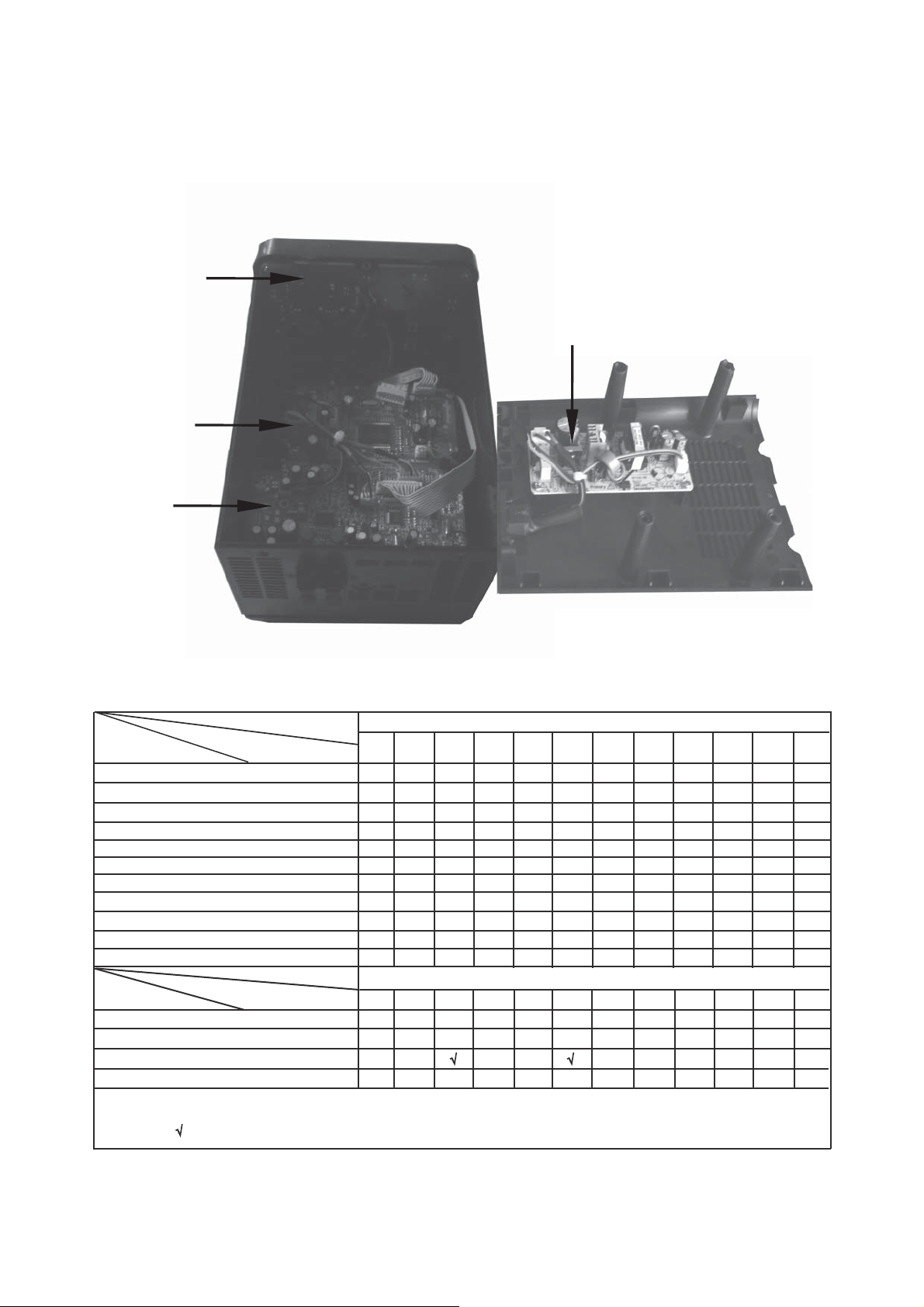
1.Location of PC Boards
Display Board
Decoder Board
AMP Board
Power Board
Version Variations
Type /Versions:
Board in used:
AMP Board
Decoder Board
Display Board
Power Board
Features
RDS
VOLTAGE SELECTOR
ECO STANDBY - DARK
DTS
* TIPS : C -- Component Lever Repair.
M -- Module Lever Repair
Service policy
Type /Versions
Feature diffrence
-- Used
/05
/05
MCM1050B
/55
/58
/61
/37
/12/10
CC
MM
CC
MM
/79
MCM1050B
/37
/12/10
/55
/58
/61
/79
/93
/93
/94
/94
/96
/96
/98
/98
1-1
Page 3
Technical Specification and Connection Facilities
2. General Information and Requirement
2.1 Product Family Features
2.1.1 Identity and Key Features
MCM1050 series are Micro Audio System with CD/MP3 player with USB and Tuner
FM(20presets)
Elements to include as generic requirements:
1. Detachable mains cord
2. Safety certification (cUL/FCC and CB/EMC/CE)
Following is a list of key features:
1. CD /MP3 disc player (Ali-M5673)
2. USB true source
a) MSC/MTP device
b) USB 2.0HS
3. MP3 Link (via headphones jack from PC or MP3 player)
4. Headphone Out (in front of the set)
5. Tuner FM(Silicon Lab SI4705/w RDS)
6. Digital Amplifier (ST class D,TDA7491HV)
7. Rated output power @10%THD table 2
Set Type Number Stroke Versions Power(ROP) Power(Volume max) Remark
MCM1050
All version 2x5W
2x12W
2.1.2 Styling, Forms and Functions
MCM1050 appearances are defined in their respective MUS. MUS is the leading document
where product appearance is applicable..
Features Products MCM1050
Stroke versions
Design
Optical Drive Loading Tray
Front
Dimension
Weight
Cosmetics
Tray Orientation HORIZONTAL
Apparatus tray closed
W x D x H (mm)
Refer to MUS[3] for
140x143x210mm
roloC
snottuB
llA
details
elddiM noitacoL yarT
PU DCL
mm3 teef fo thgieH
gk2.1 tes niaM
gk50.1 rekaeps
Black
Black
1-2
Page 4
Technical Specification and Connection Facilities
2.1.3 External I/O Connections
Model MCM1050
Stroke Version All
iPod dock with
Authentication chip
USB √
MP3 Link
(3.5mm audio jack)
Tuner Socket
(for FM)
Headphone Out
(3.5mm audio jack)
2.1.4 Controls, Local Display and LED Indications(tbc)
Control keys on the set are:
1. Standby-On
2. Eject
3. Play/Pause
4. Next
5. Pre
6. FF
7. FB
8. Source (Disc, USB, Dock, FM, Aux, MP3)
9. Stop
10. Volume Knob
There is local display LCD(reuse). Standby LED colour: Red in Standby mode.
2.1.5 ACCESSORIES (tbc)
Model MCM1055
Stroke Version All Version
eR
Power Cord
Audio cable
(3.5mm audio)
NA
√
√
√
noig
1.5M
0.5M
Remote Control
Quickly guide
IFU
31keys
1
1
1-3
Page 5
Technical Specification and Connection Facilities
2.2 Mechanical General Information
The product appearances and functions are defined in their respective MUS. Product management
approves the MUS and it is a leading document where product appearance is applicable.
Please refer to Sh560 for mechanical information.
Where applicable:
For /12 (EU), /05 (UK), /51 (Russia) EN/IEC 60065 7
For /37 (US, Canada) UL 60065
For /55 (LATAM), /78 (Brazil) IEC 60065 7
For /98 (AP), /69 (Singapore), /75 (Australia) IEC 60065 7
For /93 (China) GB 8898 (IEC 60065 7
For /61 (Korea) K 60065 6
For /96 (Taiwan) CNS 14408 (IEC 60065 7
Where applicable:
For /12 (EU), /05 (UK), /51 (R
For /37 (US, Canada) FCC15
For /55 (LATAM), /78 (Brazil) CISPR13
For /98 (AP), /69 (Singapore), /75 (Australia) CISPR13
For /61 (Korea) CISPR13/20
For /93 (China) GB 13837 (CISPR13)
For /96 (Taiwan) CNS 13439 (CISPR13)
Safety Standards
2.3
2.4
EMC Requirements
th
Edition
th
Edition
th
Edition
th
Edition
th
Edition)
th
Edition)
ussia) EN55013: 2001, EN55020: 2002
ESD Requirements
2.5
The product shall withstand electro static discharges on all user accessible parts of the product.
Reference: IEC61000-4-2.
For contact discharges:
Level General (kV) USA (kV) Requirement
1 0-2 0-3 No deviations allowed.
2 >2-4 >3-4 Short perceptible deviations allowed
3 >7-8 No loss of stored data allowed.
-
For air discharge:
Level General (kV) USA (kV) Requirement
1 0-4 0-6 No deviations allowed.
2 >4-8 >6-8 Short perceptible deviations allowed.
3 - >15-18 No loss of stored data allowed.
1-4
Page 6
Technical Specification and Connection Facilities
General requirement:
1. 10 arcs for positive and negative polarity for unit “on” and “off” for 1kV incremental steps.
2. Component or mechanical damage is not allowed. No loss of fixed stored data (stored in EEPROMs).
3. Hang-ups and malfunctions are allowed, as long as the customer can “recover” from the hang-up by
pressing the Standby or ON/OFF button of the set.
4. Failures that disappear only by unplugging the AC mains cord and/or power sources are not acceptable.
Environmental Condition
2.6
The environmental condition requirements and test method is according to UAN-D1590.
Ambient temperature : max. 40 ° C - all climates
Apparatus acc. to spec. : +5 to + 35 ° C
Vibration test (acc. IEC 60 068/2/6) : operational vibration test to be proceeded in operating position of the
set.
Quality
2.7
PQR-class: class 2 according to BLC A&MA PQR handbook V2.1 (2006-10-02)
Lifetime: 7 years
Tested According to: General Test Instruction UAN-D 1591
Measured According to: UAN_L 1059 unless otherwise stated
3. Technical Specifications
3.1 Power Supply
3.1.1 Type and versions
Build-inSMPS will be used for all models and stroke versions.
All using built in Power cord, will cater for all versions:
Versions Region/Country SMPS Detachable mains cords
12 / 05 EUROPE / UK
37 NAFTA
94 India
1) 100 ~240Vac nom. (wide
range from 90V~264Vac limit)
used in all versions except
India.
Frequency: 47~63Hz.
2) 100 ~310Vac limit (India
compatible with up cost) used
only for India.
Frequency: 47~63Hz.
EU (/12) round 2-pin & UK (/05) 3-pin
UL flat pin (non-polarized)
nip-2 dnuor UE CAPA 89
EU (/12) round 2-pin
nip-2 dnuor deifitrec ORTEMNI MATAL 55
All requirements per defined for each country should be met with sufficient testing.
1-5
Page 7

Technical Specification and Connection Facilities
3.1.2 Surge Immunity (Lightning Test)
The product shall withstand mains interference’s of:
Differential mode:
2kV/2 ohm criteria C for Europe.
6kV/12 ohm criteria C for NAFTA.
Parameters:
Bi-wave
Open circuit voltage: 2/50us
Short circuit current: 8/20us
From +/1kV to +/-2kV (for Europe) or +/-6kV (for Nafta) in steps of 1kV.
10 shots per combination.
One shot per minute.
Serial impedance: 2 Ohm for Europe, 12Ohm for Nafta.
Polarity and phase: Positive (phase 90º) & Negative (phase 270º)
Common mode:
6kV/2 ohm criteria C for Europe.
6kV/12 ohm criteria C for Nafta.
Parameters:
Ring-wave (100kHz)
From +/3kV to +/-6kV in steps of 1 kV.
10 shots per combination.
One shot per minute.
Serial impedance: 2 Ohm for Europe, 12Ohm for Nafta
Polarity and phase: Positive (phase 90º) & Negative (phase 270º)
Reference: IEC61000-4-5 and for USA: 3135 019 8029 Reliability evaluation.
Requirements:
Apparatus should fulfil the leakage current requirements of IEC60065 point 9.1.1 (UAN-D1631)
Defects or permanent deviations are not allowed.
3.1.3 Mains Drop-out Immunity
The product shall withstand mains failures of:
Variation 0% (=100% dip) at T-event = 50 mSec. Performance criterion B
Variation 40% (=60% dip) at T-event = 100 mSec. Performance criterion B
Variation 0% (=100% dip) at T-event = 5 Sec. Performance criterion C
Additional for USA apparatus: See 3135 019 8029 Reliability evaluation.
Variation 0% (=100% dip) at T-event = 100 mSec in standby mode. Performance criterion B
Requirement:
No misoperation and no interference of user in order to guarantee continuation of performed function.
Reference: IEC61000-4-11 For measuring method refer to UAN-D1724, as far as applicable.
Performance criterions according to IEC61000-4-4 Amendment 1
Performance Requirement
Criterion A - No any degradation of specification.
Criterion B - Temporary degradation / self recoverable.
Criterion C - No damage, resolvable hang-up.
Criterion D - Not recoverable loss of function.
1-6
Page 8
Technical Specification and Connection Facilities
x
3.1.4 Power Consumption
Power consumption at nominal AC input:
1. CD play mode at 1/8 P-rated output power
MCM1050: İ 20
W
2. Low Power Standby Mode : İ 0.5
W
3.2 Technical Description
traP larenreG
Output Stage Protection: NA Temperature : Yes Short Circuit: Yes
srotacidnI
evitcA yalpsiD kcolC :rotacidnI edoM ybdnatS
ffO snruT DEL :edoM ybdnatS rewoP
Electrical Data
DSC: Y(Flat/POP/JAZZ
/ROCK/CLASSIC)
DBB: Y(ON/OFF) Hum (Vol
Bass: NA -
Treble: NA Channel Seperation: 1kHz/10kHz 40dB/35dB
Signal to Noise Ratio(A-weighted): 77dBA 72dBA
Audio Inputputs
Audio Input Sensitivity(± 3dB) rated output power at 1kHz
Tuner FM 67.5kHz, Modulation (Limit:-6dB) Line Out(Left/Right) NA
MP3_link(front)
Output
Power(*1)
Main Operation for / all version (rms)
Tuner output power(rms)
Frequency Response(± 3dB)
Loudspeaker(Boxes): Separable speaker box Refer to package document of Speaker Box Assy
Speaker driver Impedance: Right/Left: 4Ω @ 40 Hz ~ 20kHz(-3db)
500mV ---- 1000mV; Rin ≥ 22kΩ
At THD=10%, 1kHz
sinewave
Channel Difference:
--- Vol
min
Amplification Reserve 3dB 2dB
MCM1050
(ROP,10%)
5W± 1dB
5W± 1dB
60Hz-20kHz
:refoowbuS
-20dB) 150nW -
ma
Audio Output(*1)
MCM1050
(Max Power,30%)
2X12W -1dB
NA
Normal
± 3dB
Limit
-
%0.1 %8.0 lamixaM,DHT AN :ssenduoL
Bd55 Bd06 :klatsorC
2 ± Wm51 enohpdaeH )1 kcarT ,1 csiD oiduA( kcart Bd3- 3PM/DC
dB, RL = 16Ω
)SH0.2 (evawenis zHK1 Bd3- BSU
REMARKS:
Electrical Parameters are to be measured at Speaker Terminals across rated impedance Load(4ohm) with
Rated Input Signal in CD Mode setting in DBB/Loudness Off and Pre-eq at Flat unless specified otherwise.
*--- measure max volume power with 1V MP3-link input
1-7
Page 9
Technical Specification and Connection Facilities
3.3 TUNER
FM use Silicon Lab Si4704/4705(w/RDS)
GENARAL PART
WAVE RANGE VERSION TOLERANCE TUNING GRID
FM 87.5 – 108.00 MHz /12 QUARTZ PRECISION 50kHz
FM 87.5 – 108.00 MHz /37 QUARTZ PRECISION 100kHz
AERIAL
FM : PIG TAIL ANT WIRE 75Ω
ELECTRICAL DATA
Frequency (MHz)
Units dBf DB dB mV/m dB
Susceptibility to unwanted signals(CPU,SMPS,AMP,DSP …):
Noise Limited
Sensitivity 26 dB
Search time digital tuning
system.
Overall Frequency Response: 63Hz –
12.5KHz
Channel separation:400 / 1000 / 5000 Hz.
RF input: 68 dBf
Image
Rejection
Limited(d
B)
-15dB -20dB Refer to selfpollution curve
IF Rejection
Normal
(dB)
Large Signal
Handling
fBd 62 02 tnioP gnitimiL Bd 3 -
14 53 )edom oerets ta(ytivitisneS gninuT hcraeS
- 60 S
Bd 15 84 gniteiuQ Bd 64 - oeretS
54 05 muH noitaludoM
54 05 oitaR N/S
Bd 4- 0 esreveR noitacifilpmA
% 3 2 ) zHk 57.veD qrF ,Vm1 FR ( noitrotsiD
- ±3 dB
26/30/
20
S9/300 kHz
Remark
Selectivity
22 0001 46 03 81.moN MF
22 0001 46 03 81.moN MF
54 fBd 611 06 03 81.moN MF
52 fBd 801 56 52 22.miL 0.701
20/26/
18
)1*( 81 005 54 52 22.miL 0.88
)1*( 81 005 54 52 22.miL 0.89
dB
tinU timiL moN MF
zHM 7.01 FI
1-8
Page 10
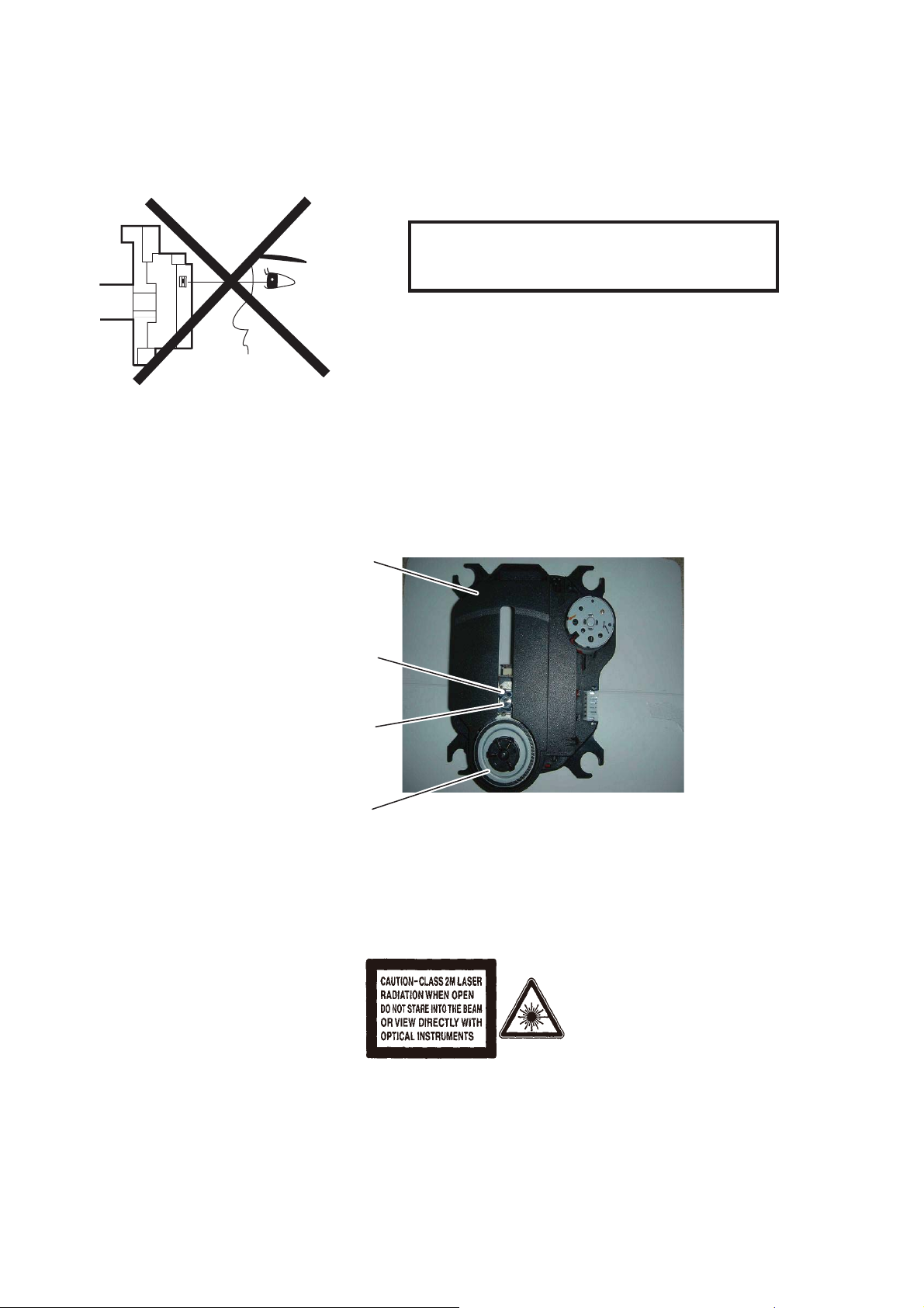
Laser Beam Safety Precautions
This Blu-Ray player uses a pickup that emits a laser beam.
Do not look directly at the laser beam coming
from the pickup or allow it to strike against your
skin.
The laser beam is emitted from the location shown in the figure. When checking the laser diode, be sure to keep
your eyes at least 30 cm away from the pickup lens when the diode is turned on. Do not look directly at the laser
beam.
CAUTION: Use of controls and adjustments, or doing procedures other than those specified herein, may result in
hazardous radiation exposure.
Drive Mechanism Assembly
Laser Beam Radiation
Laser Pickup
Turntable
Location: Inside Top of Blu-Ray mechanism.
2-1
Page 11

Important Safety Precautions
Caution: These servicing instructions are for use by qualified service personnel only.To reduce the risk
of electric shock do not perform any servicing other than that contained in the operating
instructions unless you are qualified to do so.
Important
Read and understand all instructions before you use
your home theater. If damage is caused by failure to
follow instructions, the warranty does not apply.
Safety
Riskof electricshock or fire!
Neverexposetheproductand
accessories to rain or water. Never place
liquid containers, such as vases, near the
product. If liquids are spilt on or into the
product, disconnect it from the power
outlet immediately. Contact Philips
Consumer Care to have the product
checked before use.
Never place the product and accessories
near naked
including direct sunlight.
Never insert objects into the ventilation
slots
or other openings on the product.
Where the mains plug or an appliance
coupler is used as the disconnect device,
the disconnect device shall remain readily
operable.
Disconnect the product from the power
outlet before lightning storms.
When you disconnect the power cord,
always pull the plug, never the cable.
Riskof short circuit or
Before you connect the product to the
poweroutlet,ensurethatthepower
voltage matches the value printed on the
back or bottom of the product. Never
connec
if the voltage is different.
Risk of injury or damage to the home theater!
For wall-mountable products, use only
the supplied wall mount bracket. Secure
the wall mount to a wall that can support
the combined weight of the product
and the wall mount. Koninklijke Philips
Electronics N.V. bears no responsibility
for improper wall mounting that results in
accident, injury or damage.
ames or other heat sources,
re!
ttheproducttothepoweroutlet
For speakers with stands, use only the
supplied stands. Secure the stands to
the speakers tightly. Place the assembled
stands on flat, level surfaces that can
support the combined weight of the
speaker and stand.
Never place the product or any objects
on power cords or on other electrical
equipment.
If the product is transported in
temperatures below 5°C, unpack the
product and wait u
matches room temperature before
connecting it to the power outlet.
Visible and invisible laser rad
open. Avoid exposure to beam.
Do not touch the disc optical lens inside
the disc compartment.
Risk of overheating!
Never install this product in a confined
space. Always leave a space of at least
four inches around the product for
ventilation. Ensure curtains or other
objects never cover the ventilation slots
on the product.
Risk of contamination!
Do not mix batteries (old and new or
carbon and alkaline,
Remove batteries if they are exhausted
or if the remote control is not to be used
for a long time.
Batteries contain chemical substances,
they should be disposed of properly.
ntil its temperature
iation when
etc.).
Product care
Do not insert any objects other than discs
into the disc compartment.
Do not insert warped or cracked discs
into the disc compartment.
Remove discs from the disc compartment
ifyouarenotusingtheproductforan
extended period of time.
Only use microfiber cloth to clean the
product.
3-1
Page 12

Important Safety Precautions
Disposal of your old product and
batteries
Your product is designed and manufactured
with high quality materials and components,
which can be recycled and reused.
When this crossed-out wheeled bin symbol
is attached to a product it means that the
product is covered by the European Directive
2002/96/EC.Pleaseinformyourselfaboutthe
local separate collection system for electrical
and electronic products.
Please act according to your local rules and
do not dispose of your old products with your
normal household waste.
Corr
ect disposal of your old product helps to
prevent potential negative consequences for
the environment and human hea
lth.
Your product contains batteries covered by
the European Directive 2006/66/EC, which
cannot be disposed with normal household
waste.
Please inform yourself about the local rules
on separate collection of batteries because
correct disposal helps to prevent negative
consequences for the environmental and
human health.
3-2
Page 13

Safety Check after Servicing
Examine the area surrounding the repaired location for damage or deterioration. Observe that screws, parts, and
wires have been returned to their original positions. Afterwards, do the following tests and confirm the specified
values to verify compliance with safety standards.
1. Clearance Distance
When replacing primary circuit components, confirm
specified clearance distance (d) and (d’) between
soldered terminals, and between term
surrounding metallic parts. (See Fig. 1)
Table 1: Ratings for selected area
inals and
Chassis or Secondary Conductor
Primary Circuit
AC Line Voltage Clearance Distance (d), (d
110V~220V
Note
: This table is unofficial and for reference only. Be
sure to confirm the precise values.
3.2 mm (0.126 inches)
’)
2. Leakage Current Test
Confirm the specified (or lower) leakage current
between B (earth ground, power cord plug prongs) and
externally exposed accessible parts (RF terminals,
antenna terminals, video and audio input and output
terminals, microphone jacks, earphone jacks, etc.) is
than or equal to the specified value in the table
lower
below.
Measuring Method (Power ON):
Insert load Z between B (earth ground, power cord plug
prongs) and exposed accessible parts. Use an AC
eter to measure across the terminals of load Z.
voltm
See Fig. 2 and the following table.
d' d
Fig. 1
Exposed Accessible Part
Z
AC Voltmeter
(High Impedance)
Earth Ground
B
Power Cord Plug Prongs
Table 2: Leakage current ratings for selected areas
AC Line Voltage Load Z Leakage Current (i) Earth Ground (B) to:
110V~220V
Note: This table is unofficial and for reference only. Be sure to confirm the precise values.
0.15 µF CAP. & 1.5 k
Connected in parallel
RES.
i
0.5 mA Peak Exposed accessible parts
4-1
Fig. 2
Page 14

Safety Information, General Notes & Lead Free Requirements
1 Safety Instructions
1.1 General Safety
Safety regulations require that during a repair:
Connect the unit to the mains via an isolation transformer.
Replace safety components, indicated by the symbol
only by components identical to the original ones. Any
other component substitution (other than original type)
Safety regulations require that after a repair, you must return
the unit in its original condition. Pay, in particular, attention to
the following points:
Route the wires/cables correctly
mounted cable clamps.
damage.
Check the electrical DC resistance between the mains
plug and the secondary side:
1. Unplug the mains cord, and connect a wire between
the two pins of the mains plug.
2. Set the mains switch to the ‘on’ position (keep the
mains cord unplugged!).
3. Measure the resistance value between the mains
plug and the front panel, controls, and chassis
bottom.
4. Repair or correct unit when the resistance
5. Verify this, before you return the unit to the customer/
user (ref. UL-standard no. 1492).
6. Switch the unit ‘off’, and remove the wire between the
two pins of the mains plug.
1.2 Laser Safety
This unit employs a laser
may remove the cover, or attempt to service this device (due
to possible eye injury).
2 Warnings
2.1 General
All ICs and many other semiconductors are susceptible to
,
during repair can reduce life drastically. Make sure that,
during repair, you are at the same potential as the mass
of the set by a wristband with resistance. Keep
components and tools at this same potential.
Available ESD protection equipment:
– Complete kit ESD3 (small tablemat, wristband,
4822 310 10671.
– Wristband tester 4822 344 13999.
Be careful during measurements in the live voltage
section. The primary side of the power supply, including
the heatsink, carries live mains voltage when you
connect the player to the mains (even when the
player is ‘off’!). It is possible to touch copper tracks and/
or components in this unshielded primary area, when
you service the player. Service personnel must take
precautions to prevent touching this area or components
in this area. A ‘lightning stroke’ and a stripe-marked
printing on the printed wiring board, indicate the primary
side of the power supply.
Never replace modules, or components, while the unit is
‘on’.
2.2 Laser
The use of optical instruments with this product, will
Only quali ed service personnel may remove the cover or
attempt to service this device, due to possible eye injury.
Repair handling should take place as much as possible
with a disc loaded inside the player.
T
shield:
electrostatic discharges (ESD,
). Careless handling
Laser Device Unit
epyT
:AIGalnN(BD)
:AIGalnP(DVD)
: AIGalnP(CD)
Wavelength : 650 nm (DVD)
)DC/DCV(mn087:
405nm(BD):
Output Power : 20 mW
)gnitirwWR+DVD(
Wm8.0:
)gnidaerDVD(
Wm3.0:
)gnidaerDC/DCV(
Beam divergence : 60 degree
CLASS 1
LASER PRODUCT
1-2erugiF
Note: Use of controls or adjustments or performance of
procedure other than those speci
ed herein, may result in
A
CAUTION VISIBLE AND INVISIBLE LASER RADIATION WHEN OPENAVOID EXPOSURE TO BEAM
ADVARSEL SYNLIG OG USYNLIG LASERSTRÅLING VED ÅBNING UNDGÅ UDSÆTTELSE FOR STRÅLING
ADVARSEL SYNLIG OG USYNLIG LASERSTRÅLING NÅR DEKSEL ÅPNES UNNGÅ EKSPONERING FOR STRÅLEN
VARNING SYNLIG OCH OSYNLIG LASERSTRÅLNING NÄR DENNA DEL ÄR ÖPPNAD BETRAKTA EJ STRÅLEN
VARO!AVATTAESSA OLET ALTTIINA NÄKYVÄLLE JA NÄKYMÄTTÖMÄLLE LASER SÄTEILYLLE. ÄLÄ KATSO SÄTEESEEN
VORSICHT SICHTBARE UND UNSICHTBARE LASERSTRAHLUNG WENNABDECKUNG GEÖFFNET NICHT DEM STRAHL AUSSETSEN
DANGER VISIBLE AND INVISIBLE LASER RADIATION WHEN OPENAVOID DIRECT EXPOSURE TO BEAM
ATTENTION RAYONNEMENT LASER VISIBLE ET INVISIBLE EN CAS D’OUVERTURE EXPOSITION DANGEREUSE AU FAISCEAU
Figure 2-2
5-1
Page 15

Standard Notes for Servicing, Lead Free Requirements & Handling Flat Pack IC
Circuit Board Indications
1. The output pin of the 3 pin Regulator ICs is
indicated as shown.
Top View
Out
2. For other ICs, pin 1 and every fifth pin are
indicated as shown.
Pin 1
3. The 1st pin of every male connector is indicated as
shown.
Pin 1
Input
In
Bottom View
5
10
Instructions for Connectors
1. When you connect or disconnect the FFC (Flexible
Foil Connector) cable, be sure to first disconnect
the AC cord.
2. FFC (Flexible Foil Connector) cable should be
inserted parallel into the connector, not at an
angle.
FFC Cable
Connector
CBA
* Be careful to avoid a short circuit.
Pb (Lead) Free Solder
When soldering, be sure to use the Pb free solder.
Information about lead-free soldering
Philips CE is producing lead-free sets from 1.1.2005
onwards.
IDENTIFICATION
Regardless of special logo (not always
indicated)
One must treat all sets from
onwards, according to the next rule:
Serial Number gives a 14-digit. Digit 5&6 shows the
YEAR, and digit 7&8 shows the WEEK.
So from onwards=from 1 Jan 2005 onwards
0501
Important note : In fact also products of year 2004
must be treated in this way as long as you avoid
mixing solder-alloys (leaded/ lead-free). So best to
always use SAC305 and the higher temperatures
belong to this.
Due to lead-free technology some rules have to be
respected by the workshop during a repair:
Use only lead-free solder alloy Philips SAC305 with
order code 0622 149 00106. If lead-free solderpaste is required, please contact the manufacturer
of your sol
paste within workshops should be avoided because
paste is not easy to store and to handle.
Use only adequate solder tools applicable for lead-
free solder alloy. The solder tool must be able
To reach at least a solder-temperature of 400°C,
To stabilize the adjusted temperature at the solder-
tip
To exchange solder-tips for different applications.
Adjust your solder tool so that a temperature around
360°C
solder joint. Heating-time of the solder-joint should
not exceed ~ 4 sec. Avoid temperatures above
400°C otherwise wear-out of tips will rise drastically
and flux-fluid will be destroyed. To avoid wear-out of
tips switch off un-used equipment, or reduce heat.
Mix of lead-free solder alloy / parts with leaded
solder alloy / parts is possible but PHILIPS
recommends strongly to avoid mixed solder alloy
types (leaded
If one cannot avoid or does not know whether
product is lead-free, clean carefully the solder-joint
from old solder alloy and re-solder with new solder
alloy (SAC305).
Use only original spare-parts listed in the ServiceManuals. Not listed standard-material (commodities)
has to be purchased at external companies.
der-equipment. In general use of solder-
- 380°C is reached and stabilized at the
and lead-free).
1 Jan 2005
6-1
Page 16

Standard Notes for Servicing, Lead Free Requirements & Handling Flat Pack IC
Special information for BGA-ICs:
- always use the 12nc-recognizable soldering
temperature profile of the specific BGA (for desoldering always use the lead-free temperature
profile, in case of doubt)
- lead free BGA-ICs will be delivered in so-called
'dry-packaging' (sealed pack including a silica gel
pack) to protect the IC against moisture. After
opening, dependent of MSL-level seen on indicatorlabel in the bag, the BGA-IC possibly still has to be
baked dry. (MSL=Moisture Sensit
will be communicated via AYS-website.
Donotre-useBGAsatall.
For sets produced before 1.1.2005 (except products
of 2004), containing leaded solder-alloy and
components, all needed spare-parts will be available
till the end of the service-period. For repair of such
sets nothing changes.
On our website
www.atyourservice.ce.Philips.com
information to:
BGA-de-/soldering (+ baking instructions)
Heating-profiles of BGAs and other ICs used in
Philips-sets
You will find this and more technical information within
the “magazine”, chapter “workshop news”.
For additional questions please contact your local
repair-helpdesk.
ivity Level). This
you find more
How to Remove / Install Flat Pack-IC
1. Removal
With Hot-Air Flat Pack-IC Desoldering Machine:
1. Prepare the hot-air flat pack-IC desoldering
machine, then apply hot air to the Flat Pack-IC
(about 5 to 6 seconds). (Fig. S-1-1)
Fig. S-1-1
2. Remove the flat pack-IC with tweezers while
applying the hot air.
3. Bottom of the flat pack-IC is fixed with glue to the
CBA; when removing entire flat pack-IC, first
soldering iron to center of the flat pack-IC and heat
up. Then remove (glue will be melted). (Fig. S-1-6)
4. Release the flat pack-IC from the CBA using
tweezers. (Fig. S-1-6)
apply
CAUTION:
1. The Flat Pack-IC shape may differ by models. Use
an appr
machine, whose shape matches that of the Flat
Pack-IC.
2. Do not supply hot air to the chip parts around the
flat pack-IC for over 6 seconds because damage
to the chip parts may occur. Put masking tape
around the flat pack-IC to protect other parts from
damage. (Fig. S-1-2)
opriate hot-air flat pack-IC desoldering
6-2
Page 17

Standard Notes for Servicing, Lead Free Requirements & Handling Flat Pack IC
3. The flat pack-IC on the CBA is affixed with glue, so
be careful not to break or damage the foil of each
pin or the solder lands under the IC when
removing it.
Hot-air
Flat Pack-IC
Desoldering
CBA
Masking
Tape
Machine
Flat Pack-IC
Tweezers
Fig. S-1-2
With Soldering Iron:
1. Using desoldering braid, remove the solder from
all pins of the flat pack-IC. When you use solder
flux which is applied to all pins of the flat pack-IC,
you can remove it easily. (Fig. S-1-3)
Flat Pack-IC
Desoldering Braid
4. Release the flat pack-IC from the CBA using
tweezers. (Fig. S-1-6)
With Iron Wire:
1. Using desoldering braid, remove
all pins of the flat pack-IC. When you use solder
flux which is applied to all pins of the flat pack-IC,
you can remove it easily. (Fig. S-1-3)
2. Affix the wire to a workbench or solid mounting
point, as shown in Fig. S-1-5.
3. While heating the pins using a fi
iron or hot air blower, pull up the wire as the solder
melts so as to lift the IC leads from the CBA
contact pads as shown in Fig. S-1-5.
4. Bottom of the
CBA; when removing entire flat pack-IC, first apply
soldering iron to center of the flat pack-IC and heat
up. Then remove (glue will be melted). (Fig. S-1-6)
5. Release the flat pack-IC from the CBA using
tweezers. (Fig. S-1-6)
Note: When using a soldering iron, care must be
taken to
being held by glue. When the flat pack-IC is
removed from the CBA, handle it
because it may be dama
flat pack-IC is fixed with glue to the
ensure that the flat pack-IC is not
the solder from
ne tip soldering
gently
ged if force is applied.
Hot Air Blower
Soldering Iron
Fig. S-1-3
2. Lift each lead of the flat pack-IC upward one by
one, using a sharp pin or wire to whic
not adhere (iron wire). When heating the pins, use
a fine tip soldering iron or a hot air de
machine. (Fig. S-1-4)
h solder will
soldering
Sharp
Pin
Fine Tip
Soldering Iron
3. Bottom of the flat pa
CBA; when removing entire flat pack-IC, first apply
soldering iron to center of the flat pack-IC and heat
up. Then remove (glue will be melted). (Fig. S-1-6)
ck-IC is fixed with glue to the
Fig. S-1-4
6-3
To Solid
Mounting Point
CBA
Tweezers
or
Iron Wire
Soldering Iron
Fig. S-1-5
Fine Tip
Soldering Iron
Flat Pack-IC
Fig. S-1-6
Page 18

Standard Notes for Servicing, Lead Free Requirements & Handling Flat Pack IC
2. Installation
1. Using desoldering braid, remove the solder from
the foil of each pin of the flat pack-IC on the CBA
so you can install a replacement flat pack-IC more
easily.
2. The “
(See Fig. S-1-7.) Be sure this mark matches the 1
on the PCB when positioning for installation. Then
presolder the four corners of the flat pack-IC. (See
Fig. S-1-8.)
3. Solder all pins of the flat pack-IC. Be sure that
none of the pins have solder bridges.
” mark on the flat pack-IC indicates pin 1.
Example :
Pin 1 of the Flat Pack-IC
is indicated by a " " mark.
Fig. S-1-7
Instructions for Handling Semiconductors
Electrostatic breakdown of the semi-conductors may
occur due to a potential difference caused by
electrostatic charge during unpacking or repair work.
1. Ground for Human Body
Be sure to wear a grounding band (1 M ) that is
properly grounded to remove any static electricity that
may be charged on the body.
2. Ground for Workbench
Be sure to place a conductive sheet or copper plate
with proper grounding (1 M
other surface, where the semi-conductors are to be
placed. Because the static electricity charge on
clothing will not escape through the body grounding
band, be
with your clothing.
careful to avoid contacting semi-conductors
<Incorrect>
) on the workbench or
CBA
Presolder
Flat Pack-IC
Fig. S-1-8
<Correct>
1M
CBA
Grounding Band
1M
CBA
Conductive Sheet or
Copper Plate
6-4
Page 19

FLOW CHART NO.1
No sound from whole unit
Troubleshooting
check if speaker is ok
check and change speaker and output wire
Yes
No
check if public circuit of whole unit
AMP circuit is ok
No
check radio tube and periphery circuit
Yes
check if power supply circuit of whole
unit is ok
No
check and change transormer of power supply and
power commutate circuit
Yes
check staic noisy circuit CPU circuit and change components
FLOW CHART NO.2
no sound from radio
check if output of radio is normal
No
check public circuit and circuit of power supply
Yes
No
check radio controlled circuit
check and change the related components of radio controlled circuit
Yes
check if power supply of radio is
normal
Yes
check if radio circuit an components
of around it is normal
FLOW CHART NO.3
no sound from CD
check if CD output is normal
No
Yes
check if CD controlled circuit is ok
Yes
check if the related components of CD
signal channel
tie wires socket is normal
No
check and change related components of power supply circuit
No
check and change components of around it
check public circuit
components
No
check and change the related components of CD
controlled circuit
check and change the related components of CD
No
tie wires
power supply circuit and change related
socket
Yes
change decoding board
9-1
Page 20

no search from CD
check if supply +12V of decoding board is normal
Yes
Troubleshooting
No
check steady circuit
check if laser head ass'y can light normally
No
check if tie wires of laser head ass'y
is loosen and broken
No
laser head ass'y broken
Yes
Yes
decoding board is broken
check and change good laser head ass'y
9-2
Page 21

MP3_Link
HP_OUT
MP3_LR_IN
5.6V
HEADSET DRIVER
PT2309
FL_OUT
TDA7491P
AMPLIFIER
STB/MUTE
FR_OUT
8OHM_5W*2
A3.3V
OPEN/CLOSEDRIVER
FM_LR_IN
DVD/CD_RL
D-/D+
IIC
MCU3.3V
9V
M3.3V
EEPROM
MCU
LCD BUS
Stb,clk data
BD3490FS
M3.3V
M24C02
CP2.0B
Apple Ceriticiate
R5F21266
IR
AD_KEY
STB/MUTE
TX/RX/CTL/DET
MCU3.3V
9V_BD3491/3490
VUSB_ON
DVD_ON
CD_5.6V
AMP JDA7491HV
9435
AP1501
DC/DC
12V/18V
CD/DVD_ON
GND
M3.3V
1117
5.6V
ECO
IGND
7333
LDO
I5V/3.3V
IPOD/IPHONE_5V
9.1V
ECO
10-1 10-1
M3.3V
si4705
FM(RDS)
A3.3V
FLASH
MX25L1605D
A3.3V
ALi5673
MAIN CHIPSET
CD_5.6V
RF
CD_5.6V
LOADER MOTOR DRIVER
AM5766
CD_5.6V
M3.3V
IR
Block Diagram
AS6622Q
LCD Controller
DA11
USB
WXD-8210D
(host 2.0)
LCD DISPLAY SCREEN
TRANSFORMER
AC220V
PSU BOARD
Page 22

CON4
AC220V
CON2
CON1
Power Board
PJ2
CON3
CON3
Decoder Board
J1
J3
CN1
J1
CON1
JP4
CON2
CON1
Display Board
Wiring Diagram
J7
PJ3
J6
AMP Board
J4
J2
CD Loader driver(machanism)
11-1 11-1
Page 23

Q1
8050
LED1
10K
470
22uF/10V
R20
3.3V
47R
R18
C8
100P
EC1
VCC
1
47uF/6.3V
GND
2
IR
REM
3
R14
10R
IR
SEG10
SEG09
SEG08
SEG07
SEG06
SEG05
SEG04
33
1
COM1
2
COM2
3
COM3
4
COM4
5
COM5
6
COM6
7
COM7
8
COM8
9
SEG1
10
SEG2
11
SEG3
12
SEG4
13
SEG5
14
SEG6
15
SEG7
16
SEG8
17
SEG9
LCD1
18
SEG10
19
SEG11
20
SEG12
21
SEG13
22
SEG14
23
SEG15
24
SEG16
25
SEG17
26
SEG18
27
SEG19
28
SEG20
29
SEG21
30
SEG22
31
SEG23
32
SEG24
COM00
COM01
COM02
COM03
COM04
COM05
COM06
COM07
COM[00:07]
SEG00
SEG01
SEG02
SEG03
SEG04
SEG05
SEG06
SEG07
SEG23
SEG22
SEG21
SEG20
SEG19
SEG18
SEG17
SEG16
SEG15
SEG14
SEG13
SEG12
SEG11
SEG10
SEG09
SEG08
SEG03
SEG02
SEG01
SEG00
SEG[00:23]
J8
R19
R31
47K
3.3V
SEG11
SEG12
SEG16
SEG13
SEG15
SEG14
13
12
SG11
SG16
SG15
SG14
SG13
SG12
11
SG10
10
SG9
9
SG8
8
SG7
7
SG6
6
SG5
5
SG4
4
SG3
3
SG2
2
SG1
1
DI
100R
R21
J3
J2
DATA
SG17
U1
OSC
VDDCECLK
VSS
R27
560R
100R
100R
102
R4
R3
J4
R29
J5
100P
100P
J1
CS
WR
EC4
10R
100uF/10V
R28
A5V
SEG19
SEG17
SEG18
SEG20
21
19
1817161514
20
SG21
SG19
SG18
SG20
I-PT6533
COM1
VLCD
COM2
COM3
COM01
COM02
COM00
C6
68K
C7
C11
EC5
22uF/10V
Q4
8050
R32
10K
82K
R33
5V
SEG21
22
SG22
SEG22
23
SG24
24
SEG23
SG25
25
SG26
26
SG27
27
SG28
28
SG29
29
COM8
COM07
30
COM7
31
COM06
COM6
COM05
32
COM5
COM04
33
COM4
3435363738394041424344
COM03
R7
240K
WR
R6
240K
A5V
J9
CS
R5
240K
LED2
150R
R22
A5V
C5
100P DATA
100P
C9
100P
C10
EC3
0
R24
8050
Q2
R25
100K
10K
R23
AD1
EC2
47K
2.2u/10V
R26
J7
J6
LED_PWM
R12
33K
SW5
ON/OFF
R11
20K
SW4
ON/OFF
R9
5.1K
SW2
ON/OFF
R8
470R
SW1
ON/OFF
R10
10K
SW3
J11
AD2
ON/OFF
R17
33K
SW9
ON/OFF
R16
10K
SW8
ON/OFF
R15
4.7K
SW7
ON/OFF
234
1
R13
470R
SW6
ON/OFF
SM4
SMARK
SM3
SMARK
SM2
SMARK
R30
120K
A5V
SM1
SMARK
Display Board -- Circuit Diagram
MP3_R
AUTO-OFF
AGND
1
321
CON1
2.0-3P
AGND
MP3_L
103
C2
47K
R2
103
C1
R1
47K
FB1
MP3_R
MP3_L
2
345
LRH
P
G
JP1
TE-03575
DDGND
DDGND
USB
DGND
GND
D+D-VBUS
D+
D-
ESD
Q3
2.0*5
CON2
12345
UVCC
121110
AUTO-OFF
GND
IR
AD1
WR
GND
CS
LED_PWM
DATA
987654321
5V
A5V
3.3V
AD2
D1
5819
DD
TP1
1
PJ4
CON12-2.0-AW
P5
P1
P2
P3
P4
DD
TP2
1
12-1 12-1
Page 24

Display Board -- Layout Diagram
12-2 12-2
Page 25

NC
C15
GND
NC
C14
9V
CON2
GND
9V
GND
9V
4
2
3
XH2.54-3PIN
1
R22
NC
R21
NC
C7
1000uF,10V
GND
GND
NC
3.3V
Q3
NC
Q2
C16
NC
NC
R23
NC
C18
IC3
NC
NC
R24
SOT23
NC
GND
GND
GND
D12
NC
HV
LT1
VIN
RT1
9V
UU9.8-30MH
D1
D2
2M,1206
JUMPER
1
2
1N4007
1N4007
2M,1206
C17
C19
R3
R2
104,275V
MOV1
103P,1KV
C1
47uF,400V
103/1KV
CX1
NC
2200uF,10V
GND
1nF,50V,0805
R26 22R,1206
2
L2
0R,0805
1 2
200K,1206
R1
200K,1206
R9
103P,630V
NC
L3
D11
7
4
NC
SW2
D7
C8
6
8
FR107
SW1
VCC
NC
R14
5.1R,0805
D6
FR107
GND GND
HGND
9VA
C4
221P,2KV
Q1
4N60
DRV2
R13
68R,0805
DRV1
R25
330R,0805
FB
R11
D5
NC
R29
9V
IC1
PC817
C11
HGND
10K,0805
NC
IC4
R20
R16
3.3K,0805
470pF,0805
CS1
CS2
4
CS
SOT23-6
KB8235
OUT
6
R18
5.1K,1%,0805
R17
NC
C13
10K,0805
C12
0.1uF,0805
HGND
R10
1.2R,1206
R8
NC
NC
R7
1.2R,1206
R6
R12
1K,0805
C9
470pF,0805
FB
R15
100K,1%,0805
3
2
1
FB
RT
GND
VCC
5
C10
12K
R19
2.32K,1%,0805
IC2
TL431A-0.5%
SOT23
HGND
HGND HGND HGND
HGND
HGNDHGND
NC
GND
GND
GND
HGND
GND
2200P,400V
CY1
HGND
12-3 12-3
L1
2.2uH,3*15mm
C6
9VA
HGND
9V 4A
D9
SB3100
HV
D8
T1
SB3100
EE22
C21
R35 22R,1206
10
1
C3
R28
GND
4
3
D4
1N4007
D3
1N4007
R5
2M,1206
R4
2M,1206
F1
T2AL250V
2PIN
CON1A
3
2
1
Power Board -- Circuit Diagram
22uF,50V
HV
R33
1M,1206
R27
1M,1206
C2
HGND
Page 26

Power Board -- Layout Diagram
12-4 12-4
Page 27

P1
WP4-3
324
1
L0603B
R_OUT
220uF/35V
CD11X/220UF16V/D6.3H7
CD11X/10UF16V/D4H7
0.1uF
+
CE2 10UF/16V
CB10 33PF
U2
1A12A23B14B25C16C27D18D29
33PF
33PF
33PF
33PF
L1 FB/1K
C9 4.7uF
R5
22K
C4
680pF
R4
22K
C3
680pF
1uF
C7
L_FM
R_FM
R47
20NC19
18
17
16
15
14
13
DFS
LOUT
DOUT
GPIO1
IRQ/GPIO2
GND
DCLK/GPIO3
FMI3RFGND4TXO5RST6SEN7SCLK8SDIO9RCLK10VIO
1NC2
FMRST
10K
100pF
R6
C33
100pF
100R
C22
R87
100R
FM_RST
R63
MSCL
L_OUT
C-0603
R25 3K
2.2UFC-0603
+
L7 FB/1K
C19 4.7uF
22K
680pF
22K
C17
FM_IN_R
R16 0R
R15 1K
23
OUT1
L9 FB/1K
C20 4.7uF
680pF
4700pF
C26
R18 NC
R20 0R
21SR22
20
SB2
SB1
SEL210SEL111VOL112VOL213TC214TC1
C25 2.2uF
L11 FB/1K
CB11 33PF
C24 4.7uF
R19 1K
FM_IN_L
C21
R28
22pF
C11
C23
DETECT
GND
GND
AUTO-OFF
1234567891011
R29 3K
2.2UF
CE4
+
33pF
0.22uF
0.22uF
0.22uF
0.22uF
L12 FB/1K
CB13
CB16
CB17
CB19
CB18
15
BCB216BCA217BCA118BCB119OUT2
BD3490
BD3490FV
BD3490FV
3300pF
C32
C27 2.2uF
C31
3300pF
CB15 33PF
CB14 33PF
CB12 33PF
C-0603
470pF
C36
470pF
C29
47K
R33
470pF
C35
47K
R23
C28
470pF
R32
47K
R31 1K
R30 1K
47K
R22
R21 1K
AL
AR
FM_IN_R
C30
0.1uF
1u
0R
C12
1uF
C8
104
GND
A
Y1
32.768KHz
22pF
4.7R
R34
D_5V
TP1.5-TOP
LCD_5V
LCD_5V
AD1
LCD_DATA
LCD_WR
LED_PWM
REMOTE
LCD_CS
AD2
MCU3_3V
GND
LO
RO
HP_MUTE
LCD_5V
LED_PWM
GND
LCD_DATA
LCD_CS
AD2
MCU3_3V
LCD_WR
AD1
REMOTE
12
J4
CON12
L15
U4
10K
R158
AD1
AD2
IPOD_ACCDET
IPOD_AUDIO_DET
AUTO-OFF
STBY
IPOD_CHARGE
100R
TP-CTC
330R
47K
R161
MCU3_3V
10K
R37 10K
MCU3_3V
C39
LO
1000pF
220uF/16V
+
CE7
220uF/16V
47uF/16V
47uF/16V
+
+
CE9
CE6
C37 0.1uF
5
6
7
8
IN2
VDD
BIAS
OUT2
OUT12MUTE3IN14GND
1
R35 10K
+
CE8
47uF/16V
R36 100k
HP_MUTE
12
+
220uF/16V
CE5
D2 1N4148
R41 47k
1000pF
C38
RO
MUTE1
R_OUT
CE3
MSCL
MSDA
R11 1K
R8 1K
L8 FB/1K
24
VCC26SDA27GND28FIL25SCL
L4 FB/1K
L5 FB/1K
L3 FB/1K
L2 FB/1K
C13 4.7uF
C10 4.7uF
C15 4.7uF
C16 4.7uF
R13
C18
R12
R7 4.7K
R10 4.7K
IPOD_L
IPOD_R
FM_IN_L
1uF
C14
M3_3V
10R
R26
4.7R
12
11
VDD
GND
ROUT
R65
U1
SI4702
GND
A
100R
R27
MSDA
MP3_R
MP3_L
123
J3
CON1
R-0805
R1
10R
8V
A
CE1
+
CB9
CB8
CB4
33PF
CB7
CB3
33PF
CB6
CB2
33PF
CB5
CB1
33PF
R3 1K
R2 1K
C1
4.7uF
C-0603
C2 4.7uF
MP3_L
MP3_R
A
GND
R9
0R
A
GND
PJ3
AV2-8.4-9
231
11223
3
J6
TP37
TP38
TP39
PJ2-A
JP-CK3511
1
3
11
2
10
GND
CD_5V
123
J1
CON1
TP14
CD_5V
J2
CON5
M3_3V
GND
100p
100p
C5
C6
FB4
FB/100R
FB3
FB/100R
PJ2-B
ALARGND
CD/DVD_MUTE
SSCL
SSDA
12345
6
AL
AR
TP33
SSCL
SSDA
CD/DVD_MUTE
21
GND
10K
R83
104
C40
270nH
FMRST
FB6
TP1.5-TOP
GND1
RO
LO
HP_MUTE
HP_MUTE
FLO-
FRO-
FLO+
FRO+
FLO+
FLO-
FRO-
FRO+TP1.5-TOP
0.1UF
C46
C45
100pF
C44
8.2R
0.22uF
R56
C50
15UH
L14
R57
20R
C43
100pF
1uF
100R/6A/100M
GND
SUB_GND22INPA23INNA27SGND26VDDS28DIAG19VDDPW18PGND25SYNCLK24ROSC30GAIN031GAIN135SVCC
1
GND
C41 4.7uF
5.6k
R55
R_OUT
R53 100
R52 100
R51 1K
R50 100R
R49 100R
R24
R160
R40 10K
R39 10K
IPOD_RX
R38 10K
R17
R46 10K
R45 10K
REM
R44 10K
MSCL
R43 68K
MSDA
R42 4.7K
L_OUT
R48 47k
+
CE10
U3
PT2309 SO8
+
CE11
47uF/16V
Q1
2N3904
13
2
R58
R54 4.7K
HP_LINE_MUTE
C54
C53
C52
C51
R59
68K
R149
IPOD_CHARGE
MUTE_PH_LINE
LED_PWM
IPOD_TX
47K
C57
C56
C55
GND
0.47UF
C48
C49 0.1uF
0.1UF
100pF
0.22uF
C58
330P
C62
100pF
L20
VDDS
DIAG
L18
FB/1K
FB-0603
C-0603
C61
0.1uF
1000pF
1uF
1000pF
1500PF
2.2k
C60 104
C59 104
MCU3_3V
8.2R
R60
R71 8.2R
15UH
15UH
L13
L10
GND
C67
100pF
L24
100R/6A/100M
100R/6A/100M
2
OUTPB
C66
0.1uF
22R
100k
R61
R64
L21
FB/1K
FB-0603
VDDS
SSDA
R68 100R
L23FB/0603/2.2K
24
SSDA
AD_KEY
25
FM_RST
26
CLOSE_M
27
RTC_IN
28
OPEN_M
29
CLOSE_SW
30
OPEN_SW
31
TRIN
32
SSCL2DVD_ON3RESET4P4_75AVSS6P4_67VCC8MODE
1
L22
FB/0603/2.2K
R69 1K
R66 100R
SSCL
CD/DVD_ON
R62
4.7K
MUTE1
4.7K
R67
D4
1N4148
D3
1N4148
CD/DVD_MUTE
LCD_WR
R70 100R
L26FB/0603/2.2K
+
0.1UF
C70
C69
100pF
C68
0.22uF
R73
20R
R75 0R
LCD_CS
R74 100R
L27FB/0603/2.2K
22
VFD_STB23VFD_CLK
J7
4P_1.0UP
1u/50V
CE12
R72
68K
D6
D5
MCU_MUTE
C76
R76 100R
L29FB/0603/2.2K
123
1N4148
1N4148
C75
C74
C73
LCD_DATA
21
U5
L30 DCR33R
M3V3
TP1.5-TOP
GND
0.47UF
1uF
0.1uF
R78 0R
0.1uF
R77
VFD_DATA
R5F21266
GND2
TP1.5-TOP
C82
0.22uF
C79
C80
GND
L31 FB/1K
C78
0.1uF
39K
C77
1500PF
2.2k
R80
MCU3_3V
R79 33R
R81 100R
20
VREF
R5F21266-LQFP32
4
MODE
RESET
TP1.5-TOP
TP1.5-TOP
HP_LINE_MUTE
MUTE_PH_LINE
0.1UF
C81
100pF
R82 8.2R
15UH
L6
330P
C87
L35
100R/6A/100M
8
9
OUTNB4PGNDB5PGNDB6PVCCB7PVCCB3OUTPB11OUTNA10OUTNA13PVCCA12PVCCA14PGNDA17OUTPA16OUTPA15PGNDA
OUTNB
VSS32INPB33INNB21MUTE20STBY
36
L33 FB/1K
C85 4.7uF
5.6k
R85
L_OUT
IPOD_TX
REMOTE
R84 100
REM
17TX18
19
REMOTE
ECO_POWER
L32 DCR33R
D7
1N4148
GND
100pF
C92
34
29
SVR
VREF
R89 30k
C91
1000pF
C90
1uF
C89
1000pF
MCU3_3V
IPOD_DET
R88 10K
R86 4.7K
RX
16
STANDBY
15
MSCL
14
MSDA
13
MUTE
12
LED_CTRL
11
ROTB
10
ROTA
9
X1
32.768kHz
R90
MCU3_3V
10u/10V
GND
D8
10K
+
CE13
C94
10u/10V
37
TDA7491P
TDA7491HV
C98
C97
R91
30K
C96
C95
REST
1N4148
12
C93
0.1uF
220uF/16V
3.3R
R106
0.01UF
C103
0.1uF
C102
GND
8V_IN
EC3
1000U/35V
GND
2.2UF
2.2u
BS3904
Q2
32
1
C101
0.1uF
R107 100
22k
R105
R95 10k
R93 10k
MCU3_3V
L37 FB/0603/2.2K
L36 FB/0603/2.2K
15PF
15PF
D9
C99
STBY
R104 3.3k
MUTE1
IPOD_RX
R94 100
ECO_POWER
R103 100
MSCL
R102 100R
MSDA
R101 100R
MCU_MUTE
R100 100R
FM_RST
R99 100R
LED_PWM
R98 100R
MUTE_PH_LINE
R92 100
SSDA
C109 100pF
SSCL
C108 100pF
LCD_CS
C107 100pF
LCD_DATA
C106 10pF
MSDA
C105 100pF
MSCL
C104 100pF
ESD
0.01UF
1A02A13A24
GND
24C02
SDA6SCL7TEST8VDD
5
0.1uF
C100
R97 330R
R96 330R
L39 FB
MSDA
MSCL
M3_3V
MUTE1
BAS316
D20
R159
1K
Q9
8550
CE15
+
M3_3V
C110
47uF/16V
CAP-4X7MM
0.1uF
2.2uF
C111
100K
R110
MP3_L
D1
BAS316
R115
NC
NC
R114
NC16
16
NC17
17
NC18
18
NC19
19
NC20
20
VSS1
21
AUTO-OFF
D10
C113 1uF
R111
100K
R113
C112 2.2uF
100K
R112
MP3_R
C34
10UF
1
MSDA
MSCL
R123 NC/330R
R120 NC/330R
R119 NC/10K
14
15
NC15
MODE0
iPod_CP_2.0
NC/KITMFI341S2164 QFN20
NC12MODE13NC34NRESET5VCC
1
NC/0R
R118 10K
R122
FM_RST
M3_3V
+
CE16
47uF/16V
R117
100K
BAS316
BAS316
D11
R116
100K
R121
VCC11
8
7
7
6
6
5
5
47K
CF4558
2
11
12
VSS
NC10
10
I2C_SCL13I2C_SDA
NC9
9
NC8
8
NC7
7
NC6
6
CB21 0.1uF
CB20
0.1uF
+
CE17
47uF/16V
R124 NC/0/0805
M3_3V
IPOD_AUDIO_DET
+
CE18
47uF/16V/NC
R134
D12
BAS316
100K/NC
D13
BAS316
R131
R125 47K/NC
100K/NC
10K/NC
C116 1uF/NC
2
2
3
3
VSS
4
100K/NC
R130
C114 2.2uF/NC
C115 2.2uF/NC
100K/NC
100K/NC
R127
R129
R_IPOD_BT
L_IPOD_BT
C118 33PF/NC
IPOD_R
IPOD_L
C117
33PF/NC
10K/NC
R133
TP22
10K/NC
R132
IPOD_RX
IPOD_DET
IPOD_TX
IPOD_L
L42 0/NC
R126 FB1K/NC
IPOD_R
R128 FB1K/NC
TP1.5-TOP
TP26
IPOD_ACCDET
IPOD_TX
IPOD_RX
IPOD_ACCDET
A
L_IPOD_BT
R_IPOD_BT
1
L43 0R/NC
IPOD_DET
8765432
CON1
CON8-FFC-90
12-5 12-5
8V_IN
8V_IN
R109
10K
R108
AMP Board -- Circuit Diagram 1
Page 28

U9
SOP8-P
IP5V
100R/5A
L46
IPOD_5V
22UH
L45
AP1534/SOP-8
VCC
4
100R/5A
L44
CD/DVD_ON
CE22
+
FB
OCSET
C128
0.1uF
10u/10V
VSS
VSS
EN
DRBOM
+
R144
220u/10V
R143
8
7
2
0.1uF
CE23
1K
1.2K
D15
SK34
0
R145
ECO_POWER
220u/25V
8V_IN
TP30
C129
MCU3_3
10K
R146
1
Q4
0.1uF
R147
32
BS3904
R148
22R
22K
NC
R14
MCU3_3V/IP5V
U11
LCD_5V
100R/5A
FB2
SOT89
NC/HT7333
MCU3_3 V
3
2
100R/5A
L51
OUT1
IN
D_5V
100R/5A
FB5
ECO_POWER
CE26
100u/10V
+
M3_3V
C131
0.1uF
Q5
8550
47K
R150
0.1uF
C130
+
CE25
100u/10V
GND
1
+
CE24
100u/16V/NC
10K
R152
22K
R153
1
32
R151
1K
Q6
BS3904
A8V
R155
1K
32
BS3904
8550
100R/5A
L52
Q7
Q8
1
47K
R154
220u/25V
CE27
+
R157
10K
R156
ECO_POWER
22K
12-6 12-6
CE21
100u/10V
D_5V
+
C
SOT-23-A
Q3
1
LPM9017
23
47K
U10
SOP8-P
8V_IN
100R/5A
FB1
5V
22UH
L49
AP1534/SOP-8
VCC
4
100R/5A
L48
R142
C127
C126
R141
6.8K
C125
NS/100nF
1
5
O/P6O/P
3
NS/100nF
C124
R140
4.7K
IGND
J8
3
11223
A
GND
100R/5A
TP-CTC
L16
0.1uF
C121
+
R136
6.8K
C120
153
1
5
FB
O/P6O/P
VSS
VSS
EN
OCSET
3
NS/100nF
C119
4.7K
R135
C122
+
CE19
0.1uF
220u/10V
R137
8
7
2
DRBOM
CE20
1.2K
D14
SK34
0
R138
IPOD_CHARGE
GNDGND
220u/25V
A
GND
R139
22R
A
GND
A
A
GND GND
GND
A
C123
0.1uF
A
A
AMP Board -- Circuit Diagram 2
GND
8V_IN
11223
MCU3_3V/IP5V
3
CON3
Page 29

AMP Board -- Layout Diagram
12-7 12-7
Page 30

VREF_16
CD_TRIN
R73 33
1
CON1
CON2.0-6
SPIN+1SPIN-
SLED-4LIMIT1
LIMIT2
SLED+
2
5
6
LRCK
73
70
74
72
71
75
XGPIOD7/SPDIF
XGPIOD6/I2S_WCLK
XGPIOE3/SD_MS_WP
XGPIOE1/DOCD_DATI(I)
XGPIOE2/DOCD_CLK(O)
XGPIOE0/DOCD_DATO(O)
XPAD_BICAFL
XPAD_LINEOUTL
XAVSS33_CKG
XAVDD18_1
XPAD_BOCAPL
XAVSS18_1
32
30
31
33
28
29
C26
0.1UF/NC
C26
0.1UF/NC
104
CD_L
C25
RF_1V8
Y1
16.9344MHz
30pF
R24
100k
C27
TP5
SCLK
MCLK
SDATA
68
67
69
66
XGPIOD5/I2S_DI
XGPIOD4/I2S_DO
XGPIOD2/I2S_SCLK
XGPIOD3/I2S_REFCLK
XPAD_LINEOUTR
XPAD_BICAPR
XAVSS33_AUD
XPAD_BOCAPR
35
36
34
37
C28
0.1UF/NC
C28
0.1UF/NC
CD_R
TP6
TP4
3
SL+
SPIN+
SPIN-
LIMIT
SL-
TP7
TP8
TP9
TP12
TP10
TP11
SPIN-
104
C31
SPIN+
SSDA
3V3SD
R25 330RR25 330R
65
XGPIOD1/I2CM_DAT(B)
XAVDD33_AUD
38
C32
104
EC11
10uF/16V
AUD_3V3
C30
102
102
C29
CN1
R26 4.7KR26 4.7K
SF-P200Z(FPC)
1
3.3Ω
L2
2
HAVC
1
2
VC
RX
TX
XGPIOD0/I2CM_CLK(O)
XGPIOC3/URRX
XGPIOC2/URTX
XGPIOC1/SFSCK
XGPIOC0/SFCSB
XGPIOB7/SFDI
XGPIOB6/SFDO
VDD_PAD
GND_PAD
GND_CORE
VDD_CORE
XDP
XDM
XPAD_SFGN
XPAD_SFGP
XPAD_XVREF
XPAD_V15R
XPAD_V08R
XPAD_V15L
XPAD_V08L
XPAD_MICBIAS
XPAD_LINEINL
FMINL
XPAD_MICIN
XPAD_LINEINR
FMINR
3V3SD
EC12
C33
MAPUH
MDPUH
TNI
R27 33K
3
4
E
D
VCC
R28 4.7KR28 4.7K
64
63
62
61
60
59
58
57
56
55
54
53
52
51
50
49
48
47
46
45
44
43
42
41
40
39
220uF/16V
104
MBPUH
6
A5B
V18
GNDM-OPEN_SW
CLOSE_SW
TP16
TP15
3V3SD
SSCL
330R
R31
TPI
MCPUH
R29 33K
8
7
F
C
RF_1V8
L3 DCR33
M+
TP18
TP17
10K
R30
R32 10K
RX
TX
LD
10
9
LD
GND
SEV_3V3
1
2
CON3
CON2.0-4
C35
104
EC18
100uF/16V
USB5V
F1
2
D4
1N5819
1
+5.6V
AUD_3V3
DCR33
L7
D6
NC
D5
NC
SPIN-
22K
R45
10K
SMD0805P100TF 1A 6V
R42
R44 1.5K
EC19
10uF/16V
104
C36
R41 NC/0R
AUD_3V3
3V3SD_IC
DCR33
L8
SPIN+
10K
R47
1
234
TX
M33V
V18_CORE
C34
104
DCR33
DCR33
L6
L4
M33V
CON2
CON2.0-5
12345
TP19
4
3
D+
L5 DCR33
Ferrite Bead 500mA
TP22
F_CS
F_DI
F_DO
F_CLK
TP21
TP20
33R
33R
R37
R38
R35
15k
M33V_PAD
R34
15k
V18_CORE
EC14
10uF/16V
EC17
10uF/16V
EC16
10uF/16V
EC13
10uF/16V
FOCUS-
TRACK+
MDI
FOCUS+
TRACK-
14
13
11
15
16
12
T-
F-
F+
T+
VR
MD
M33V_PAD
C42
CD_MUTE
LIMIT
CD_TRIN
C41
DCR33
L9
R51 4.7K(NC)
R54 4.7K(NC)
R53 10K
M33V
3V3SD
CD_R1
CD_L1
474
474
C133
C143
CD_L
CD_R
R49 27K
1.5K
R48
R56
100K
3V3SD
C40
104
8
VCC
CS#1DO
R55
100K
F_CS
2
3
2
3
HOLE/GND
H2
9
8
9
8
2
3
2
3
HOLE/GND
CON4
CON2.0-4
H1
8
9
8
9
104
C38
104
104
+5V
F_DO
F_CLK
6
5
7
CLK
HOLD#
WP#3GND
4
2
WP
GND
F_DI HOLD#
5
445
6
7
6
7
5
4
5
4
7
6
7
6
M33V_CKG
C43
104
DCR33
L10
R57 220R
+3.3V
C44
+5V
D7
1 2
+5.6V
DI
U3
SFLASH EON25P20(1M bit)
1
1
1
1
M33V_LDO
3V3SD
C46
104
DCR33
DCR33
L11
L12
CDR 2
CDL 2
A
C51
2200P
CDR
CDL
R67
10K
D8
3.3V/SMD
1uF/50V
2R2
R58
IN4001
U4
+3.3V
HOLE/GND
H4
2200P
C50
10K
R66
R64 10K
R63 10K
+
+
22UF/6.3V/4*7
CE2
CD_R1
CD_L1
C52
2.2uF
C49
2.2uF
A
A
2
C45 2.2uF
11
10
13
14
9
8
12
L13 DCR33
1
VA
GND
FLYP
FLYN
-VFILT
AOUTB
AOUTA
CS4354
CE4354
VL
MCLK3LRCK
GND6FILT+
SDIN
SCLK/DEM
5
1
4
7
2
2.2uF
C48
C47
0.1uF
R65
10K
R60 22R
R61 22R
R59 22R
R62 22R
LRCK
MCLK
SDATA
SCLK
CD_MUTE
220uF/10V
EC15
+5.6V
CD_5V
SSDA
C53
104
SSCL
R72 33R
1
2
5
3
4
J2
CON5
2
4
5
5
2
334
1
1
8
9
776
8
9
6
MK1MK1
MK2MK2
12-8 12-8
VREF_16
XSLEGP
EC1
VREF_16
10uF/16V
C1
104
TRACK
R1 51k
2
J3
CON3
MUTE34
C4
V18_CORE
3V3SD_IC
C3
SEV_3V3
C2
TRACK+
SPIN-
XSPINDLE
XTRACK
SPIN+
TRACK-
VREF_16
0R
474
C8
R2
R5 1K
C5 103
15
SPINDLE
+5.6V1
16
17
3.9K
18
19
R9 560K/0
R4
20
21
R8
82K/39K
22
23
24
25
26
27
28
C6
104
MUTE34
C7
104
+5.6V1
EC2
1000uF/10V
R3 2.2R
+5.6V
R11
3V3SD
CD_MUTE
LIMIT
CD_TRIN
R7
4.7K
R6
10K/NC
103
104
105
106
107
108
109
110
111
M33V_PAD
112
VREF_16
XSLEGP
XSPINDLE
XFOCUS
XTRACK
113
114
115
116
117
118
119
120
FMO
121
122
DMO
123
124
125
FOO
126
TRO
127
MDI
128
MDI
3V3SD
2
DCR33
L1
1
EC5
R10
15R
104
104
104
VOTKVOLD+
VOLDVCC2
OPIN
VCTL
GND29GND
GND
VINLD
OPOUT
TRB_2
VINTK
BIAS
MUTE
U2
AM5766FM
EC4
10uF/16V
2
4.7K
3
Q2
102
XGPIOI2/IRC
XGPIOI3
XGPIOI4
XGPIOI5
XGPIOI6
XGPIOI7
XGPIOJ0
XGPIOJ1
XGPIOJ2
GND_PAD
VDD_PAD
GND_CORE
VDD_CORE
XAVDD_D33
BTN_ADIN1
BTN_ADIN2
BTN_ADIN3
VREF16
XAVD33_1
XAVSS33_1
GPWM
1
LDO
47uF/16V
2
13
Q1
D1
12
VOFC+14VOTK+
VOFC-
13
VOSL-
12
VOSL+
11
VOTR+
10
VOTR-
9
VCC1
8
30
REV
7
FWD
6
REGO1
5
VINSL+
4
REGO2
3
TRB_1
2
VINFC
1
+5.6V
R13
47K
1 2
D2
1N4148
1
2N3904
1K
R12
RESETJ
96
97
99
100
101
98
XPRSTB
XGPIOH5/LCDA0(O)
XGPIOI1/PWM0_0(O)
XGPIOI0/LCDWRJ(O)
XGPIOH6/LCDCSJ(O)
XGPIOH7/LCDRDJ(O)
MB
LDO
TP2
MC
MD
5
2
3
4
6
MCPUH
TNI
TPIRXMAPUH
MBPUH
MDPUH
SEV_3V3
8550,DIP
1N4148
LD
FOCUS+
FOCUS-
SL+
SL-
+5.6V1
R14
10R/0.5W
D3
ESD
C10
105
94
91
93
95
92
XGPIOH1/DATA4(B)
XGPIOH3/DATA6(B)
XGPIOH2/DATA5(B)
XGPIOH4/DATA7(B)
XGPIOH0/DATA3(B)
XGPIOG7/DATA2(B)
V12
XAVDD33_2
XAVSS33_2
MA7TP1
TELP
HAVC
8
9
10
12
11
C12 104
104
C9
C13
EC6
C11
104
EC7
HAVC
10uF/10V
2
1
Q3
8550,DIP
3V3SD
R15 10K
87
86
88
89
90
XGPIOG3/USI_DI
XGPIOG2/USI_DO
XGPIOG4/USI_CLK
XGPIOG5/DATA0(B)
XGPIOG6/DATA1(B)
MPXOUT2
COSP
MPXOUT1
COSN
MPXOUT3
15
14
16
13
17
SBLPFO
C14 105
TELPFO
FELPFO
SB
TE
SEV_3V3
FE
104
10uF/10V
473
C18
R19 0R
3.3K
R18
R17 15K
SLEGP
20K
R16
3
M33V
M33V_PAD
104
C17
82
83
85
84
VDD_PAD
GND_PAD
XGPIOF3/SD_MS_DET
U1
U1
VTB
VTP20XTALI
XAVDD33_3
18
21
19
104
C15
EC8
C16 104
XGPIOF2/SD_MS_PWR
XAVSS33_3
M33V_LDO
R20
12K
C19
EC9
470uF/10V
C22
104
81
80
XGPIOF1/SD/MS_CLK(O)
XGPIOF0/SDCMD(B)/MSBS(O)
XAVSS33_LDO
XAVDD33_LDO
23
22
V18
C20 104
10uF/10V
VREF_16
XFOCUS
0R
103
R23
C24
R22 43k
FOCUS
104
77
76
79
78
XGPIOE5/SDD1(B)
XGPIOE4/SDD0(B)
XGPIOE7/SDD3(B)
XGPIOE6/SDD2(B)
ALi M5673
ALi M5673
XAVDD33_CKG
XAVDD18_LDO
XTALO
26
24
25
27
M33V_CKG
EC10
1000uF/10V
0R
R21
104
C21
C23 30pF
Decoder Board -- Circuit Diagram
Page 31

Decoder Board -- Layout Diagram
12-9 12-9
Page 32

PCB1
S007
S012
S003
S006
SCREW
CD Door Gear
Gear Bracket
CDM
Screw
PCB4
PCB2
S010
Screw
Screw
PCB3
Screw
S001
Bottom Cover
Rubber Foot
Exploded View
S009
IR Reciver Bracket
S011
Light-Guide Ringe(PMMA)
13-1 13-1
S005
S008
Page 33

Revision List
Version 1.0
* Initial Release
Revision List
14-1
 Loading...