

Page 1
Service Manual
Service
Service
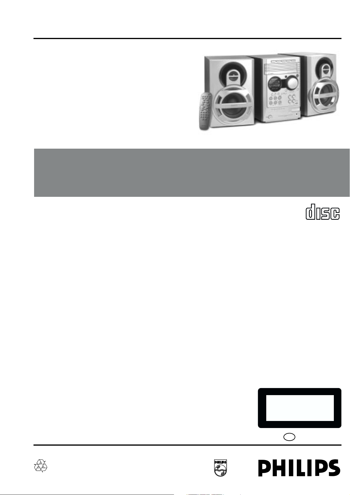
Micro System
Service
Service
Service
MC-500/22/25/30/37
TABLE OF CONTENTS
Page
Location of pc boards & Version variations................1-2
Technical Specifications .............................................1-3
Measurement setup ....................................................1-4
Service Aids, Safety Instruction, etc...........................1-5
Disassembly Instructions & Service positions .............. 2
Service Test Programs ...............................................3-1
Set Block diagram ......................................................4-1
Set Wiring diagram .....................................................5-1
Front Board .................................................................... 6
ECO6 Tuner Board: System Non-Cenelec ................ 7A
System Cenelec........................ 7B
Mains Board................................................................... 8
Combi & Regulator Boards ............................................ 9
5DTC Module (Basic Version) ..................................... 10
Set Mechanical Exploded view & parts list ................. 11
COMPACT
DIGITAL AUDIO
CLASS 1
©
Copyright 2003 Philips Consumer Electronics B.V. Eindhoven, The Netherlands
All rights reserved. No part of this publication may be reproduced, stored in a retrieval system or
transmitted, in any form or by any means, electronic, mechanical, photocopying, or otherwise
without the prior permission of Philips.
Published by BB 0303 Service Audio Printed in The Netherlands Subject to modification
Version 1.0
LASER PRODUCT
GB
3139 785 30270
Page 2
LOCATION OF PRINTED CIRCUIT BOARDS
5D
C
L
T
O
R
5D
T
N
O
D
C
CDC KEY
BOARD
FRONT
BOARD
R
A
O
B
MAINS BOARD
1-2
D
TC
R
A
O
B
D
C
MAINS SOCKET
BOARD
TUNER BOARD
REGULATOR
BOARD
COMBI BOARD
USB PC
LINK
BOARD
VERSION VARIATIONS:
Type /Versions: MC-500
Features &
/22 /25 /30 /37
Board in used:
Aux in /CDR in xxxx
Line Out
Surround Out
Subwoofer Out
Digital Out
Digital in
Matrix Surround
CD Text
Dolby B
RDS x x
News x x
Dolby Pro Logic (DPL)
Incredible Surround
Karaoke Features
Voltage Selector
ECO Power Standby (Clock Display Off) x x
ECO6 Tuner Board - Systems Non-Cenelec x x
ECO6 Tuner Board - Systems Cenelec x x
USB PC LINK xxxx
Page 3

SPECIFICATIONS
1-3
GENERAL:
Mains voltage : 110-127V/220-240V Switchable for /21/21M
120V for /37
230V for /22/25/30/33
Mains frequency : 50/60Hz
Power consumption : < 0.5W at ECO Power Standby
: <15W at Standby (DEMO mode off)
: 80W at Active
Clock accuracy : < 4 seconds per day
Dimension centre unit : 175 x 268 x 316mm
TUNER:
FM
Tuning range : 87.5-108MHz
Grid : 50kHz
100kHz for /37
IF frequency : 10.7MHz ± 25kHz
Aerial input : 75Ω coaxial
300Ω click fit for /37
Sensitivity at 26dB S/N : < 7µV
Selectivity at 600kHz bandwidth : > 25dB
Image rejection : > 25dB
Distortion at RF=1mV, dev. 75kHz : < 3%
-3dB Limiting point : < 8µV
Crosstalk at RF=1mV, dev. 40kHz : > 18dB
MW
Tuning range : 531-1602kHz
530-1700kHz for /21/21M/37
Grid : 9kHz
10kHz for /21/21M/37
IF frequency : 450kHz ± 1kHz
Aerial input : Frame aerial
Sensitivity at 26dB S/N : < 4.4mV/M
Selectivity at 18kHz bandwidth : > 18dB
IF rejection : > 45dB
Image rejection : > 28dB
Distortion at RF=50mV, m=80% : < 5%
Input sensitivity
Aux in (at 1kHz) : 500mV ± 3dB at 600Ω
CDR in (at 1kHz) : 1V ± 3dB at 600Ω
USB (at 1kHz) : 830mV ± 3dB at 600Ω
Output sensitivity
Headphone output at 32Ω : 15mW ± 2dB (Vol. Max.)
5DTC:
Measurement done directly at the connector on the board.
Output resistance : < 100Ω
Output voltage (0dB, 1kHz) : 0.5Vrms ± 1dB (unloaded)
Channel unbalance : < ±1dB
Channel Separation (1kHz) : >60dB
Signal to Noise Ratio (A-weighted) : > 76dBA
Frequency response ( ± 3dB) : 20Hz-20kHz
USB:
Measurement done directly at the connector on the board.
Output resistance : < 1.5kΩ
Output voltage (0dB, 1kHz) : 830mVrms ± 1.5dB
(RL = 33kΩ)
Channel unbalance : < ±1dB
THD + Noise (0dB, 1kHz) : < 0.3%
Channel Crosstalk (0dB, 1kHz) : >40dB
Signal to Noise Ratio (0dB, 1kHz) : > 75dBA (A-weighted)
Frequency response ( ± 3dB) : 20Hz-20kHz
AMPLIFIER:
Output power (6Ω, 1kHz, 10% THD)
L & R : 2 x 50W RMS
Output power (6Ω, 60Hz-12.5kHz, 10% THD)
L & R : 2 x 45W FTC /37
Frequency response within -3dB : 50Hz-16kHz
MAX Sound : ON/OFF
Digital Sound Control (DSC) : Pop/Jazz/Optimal/Rock
Virtual Environment Control (VEC) : Cyber Hall/Concert/
Cinema/Off
Page 4
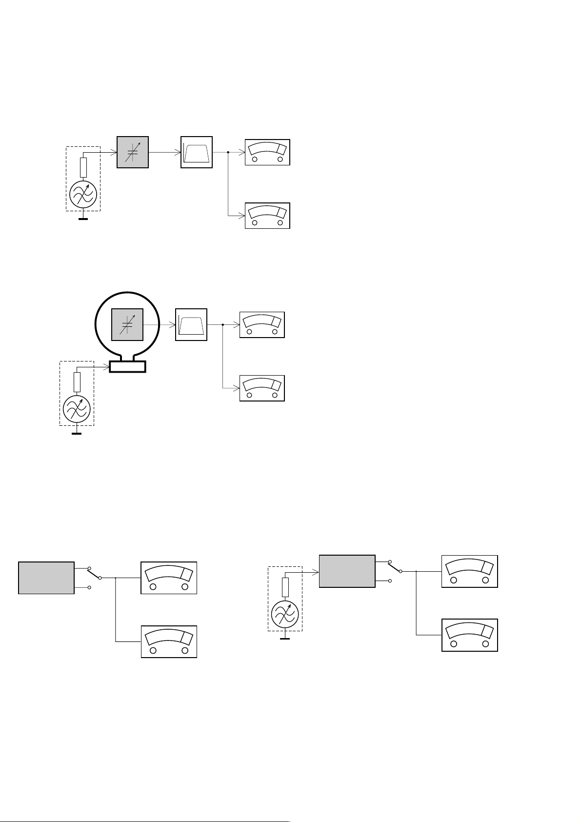
MEASUREMENT SETUP
Tuner FM
1-4
Bandpass
LF Voltmeter
e.g. PM2534
RF Generator
e.g. PM5326
DUT
250Hz-15kHz
e.g. 7122 707 48001
Ri=50Ω
S/N and distortion meter
e.g. Sound Technology ST1700B
Use a bandpass filter to eliminate hum (50Hz, 100Hz) and disturbance from the pilottone (19kHz, 38kHz).
Tuner AM (MW,LW)
RF Generator
e.g. PM5326
Ri=50Ω
DUT
Frame aerial
e.g. 7122 707 89001
Bandpass
250Hz-15kHz
e.g. 7122 707 48001
LF Voltmeter
e.g. PM2534
S/N and distortion meter
e.g. Sound Technology ST1700B
To avoid atmospheric interference all AM-measurements have to be carried out in a Faraday´s cage.
Use a bandpass filter (or at least a high pass filter with 250Hz) to eliminate hum (50Hz, 100Hz).
CD
Use Audio Signal Disc
(replaces test disc 3)
DUT
L
R
SBC429 4822 397 30184
S/N and distortion meter
e.g. Sound Technology ST1700B
LEVEL METER
e.g. Sennheiser UPM550
with FF-filter
Recorder
Use Universal Test Cassette CrO2 SBC419 4822 397 30069
or Universal Test Cassette Fe SBC420 4822 397 30071
LF Generator
e.g. PM5110
DUT
L
R
S/N and distortion meter
e.g. Sound Technology ST1700B
LEVEL METER
e.g. Sennheiser UPM550
with FF-filter
Page 5
SERVICE AIDS
1-5
Service Tools:
Universal Torx driver holder .................................. 4822 395 91019
Torx bit T10 150mm ............................................. 4822 395 50456
Torx driver set T6 - T20 ......................................... 4822 395 50145
Torx driver T10 extended ...................................... 4822 395 50423
Cassette:
SBC419 Test cassette CrO2 ................................. 4822 397 30069
SBC420 Test cassette Fe ..................................... 4822 397 30071
MTT150 Dolby level 200nWb/M ............................ 4822 397 30271
Compact Disc:
SBC426/426A Test disc 5 + 5A ............................ 4822 397 30096
SBC442 Audio Burn-in Test disc 1kHz ................. 4822 397 30155
SBC429 Audio Signals disc .................................. 4822 397 30184
Dolby Pro-logic Test Disc ...................................... 4822 395 10216
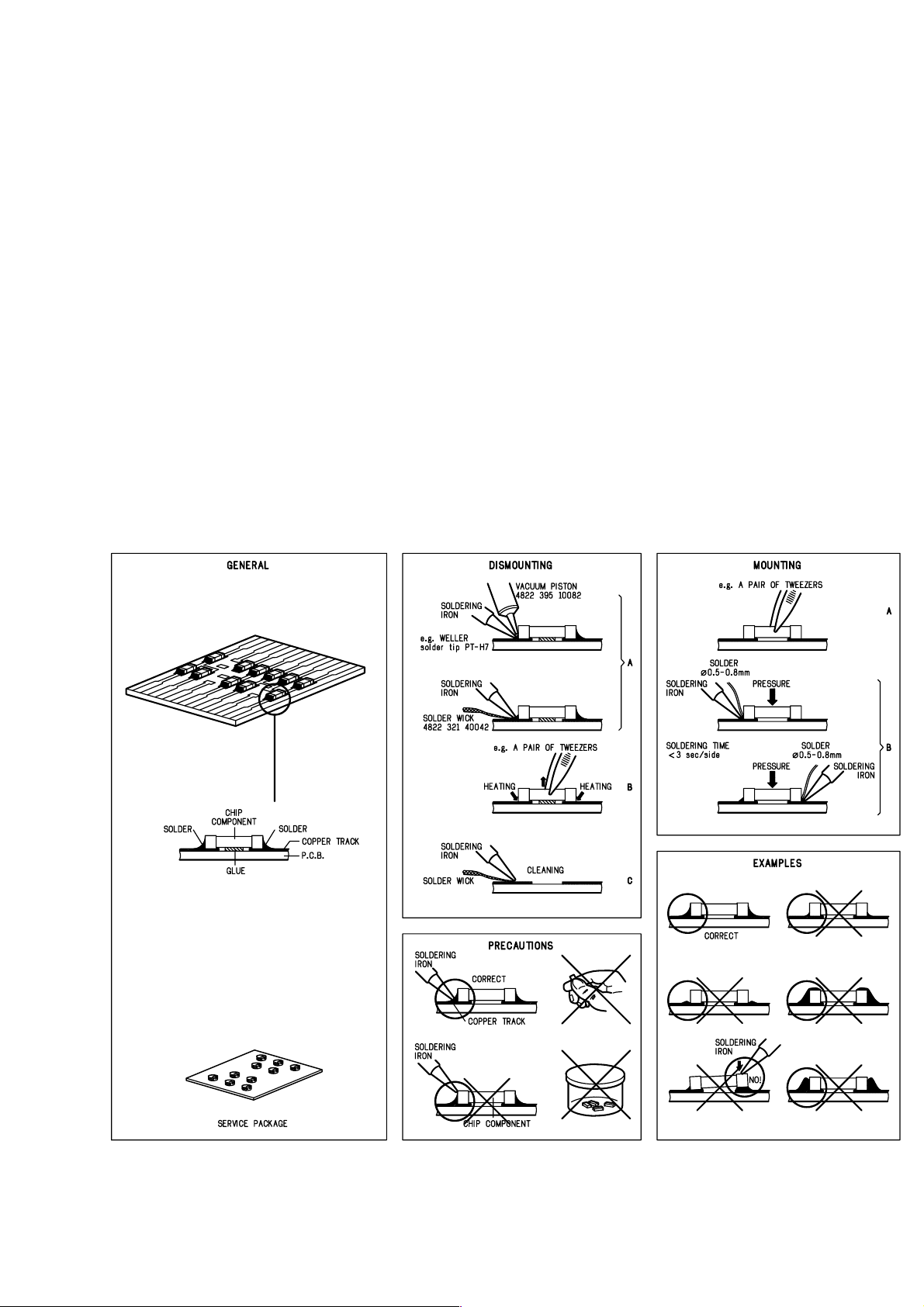
HANDLING CHIP COMPONENTS
ESD Equipment:
Anti-static table mat - large 1200x650x1.25mm ... 4822 466 10953
Anti-static table mat - small 600x650x1.25mm ..... 4822 466 10958
Anti-static wristband .............................................. 4822 395 10223
Connector box (1MΩ) ............................................ 4822 320 11307
Extension cable
(to connect wristband to conn. box) .................. 4822 320 11305
Connecting cable
(to connect table mat to conn. box) .................. 4822 320 11306
Earth cable (to connect product to mat or box) .... 4822 320 11308
Complete kit ESD3
(combining all above products) ......................... 4822 320 10671
Wristband tester .................................................... 4822 344 13999
Page 6
WARNING
GB
All ICs and many other semi-conductors are
susceptible to electrostatic discharges (ESD).
Careless handling during repair can reduce life
drastically.
When repairing, make sure that you are
connected with the same potential as the mass
of the set via a wrist wrap with resistance.
Keep components and tools also at this
potential.
F
ATTENTION
Tous les IC et beaucoup d’autres
semi-conducteurs sont sensibles aux
décharges statiques (ESD).
Leur longévité pourrait être considérablement
écourtée par le fait qu’aucune précaution n’est
prise à leur manipulation.
Lors de réparations, s’assurer de bien être relié
au même potentiel que la masse de l’appareil et
enfiler le bracelet serti d’une résistance de
sécurité.
Veiller à ce que les composants ainsi que les
outils que l’on utilise soient également à ce
potentiel.
1-6
ESD
D
WARNUNG
Alle ICs und viele andere Halbleiter sind
empfindlich gegenüber elektrostatischen
Entladungen (ESD).
Unsorgfältige Behandlung im Reparaturfall kan
die Lebensdauer drastisch reduzieren.
Veranlassen Sie, dass Sie im Reparaturfall über
ein Pulsarmband mit Widerstand verbunden
sind mit dem gleichen Potential wie die Masse
des Gerätes.
Bauteile und Hilfsmittel auch auf dieses gleiche
Potential halten.
WAARSCHUWING
NL
Alle IC’s en vele andere halfgeleiders zijn
gevoelig voor electrostatische ontladingen
(ESD).
Onzorgvuldig behandelen tijdens reparatie kan
de levensduur drastisch doen verminderen.
Zorg ervoor dat u tijdens reparatie via een
polsband met weerstand verbonden bent met
hetzelfde potentiaal als de massa van het
apparaat.
Houd componenten en hulpmiddelen ook op
ditzelfde potentiaal.
I
AVVERTIMENTO
Tutti IC e parecchi semi-conduttori sono
sensibili alle scariche statiche (ESD).
La loro longevità potrebbe essere fortemente
ridatta in caso di non osservazione della più
grande cauzione alla loro manipolazione.
Durante le riparazioni occorre quindi essere
collegato allo stesso potenziale che quello della
massa dell’apparecchio tramite un braccialetto
a resistenza.
Assicurarsi che i componenti e anche gli utensili
con quali si lavora siano anche a questo
potenziale.
GB
Safety regulations require that the set be restored to its original
condition and that parts which are identical with those specified,
be used.
NL
Veiligheidsbepalingen vereisen, dat het apparaat bij reparatie in
zijn oorspronkelijke toestand wordt teruggebracht en dat onderdelen,
identiek aan de gespecificeerde, worden toegepast.
F
Les normes de sécurité exigent que l’appareil soit remis à l’état
d’origine et que soient utiliséés les piéces de rechange identiques
à celles spécifiées.
D
Bei jeder Reparatur sind die geltenden Sicherheitsvorschriften zu
beachten. Der Original zustand des Geräts darf nicht verändert werden;
für Reparaturen sind Original-Ersatzteile zu verwenden.
“Pour votre sécurité, ces documents
doivent être utilisés par des spécialistes agréés, seuls habilités à réparer
votre appareil en panne”.
CLASS 1
LASER PRODUCT
GB
Invisible laser radiation when open.
Avoid direct exposure to beam.
Osynlig laserstrålning när apparaten är öppnad och spärren
är urkopplad. Betrakta ej strålen.
Warning !
S
Varning !
3122 110 03420
I
Le norme di sicurezza esigono che l’apparecchio venga rimesso
nelle condizioni originali e che siano utilizzati i pezzi di ricambio
identici a quelli specificati.
"After servicing and before returning set to customer perform a
leakage current measurement test from all exposed metal parts to
earth ground to assure no shock hazard exist. The leakage current
must not exceed 0.5mA."
Varoitus !
SF
Avatussa laitteessa ja suojalukituksen ohitettaessa olet alttiina
näkymättömälle laserisäteilylle. Älä katso säteeseen!
DK Advarse !
Usynlig laserstråling ved åbning når sikkerhedsafbrydere er
ude af funktion. Undgå udsaettelse for stråling.
Page 7
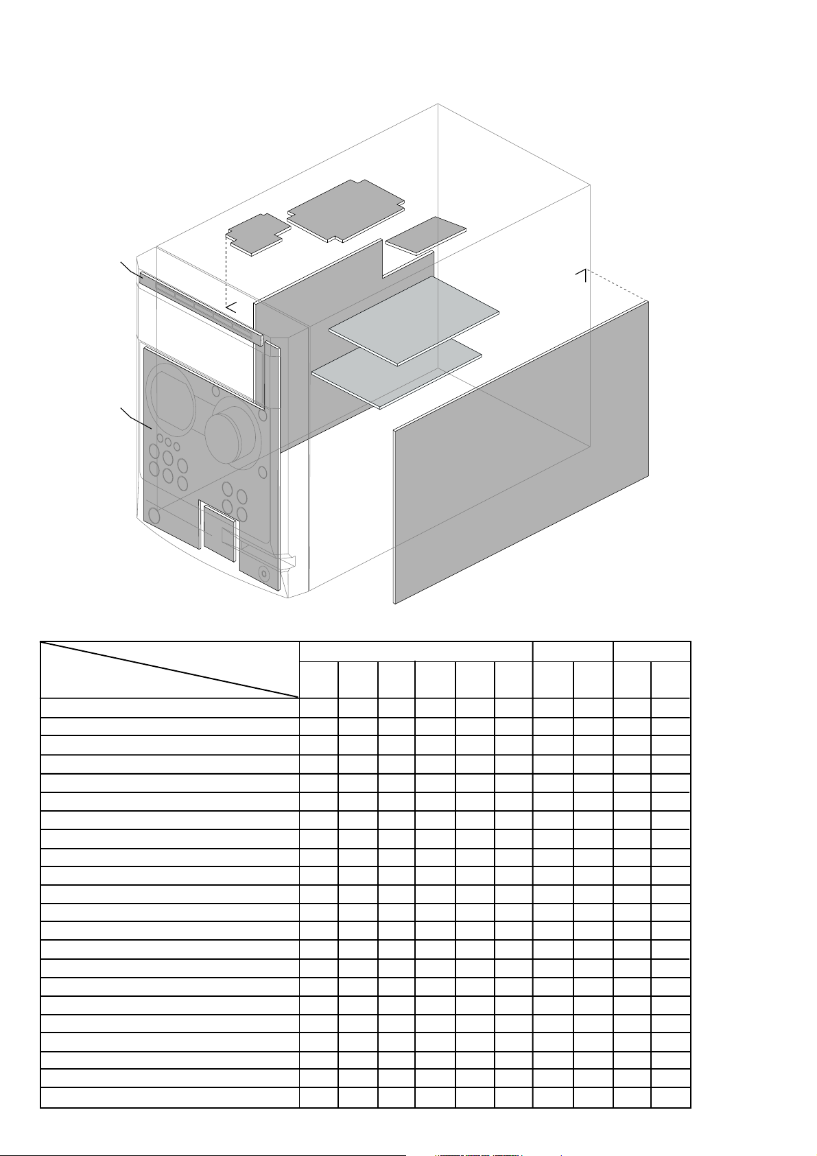
DISMANTLING INSTRUCTIONS
Dismantling of the 5DTC Module
2-1 2-1
1) Loosen 4 screws and remove the Cover Top (pos 255) by
sliding it out towards the rear before lifting up.
- 2 screws on the rear
- 1 screw each on the left & right side
2) Loosen 3 screws each to remove the Panel Left (pos 253)
and Panel Right (pos 254). The Panels are remove by
sliding it towards the rear and outwards.
- 1 screw on the side
- 2 screws on the rear
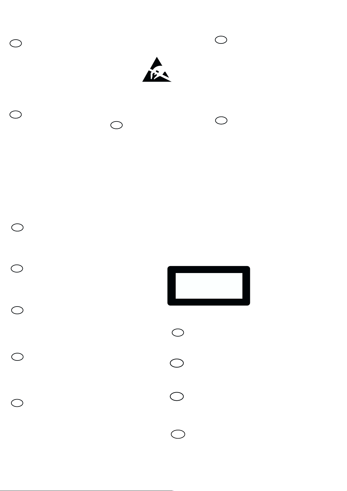
3) Take a paper clip or any stiff wire diameter of 1mm-1.5mm.
Place the set in position and insert the paper clip or stiff
wire as shown in Figure 1.
Figure 1
4) To remove the Cover CD Orn (pos 111), you have to feel
and give a push in the correct direction (see Figure 1) and
correct position (see Figure 2) to release the catch of the
Cover CD Orn before removing it out.
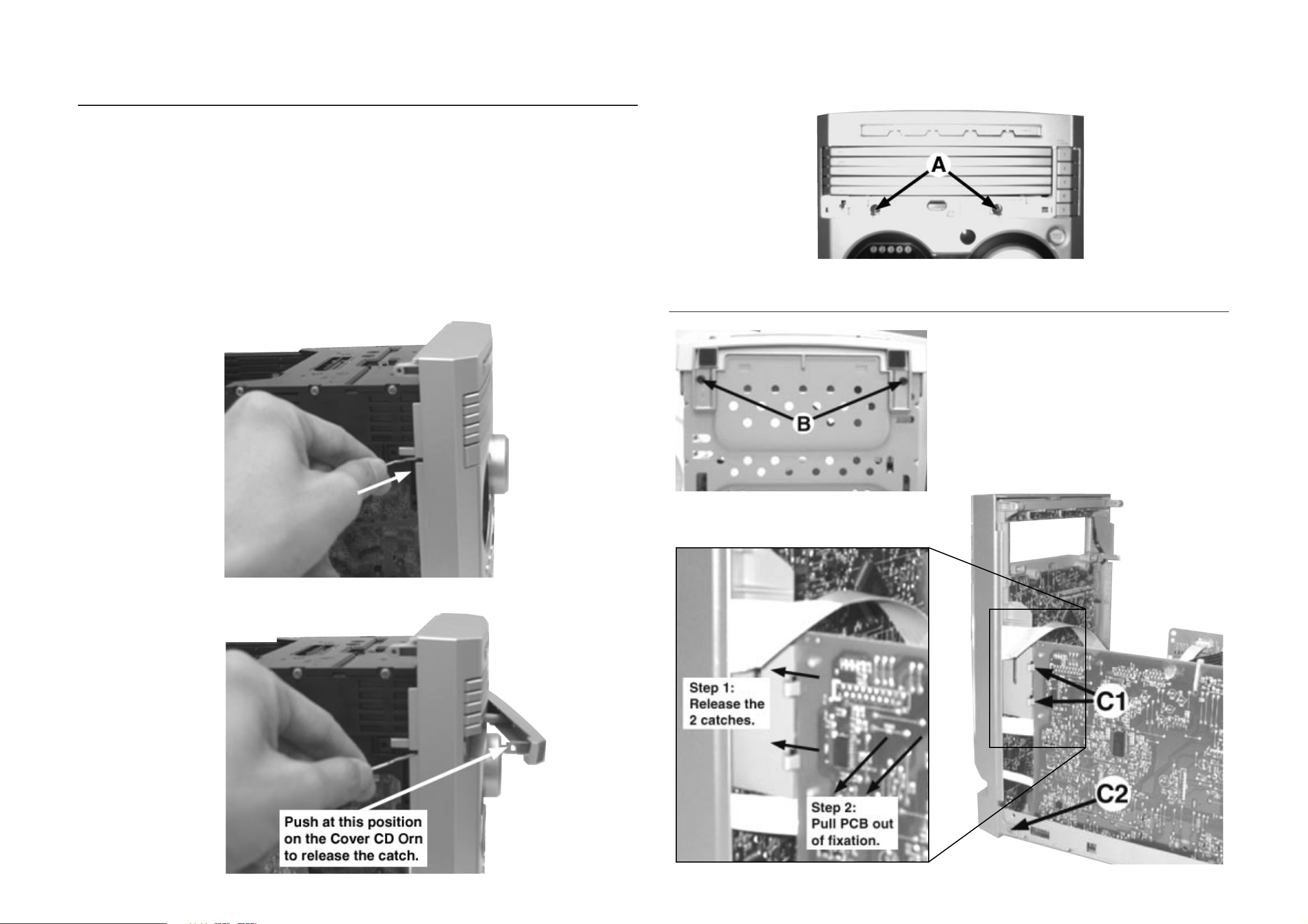
5) Loosen 4 screws A (see Figure 3 and Figure 9) to remove
the 5DTC Module (pos 1103).
- 2 screws on the front
- 2 screws on the rear
Note : For information on the 'Emergency opening of the
trays' of the 5DTC Module, refer to Chapter 10
(Page 10-7).
Figure 3
Detaching the Front Panel assembly from the Bottom/Rear assembly
1) Remove 2 screws B (pos 282) as shown in Figure 4 from
the bottom of the Cabinet Front (pos 101).
2) Release the fixation of the Combi Board (pos 1102-1003)
to Bracket Combi (pos 252) by releasing the 2 catches C1
(see Figure 5) and pulling the Combi Board outwards as
shown in Figure 6.
3) Uncatch 2 catches C2 (see Figure 5) on the left & right
sides of the Cabinet Front (pos 101) and slides the Front
Panel assembly out towards the front.
Figure 2
Figure 4
Figure 6
Figure 5
Page 8
DISMANTLING INSTRUCTIONS
2-2
2-2
Dismantling of the Front Panel assembly
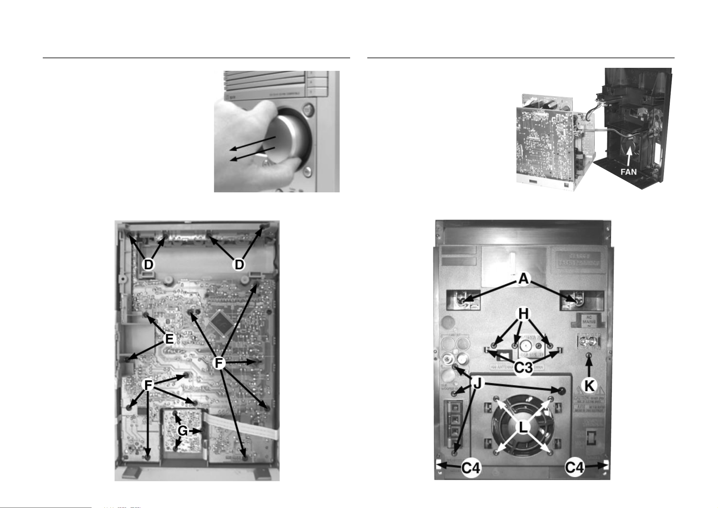
1) The Knob Volume (pos 136) can be remove by pulling it out
in the direction as shown in Figure 7.
2) Loosen 4 screws D (see Figure 8) to remove the Bracket
Top (pos 251) and CDC Key Board (pos 1105B).
3) Loosen 2 screws E (see Figure 8) to remove the Bracket
Combi (pos 252).
4) Loosen 9 screws F (see Figure 8) to remove the Front
Board (pos 1105A).
5) Loosen 3 screws G (see Figure 8) to remove the USB PC
LINK Board (pos 1106).
Figure 8
Figure 7
Dismantling of the Rear Panel assembly
1) Loosen 3 screws H and 2 catches C3 (see Figure 9)
to remove the Tuner Board assembly.
2) Loosen 1 screw K (see Figure 9) to free the Mains
Socket Board (pos 1102-1001B).
3) Loosen 4 screws J and 2 catches C4 (see Figure 9)
to remove the Cabinet Rear (pos 256) by sliding it
out towards the rear (see Figuer 10).
Note : Tuner Board assembly and Mains Socket
Board can also be remove together with the
Cabinet Rear.
4) Loosen 4 screws L (see Figure 9) to remove the Fan
(pos 1104) from the Cabinet Rear.
Figure 10
Figure 9
Page 9
DISMANTLING INSTRUCTIONS
2-3 2-3
Repair Hints & Service Positions
1) During repair it is possible to disconnect the ECO6 Tuner
board and/or 5DTC Module completely unless the fault is
suspected to be in that area. This will not affect the
performance of the rest of the set.
Service position A
Service position B
Note: The flex cables are very fragile, care should be taken
not to damage them during repair. After repair, be
very sure that the flex cables are inserted properly
into the flex sockets before encasing, otherwise faults
may occurs.
Service position C
Page 10
3-1 3-1
SERVICE TEST PROGRAM
TUNER
TEST
TUNER
Button pressed?
Y
Display Tuner Version
"ccc"
TUNER
Button pressed?
Service frequencies are
copied to the RAM (see Table 1)
Tuner works normally except:
PROGRAM button
Disconnect
Mains cord ?
Y
Service Mode left
PRESET
10
11
Europe
"EUR"
1
87.5MHz
2
108MHz
3
531kHz
4
1602kHz
5
558kHz
6
1494kHz
7
87.5MHz
8
87.5MHz
9
87.5MHz
87.5MHz
98MHz
Note: * Depending on the selected grid frequency (9 or 10kHz).
By holding the PROG and R buttons depressed while switching on the Mains supply, one
of the undermentioned features will be activated:
- the tuning grid frequency is toggled between 9kHz and 10kHz for the Oversea (/21) version.
- the extended FM1 (65.81MHz - 74MHz) is toggled on and off for East Eur. (/34) version.
N
N
N
East Europe
"EAS"
87.5MHz
108MHz
531kHz
1602kHz
558kHz
1494kHz
87.5MHz
87.5MHz
87.5MHz
87.5MHz
98MHz
QUARTZ
TEST
O
Button pressed?
Y
Display shows
32K
Output at (Front Board)
pin 19 of uP = 2048Hz
O
Button pressed?
Y
Display shows
12M
Output at (Front Board)
pin 19 of uP = 2,929.6875Hz
9
Button pressed?
Y
East Eur. Extended-band
"EAS"
65.81MHz
108MHz
74MHz
87.5MHz
531kHz
1602kHz
558kHz
1494kHz
98MHz
70.01MHz
65.81MHz
Table 1
N
N
N
USA
"USA"
87.5MHz
108MHz
530kHz
1700kHz
560kHz
1500kHz
98MHz
87.5MHz
87.5MHz
87.5MHz
87.5MHz
** Choose
level
by pressing
R
R
Oversea
"OSE"
87.5MHz
108MHz
531/530kHz*
1602/1700kHz*
558/560kHz*
1494/1500kHz*
87.5/98MHz*
87.5MHz
87.5MHz
87.5MHz
98/87.5MHz*
To start service test program
™
hold
depressed while
plugging in the mains cord
Display shows the
ROM version
"S-Vyy"
(Main menu)
CD
Button pressed?
Y
Note : Disc should be available on the tray before entering the Service Test Mode.
STEP
DISPLAY
5DTC-Vnn
1
MP3CD’02
2
TI-Vnn
**3
TI BUS
**4
TI SLD I
**5
TI SLD O
**6
TI FOC
**7
& PROG
5DTC CONTROL &
MP3 CD MODULE
TEST
N
(For MC-M570 only)
MESSAGE
OKAY
-
-
-
BUS OK
-
-
FOC OK
Error code
E1000
E1001
E1002
E1003
E1005
E1006
E1007
E1008
E1020
E1061
E1079
S refers to Service Mode
V refers to Version
yy refers to Software version number of the uProcessor
(counting up from 01 to 99)
SERVICE PLAY MODE
(For MC-500 only)
ECO
Button pressed?
ERROR
5DTC-ER
BUS ER
FOC ER
ACTION
Version of the 5DTC control software (nn = Version Number).
-
Indicates the module used.
-
Version of the MPEG software (nn = Version Number).
Communication test between the Main uP and CD Module
-
CD SLEDGE MOTOR is moved in.
-
CD SLEDGE MOTOR is moved out.
FOCUS SERVO Test.
Press 9 to exit
Error Description
Focus Error
Triggered when the focus cannot be found within a certain time when starting up the CD, or if the focus
is lost for more than a certain time during playing of CD.
Radial Error
Triggered when the radial servo is off-track for a certain time during playing of CD.
Sledge In Error
The sledge did not reach its inner position (inner-switch is still close) before approximately 6 seconds
have passed by. Inner-switch or sledge motor problem.
Sledge Out Error
The sledge did not come out of its inner position (inner-switch is still open) before approximately 250ms
have passed by. Inner-switch or sledge motor problem.
Jump Error
Triggered in normal play when the jump destination could not be found within a certain time.
Subcode Error
Triggered when a new subcode was missing for a certain time during playing of CD.
PLL Error
The Phase Lock Loop could not lock within a certain time.
Turntable Motor Error
Generated when the CD could not reached 75% of speed during start-up within a certain time. Disc
motor problem.
Focus Search Error
The focus point has not been found within a certain time.
The tray could not enter the inside position and is opening again. This can happen if the tray is blocked
such that it cannot go fully inside, or if the 5DTC control module is defective and never closes.
The tray could not reach the outside position and is stopped at its blocked position. This can happen if
the tray is blocked such that it cannot go fully outside, or if the 5DTC control module is defective and
never opens.
Table 2
Set is in Service PLAY Mode
CD
Button pressed?
Display shows "5DTC-Vnn" -
Version of 5DTC control software
(nn = Version Number).
DTC works as in normal operation.
In case of failures, error
codes according to Table 2
will be displayed.
The Service Play Mode is intended
to detect and identify the failures
in the CD Mode.
In this mode the DTC works as in
normal operation. The electronics
will still function even when an error
is detected so that repair activities
can be carried out.
Figure 1 Figure 2
ADC
TEST
N
Y
N
Y
ADC Test is used for checking the
ADC inputs to the microprocessor.
The display shows an ADC value
between 0 and 255 for an input
signal between 0 and 5V.
PLAY
Button pressed?
Y
Display shows "ADC1 Value"
for ADC 1
(Input Line - SA)
PLAY
Button pressed?
Y
Display shows "ADC2 Value"
for ADC 2
(Input Line - Option)
PLAY
Button pressed?
Y
Display shows "ADC3 Value"
for ADC 3
(Input Line - AmNtc)
9
Button pressed?
Y
TEST
EEPROM TEST A test pattern will be sent to the EEPROM.
TEST
DEMO TOGGLE
ROTARY
ENCODER TEST
MICRONAS
FIRMWARE
VERSION
LEAVE SERVICE
TEST PROGRAM
N
N
N
N
Activated with
R
9 to Exit
QEEPROM FORMAT
MAX SOUND
Rotary Volume
Knob
USB PC LINK
9 to Exit
Disconnect
mains cord
DISPLAY
TEST
VEC
Button pressed?
Y
Display shows Figure 1
and switch all LEDs on
(except ECO POWER LED)
VEC
Button pressed?
Y
Display shows Figure 2
and switch alternate LEDs on
(see Table 3)
9
Button pressed?
Y
LEDs
TUNER
AUX
USB PC LINK
MAX SOUND
USB Indicator
MC-M570
CD
OFF
ON
OFF
ON
OFF
ON
Table 3
N
N
N
MC-500
-
-
-
-
OFF
ON
Various
other Tests
ACTION
"PASS" is displayed if the uProcessor read back the test pattern
correctly, otherwise "FAIL" will be displayed.
Load default data. Display shows "NEW" for 1 second.
Caution! All presets from the customer will be lost!!
Pressing this button will toggle between DEMO ON and DEMO
OFF. The DEMO status will scroll once across the Display.
Display shows value for 2 seconds.
Values increases or decreases until Volume Maximum (0dB) or
Volume Minimum (VOL MUTE) is reached.
To read out the Firmware Version of IC UAC3553 on the USB
PC LINK Board.
Display shows "Vxxxx" (xxxx = Firmware Version number).
Micro 2003_MC-500 & MC-M570_Service Test Program (dd wk0242)
Page 11
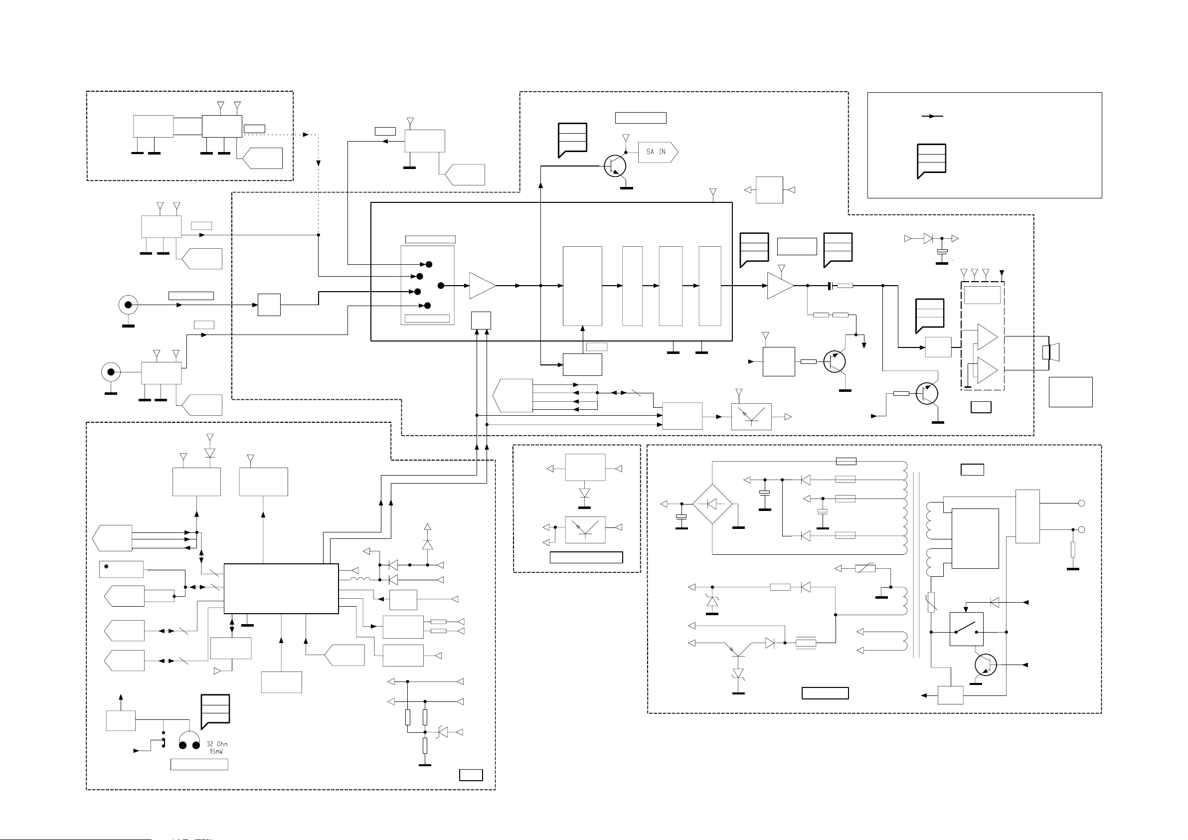
SET BLOCK DIAGRAM
-6dB Track
MP3
D
A
FOR MP3 VERSION
+12V_M
+CD
-6dB Track
5DTC
DM
CONTROL
AUX / CDR
A
USB
D
D
500mV / 1000mV
+12V_A
+C
USB
A
CONTROL
250mV
CDC
830mV
USB
M
+5V6
+CD
5DTC
+12V_M
D
250mV
CONTROL
CDC
ATTN.
-8.5dB
4-1 4-1
125mV
+12V_A
ECO6
A
SOFTWARE CONTROL
SOURCE SELECTOR
FM (67.5 kHz)
AM (80% MOD)
TUNER
CONTROL
I2C
I2C DATA
I2C CLK
CONTROL
COMBI
HP_DET
MUTE_HP
AMP_ON
AMP_MUTE
500mV
76dBA
16dB
INCREDIBLE
SURROUND
INTERFACE
SIMPLE
IS FILTER
500mV
SA BUFFER
+12V_A
A
VOL. 1
I2C DATA
I2C CLK
TREBLE
&
BASS
A
M62320FP
I2C SHIFT
REGISTER
TDA7468
VOL. 2
D
+9.1V
CD_ON
+9.1V
LEFT/RIGHT
HP_MUTE
+5V6
500mV
85dBA
16dB
+9V
REG
+12V_A
NJM4556AM
+5V6
MUTE
+12V_A
HEADPHONE
AMPLIFIER
+5V_CD
2.50V
85dBA
3dB
39R 39R
HP_OUT
A
AMP_MUTE
NOTE :
B
MAIN SIGNAL PATH
MEASUREMENTS ARE IN AUX MODE :
XX mV
YY dBA
ZZ dB
FOR CLASS G SWITCH
1.90V
67dBA
3.0dB
LEFT/RIGHT
LEVELS AT MAX VOL
S/N AT 500mW
HEADROOM (1% THD) WRT TO LEVEL AT MAX VOL
+50V
B1
A1
POWER
AMPLIFIER
AN7591
+
-
+
-
COMBI
AMP_ON
C1
ATTEN.
Rin = 3k
A
L/R SPEAKER
2 X 40W
2 X 6 OHMS
POWER
CONTROL
RDS
DECODER
TUNER
CONTROL
5DTC
CONTROL
CONTROL
HP_DET
HP DET
USB
NTC
PWDN
LPC
+C
ECO POWER
LED
+D
650mV
78dBA
3.2dB
EEPROM
+5V6
USB/MAX LEDS
uP
TMP88CU74YF
D
ADC
KEY SCAN
SA IN
I2C DATA
+C
-33V
F1x
F2x
I2C CLK
IR EYE
FTD
VOLUME
CONTROL
NTC
FUSE
FUSE
FUSE
FUSE
TRAFO
L
FOR -/21 ONLY
VOLTAGE
SELECTOR
F1
F2
+5V6_ECO
LPS
SMPS
MAINS
CHOKE
(NOT USED FOR -/37)
(ONLY FOR -/37)
A2
STBY TRANSFORMER
(NOT USED IN -/21 & -/37)
LOW_POWER_CONTROL
N
10M
+5V6
+D
+5V6
+5V6_ECO
+C
F1x
F2x
+D
F1
F2
-33V
+12V_A
+12V_D
REGULATOR
7805
REGULATOR / STABILISER
A2
B1
A1
A1
PWDN
B
-33V
A2
POWER SUPPLY
HP_OUT
HEADPHONE
FRONT
Block Diagram_3139 119 35490 dd wk0251
Page 12
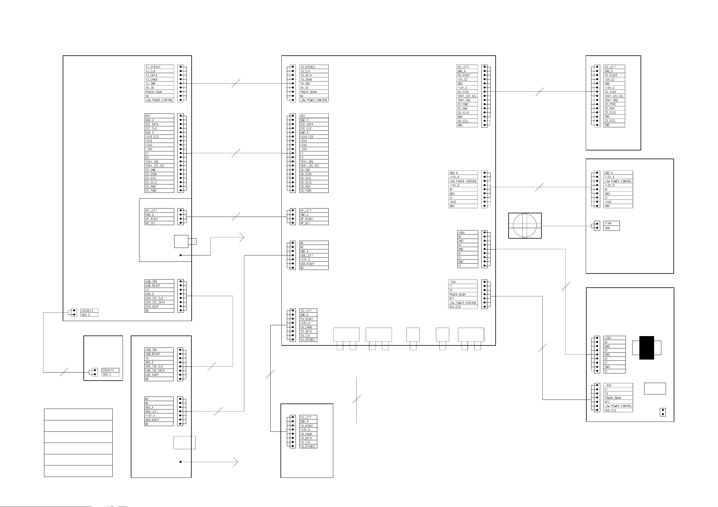
SET WIRING DIAGRAM
5-1
5-1
FRONT
(1105)
FCS 1402
FCS 1401
FCS 1301
## 8101
1
1
1
1302
1
FCS 1824
8009
9P/180mm/AD
FCT 1025
1
FCT 1026
1
FCT 1018
8003
15P/480mm/BD/Fold
5DTC
8008
19P/180mm/AD/Fold
COMBI
(1103)
(1102)
EHT 1314
8200
9P/120mm
FCT 1014
8007
4P/120mm/AD
HP
## 8101
1P/180 mm
TO BOTTOM PLATE
1
EHT 1302
FCT 1022
1
1
FAN
(1104)
2P/260mm
EHT 1402
1
EHT 1400
1
REGULATOR/
STABILISER
(1102)
BI 8100
CDC KEY
(1105)
8100
2P/100mm
EHT 1336
LEGEND
EHS - EH SIDE ENTRY
EHT - EH TOP ENTRY
FCS - FFC SIDE ENTRY
FCT - FFC TOP ENTRY
BI - BOARD IN ENTRY
FCT 1400
FCS 1703
FCS 1702
USB
(1106)
1701
FCT 1304
1
8002
9P/220mm
SUPPLY (MAINS)
FCT 1013
1
1
1001-A
1
8006
8P/100mm/BD
8004
8P/280mm/AD/Fold
1
8005
7P/180mm/AD
FCT 1120
1
USB
## 8011
1P/100 mm
TO BOTTOM PLATE
ECO6
AUX-IN
## 1001-B
LINE OUT
8010
1P/180 mm
FROM TUNER’S METAL STRIP
TO AUX’S METAL STRIP
ON REARCAB
## 1004
SUBWOOFER OUT
(1101)
## 1006
DIGITAL OUT
1307
LOUDSPEAKER
## - PROVISION
$$ - FOR SETS WITH ECO FEATURE
8001
7P/220mm/AD
Wiring Diagram_3139 119 35500 dd wk0251
(1102)
EHT 1203
1
1
FCT 1209
(5001)
TRAFO
PIN TYPE
$$ LPS
TRAFO
1204
1
N
L
Page 13
(10G)
(2G~9G)
6-1
6-1
FRONT BOARD
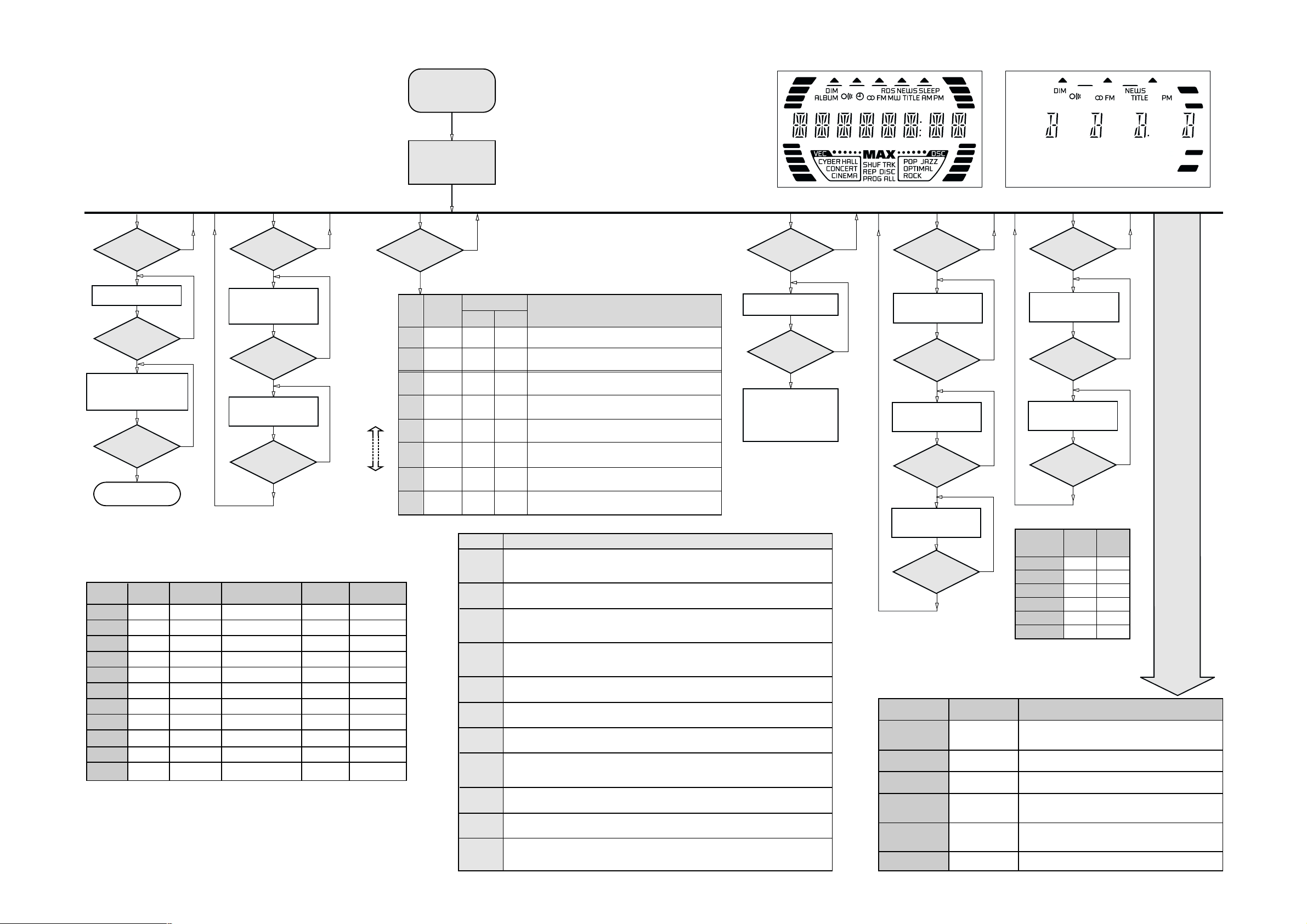
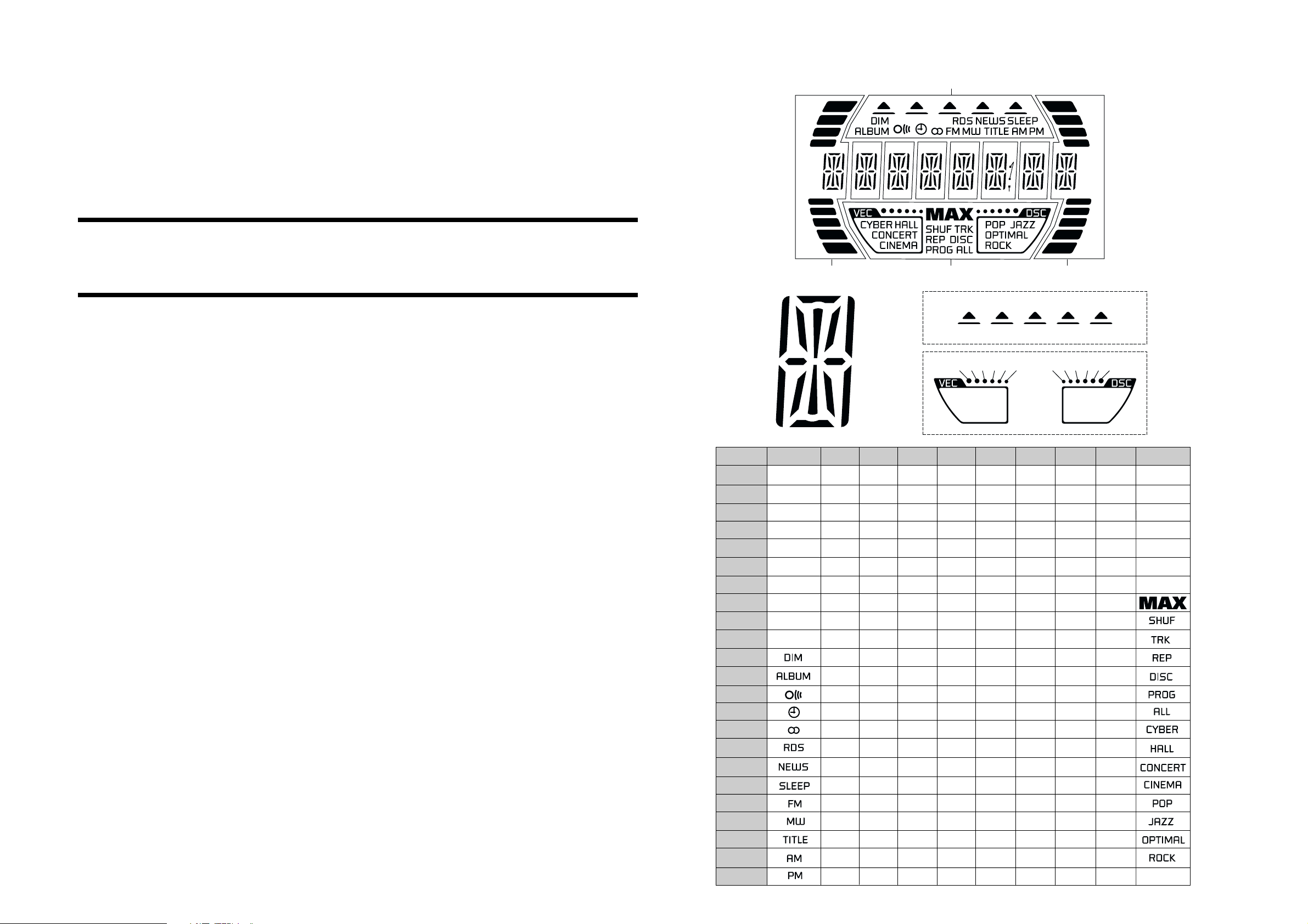
FTD DISPLAY PIN CONNECTION
B1
B2
B3
B4
B5
B6
B7
B8
B9
a
j k bhf
(2G~9G)
g
m
1G
3G 4G 5G 6G 8G7G
10G2G
S6 S5 S4 S3 S2 S1
Dp
B1
B2
B3
B4
col
B5
B6
B7
B8
B9
9G
S5S4S3S2S1
(1G)
S10S9S8S7S6
S1 S2 S3 S4 S5 S6
TABLE OF CONTENTS
FTD Display Pin Connection ........................................... 6-1
Front Board - Component layout .....................................6-2
Front Board - Chip layout ................................................ 6-3
Front Board - Circuit diagram (Part 1)............................. 6-4
Front Board - Circuit diagram (Part 2)............................. 6-5
Front Board - Circuit diagram (Part 3)............................. 6-6
CDC Key Part - Layout & Circuit diagram .......................6-7
Variant Table .................................................................... 6-7
Electrical parts list............................................................ 6-8
P1
P2
P3
P4
P5
P6
P7
P8
P9
P10
P11
P12
P13
P14
P15
P16
P17
P18
P19
P20
P21
P22
P23
e
p n cr
S7 S7
(10G)
d
1G
S1
S2
S3
S4
S5
S6
S7
S8
S9
S10
2G
j , p
m
B1
B2
B3
B4
B5
B6
B7
B8
B9
3G
a
h
k
b
f
g
c
e
r
n
d
-
a
h
j , p
k
b
f
m
g
c
e
r
n
d
-
-
-
-
-
-
-
-
-
-
4G
j , p
m
5G
a
h
k
b
f
g
c
e
r
n
d
-
-
-
-
-
-
-
-
-
-
a
h
j , p
k
b
f
m
g
c
e
r
n
d
-
-
-
-
-
-
-
-
-
-
6G
j , p
m
7G
a
h
k
b
f
g
c
e
r
n
d
-
-
-
-
-
-
-
-
-
-
a
h
j , p
k
b
f
m
g
c
e
r
n
d
col
Dp
-
-
-
-
-
-
-
-
8G
a
h
j , p
k
b
f
m
g
c
e
r
n
d
-
-
-
-
-
-
-
-
-
-
9G
j , p
B1
B2
B3
B4
B5
B6
B7
B8
B9
10G
a
h
k
b
f
m
g
c
e
r
n
d
-
S1
S2
S3
S4
S5
S6
S7
-
Page 14
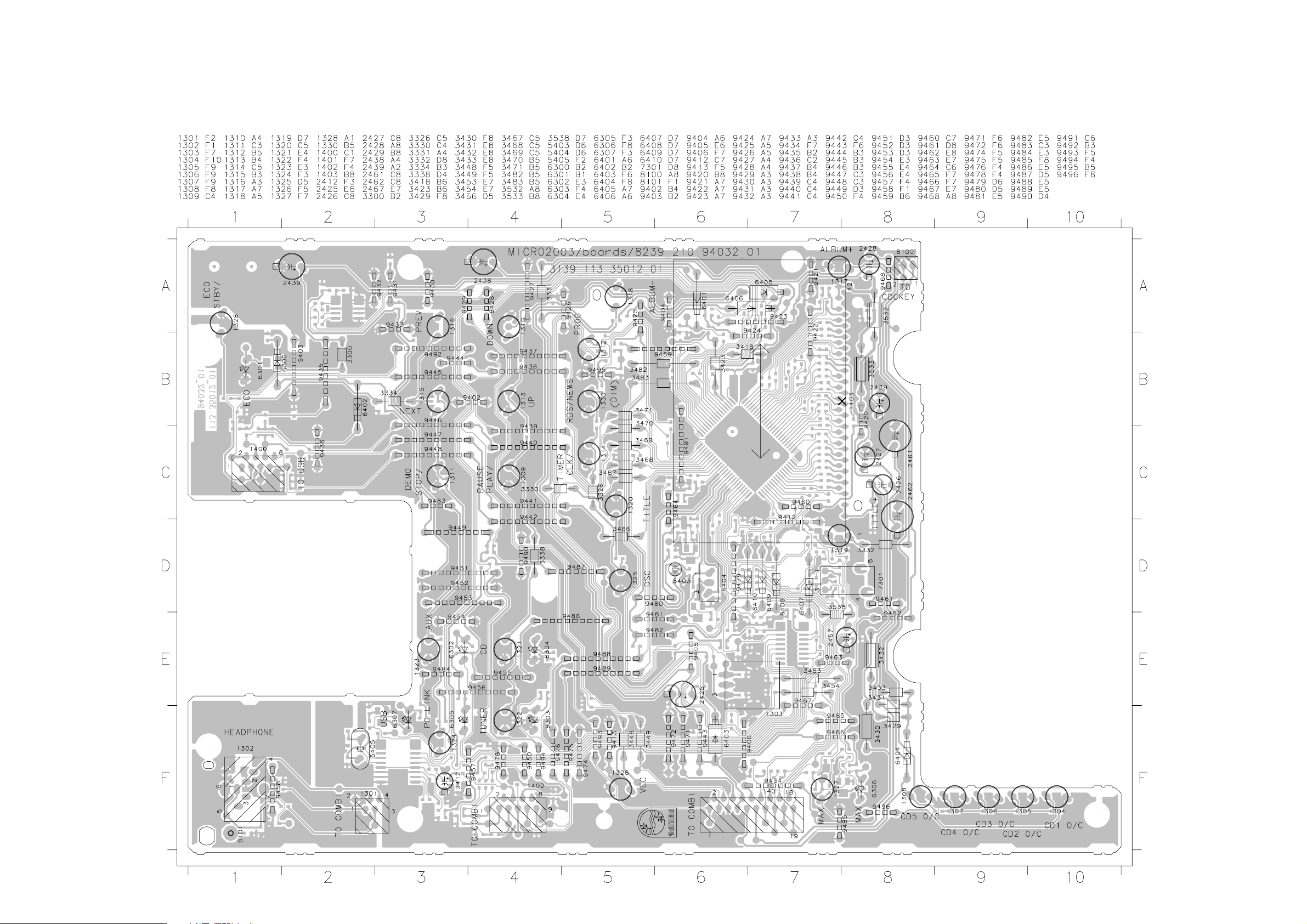
FRONT BOARD - COMPONENT LAYOUT
6-2
6-2
This assembly drawing shows a summary of
all possible versions. For components used
in a specific version see schematic diagram
and respective parts list.
3139 113 3501 pt2 dd wk0251
Page 15

FRONT BOARD - CHIP LAYOUT
This assembly drawing shows a summary of
all possible versions. For components used
in a specific version see schematic diagram
and respective parts list.
6-3 6-3
3139 113 3501 pt2 dd wk0251
Page 16
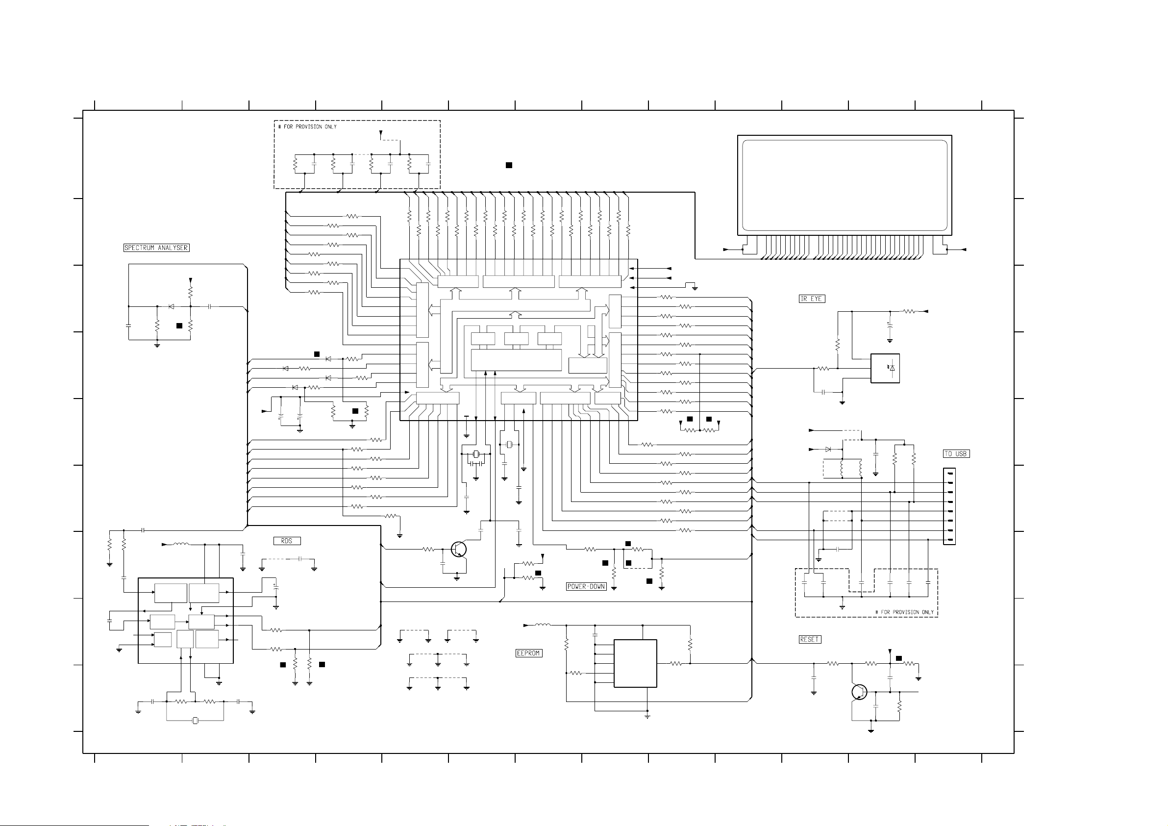
FRONT BOARD - CIRCUIT DIAGRAM (Part 1)
1 2345678910111213
Front Board
Circuit Diagram (Part 1)
A
B
TUENABLE
VDDD
VREF
SYNC
RDCL
RDDA
QUAL
VSSD
D
SA_IN
2409
SA
100n
2415
D
3
10
16
2
1
47p
LedShStr
LedShData
LedShClk
LedEnable
-33V
TRAY_IIC_SCL
CD_PORE__uC_RESET
TRAY_IRQ
TUDATA
TUCLK
TUSTEREO
CD_RAB__uP_FRAME
MpOscShiftTu
D
D
+D
3404
C
1N4148
3405
220n
2407
470K
6401
3406
680K
33K
2406
1u
D
D
E
F
2416
1n
+D
1K5
10K
3407
3408
2411
D
7403
SAA6581T
560p
2410
560p
15
4
8
7
9
MPX
SCOUT
CIN
TCON
MODE
57 Khz
BANDPASS
(8th ORDER)
CLOCKED
COMP
TEST
CTRL
G
H
D
I
2408
47p
D
5406
2u2
VSSA
OSC
&
CLK
OSCI14OSCO
13
3410
220K
5405
AT-51
4.9V
512
VDDA
POW SUPPL
&
RESET
RDS/RBDS
DEM
SIGNAL
QUALITY
DET
VSSA
611
3409
2K2
1 234567891011
9457
2412
3417
1K
3416
1K
1N4148
2461
D
6408
50V2u2
P15
P16
P17
P18
P19
P20
P21
P22
P23
6410
1N4148
22u
50V
3541
3418
2471
2462
47n
10K
G9
3523
1K
50V 22u
FTD
10K
3419
D
6-4 6-4
DC Voltages During Active Play.
2402
3517
3519
3521
3525
1K
1K
1K
1K
10K
ADC
TU
100p
1N4148
1N4148
6407
6409
3542
3514
1K
3516
1K
3518
1K
3520
1K
# 3544
10K
2403
G10
3513
3515
3522
10K
TURdsDATA
9422
100p
1K
1K
1K
3524
1K
D
3527
470R
3458
1K
3460
1K
3462
1K
TURdsClk
3545
3401
10K
3526
470R
3457
470R
3459
1K
3461
470R
-33V
4412
10K
2400
G2
# 3546
10K
MpOscShiftTu
Reset
100p
65
66
67
68
69
70
71
72
73
74
75
76
77
78
79
V24
V25
V26
V27
V28
V29
V30
V31
V32
V33
V34
V35
V36
VKK
-SCK1
SI1
1
D
FTD
3402
P14
3512
V23
SO1
9412
USB
TU
10K
100p
2401
G1
P11
P12
P13
1K
1K
3510
1K
1K
3511
3509
V21
V20
V22
8-Bit h. break. v.
80k pull
down
8-Bit h. breakdown v.
out. port w. latch P9
PD
source open
drain 80k p.d.
5-Bit h. breakd. v.
out w. latch
8-Bit Input/Output
(tri-state)
P03
P04
P05
4
3
3463
4K7
2418
D
9403
D
9430
D
Legend :
P7
P9
P8
P10
1K
1K
3506
3508
V19
P0
P06
33p
# 9402
TU
9404
9406
3504
1K
1K
3507
3505
V16
V17
V18
V15
VFT driver circuit (automatic display)
XIN
VSS
XOUT
P07
8809
7
D
5404
D
22p
# 2479
D
2420
7404
BC847B
D
IIC
ADC
CD
Note :
Values in Bracket are DC Voltages at Standby (Clock Mode).
Values in Square Bracket are DC Voltages at Low Power Standby.
Note : Some values may varies, see respective parts list for correct value.
Refer to Variant Table.
#
For Provision Only .
P6
1K
3503
V14
8-Bit high breakdown voltage 8-Bit high breakdown v.
output port with latch output port with latchout w. latch P8
-RESET
10 11 12 13 14 15 16 17 18 19220 21 22 23 24
22p
P5
54555657585966061626364
P4
3502
1K
V13
CPU
sink o.
8-Bit I/O P2
sink o.drain
XTOUT
5403
32K768
2419
Options
P2
P1
P3
1K
3501
V12
ROMRAM
XTIN
22p
G1
1K
1K
3498
3500
1K
1K
3499
3497
V8
V9
V11
V10
P7 P6
80k pull down80k pull down
P6-P9 source open drain
Program
Counter
drain
8-Bit Input/Output
(tri state)
TEST
-STOP
-INT0
-INT1
D
D
22p
2456
D
2p2
2421
D
+C
3420
2K7
3423
1K8
D
5407
+D
2u2
G5
1K
1K
3496
3494
3492
1K
3495
V6
1K
3493
V4
V3
V5
1K
V7
80k pull down
8-Bit A/D
Converter
3-B. I/O P3
P1
( tristate )
-DV0
6K8
3426
INT2
TC1
TC4
3464
1K
2455
1K
TC2
3425
1K
1K
3491
V2
4-Bit In/Output
8-Bit Input/Output
INT4
3438
7401
M24C02
100n
1
E0
2
E1
3
E2
6
SCL
7
WC_
3490
414243444546474849550515253
V1
VAREF
VASS
AIN13
P5
(tri-state)
P4
(tri-state)
-SCKO
SCL
1M
D
G10
1K
1K
3489
40
V0
VDD
39
38
37
36
AIN12
35
AIN11
34
AIN10
33
AIN7
32
AIN6
AIN5
31
30
AIN4
29
AIN3
28
AIN2
27
AIN1
26
AIN0
25
SCA
TMP88CU74YF
7400
3437
680K
4400
4.9V
VCC
4.9V [4.9V]
4.9V [4.9V]
3474
470R
8
SDA
VSS
4
3439
5
3487
3485
3483
3481
3479
3477
3475
470R
3472
3470
3468
100R
3466
100R
+H
+C
1K
1K
1K
1K
1K
1K
+D
1K
1K
1M
D
3427
1K
G9
G8
G7
G6
G4
G3
G2
D
-26.5V
(-26.9V)
D
3486
1K
3484
1K
3482
1K
3480
1K
3478
1K
3476
CD_SILD__uP_CLK
1K
3534
3403
1K8
1K8
TRAY_IIC_SDA_CD_SIDA
3473
CD_SICL__uP_DATA
470R
3471
1K
3469
100R
3467
100R
3465
1K
6K8
3428
1403
BJ897GNK
F2x
IIC_DATA
IIC_CLK
TUCE
TURdsDATA
VOLB
VOLA
NTC
KEY2
KEY1
KEY0
Options
+D
RC6
USB_SUSP
TURdsClk
USB_IIC_DATA
USB_IIC_CLK
USB_READY
USB_IRQ
Standby
PWDN
IIC_DATA
IIC_CLK
4042 56789
G10
RC6
SA
+C
+5V6
USB_SUSP
232425262729 3303132333435363738
P1
G1G2G3G4G5G6G7G8G9
3539
3540
1K
2466
2n2
# 6402
1N4148
5411
# 4401
USB_IIC_DATA
USB_IIC_CLK
4402
4410
USB_READY
USB_IRQ
# 2465
10n
USB
47p
47p
2441
2440
2422
3421
1K
10n
7405
BC847B
D
Reset
4.6V [4.6V]
10K
D
9435
4411
4u7
USB
P13
P12
P11
5408
2413
P10P9P8P7P6P5P4P3P2
3
1
2
4u7
100n
3422
680K
TSOP4836ZC1
VS
OUT
GND
# 2483
2424
5
P14
7301
100n
USB
4.9V
10n
P15
2467
2443
2423
P19
P18
P17
P16
3538
100R
4u7 50V470n
D
4
4K7
3536
47p
2444
+C
3413
100K
3424
220K
D
3139 118 56320...8239 210 94032 for 3501 pt2 dd wk0251
12 13
P20
3537
P21
1400 F13
3508 B5
1403 A10
3509 B5
2400 A5
3510 B5
2401 A5
3511 B5
2402 A3
3512 B5
2403 A4
3513 B4
2406 C2
3514 B4
2407 C1
3515 B4
2408 I1
3516 B4
2409 I2
3517 B3
2410 G1
2411 H1
2412 G3
2413 G12
2415 G2
2416 F1
2418 G5
2419 E6
2420 F6
2421 F7
2422 I11
2423 I12
2424 I12
2440 G11
2441 G11
2443 G12
2444 G12
2445 G13
2455 H8
2456 F7
2461 E3
2462 E3
2465 G11
2466 D11
2467 C12
2471 G3
2479 F6
2483 E12
3401 A4
3402 A5
3403 E9
3404 C2
3405 C1
3406 C2
3407 G1
3408 G1
3409 I2
3410 I1
3413 H12
3416 H3
3417 H3
3418 H3
3419 H3
3420 G7
3421 H11
3422 H12
3423 G7
3424 I12
3425 H7
3426 I7
3427 H9
3428 H9
3437 G8
3438 G8
3439 G9
3457 E4
3458 F4
3459 F4
3460 F4
3461 F4
3462 F4
3463 G5
3464 G8
3465 F9
3466 F9
3467 F9
3468 F9
3469 F9
3470 F9
3471 F9
3472 E9
3473 E9
3474 E8
3475 E9
3476 E9
3477 D9
3478 D9
3479 D9
3480 D9
3481 D9
3482 D9
3483 D9
3484 C9
3485 C9
3486 C9
3487 C9
3489 B8
3490 B8
3491 B8
3492 B8
3493 B8
3494 B7
3495 B7
3496 B7
3497 B7
3498 B7
3499 B7
3500 B7
3501 B6
3502 B6
3503 B6
3504 B6
3505 B6
3506 B6
3507 B6
3518 B4
3519 C3
3520 C4
3521 C3
3522 D4
3523 D3
3524 D4
3525 D3
3526 E4
3527 E4
3534 E9
3536 E12
3537 E12
3538 C12
3539 D11
3540 D11
3541 A3
3542 A4
3544 E4
3545 E4
3546 F5
4400 G8
4401 F11
4402 F11
4410 F11
4411 E12
4412 A5
5403 E6
5404 E6
5405 I2
5406 G1
5407 H7
5408 F12
5411 F11
6401 C1
6402 E11
6407 D4
6408 D3
6409 D4
6410 D3
7301 D12
7400 E8
7401 H8
7403 G1
7404 G6
7405 I12
9402 H6
9403 H5
9404 H6
9406 I6
9412 H5
9422 A4
9430 I5
9435 E12
9457 G3
A
B
P22
P23
110111213141516171819202122
-26.5V
F1x
(-26.9V)
C
4.9V
+C
D
E
4K7
1400
1
NC
2
USB_SUSP
3
USB_IIC_DATA
4
USB_IIC_CLK
5
GND_USB
6
+C
7
USB_READY
8
USB_IRQ
F
FE-ST-VK-N
G
47p
47p
2445
H
D
I
Page 17
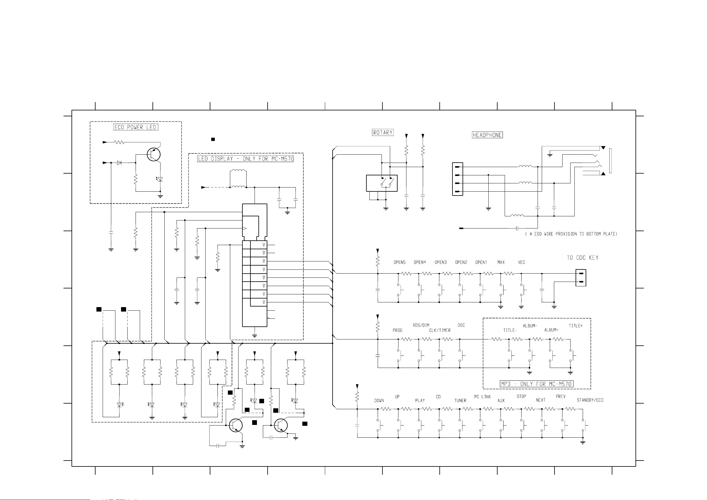
FRONT BOARD - CIRCUIT DIAGRAM (Part 2)
6-5
6-5
A
B
C
D
1301 A7
1302 A9
1303 A5
1304 D7
1305 D7
1306 D7
1307 D6
1308 D6
1309 F6
1310 F6
[4.9V
+C
+5V6
4406
MAXLit
AuxLit
1311 F8
1312 E6
1313 F6
1314 E7
1315 F8
1316 F9
1317 E9
1318 E8
1319 E9
1320 E8
1321 F7
1322 F7
1323 F8
1324 F7
1325 E7
1326 D8
1327 D8
1328 F9
1330 E6
2302 B6
2303 B6
2304 B8
2305 B8
2306 B8
2307 E5
2308 F5
2309 D5
2310 D8
2457 D2
2458 D2
2459 B4
2460 B4
2469 F4
2470 F3
2473 C1
3300 A1
3301 B1
3304 E1
3305 E1
3306 E1
3307 E2
3308 E2
3309 E2
3310 E2
3311 E3
3312 E3
3313 E3
3314 E4
3315 E4
3316 A6
3317 A6
3318 C5
3319 C6
3320 C7
3321 C7
3322 C7
3323 D5
3324 D6
3325 D6
3326 D7
3328 C8
3329 D7
3330 D8
3331 D8
3332 D9
3334 F9
3335 E5
3336 F6
3337 F6
3338 F6
3339 F7
3340 F7
3341 F7
3342 F8
3343 F8
3344 F8
3345 C6
3346 E3
3347 E4
3528 C1
3529 C2
3530 C2
3531 C3
4403 F3
4404 F4
4406 D1
4407 D1
5300 A8
5301 B8
5302 B8
5401 B3
5410 A3
6300 A1
6301 B2
6302 F1
6303 F1
6304 F2
6305 F3
6306 E3
6307 E4
7406 A2
7407 B3
7408 F3
7409 F4
8100 C9
8101 B7
9405 B3
123456789
Front Board
Circuit Diagram (Part 2)
1302
TC38
4
2
7
1
6
3
5
8100
CDCKEY2
1319
]
2473
3300
820R
6300
1N4148
100n
USB
LedShData
USBLit
4407
[0V
3301
3528
]
47K
10K
D
LedShClk
[1.9V
[1.7V
6301
TunerLit
BC857B
7406
]
LedEnable
]
ADC
3529
2457
10K
D
100p
D
LedShStr
CDLit
DC Voltages During Active Play.
Note :
Values in Bracket are DC Voltages at Standby (Clock Mode).
Values in Square Bracket are DC Voltages at Low Power Standby.
Note : Some values may varies, see respective parts list for correct value.
+5V6
Refer to Variant Table.Legend :
# For Provision Only .
5410
4u7
9405
5401
7407
74HC4094D
15
1
4u7
EN1
STB
5.6V
SRG8
16
2459
100n
2460
D
3
3530
10K
2
D1
4
5
D
3531
10K
D
6
7
14
13
2458
100p
D
12
11
9
10
8
LedShClk
PCLinkLit
LedShData
+5V6+5V6
MAXLit
D
+5V6 +5V6
USBLit
100n
MAXLit
USBLit
CDLit
TunerLit
AuxLit
PCLinkLit
VOLB
VOLA
KEY2
KEY0
1303
EC12
MT14MT2
+C
3318
2309
+C
3323
2307
+D
+D
10K
3316
3
1
2
5
2302
D
2K7
3345
150R
100p
2K7
100p
1308
3324
150R
1312
10K
3317
1301
1
HP_LEFT
2
3
HP_RIGHT
4
HP_DET
10n
10n
2303
D
D
FE-ST-VK-N
HP
# 8101
3319
220R
RT-01T
3320
270R
1307
1306
1
390R
3321
1305
3322
560R
1304
3328
820R
5302
2u2
2306
100n
1327
5300
2u2
5301
2u2
2304
1326
ADC
3325
220R
1330
3326
270R
1314
3329
390R
1325
3330
560R
3331
820R
1320
2310
1318
22n
100p
HP
2305
22n
1
2
35022
DD
3332
1K2
1317
A
B
C
D
E
F
3347
22p
10K
3314
1.95V1.95V
4404
820R
6307
7409
BC847B
3315
USB
ADC
820R
KEY1
+C
3335
2308
2K7
100p
3304
820R
6302
3305
1.95V
AUX
820R
3306
820R
6303
3307
1.95V
ADC
820R
3308
820R
6304
3309
1.95V
CDTUNER
ADC
820R
3310
PCLINK
820R
6305
# 2470
22p
3311
820R
3346
10K
3312
6306
7408
BC847B
D
820R
4403
MAX
3313
820R
# 2469
12345
3336
150R
1310
3337
220R
1313
3338
270R
1309
3339
390R
1321
3340
560R
1322
3341
820R
1324
3342
1K2
1323
3343
1K8
ADC
1311
3344
2K7
1315
3334
4K7
D
1316
1328
ADC
3139 118 56320...8239 210 94032 for 3501 pt2 dd wk0251
6789
E
F
Page 18
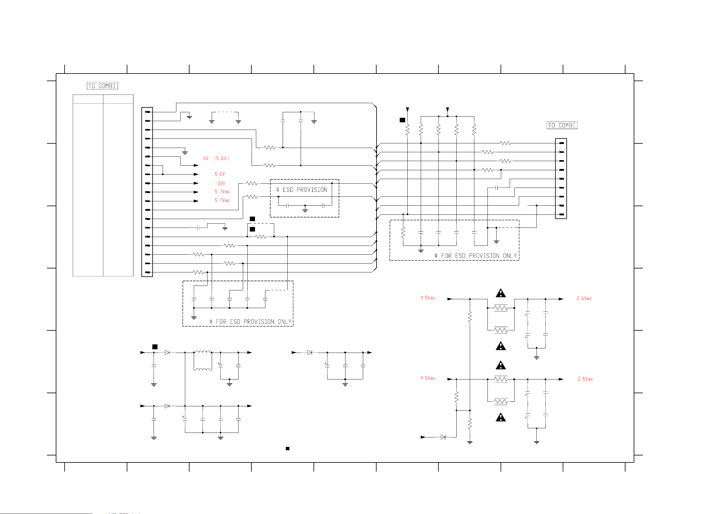
FRONT BOARD - CIRCUIT DIAGRAM (Part 3)
6-6 6-6
A
B
C
D
E
F
123456789
Front Board
Circuit Diagram (Part 3)
MP3
TRAY_IIC_SDA
uP_DATA
uP_CLK
uP_FRAME
uC_RESET
NON-MP3
NTC
GND_IIC
IIC_DATA
IIC_CLK
GND_D
+5V6_ECO
+5V6
+5V6
-33V
F1
F2
TRAY_IRQ
TRAY_IIC_SCL
CD_GND
CD_SIDA
CD_SICL
CD_SILD
CD_RAB
CD_PORE
+5V6_ECO
1
2
3
4
5
6
7
8
9
10
11
12
13
14
15
16
17
18
19
FE-ST-VK-N
+5V6
1401
# 2480
# 2472
6405
1N4003
100n
D
6406
1N4003
100n
D
2439
I2C
D
2450
16V47u
+5V6_ECO
+5V6
-33V
F1
F2
2464
100n
3454
470R
3456
470R
47p
D
5402
4u7
5409
4u7
2468
2451
100n
I2C
9413
10p
2438
# 2481
CD
3453
470R
3455
470R
245216V47u
100n
D
10p
2437
D
2482
IIC
2453
100n
100n
3450
470R
3451
470R
10p
+H
+C
10p
10p
IIC
IIC_DATA
IIC_CLK
3448
220R
3449
220R
# 2446
# 2447
TRAY_IRQ
TRAY_IIC_SCL
2448
47p
4408
3452
470R
2449
47p
D
TRAY_IIC_SDA_CD_SIDA
CD_SICL__uP_DATA
CD_SILD__uP_CLK
CD_RAB__uP_FRAME
CD_PORE__uC_RESET
4409
10p
2454
+5V
+5V6
6403
1N4003
16V47u
100n
2463
2425
D
+5V
DC Voltages During Active Play.
Note :
Values in Bracket are DC Voltages at Standby (Clock Mode).
Values in Square Bracket are DC Voltages at Low Power Standby.
Note : Some values may varies, see respective parts list for correct value.
Refer to Variant Table.Legend :
# For Provision Only .
2478
NTC
+D
100n
TUSTEREO
TUCLK
TUDATA
TUCE
TUENABLE
SA_IN
PWDN
Standby
+5V
3548
+C
3547
47K
39K
3440
2433
-33V
10K
47p
D
BZX79-B5V6
3441
2434
F1
F2
6404
+D
10K
47p
3442
2435
3431
10K
47p
220R
3429
3433
3447
2436
FTD
220R
22K
10K
47p
3444
1K
3543
1K
2432
100p
TU
3430
6R8
3432
10R
3532
6R8
3533
10R
3443
1K
3445
1K
4405
2426
2427
2428
2429
50V 4u7
50V 4u7
# 2474
# 2475
1402
FE-ST-VK-N
220p
F1x
1
TU_STEREO
2
TU_CLK
3
TU_DATA
4
TU_ENABLE
5
TU_GND
6
SA_IN
7
POWER_DOWN
8
NC
9
LOW_PWR_CTRL
FTD
F2x
220p 220p
# 2476
50V 4u7
220p
# 2477
50V 4u7
FTD
3139 118 56320...8239 210 94032 for 3501 pt2 dd wk0251
A
B
C
D
E
F
1401 A2
1402 A8
2425 E5
2426 D8
2427 E8
2428 E8
2429 F8
2432 B7
2433 C6
2434 C6
2435 C7
2436 C7
2437 E3
2438 E3
2439 F2
2446 A4
2447 A4
2448 B4
2449 B5
2450 D3
2451 D3
2452 D3
2453 D3
2454 D4
2463 E5
2464 C3
2468 F3
2472 F2
2474 D8
2475 E8
2476 E8
2477 F8
2478 E5
2480 E2
2481 F3
2482 F3
3429 D7
3430 D8
3431 F7
3432 D8
3433 F7
3440 A6
3441 A6
3442 A7
3443 A8
3444 B7
3445 B8
3447 A7
3448 B4
3449 B4
3450 B4
3451 B4
3452 C4
3453 C3
3454 C3
3455 C3
3456 D3
3532 E8
3533 F8
3543 B7
3547 A6
3548 C6
4405 C8
4408 C4
4409 D4
5402 E3
5409 E3
6403 E4
6404 F7
6405 E2
6406 F2
9413 A3
123456789
Page 19

6-7 6-7
CDC KEY BOARD - COMPONENT LAYOUT
This assembly drawing shows a summary of all possible versions. For components used in a specific version see schematic diagram and respective parts list.
3139 113 3501 pt2 dd wk0251
CDC KEY BOARD - CHIP LAYOUT
This assembly drawing shows a summary of all possible versions. For components used in a specific version see schematic diagram and respective parts list.
VARIANT TABLE
Model / Version
Item No.
3346
3347
3413
3403 / 3534 1K8 1K8
3406
3418
3419 10K
3423 1K8 1K8 1K8
3437
MC-500/22
MC-500/25
100K
33K 15K15K33K
680K
MC-500/30
MC-500/33
MC-500/37
10K10K
10K10K
10K
10K
680K
MC-M570/22
100K 100K
MC-M570/21
MC-M570/33
MC-M570/37
10K
CDC KEY BOARD - CIRCUIT DIAGRAM
1331 A2
1332 A2
1333 A3
1334 A3
1335 A3
1336 A1
3350 A2
3351 A2
123
Note : Some values may varies, see respective parts list for correct value.
A
1
2
1336
3350
1K2
EH-B
3352 A2
3353 A3
3351
1K8
1331
3354 A3
3352
2K7
1332
3353
4K7
1333
3354
10K
1334
3139 113 3501 pt2 dd wk0251
A
1335
3438
3439
1M 2M2 2M2
1M
1M
1M
3452 470R 470R
3545 10K10K
3547 39K
4400
4403
4404
4408
X4406
X
X
X4407
XX
XX
XX
XX
6405 X X X
6407
7408
7409
XX
XX
XX
B
D
3139 118 56320...8239 210 94042 for 3501 pt2 dd wk0251
123
X - Item in use.
B
Page 20

6-8
6-8
ELECTRICAL PARTS LIST - FRONT BOARD
MISCELLANEOUS
1301 4822 265 11183 Flex Connector 4P
1302 2422 026 05059 Headphone Socket
1303 2422 129 16708 Rotary Encoder 24P
1304 4822 276 13775 Tact Switch
1305 4822 276 13775 Tact Switch
1306 4822 276 13775 Tact Switch
1307 4822 276 13775 Tact Switch
1308 4822 276 13775 Tact Switch
1309 4822 276 13775 Tact Switch
1310 4822 276 13775 Tact Switch
1311 4822 276 13775 Tact Switch
1312 4822 276 13775 Tact Switch
1313 4822 276 13775 Tact Switch
1314 4822 276 13775 Tact Switch
1315 4822 276 13775 Tact Switch
1316 4822 276 13775 Tact Switch
1321 4822 276 13775 Tact Switch
1322 4822 276 13775 Tact Switch
1323 4822 276 13775 Tact Switch
1324 4822 276 13775 Tact Switch
1325 4822 276 13775 Tact Switch
1326 4822 276 13775 Tact Switch
1327 4822 276 13775 Tact Switch
1328 4822 276 13775 Tact Switch
1330 4822 276 13775 Tact Switch
1331 4822 276 13775 Tact Switch
1332 4822 276 13775 Tact Switch
1333 4822 276 13775 Tact Switch
1334 4822 276 13775 Tact Switch
1335 4822 276 13775 Tact Switch
1400 4822 265 11535 Flex Connector 8P
1401 4822 265 11545 Flex Connector 19P
1402 4822 265 11531 Flex Connector 9P
1403 3139 110 53331 FTD (HNA-10LS02T)
CAPACITORS
2302 5322 126 11583 10nF 10% 50V
2303 5322 126 11583 10nF 10% 50V
2304 4822 126 14494 22nF 10% 25V
2305 4822 126 14494 22nF 10% 25V
2306 2238 586 59812 100nF 50V
2307 2020 552 94427 100pF 5% 50V
2308 2020 552 94427 100pF 5% 50V
2309 2020 552 94427 100pF 5% 50V
2310 2020 552 94427 100pF 5% 50V
2406 3198 017 41050 1uF 10V
2407 4822 126 13879 220nF +80/-20% 16V
2408 4822 126 11785 47pF 5% 50V /22/25
2409 4822 126 11785 47pF 5% 50V /22/25
2410 4822 126 14249 560pF 10% 50V /22/25
2411 4822 126 14249 560pF 10% 50V /22/25
2412 4822 124 22652 2,2uF 20% 50V /22/25
2413 2238 586 59812 100nF 50V
2415 2238 586 59812 100nF 50V /22/25
2416 5322 126 11578 1nF 10% 50V /22/25
2418 2222 867 15339 33pF 5% 50V
2419 4822 122 33761 22pF 5% 50V
2420 4822 122 33761 22pF 5% 50V
2421 4822 126 14223 2,2pF 50V
2422 5322 126 11583 10nF 10% 50V
2423 3198 017 44740 470nF 10V
2424 5322 126 11583 10nF 10% 50V
2425 4822 124 81286 47uF 20% 16V
2426 4822 124 12032 4,7uF 20% 50V
2427 4822 124 12032 4,7uF 20% 50V
2428 4822 124 12032 4,7uF 20% 50V
2429 4822 124 12032 4,7uF 20% 50V
2432 2020 552 94427 100pF 5% 50V
2437 2238 586 59812 100nF 50V
2438 4822 124 81286 47uF 20% 16V
2439 4822 124 81286 47uF 20% 16V
2455 2238 586 59812 100nF 50V
2456 4822 122 33761 22pF 5% 50V
2461 3198 028 52290 22uF 20% 50V
2462 3198 028 52290 22uF 20% 50V
2463 2238 586 59812 100nF 50V
2464 2238 586 59812 100nF 50V
2466 4822 126 14238 2,2nF 50V
2467 4822 124 12032 4,7uF 20% 50V
2468 2238 586 59812 100nF 50V
2471 3198 017 34730 47nF 16V /22/25
2473 2238 586 59812 100nF 50V
2478 2238 586 59812 100nF 50V
2482 2238 586 59812 100nF 50V
RESISTORS
3300 4822 116 52231 820R 5% 0,5W /22/25
3301 4822 117 12925 47k 1% 0,063W /22/25
3312 4822 117 12968 820R 5% 0,62W
3313 4822 117 12968 820R 5% 0,62W
3314 4822 117 12968 820R 5% 0,62W
3315 4822 117 12968 820R 5% 0,62W
3316 4822 051 30103 10k 5% 0,062W
3317 4822 051 30103 10k 5% 0,062W
3318 4822 051 30272 2k7 5% 0,062W
3319 4822 051 30221 220R 5% 0,062W
3320 4822 051 30271 270R 5% 0,062W
3321 4822 051 30391 390R 5% 0,062W
3322 4822 051 30561 560R 5% 0,062W
3323 4822 051 30272 2k7 5% 0,062W
3324 4822 051 30151 150R 5% 0,062W
3325 4822 051 30221 220R 5% 0,062W
3326 4822 116 83876 270R 5% 0,5W
3328 4822 117 12968 820R 5% 0,62W
ELECTRICAL PARTS LIST - FRONT BOARD
3334 4822 116 52283 4k7 5% 0,5W
3335 4822 051 30272 2k7 5% 0,062W
3336 4822 051 30151 150R 5% 0,062W
3337 4822 051 30221 220R 5% 0,062W
3338 4822 116 83876 270R 5% 0,5W
3339 4822 051 30391 390R 5% 0,062W
3340 4822 051 30561 560R 5% 0,062W
3341 4822 117 12968 820R 5% 0,62W
3342 4822 117 11817 1k2 1% 1/16W
3343 4822 117 12903 1k8 1% 0,063W
3344 4822 051 30272 2k7 5% 0,062W
3345 4822 051 30151 150R 5% 0,062W
3346 4822 051 30103 10k 5% 0,062W
3347 4822 051 30103 10k 5% 0,062W
3350 4822 117 11817 1k2 1% 1/16W
3351 4822 117 12903 1k8 1% 0,063W
3352 4822 051 30272 2k7 5% 0,062W
3353 4822 051 30472 4k7 5% 0,062W
3354 4822 051 30103 10k 5% 0,062W
3403 4822 117 12903 1k8 1% 0,063W
3404 4822 051 30684 680k 5% 0,062W
3405 4822 051 30474 470k 5% 0,062W
3406 4822 051 30333 33k 5% 0,062W
3407 4822 051 30152 1k5 5% 0,062W /22/25
3408 4822 051 30103 10k 5% 0,062W /22/25
3409 4822 051 30222 2k2 5% 0,062W /22/25
3410 4822 117 12891 220k 1% /22/25
3413 4822 117 13632 100k 1% 0,62W /22/25
3416 4822 051 30102 1k 5% 0,062W /22/25
3417 4822 051 30102 1k 5% 0,062W /22/25
3418 4822 050 21003 10k 1% 0,6W /30/37
3419 4822 051 30103 10k 5% 0,062W /30/37
3420 4822 051 30272 2k7 5% 0,062W
3421 4822 051 30102 1k 5% 0,062W
3422 4822 051 30684 680k 5% 0,062W
3423 4822 116 52249 1k8 5% 0,5W /22/25
3424 4822 117 12891 220k 1%
3425 4822 051 30682 6k8 5% 0,062W
3426 4822 051 30102 1k 5% 0,062W
3427 4822 051 30102 1k 5% 0,062W
3428 4822 051 30682 6k8 5% 0,062W
3429 4822 116 83872 220R 5% 0,5W
!
3430 4822 052 10688
6R8 5% 0,33W
3431 4822 116 83872 220R 5% 0,5W
3432 4822 052 10109!10R 5% 0,33W
3433 4822 116 52257 22k 5% 0,5W
3437 4822 051 30684 680k 5% 0,062W
3438 4822 051 30105 1M 5% 0,062W
3439 4822 051 30105 1M 5% 0,062W
3440 4822 051 30103 10k 5% 0,062W
3441 4822 051 30103 10k 5% 0,062W
3442 4822 051 30103 10k 5% 0,062W
3443 4822 051 30102 1k 5% 0,062W
3444 4822 051 30102 1k 5% 0,062W
3445 4822 051 30102 1k 5% 0,062W
3447 4822 051 30103 10k 5% 0,062W
3448 4822 116 83872 220R 5% 0,5W
3449 4822 116 83872 220R 5% 0,5W
3450 4822 051 30471 470R 5% 0,062W
3451 4822 051 30471 470R 5% 0,062W
3453 4822 116 83883 470R 5% 0,5W
3454 4822 116 83883 470R 5% 0,5W
3455 4822 051 30471 470R 5% 0,062W
3456 4822 051 30471 470R 5% 0,062W
3457 4822 051 30471 470R 5% 0,062W
3458 4822 051 30102 1k 5% 0,062W
3459 4822 051 30102 1k 5% 0,062W
3460 4822 051 30102 1k 5% 0,062W
3461 4822 051 30471 470R 5% 0,062W
3462 4822 051 30102 1k 5% 0,062W
3463 4822 051 30472 4k7 5% 0,062W
3464 4822 051 30102 1k 5% 0,062W
3465 4822 051 30102 1k 5% 0,062W
3466 4822 116 52175 100R 5% 0,5W
3467 4822 116 52175 100R 5% 0,5W
3468 4822 116 52175 100R 5% 0,5W
3469 4822 116 52175 100R 5% 0,5W
3470 4822 050 11002 1k 1% 0,4W
3471 4822 050 11002 1k 1% 0,4W
3472 4822 051 30102 1k 5% 0,062W
3473 4822 051 30471 470R 5% 0,062W
3474 4822 051 30471 470R 5% 0,062W
3475 4822 051 30471 470R 5% 0,062W
3476 4822 051 30102 1k 5% 0,062W
3477 4822 051 30102 1k 5% 0,062W
3478 4822 051 30102 1k 5% 0,062W
3479 4822 051 30102 1k 5% 0,062W
3480 4822 051 30102 1k 5% 0,062W
3481 4822 051 30102 1k 5% 0,062W
3482 4822 050 11002 1k 1% 0,4W
3483 4822 050 11002 1k 1% 0,4W
3484 4822 051 30102 1k 5% 0,062W
3485 4822 051 30102 1k 5% 0,062W
3486 4822 051 30102 1k 5% 0,062W
3487 4822 051 30102 1k 5% 0,062W
3489 4822 051 30102 1k 5% 0,062W
3490 4822 051 30102 1k 5% 0,062W
3491 4822 051 30102 1k 5% 0,062W
3492 4822 051 30102 1k 5% 0,062W
3493 4822 051 30102 1k 5% 0,062W
3494 4822 051 30102 1k 5% 0,062W
3495 4822 051 30102 1k 5% 0,062W
3496 4822 051 30102 1k 5% 0,062W
3497 4822 051 30102 1k 5% 0,062W
Page 21

6-9
6-10
ELECTRICAL PARTS LIST - FRONT BOARD
RESISTORS
3498 4822 051 30102 1k 5% 0,062W
3499 4822 051 30102 1k 5% 0,062W
3500 4822 051 30102 1k 5% 0,062W
3501 4822 051 30102 1k 5% 0,062W
3502 4822 051 30102 1k 5% 0,062W
3503 4822 051 30102 1k 5% 0,062W
3504 4822 051 30102 1k 5% 0,062W
3505 4822 051 30102 1k 5% 0,062W
3506 4822 051 30102 1k 5% 0,062W
3507 4822 051 30102 1k 5% 0,062W
3508 4822 051 30102 1k 5% 0,062W
3509 4822 051 30102 1k 5% 0,062W
3510 4822 051 30102 1k 5% 0,062W
3511 4822 051 30102 1k 5% 0,062W
3512 4822 051 30102 1k 5% 0,062W
3513 4822 051 30102 1k 5% 0,062W
3514 4822 051 30102 1k 5% 0,062W
3515 4822 051 30102 1k 5% 0,062W
3516 4822 051 30102 1k 5% 0,062W
3517 4822 051 30102 1k 5% 0,062W
3518 4822 051 30102 1k 5% 0,062W
3519 4822 051 30102 1k 5% 0,062W
3520 4822 051 30102 1k 5% 0,062W
3521 4822 051 30102 1k 5% 0,062W
3522 4822 051 30102 1k 5% 0,062W
3523 4822 051 30102 1k 5% 0,062W
3524 4822 051 30102 1k 5% 0,062W
3525 4822 051 30102 1k 5% 0,062W
3526 4822 051 30471 470R 5% 0,062W
3527 4822 051 30471 470R 5% 0,062W
3528 4822 051 30103 10k 5% 0,062W
3532 4822 052 10688
3533 4822 052 10109
!
6R8 5% 0,33W
!
10R 5% 0,33W
3534 4822 117 12903 1k8 1% 0,063W
3536 4822 051 30472 4k7 5% 0,062W
3537 4822 051 30472 4k7 5% 0,062W
3538 4822 116 52175 100R 5% 0,5W
3539 4822 051 30103 10k 5% 0,062W
3540 4822 051 30102 1k 5% 0,062W
3543 4822 051 30102 1k 5% 0,062W
3545 4822 051 30103 10k 5% 0,062W
3547 4822 051 30393 39k 5% 0,062W /22/25
4300 4822 051 30008 0R Jumper 0603
4301 4822 051 30008 0R Jumper 0603
4302 4822 051 30008 0R Jumper 0603
4402 4822 051 30008 0R Jumper 0603
4406 4822 051 30008 0R Jumper 0603
4407 4822 051 30008 0R Jumper 0603
4408 4822 051 30008 0R Jumper 0603
4410 4822 051 30008 0R Jumper 0603
4411 4822 051 30008 0R Jumper 0603
4420 4822 051 30008 0R Jumper 0603
4421 4822 051 30008 0R Jumper 0603
4422 4822 051 30008 0R Jumper 0603
4423 4822 051 30008 0R Jumper 0603
4424 4822 051 30008 0R Jumper 0603
4425 4822 051 30008 0R Jumper 0603
4426 4822 051 30008 0R Jumper 0603
4427 4822 051 30008 0R Jumper 0603
4428 4822 051 30008 0R Jumper 0603
4429 4822 051 30008 0R Jumper 0603
4430 4822 051 30008 0R Jumper 0603
4431 4822 051 30008 0R Jumper 0603
4432 4822 051 30008 0R Jumper 0603
4433 4822 051 30008 0R Jumper 0603
4434 4822 051 30008 0R Jumper 0603
4435 4822 051 30008 0R Jumper 0603
4436 4822 051 30008 0R Jumper 0603
4437 4822 051 30008 0R Jumper 0603
4438 4822 051 30008 0R Jumper 0603
4439 4822 051 30008 0R Jumper 0603
4440 4822 051 30008 0R Jumper 0603
4441 4822 051 30008 0R Jumper 0603
4442 4822 051 30008 0R Jumper 0603
4443 4822 051 30008 0R Jumper 0603
4444 4822 051 30008 0R Jumper 0603
4445 4822 051 30008 0R Jumper 0603
4446 4822 051 30008 0R Jumper 0603
4447 4822 051 30008 0R Jumper 0603
4448 4822 051 30008 0R Jumper 0603
4449 4822 051 30008 0R Jumper 0603
4450 4822 051 30008 0R Jumper 0603
4451 4822 051 30008 0R Jumper 0603
4452 4822 051 30008 0R Jumper 0603
4453 4822 051 30008 0R Jumper 0603
4454 4822 051 30008 0R Jumper 0603
4455 4822 051 30008 0R Jumper 0603
4456 4822 051 30008 0R Jumper 0603
4457 4822 051 30008 0R Jumper 0603
4458 4822 051 30008 0R Jumper 0603
4459 4822 051 30008 0R Jumper 0603
4460 4822 051 30008 0R Jumper 0603
4461 4822 051 30008 0R Jumper 0603
4462 4822 051 30008 0R Jumper 0603
COILS & FILTERS
5300 3198 018 52280 FXD IND 2,2uH 10%
5301 3198 018 52280 FXD IND 2,2uH 10%
5302 3198 018 52280 FXD IND 2,2uH 10%
5402 3198 018 54780 FXD IND 4,7uH 10%
5403 2422 543 01069 RES XTL 32,768kHz
5404 5322 242 73686 RES CER 12MHz
5405 4822 242 11033 RES XTL 4,332MHz /22/25
5406 3198 018 52280 FXD IND 2,2uH 10% /22/25
ELECTRICAL PARTS LIST - FRONT BOARD
COILS & FILTERS
5407 3198 018 52280 FXD IND 2,2uH 10%
5408 3198 018 54780 FXD IND 4,7uH 10%
5409 3198 018 54780 FXD IND 4,7uH 10%
5411 3198 018 54780 FXD IND 4,7uH 10%
DIODES
6300 4822 130 30621 1N4148 /22/25
6301 9322 179 76676 LED VS LTL-816EELC/22/25
6306 9322 178 15676 LED VS LTL-8166FTNN
6307 9322 178 15676 LED VS LTL-8166FTNN
6401 4822 130 30621 1N4148
6403 4822 130 31878 1N4003G
6404 4822 130 83206 BZX79-B5V6
6405 4822 130 31878 1N4003G /22/25
6406 4822 130 31878 1N4003G
6408 4822 130 30621 1N4148
6409 4822 130 30621 1N4148
6410 4822 130 30621 1N4148
TRANSISTORS & INTEGRATED CIRCUITS
7301 9322 185 97667 IR Receiver TSOP4836ZC1
7400 3139 110 53381 TMP88CU74YF - ‘500S53381’
7401 9322 145 26668 M24C02-WMN6
7403 9352 686 05118 SAA6581T /22/25
7404 5322 130 60159 BC847B
7405 5322 130 60159 BC847B
7406 4822 130 60373 BC857B /22/25
7408 5322 130 60159 BC847B
7409 5322 130 60159 BC847B
Note : Only the parts mentioned in this list are normal
service spare parts.
Page 22

7A-17A-1
1
FM
Osc.
FM
Mixer
AM
Mixer
AM
Osc.
AM IF
IF1
IF2
FM
Det.
AM
Det.
3393733
RADIO IC
TEA 5757H
TUNER BOARD
ECO 6
Systems
1018 11
14
15
24
right
right
left
left
stereo
VCO
4140 36 193244 25
Stereo
Decoder
AFC
AFC +
AFC -
4
4
AGC
Pre-
scaler
Multi-
plexer
Charge
pump
Stabilizer
CONTROL
Reference
Oscillator
29
28
27
clock
data
enable
P1
P0
31
30
programmable
output ports
V
Loop
V
Loop
V
Loop
V
Loop
V
Loop
2
6
5
43
C
D
450kHz450kHz450kHz
20
75kHz
V
Stab
AV
Stab
BV
Stab
B
V
Stab
A V
Stab
B
10,7 MHz 10,7 MHz
35 9
Vdd Vcc1
723
V
Stab
A
V
Stab
B
38
34
22
Vcc2
8
ECO6 Systems, 140499
LF filter
RDS
(MPX)
RDS
(MPX)
stereo
clock
data
enable
Version
1120
1
8
FM
Frontend
AM
Frontend
AM-FRAME AERIAL
B
1103
1101
(1102)
A
FM
MPX
buffer ampl.
5
Discriminator
10,7 MHz
Vdd
Vcc1
Vcc
Vcc2
AM-RF
AM-Osc.
FM-Osc.
FM-RF FM-IF 1 FM-IF 2
AM-IF 1 AM-IF 2
AM-AFC
3
2
BLOCK DIAGRAM
ECO6 Tuner Board
version:
SYSTEMS non-CENELEC
TABLE OF CONTENTS
Blockdiagram ..................................................................7A-1
Schematic Diagram.........................................................7A-2
Component Layout..........................................................7A-3
Adjustment table .............................................................7A-3
Electrical Partslist............................................................7A-4
Page 23

7A-2 7A-2
ECO6 Sys-non Cenelec, 000911
1101 A1
1102 B1
1103 F2
1120 E14
1130 A2
1131 B2
1132 G13
2101 B3
2102 B1
2103 C7
2104 B3
2105 A2
2106 F3
2107 F4
2119 H6
2120 G6
2124 H6
2125 H6
2126 F7
2127 E7
2128 C8
2129 C7
2130 F11
2131 G8
2132 G8
2133 G8
2134 H8
2135 H9
2136 G14
2137 G13
2138 F9
2139 G9
2140 G9
2141 F10
2143 G12
2144 G11
2145 F12
2146 E12
2147 E12
2148 E12
2149 H7
2150 A10
2152 E4
2153 E5
2154 D5
2155 D5
2159 F6
2161 C11
2163 D11
2164 F10
2165 C7
2166 E11
2167 E11
2169 H8
3101 E4
3102 D4
3103 C6
3104 A7
3105 B6
3132 G5
3134 H6
3141 E7
3142 E7
3143 G7
3144 H7
3145 F8
3146 G13
3152 G14
3153 G13
3154 G13
3155 G11
3156 C12
3157 C12
3158 E13
3159 D13
3160 D12
3161 D13
3167 F12
3168 F11
3169 E11
3170 C12
3172 G12
3176 G7
3181 E6
5102 F2
5109 B9
5110 B10
5111 A8
5112 A11
5114 B11
5119 G9
5121 E11
5123 G5
5130 E5
5131 C6
6103 B2
6105-1 F3
6105-2 G5
6106 C3
6107 G13
6120 C13
6130 E5
6131 D5
7101 C8
7102 C6
7103 H7
7111 C13
7112 G12
T102 B2
T103 B2
T105 F2
T106 F2
T109 B6
T110 F5
T111 F4
T112 F7
T113 A8
T114 B10
T115 A8
T116 F10
T117 G13
T118 G11
T120 F13
T121 F13
T122 F13
T123 E13
T124 G14
T125 F14
T126 F13
T127 F13
T128 D7
T140 F11
T141 F10
T142 F10
1
34
6
87
2
1
34
6
87
2
LEGEND
p ...for provision only
USA ... for USA version only
E-EU ... for East European version only
22n
USA
22n
USA
p
p
p
7
1
2
3
8
6105
6
HN1V02H
54
3
6
1
2
7
29
25
13
30
31
16
4
42
15
1
7
22
9
23
38 34
2118
37 35
33
43 39
5
3
8
171412
24
11
10
2019
44
32
41 3640
6
2
27
28
26
1
3
4
5
6
87
2
1
34
6
87
2
1
34
6
87
2
p
SCALER
MULTI-
PLEXER
CONTROL
FILTER
AM
IF
AM
DET
FM
DET
VSTABB
DECODER
CHARGE
PUMP
AGC
OSC
AM DET
FM
IF2
RIPPLE
AGC
STABILIZER
AFC
VDD
VSTABA
AM-IF
MONO/
FM
FRONTEND
CONTROL
XTAL
AGC
PRE-
CTRL
AGC
AM
OSC
AGC
VCC2
FM
OSC
AM
MIXER
MIXER
FM
FM
IF1
FRONTEND
AM
STEREO
STEREO
RDS only
DISCRIMINATOR
to/from
FM-OSCILLATOR
PROGR.
MPX
Q-multiplier
MW
OUTPUT PORTS
to 1120
pin 5
ENABLE/MPX
BUFFER
kHz
VERSION DETECTION
VCO
RIGHT
14
12 3
AM FRAME AERIAL
DATA
C
D
E
F
AM-OSCILLATOR
FM 75 OHM
FM-IF2
MW
2345
AM-RF
450kHz
450kHz
AM-IF2
from 2169
78
AM-AFC
LEFT
6 7 8 9 10 11 12 13
456
FM-RF
TUNER BOARD ECO6
/ SYSTEMS NON CENELEC
9 1011121314
A
B
G
H
A
B
1
VCC
STEREO
CLOCK
AMPLIFIER
GND
H
C
D
E
F
G
470n
2132
BAS216
6120
2103
1u
2107
1n
3134
22K
6105-2
HN1V02H
100n
2163
T141
7KL
1K
3144
5102
3157
100K
T109
470R
3153
2130
22n
220R
3105
3142
100K
3167
120R
33p
2149
2K2
3145
1132
C-PAD
T103
T111
2164
470n
T102
2140 15p
2139
2138
2u2
82p
2133
1u
3103
8K2
T120
4p7
2154
3156
1101
USA
YKD21
100K
2161
100n
5119
2119
10p
T142
5123
11p
2106
3172
6106
BAS216
100n
2165
5K6
3154
3155
220R
330R
2124
33K
3176
22n
WRITE-EN
5114
7P
MUTE
P0
P1
PILOT
RF-GND1
RF-GND2
RIGHT
RIPPLE
VCC1
VCC2
VCO
VDD
VSTABA
VSTABB
FM-DEMOD
FM-IF1-IN
FM-IF2
FM-IF2-IN
FM-IN
FM-MIXOUT
FM-OSC
FM-RF
I-TUNE
IF-GND
LEFT
LPF
MPX-IN
AF-OUT
AFC+
AFC-
AGC
AM-AFC
AM-IF1-IN
AM-IF2
AM-MIXOUT
AM-OSC
AM-RF
CLOCK
DATA
DIG-GND
FIELDSTR-IND
5130
T127
T126
220n
2127
5121
DT-381
150K
3169
75K
3102
100K
56K
3141
1131
C-PAD
3132
5112
7P
6107
47R
6131
1SV228
BZX284-C11
1120
FE-BT-VK-N
T118
T140
T117
T112
2131
470n
33K
3101
1SV228
6130
3168
120R
2125
560p
T116
2n2
2148
100n
2141
470R
18p
2120
470R
3158
3152
3159
XH-S
1103
3160
470R
470R
220n
2143
2150
T125
1
2
3
4
5
6
7
8
22R
3146
BF550
7102
5131
11p
2155
O
100K
5110
G
I
1102
not USA
3170
T122
2135
15n
2167
2145
220p
T110
12p
HN1V02H
1n
2166
T105
6105-1
T106
T121
T123
BC547C
7112
3143
2129
100u
C-PAD
1130
22K
220n
2137
T128
3181
1K
330p
2126
2101
47p
BAV99
6103
2104
100p
2153
15p
T124
2152
33n
560p
E-EU
12p
E-EU
2p2
J
33p
2159
220p
2146
2169
2n2
1u
15n
2134
2144
220n
2136
22K
3161
BC857C
BC847C
7111
7103
2147
220p
VCC2
VCC2
VDD
T114
MPX
P1
P0
P1
VDD
MPX
VCC1
VCC1
VCC1
printed
printed
printed
1
2
13
2
1
2
3
1
2
TEA5757H
TEA5759H
J
7101
2128
10u
7111
component mounted
/14 FM-OIRT/MW
/00 /02 FM/MW/LW
6120 3170
/01 FM/MW
VERSION
/00 /02 FM/MW
3156
/17 FM/AM
/06 FM-Japan/AM
3157
VERSION PROGRAMMING COMPONENTS
J ... for Japanese version only
AM-IF1
450kHz
8
5111
1
2
3
4
6
7
T113
T115
FM-IF1
2
G
1I3
O
5109
3104
330R
100n
0R
4103
...V MW mode
...V LW mode
voltages measured while
set is tuned to a strong transmitter
...V FM mode stereo
EVM
V
5V
0V
152kHz, 50mV
pp
stereo stereomono
9.6V
9.5V
9.5V
10.4V
12V
1V
1.3V
1.4V
stereo 0.2V
mono 4.8V
9.6V
12Vtyp
stereo 0.4V
0.15V
11.1V
7.8V
2V
0.7V
0V
1.2V
7.6V
(10-14V)
0.2V
0V
1.2V
0.1V
D
1.4V
0.7V
4
0V
0V
mono 4.8V
1.4V
9.6V
1.4V
0.2V
0.7V
1.4V
7.9V
7.7V
0V
0V
0V
0V
0.6V
0.8V
0.1V
1.6-8V
1-8V
11.1V
0V
1V
1.4V
1.4V
B
7.6V
5
3
2
A
1.3V
0.7V
7.8V
11.1V
0.8V
0.6V
0.6V
1V
0.7V
1V
1.1V
1.1V
0V
0V
2V
C
1
0.8V
1.2V
1.1V
IF-AMP.
BFS20
7119
J
1K
3113
J
2112
J
100p
330R
3119
J
Signal path
FM
AF - left/right
AM
MPX (Audio Frequency)
2102
100n
2105
USA
100n
Page 24

7A-37A-3
VARICAP ALIGNMENT
FM RF
FM IF
VCO
AM IF
AM RF
3)
108MHz
87.5MHz
(65.81MHz)
87.5MHz
(65.81MHz)
87.5MHz
(65.81MHz)
279kHz
153kHz
1602kHz
531kHz
5130
check
5122
check
5123
check
8V ±0.2V
4.3V ±0.5V
(1.2V ±0.5V)
8V ±0.2V
1.1V ±0.4V
8V ±0.2V
1.1V ±0.4V
1494kHz
558kHz
560kHz 5102
1500kHz
5103198kHz
1494kHz
558kHz
560kHz
1500kHz
198kHz
2106
5102
2106
3142 152kHz ±1kHz
1)
98MHz
5112
MAX
FM
87.5 - 108MHz
(65.81 - 74, 87.5 - 108MHz)
LW
153 - 279kHz
MW
FM/MW/LW- version, 9kHz grid
531 - 1602kHz
1700kHz
530kHz
5123
check
8V ±0.2V
1.1V ±0.4V
1602kHz
531kHz
5123
check
6.9V ±0.2V
1.1V ±0.4V
108MHz
108MHz 2155
5131
MW
FM/AM-version, 10kHz grid
530 - 1700kHz
FM
MW
LW
98MHz, 1mV
continuous wave
450kHz
connect pin 6 of
IC 7101 (AM Osc.)
with 3.3kΩ to Vcc
Use Service Testprogram. By selecting the TUNER TEST test frequencies will be stored as preset frequencies automatically.
4
1
3
5
5
A
A
5119FM
10.7MHz, 45mV
continuous wave
2D
mod=1kHz
∆f=±22.5kHz
1)
If sensitivity of frequency counter is too low adjust to max. channel separation
(input signal: stereo left 90% + 9%, adjust output on right channel to minimum)
Repeat
ECO6, Sys + PA with frame aerial, 070799
TUNER ADJUSTMENT TABLE ( ECO6 FM/MW- and FM/MW/LW - versions with AM-frame aerial )
∆f=±10kHz
VRF = 0.5mV
C
see
remark
2)
220R
100nF
36
IC 7101
220R
100nF
40
IC 7101
2141
shortcircuit
to block AFC
21
IC 7101
max.
symmetric
f
o
AM AFC
MW
C
continuous wave
VRF = 2mV
5111
5114
2
0 ± 2 mV DC
0 ± 3 mV DC
MW
4)
FM/MW/LW- and FM/MW-version
( 9kHz grid)
531 - 1602kHz
B
∆f = ±30kHz
V
RF
as low as
possible
max.
symmetric
f
o
MW
FM/AM-version, 10kHz grid
530 - 1700kHz
3)
For AM RF adjustments the original frame antenna has to be used !
2)
RC network serves for damping the IF-filter while adjusting the other one.
4)
MW has to be aligned before LW.
Waverange Input frequency Input Tuned to Adjust Output Scope/Voltmeter
FM
87.5 - 108MHz
(65.81 - 74, 87.5 - 108MHz)
FM/MW-version, 9kHz grid
531 - 1602kHz
(as low as
possible)
ECO6 System non Cenelec stage .3, 120900
TUNER BOARD ECO6
Systems non Cenelec
/ componentside view
1101 A6
1102 B6
1103 D6
1120 A4
1130 B5
1131 D5
1132 A5
2106 C5
2107 B5
2128 C4
2129 B4
2133 D2
2138 C2
2144 B2
2155 C4
3142 D2
5102 D6
5109 A3
5110 B3
5111 B4
5112 A3
5114 A2
5119 C2
5121 B2
5123 D5
5130 D3
5131 D4
7112 C1
9101 A2
9103 B2
9104 B5
9105 B1
9106 B3
9107 D4
9108 C4
9109 D2
AM FRAME AERIAL
FM 75Ω
B
A
TUNER BOARD ECO6
Systems - non Cenelec
/
copperside view
2101 B4
2102 B1
2103 D4
2104 B4
2105 C1
2112 B5
2119 D3
2120 D3
2124 D3
2125 D3
2126 D6
2127 C5
2130 D5
2131 C5
2132 D6
2134 D7
2135 D7
2136 A4
2137 A4
2139 C6
2140 C6
2141 C6
2143 C7
2145 A5
2146 B7
2147 A5
2148 B6
2149 D6
2150 B5
2152 C5
2153 C5
2154 C4
2159 C5
2161 A6
2163 B6
2164 C6
2165 C4
2166 B6
2167 B6
2169 A4
3101 D5
3102 C3
3103 C4
3104 B4
3105 C4
3113 B5
3119 B5
3132 D5
3134 D3
3141 C5
3143 D6
3144 B7
3145 C5
3146 C7
3152 A4
3153 A4
3154 C7
3155 C7
3156 A6
3157 A6
3158 A4
3159 A5
3160 A5
3161 A5
3167 B7
3168 C7
3169 B6
3170 A6
3172 C7
3176 D6
3181 D4
4103 B5
4106 C4
4107 C5
4108 C5
6103 B3
6105 C3
6106 C3
6107 C7
6120 A6
6130 D4
6131 C4
7101 C5
7102 D4
7103 D7
7111 A5
7119 B5
These assembly drawings show a summary of all possible versions.
For components used in a specific version see schematic diagram respectively partslist.
ECO6 Systems non CENELEC stage .3, 120900
41..
in schematic diagram)
(not all items shown
SMD jumper
EB
C
A
K
1
2
7
8
4
D
A
C
1
2
5
3
V
dd
Vcc2
Vcc1
Page 25

MISCELLANEOUS
–––––––––––––––––––––––––––––––––––––––––––––––––––––
1101 2422 015 19376 SOCKET 2P CLICKFIT USA only
1102 4822 267 10283 SOCKET COAX, IEC 75Ω not USA
1103 4822 265 31184 JST CONNECTOR 2 POLE
1120 4822 265 11515 FFC SOCKET, 8P
CAPACITORS
–––––––––––––––––––––––––––––––––––––––––––––––––––––
2101© 4822 126 13692 47pF 1% 63V
2102© 4822 126 13838 100nF 10% 50V not USA
2103© 5322 122 31647 1nF 10% 63V
2104© 5322 122 32531 100pF 5% 50V
2105© 4822 126 13838 100nF 10% 50V USA only
2106 2020 800 00191 3-11pF TRIMCAP.,N450
2107 4822 121 51319 1µF 20% 50V
2120© 4822 126 13689 18pF 1% 63V
2124© 5322 122 32654 22nF 10% 63V
2125© 2020 552 96199 560pF 1% 50V
2126© 5322 122 31863 330pF 5% 50V
2127© 4822 126 14076 220nF 20% 25V
2128 4822 124 40248 10µF 20% 63V
2129 4822 124 41584 100µF 20% 10V
2130© 5322 122 32654 22nF 10% 63V
2131© 4822 126 13482 470nF 20% 16V
2132© 4822 126 13482 470nF 20% 16V
2133 4822 124 21913 1µF 20% 63V
2134© 4822 126 13188 15nF 5% 63V not USA
2134© 5322 122 32654 22nF 10% 63V USA only
2135© 4822 126 13188 15nF 5% 63V not USA
2135© 5322 122 32654 22nF 10% 63V USA only
2136© 4822 126 14076 220nF 20% 25V
2137© 4822 126 14076 220nF 20% 25V
2138 4822 124 22652 2,2µF 20% 50V
2139© 4822 126 14236 15pF 5% 50V
2140© 4822 126 13695 82pF 1% 63V
2141© 4822 126 13838 100nF 10% 50V
2143© 4822 126 14076 220nF 20% 25V
2144 4822 124 21913 1µF 20% 63V
2145© 4822 122 33575 220pF 5% 50V
2146© 4822 122 33575 220pF 5% 50V
2147© 4822 122 33575 220pF 5% 50V
2148© 4822 122 33127 2,2nF 10% 63V
2149© 5322 122 32659 33pF 5% 50V RDS only
2150© 4822 126 13838 100nF 10% 50V
2152© 4822 126 12105 33nF 5% 63V not for East Europe
2152© 5322 116 80853 560pF 5% 63V for East Europe only
2153© 4822 126 13486 15pF 2% 63V not for East Europe
2153© 4822 122 33926 12pF 2% 50V for East Europe only
2155 2020 800 00191 3-11pF TRIMCAP.,N450
2159© 5322 122 32659 33pF 5% 50V
2164© 4822 126 13482 470nF 20% 16V
2165© 4822 126 13838 100nF 10% 50V
2166© 5322 122 31647 1nF 10% 63V
2167© 4822 122 33926 12pF 5% 50V
2169© 4822 122 33127 2,2nF 10% 63V RDS only
RESISTORS
–––––––––––––––––––––––––––––––––––––––––––––––––––––
3101© 4822 051 20333 33kΩ 5% 0,1W
3102© 4822 117 10837 100kΩ 1% 0,1W
3103© 4822 051 20822 8,2kΩ 5% 0,1W
3104© 4822 117 13577 330Ω 1% 0,1W
3105© 4822 117 11503 220Ω 5% 0,1W
3132© 4822 051 20479 47Ω 5% 0,1W
3134© 4822 051 20223 22kΩ 5% 0,1W
3141© 4822 117 11148 56kΩ 1% 0,1W
3142 4822 100 12159 TRIMPOT. 100kΩ
RESISTORS
–––––––––––––––––––––––––––––––––––––––––––––––––––––
3143© 4822 051 20223 22kΩ 5% 0,1W RDS only
3144© 4822 051 10102 1kΩ 2% 0,25W RDS only
3145© 4822 117 11449 2,2kΩ 1% 0,1W
3146© 4822 051 20229 22Ω 5% 0,1W
3152© 4822 051 20471 470Ω 5% 0,1W
3153© 4822 051 20471 470Ω 5% 0,1W
3154© 4822 117 13577 330Ω 1% 0,1W
3155© 4822 117 11503 220Ω 5% 0,1W
3156© 4822 117 10837 100kΩ 1% 0,1W
3157© 4822 117 10837 100kΩ 1% 0,1W
3158© 4822 051 20471 470Ω 5% 0,1W
3159© 4822 051 20471 470Ω 5% 0,1W
3160© 4822 051 20471 470Ω 5% 0,1W
3161© 4822 051 20223 22kΩ 5% 0,1W
3167© 4822 051 20121 120Ω 5% 0,1W
3168© 4822 051 20121 120Ω 5% 0,1W
3169© 4822 051 20154 150kΩ 5% 0,1W
3170© 4822 117 10837 100kΩ 1% 0,1W
3172© 4822 051 20562 5,6kΩ 5% 0,1W
3176© 4822 051 20333 33kΩ 5% 0,1W RDS only
3181© 4822 051 10102 1kΩ 2% 0,25W
4103© 4822 051 20008 CHIP JUMPER 0805
4106© 4822 051 20008 CHIP JUMPER 0805
4107© 4822 051 20008 CHIP JUMPER 0805
4108© 4822 051 20008 CHIP JUMPER 0805
COILS
–––––––––––––––––––––––––––––––––––––––––––––––––––––
5102 4822 157 71634 RF-COIL MW
5109 4822 242 70665 FM-IF FILTER 10,7MHz
5110 4822 242 70665 FM-IF FILTER 10,7MHz
5111 2422 549 44023 AM-IF FILTER 450kHz
5112 4822 157 70302 AM-IF FILTER 450kHz
5114 4822 157 70302 AM-IF FILTER 450kHz
5119 4822 157 11443 DISCRIMINATOR COIL
5121 4822 242 10261 QUARTZ 75kHz
5123 2422 549 44108 RF-COIL, AM-OSCILLATOR
5130 4822 157 11843 RF COIL 1,5 TURNS
5131 4822 157 11843 RF COIL 1,5 TURNS
DIODES
–––––––––––––––––––––––––––––––––––––––––––––––––––––
6103© 5322 130 34337 BAV99
6105© 4822 130 83075 HN1V02H
6106© 4822 130 83757 BAS216
6107© 9340 386 90115 BZX284-C11
6120© 4822 130 83757 BAS216
6130© 4822 130 82833 1SV228
6131© 4822 130 82833 1SV228
TRANSISTORS
–––––––––––––––––––––––––––––––––––––––––––––––––––––
7102 4822 130 42131 BF550
7103© 5322 130 42756 BC857C RDS only
7111© 5322 130 42755 BC847C
7112 4822 130 44503 BC547C
INTEGRATED CIRCUITS
–––––––––––––––––––––––––––––––––––––––––––––––––––––
7101© 9351 740 80557 TEA5757H/V1, RADIO IC
7A-4
Electrical Partslist
ECO6
SYSTEMS NON-CENELEC
7A-4
Page 26

7B-17B-1
1
AM
Mixer
AM
Osc.
AM IF
IF1
IF2
FM
Det.
AM
Det.
37 33
RADIO IC
TEA 5762
TUNER BOARD
ECO 6
Systems Cenelec
1018 11
143915
24
right
AM/FM
right
left
left
stereo
VCO
4140 36 193244 25
Stereo
Decoder
AFC
AFC +
AFC -
4
4
AGC
Pre-
scaler
Multi-
plexer
Charge
pump
Stabilizer
CONTROL
Reference
Oscillator
292827
clock
data
enable
P1
P0
31
30
programmable
output ports
V
Loop
V
Loop
V
Loop
2
6
5 FM Osc.
C
D
450kHz450kHz450kHz
20
75kHz
V
Stab
AV
Stab
BV
Stab
B
V
Stab
A V
Stab
B
10,7 MHz 10,7 MHz
35 9
Vdd Vcc1
723
V
Stab
A
V
Stab
B
38
34
22
Vcc2
8
ECO6 Systems Cenelec, 140499
V
Loop
+FM
AM-RF
AM-Osc.
FM-IF 1 FM-IF 2
LF filter
MPX
buffer ampl.
RDS
(MPX)
5
RDS
(MPX)
stereo
clock
data
enable
Version
3
1120
AM-IF 1 AM-IF 2
AM-AFC
1
8
AM
Frontend
2
AM-FRAME AERIAL
B
1103
1101
(1102)
A
FM
AM/FM
Discriminator
10,7 MHz
Vdd
+FM
Vcc1
Vcc
Vcc2
MW/LW
AM-RF,
AM-Osc.
1
Ant.
Osc.
out
GND
234 6 5
8
7
V
CC
V
varicap
MIXER
FM FRONTEND
IF
out
ECO6 Tuner Board
version:
SYSTEMS CENELEC
TABLE OF CONTENTS
Blockdiagram ..................................................................7B-1
Schematic Diagram.........................................................7B-2
Component Layout..........................................................7B-3
Adjustment table .............................................................7B-3
Electrical Partslist............................................................7B-4
BLOCK DIAGRAM
Page 27

7B-2 7B-2
MIXER
varicap
FM FRONTEND
GND
PRE-
SCALER
MULTI-
PLEXER
VSTABA
AM-IF
MONO/
XTAL
AGC
CONTROL
OSC
AM DET
AM
OSC
AGC
VCC2
AGC
PUMP
AM
MIXER
DECODER
CHARGE
FM
IF1
FRONTEND
AM
VSTABB
DET
FM
CONTROL
FILTER
AM
IF
AM
DET
STEREO
STEREO
FM
IF2
RIPPLE
AGC
STABILIZER
AFC
VDD
CTRL
AGC
A
B
C
D
E
F
G
H
I
234567891011121314
123456
31576120
MW=HIGH
FM 75 OHM
PROGRAMMABLE
OUTPUT PORTS
FM-IF2
LW
VERSION DETECTION
FM-IF1
7
I
7 8 9 1011121314
A
B
C
D
E
F
G
H
from
kHz
3170
BUFFER AMPLIFIER
VCC
1
1
2
LEGEND
* ... only assembled in FM/AM-version SMD jumper
MW=HIGH
BIRDY FILTER
/00 /02 FM/MW
/00 /02 FM/MW/LW
2169
/ SYSTEMS-CENELEC
STEREO
3
450kHz
AM-IF2
3156
RIGHT
MW
LW only
450kHz
DISCRIMINATOR
AM-AFC
AM-IF1
8
/01 FM/MW
6105
6
LW only
LW =HIGH
VERSION PROGRAMMING COMPONENTS
marked components not for LW version
MW/LW-RF
VCO
RDS only
MPX
to/from
GND
from 7101/39
LEFT
/17 FM/AM
to 1120
HN1V02H
VERSION
/14 FM-OIRT/MW
450kHz
LW=HIGH
TUNER BOARD ECO6
pin 5
54
LW ... for LW version only
MW
ENABLE/MPX
LW
component mounted
7111
AM-OSCILLATOR
CLOCK
DATA
AM FRAME AERIAL
p ...for provision only
USA ... for USA version only
2166
1n
T117
4
IF-OUT
7
910
8
OSC.
OUT
V
5
VCC
6
150K
3169
1110
FE450
ANT
1
23
T110
3168
T115
T109
3161
22K
120R
2130
22n
3142
100K
22u
2162
2137
220n
2123
390p
6
78
T106
T121
5103
1
2
3
4
T140
T118
T114
BC337-40
7105
T113
7124
100u
2129
68K
3151
BC847C
220p
2146
HN1V02H
6105-1
1
2
7
2K2
3128
2190
100n
0R
4102
*
3159
470R
YKD31-
0432
1
2
470R
3160
2149
33p
1102
1103
XH-S
1
2
22
VCC2
9 VCO
23
VDD
38
VSTABA
VSTABB
34
29
WRITE-EN
25
470n
2131
IF-GND
14
LEFT
12
LPF
24
11
MPX-IN
13
MUTE
43
NC
30P0
31P1
16
PILOT
4 RF-GND1
42
RF-GND2
15
RIGHT
1 RIPPLE
7 VCC1
40
AM-MIXOUT
6 AM-OSC
2 AM-RF
39
AM|FM
27
CLOCK
28
DATA
26DIG-GND
21
FIELDSTR-IND
18
FM-DEMOD
3 FM-GND
37
FM-IF1-IN
35
FM-IF2
33FM-IF2-IN
5 FM-OSC
8
I-TUNE
17
TEA5762
7101
10
AF-OUT
20
AFC+
19
AFC-
44
AGC
32AM-AFC
41
AM-IF1-IN
36
AM-IF2
2107
1u
56K
3141
BAS216
6106
22K
3134
7110
BC857B
6
7
8
2u2
2138
1120
FE-BT-VK-N
1
2
3
4
5
1
2
34
6
78
5111
22K
3143
470R
3158
2143
220n
T124
330R
3154
T123
T125
T111
3190
120R 120R
3191
BAS216
6120
1K
3144
100K
3156
2144
1u
47K
3171
3194
2K2
2132
470n
1132
C-PAD
2118
2p2
220R
3105
2161
100n
p
2141
100n
T105
3157
100K
2119
10p
2K2
3145
2120
18p
22p
LW
1
2
3
2124
10n
*
YKD21
1101
USA
T126
7122
BC847C
2109
10p
T116
2
34
6
78
1u
2133
5114
7P
1
3
6
22K
3137
22R
3146
HN1V02H
6105-2
5
2122
3n3
2159
33p
10u
2128
10K
3150
47R
3132
BC857C
7103
3172
5K6
2167
12p
DT-381
5121
75
T142
2147
220p
T104
BC857B
7109
2K2
3108
4K7
3123
T122
T120
T127
7112
BC547C
2134
22n
USA
22n
USA
C-PAD
1131
T141
2106
11p
20p_LW
0R
4104
*
0R
41xx
2165
100n
1130
C-PAD
10K
3180
2150
100n
BZX284-C11
6107
T102
2127
220n
2169
2n2
100K
3170
1I3
O
2125
560p
5109
2
G
470R
3152
2108
100p
3125
10K
3153
470R
330R
3193
T103
120R
3167
100R
3195
78
33K
3176
8
5122
1
2
34
6
5123
1
2
34
6
7
5110
G
2
I1O
3
5115
123
46
7
8
2
34
6
78
5119
1
2135
100n
2163
LW
7104
BC337-40
2145
220p
150R
3155
220n
2136
6
78
T112
T107
*
5102
7KL
1
2
34
5
3109
4K7
4101
0R
7111
BC847C
1
2
34
6
7
8
330R
3192
2n2
2148
5112
7P
470n
2164
ECO6 Sys-Cenelec, 010517
2140
82p
VCC1
VCC1
2139
15p
MPX
+FM
P0
P1
VDD
VDD
VCC2
VCC2
VCC1
MPX
P01
P1
P0
P01
P0
VDD VDD
AM/FM
+FM
AM/FM
P0
1101 A2
1102 B1
1103 E2
1110 B2
1120 E14
1130 A2
1131 C2
1132 F13
2102 B1
2105 A2
2106 E3
2107 E4
2108 G3
2109 G3
2118 H6
2119 H6
2120 H6
2122 I6
2123 H6
2124 H6
2125 H6
2127 E7
2128 B8
2129 C7
2130 F11
2131 F8
2132 F8
2133 F8
2134 I8
2135 I9
2136 H14
2137 H13
2138 F9
2139 G9
2140 G9
2141 F10
2143 G12
2144 G11
2145 E11
2146 E12
2147 E12
2148 E12
2149 H7
2150 A10
2159 D5
2161 C11
2162 H12
2163 D11
2164 G10
2165 C7
2166 E11
2167 E11
2169 G8
2180 C4
2190 C3
2191 C3
3105 D5
3108 D2
3109 G4
3123 H3
3125 H2
3128 H3
3130 I9
3131 I9
3132 G4
3134 H6
3135 E7
3137 H7
3141 E7
3142 E6
3143 G7
3144 G8
3145 F8
3146 G13
3150 H12
3151 H12
3152 G14
3153 G13
3154 F13
3155 G12
3156 C12
3157 D12
3158 E13
3159 D13
3160 D13
3161 D13
3167 F12
3168 F11
3169 E11
3170 D12
3171 G12
3172 G12
3176 H7
3180 I3
3190 B6
3191 B7
3192 B6
3193 B4
3194 C4
3195 C3
4101 E2
4102 F3
4104 H5
5102 E3
5103 F2
5109 B9
5110 B10
5111 A9
5112 A11
5114 B11
5115 E7
5118 G9
5119 G9
5121 E11
5122 H5
5123 G5
6105-1 E4
6105-2 G6
6106 D4
6107 G13
6120 C13
7101 C8
7103 H8
7104 D2
7105 F4
7109 H3
7110 H12
7111 C13
7112 G12
7122 H4
7124 H7
T102 B2
T103 B2
T104 B6
T105 E2
T106 E2
T107 C3
T109 D5
T110 D5
T111 E5
T112 F7
T113 A9
T114 B11
T116 F10
T117 F13
T118 G11
T120 F13
T121 F13
T122 E13
T123 E13
T124 G14
T125 F14
T126 F13
T127 F13
T140 F11
T141 F10
T142 F10
p
p
p
2191
100u
2102
100n
2105
USA
100n
5118
1nH
15n
15n
3131
820R
3130
820R
1K
3135
2180
10n
8.3V
7.5V
7.2V
9V
11V
8.2V
0.1V
1.2V
1.6-8V
5
1
A
3
2
D
C
4
...V MW mode
...V LW mode
voltages measured while
set is tuned to a strong transmitter
0.7V
0.7V
1.3V
0.7V
0V
7.4V
0V
7.5V
0.7V
0V
mono 4.8V
0V
0V
stereo 0.4V
7.5V
7.5V
1.4V
1.6-8V
0.1V
0V
0V
2V
0.2V
1.4V
1.4V
0.4V
0.7V
1.4V
1.4V
1.1V
0.7V
1.4V
0.6V
0.6V
0.8V
0.15V
...V FM mode stereo
EVM
V
B
8V
6.7V
8.3V
0.7V
0V
0V
0V
0.1V
0V
11V
2V
1.1V
1.1V
1V
1V
8.2V
7.8V
1.2V
0V
8.9V
12Vtyp
8.2V
mono 4.8V
stereo 0.2V
1.4V
0V
0V
0V
0V
0.1V
0V
0.7V
0.1V
0V
0.2V
(10-14V)
9.6V
12V
8.9V
8.2V
7.5V
8.3V
8.2V
0.8V
1.2V
0.7V
1.3V
1V
8.2V
7.8V
1-8V
0V
5V
0V
152kHz, 50mV
pp
stereo stereomono
Signal path
FM
AF - left/right
AM
MPX (Audio Frequency)
Page 28

7B-37B-3
98MHz
Waverange Input frequency Input Tuned to Adjust Output Scope/Voltmeter
VARICAP ALIGNMENT
FM - VCO
FM RF (channel separation)
AM IF
AM RF
3)
108MHz
87.5MHz
check
check
8V ±1.2V
1.6V ±0.5V
8V ±0.2V
6.9V ±0.2V
1.1V ±0.4V
152kHz ±1kHz
1)
98MHz 3142
198kHz198kHz 5103
5111
FM
87.5 - 108MHz
(50kHz grid)
1602kHz
531kHz
5123
check
MW
531 - 1602kHz
(9kHz grid)
8V ±0.2V
1.1V ±0.4V
279kHz
153kHz
5122
check
LW
153 - 279kHz
(3kHz grid)
FM
FM
LW
558kHz558kHz
1494kHz
5102
1494kHz 2106
MW
MW
98MHz, 1mV
continuous wave
98MHz, 1mV
90% Left + 9% pilot
mod=1kHz
IF coil
inside
FM
frontend
1110
1
3
5
5
A
FM - IF
0mV ±3mV5119
FM
10.7MHz, 45mV
continuous wave
2D
right channel min.
4A
0mV ±2mV5114
2
C
Repeat
C
5112
1)
If sensitivity of frequency counter is too low adjust to max. channel separation
(input signal: stereo left 90% + 9%, adjust output on right channel to minimum)
2)
RC network serves for damping the IF-filter while adjusting the other one.
3)
For AM RF adjustments the original frame antenna has to be used!
TUNER ADJUSTMENT TABLE
( ECO6 Cenelec FM/MW - and FM/MW/LW - versions with AM-frame aerial )
max.
symmetric
f
o
max.
symmetric
f
o
ECO6 Sys Cenelec, 190599
B
∆f = ±30kHz
V
RF
as low as
possible
MW has to be aligned before LW.
3-band
2-band
Note: The FM-frontend unit has already been adjusted by the factory
and needs therefore no further adjustments for service purposes.
2141
shortcircuit
to block AFC
21
IC 7101
see
remark
2)
220R
100nF
36
IC 7101
220R
100nF
40
IC 7101
450kHz
connect pin 6 of
IC 7101 (AM Osc.)
with 3.3kΩ to Vcc
AM AFC
MW
continuous wave
VRF = 2mV
∆f = ±10kHz
V
RF
= 0.5mV
(as low as
possible)
Use Service Testprogram. By selecting the TUNER TEST test frequencies will be stored as preset frequencies automatically.
AM FRAME AERIAL
FM 75Ω
FM FRONTEND
Birdy Filter
ECO6 Sys-Cenelec, layout stage .6, 160501
1101 B5
1102 B5
1103 C5
1110 B4
1120 A4
1130 A5
1131 C5
1132 A4
2106 B4
2107 B3
2128 A3
2129 B3
2133 C1
2138 B1
2144 B1
2162 A4
2191 B4
3142 C2
5102 C4
5103 C4
5109 B3
5110 A2
5111 A3
5112 A2
5114 A2
5115 C2
5119 B2
5121 B2
5122 C3
5123 C3
7104 C4
7105 C5
7112 B1
9101 A2
9102 B2
9103 A1
9104 B1
9105 B1
9106 B1
9107 B4
9108 B3
9109 C2
9110 A4
9111 A3
TUNER BOARD ECO6
Systems - Cenelec
/ componentside view
B
A
These assembly drawings show a summary of all possible versions.
For components used in a specific version see schematic diagram respectively partslist.
ECO6 Sys-Cenelec, layout stage .6, 160501
41..
in schematic diagram)
(not all items shown
SMD jumper
EB
C
A
K
TUNER BOARD ECO6
Systems - Cenelec
/ copperside view
2102 B1
2105 B1
2108 C1
2109 C1
2118 C3
2119 C3
2120 C3
2122 C3
2123 C3
2124 C3
2125 C3
2127 C4
2130 B3
2131 C4
2132 C4
2134 C5
2135 C5
2136 A3
2137 A3
2139 B4
2140 B4
2141 B5
2143 B5
2145 B5
2146 B5
2147 A5
2148 B4
2149 C4
2150 B3
2159 B3
2161 A4
2163 A4
2164 B4
2165 B3
2166 B5
2167 B4
2169 A3
2180 B2
2190 B2
3105 B3
3108 C2
3109 C1
3123 A5
3125 A5
3128 C2
3130 C4
3131 C4
3132 B3
3134 C3
3135 C4
3137 C4
3141 B3
3143 C5
3144 A5
3145 C4
3146 B5
3150 B3
3151 A2
3152 A3
3153 A3
3154 B5
3155 B5
3156 A4
3157 A4
3158 A3
3159 A3
3160 A3
3161 A4
3167 A5
3168 C5
3169 B4
3170 A4
3171 B5
3172 B5
3176 C4
3180 A5
3190 B2
3191 A3
3192 A2
3193 B2
3194 B2
3195 B2
4101 C2
4102 C2
4104 C3
4105 B2
4106 B3
4107 C4
5118 C4
6105 B2
6106 B2
6107 B5
6120 A4
7101 B4
7103 C5
7109 A5
7110 B2
7111 A4
7122 C3
7124 C3
1
1
8
2
7
8
5118
2180
3135
4
D
A
C
1 25
3
V
dd
Vcc2
Vcc1
+FM
Page 29

Electrical Partslist
ECO6
SYSTEMS-CENELEC
MISCELLANEOUS
–––––––––––––––––––––––––––––––––––––––––––––––––––––
1101 2422 015 19376 SOCKET CLICKFIT 2P USA only
1102 4822 267 10283 SOCKET COAX, IEC 75Ω not USA
1103 4822 265 31184 JST CONNECTOR, 2 POLE
1110 2422 542 90071 FM FRONTEND
1120 4822 265 11515 FFC SOCKET, 8P
CAPACITORS
–––––––––––––––––––––––––––––––––––––––––––––––––––––
2102© 4822 126 13838 100nF 10% 50V not USA
2105© 4822 126 13838 100nF 10% 50V USA only
2106 2020 800 00204 TRIMCAP. 4,2 - 20pF, N750 LW only
2106 2020 800 00191 TRIMCAP. 3 - 11pF, N450 FM/AM only
2107 4822 121 51319 1µF 20% 50V
2108© 5322 122 32531 100pF 5% 50V LW only
2109© 5322 122 32448 10pF 5% 50V LW only
2120© 4822 126 13689 18pF 1% 63V FM/AM only
2120© 5322 122 32658 22pF 5% 50V LW only
2122© 4822 122 33891 3,3nF 10% 63V LW only
2123© 2020 552 93494 390pF 1% 50V LW only
2124© 4822 122 33177 10nF 20% 50V FM/AM only
2125© 2020 552 96199 560pF 1% 50V
2127© 4822 126 14076 220nF 20% 25V
2128 4822 124 40248 10µF 20% 63V
2129 4822 124 41584 100µF 20% 10V
2130© 5322 122 32654 22nF 10% 63V
2131© 4822 126 13482 470nF 20% 16V
2132© 4822 126 13482 470nF 20% 16V
2133 4822 124 21913 1µF 20% 63V
2134© 3198 017 31530 15nF 10% 50V not USA
2134© 5322 122 32654 22nF 10% 63V USA only
2135© 3198 017 31530 15nF 10% 50V not USA
2135© 3198 017 32230 22nF 10% 25V USA only
2136© 4822 126 14076 220nF 20% 25V
2137© 4822 126 14076 220nF 20% 25V
2138 4822 124 22652 2,2µF 20% 50V
2139© 4822 126 14236 15pF 5% 50V
2140© 4822 126 13695 82pF 1% 63V
2141© 4822 126 13838 100nF 10% 50V
2143© 4822 126 14076 220nF 20% 25V
2144 4822 124 21913 1µF 20% 63V
2145© 4822 122 33575 220pF 5% 50V
2146© 4822 122 33575 220pF 5% 50V
2147© 4822 122 33575 220pF 5% 50V
2148© 4822 122 33127 2,2nF 10% 63V
2149© 5322 122 32659 33pF 5% 50V RDS only
2150© 4822 126 13838 100nF 10% 50V
2159© 5322 122 31151 22µF 20% 50V
2163© 4822 126 13838 100nF 10% 50V LW only
2164© 4822 126 13482 470nF 20% 16V
2165© 4822 126 13838 100nF 10% 50V
2166© 5322 122 31647 1nF 10% 63V
2167© 4822 122 33926 12pF 5% 50V
2169© 4822 122 33127 2,2nF 10% 63V RDS only
2180© 3198 017 31030 10nF 10% 50V
2190© 4822 126 13838 100nF 10% 50V
2191 4822 124 40178 100µF 20% 10V
RESISTORS
–––––––––––––––––––––––––––––––––––––––––––––––––––––
3105© 4822 117 11503 220Ω 5% 0,1W
3108© 4822 117 11449 2,2kΩ 1% 0,1W LW only
3109© 4822 051 20472 4,7kΩ 5% 0,1W LW only
3123© 4822 051 20472 4,7kΩ 5% 0,1W LW only
3125© 4822 117 10833 10kΩ 1% 0,1W LW only
RESISTORS
–––––––––––––––––––––––––––––––––––––––––––––––––––––
3128© 4822 117 11449 2,2kΩ 1% 0,1W LW only
3130© 3198 021 38210 820Ω 5% 0,06W
3131© 3198 021 38210 820Ω 5% 0,06W
3132© 4822 051 20479 47Ω 5% 0,1W
3134© 4822 051 20223 22kΩ 5% 0,1W
3135© 3198 021 31020 1kΩ 5% 0,06W
3137© 4822 051 20223 22kΩ 5% 0,1W LW only
3141© 4822 117 11148 56kΩ 1% 0,1W
3142 4822 100 12159 TRIMPOT. 100kΩ
3143© 4822 051 20223 22kΩ 5% 0,1W RDS only
3144© 4822 051 10102 1kΩ 2% 0,25W RDS only
3145© 4822 117 11449 2,2kΩ 1% 0,1W
3146© 4822 051 20229 22Ω 5% 0,1W
3150© 4822 117 10833 10kΩ 1% 0,1W
3151© 4822 051 20683 68kΩ 5% 0,1W
3152© 4822 051 20471 470Ω 5% 0,1W
3153© 4822 051 20471 470Ω 5% 0,1W
3154© 4822 117 13577 330Ω 1% 0,1W
3155© 4822 117 10353 150Ω 5% 0,1W
3156© 4822 117 10837 100kΩ 1% 0,1W
3157© 4822 117 10837 100kΩ 1% 0,1W
3158© 4822 051 20471 470Ω 5% 0,1W
3159© 4822 051 20471 470Ω 5% 0,1W
3160© 4822 051 20471 470Ω 5% 0,1W
3161© 4822 051 20223 22kΩ 5% 0,1W
3167© 4822 051 20121 120Ω 5% 0,1W
3168© 4822 051 20121 120Ω 5% 0,1W
3169© 4822 051 20154 150kΩ 5% 0,1W
3170© 4822 117 10837 100kΩ 1% 0,1W
3171© 4822 117 10834 47kΩ 1% 0,1W
3172© 4822 051 20562 5,6kΩ 5% 0,1W
3176© 4822 051 20333 33kΩ 5% 0,1W RDS only
3180© 4822 117 10833 10kΩ 1% 0,1W LW only
3190© 4822 051 20121 120Ω 5% 0,1W
3191© 4822 051 20121 120Ω 5% 0,1W
3192© 4822 117 13577 330Ω 1% 0,1W
3193© 4822 117 13577 330Ω 1% 0,1W
3194© 4822 117 11449 2,2kΩ 1% 0,1W
3195© 4822 051 20101 100Ω 5% 0,1W
4101© 4822 051 20008 CHIP JUMPER 0805 FM/AM only
4102© 4822 051 20008 CHIP JUMPER 0805 FM/AM only
4104© 4822 051 20008 CHIP JUMPER 0805 FM/AM only
4105© 4822 051 20008 CHIP JUMPER 0805
4106© 4822 051 20008 CHIP JUMPER 0805
4107© 4822 051 20008 CHIP JUMPER 0805
COILS
–––––––––––––––––––––––––––––––––––––––––––––––––––––
5102 4822 157 71634 RF-COIL MW
5103 2422 549 44107 RF-COIL LW LW only
5109 4822 157 71639 FM-IF FILTER 10,7MHz
5110 4822 242 70665 FM-IF FILTER 10,7MHz
5111 2422 549 44023 AM-IF FILTER 450kHz
5112 4822 157 70302 AM-IF FILTER 450kHz
5114 4822 157 70302 AM-IF FILTER 450kHz
5115 4822 157 71636 ANTI BIRDY FILTER
5118© 2422 535 95881 100nH
5119 4822 157 11443 DISCRIMINATOR COIL
5121 4822 242 10261 QUARTZ 75kHz
5122 2422 549 44108 RF-COIL, LW-OSCILLATOR LW only
5123 2422 549 44108 RF-COIL, MW-OSCILLATOR
DIODES
–––––––––––––––––––––––––––––––––––––––––––––––––––––
6105© 4822 130 83075 HN1V02H
6106© 4822 130 83757 BAS216
6107© 9340 386 90115 BZX284-C11
6120© 4822 130 83757 BAS216
TRANSISTORS
–––––––––––––––––––––––––––––––––––––––––––––––––––––
7103© 5322 130 42756 BC857C RDS only
7104 9322 003 64676 TBC337-40 LW only
7105 9322 003 64676 TBC337-40 LW only
7109© 4822 130 60373 BC856B LW only
7110© 4822 130 60373 BC856B
7111© 5322 130 42755 BC847C
7112 4822 130 44503 BC547C
7122© 5322 130 42755 BC847C LW only
7124© 5322 130 42755 BC847C LW only
INTEGRATED CIRCUITS
–––––––––––––––––––––––––––––––––––––––––––––––––––––
7101 4822 209 90315 TEA5762H/V1, RADIO IC
7B-4 7B-4
Page 30

8-1
8-1
Brief introduction of the Mains Board
ECO Power
Standby Transformer 5203 provides the LPS supply to control the relay 1210, cutting of the Mains supply to the Mains transformer
during the ECO Power (standby) mode.
The Mains transformer provides the following:
- 5V6_ECO for Low Power Supply
- +A, +A/2 and +B to the Combi board
MAINS BOARD
TABLE OF CONTENTS
Brief introduction.............................................................. 8-1
Mains Socket - Circuit diagram & Component layout ..... 8-1
Mains Board - Component layout .................................... 8-2
Mains Board - Chip layout ............................................... 8-3
Mains Board - Circuit diagram ......................................... 8-4
Electrical parts list............................................................ 8-5
MAINS SOCKET - CIRCUIT DIAGRAM & COMPONENT LAYOUT
This assembly drawing shows a summary of all possible versions.
For components used in a specific version see schematic diagram and respective parts list.
3139 113 3478 pt3 dd wk0247
1204 A1 1220 A2 1221 A2 5220 A1 9250 A1 9251 A1
12
Note : Some values may varies, see respective parts list for correct value.
9251
1204
2
AA
1
5220
9250
3139 118 55880...8239 210 91653 for...3478 pt3 dd wk0247
1221
1
1220
1
12
Page 31

MAINS BOARD - COMPONENT LAYOUT
8-2
8-2
This assembly drawing shows a summary of all possible versions. For components used in a specific version see schematic diagram and respective parts list.
3139 113 3478 pt3 dd wk0247
Page 32

MAINS BOARD - CHIP LAYOUT
8-3 8-3
This assembly drawing shows a summary of all possible versions. For components used in a specific version see schematic diagram and respective parts list.
3139 113 3478 pt3 dd wk0247
Page 33

MAINS BOARD - CIRCUIT DIAGRAM
8-4
8-4
A
B
C
D
E
F
12345678910
1204
T342
1
N
2
L
T341
LOW_PWR_CTR
LPS
6216
1N4148
5V6_ECO
100u
2218
6219
1N4148
6230
1N4148
6215
1N4148
/37 ONLY
9250
5220
97TS
9251
/37 ONLY
1K5
3229
1N4148
6210
6213
3230
33K
680R
3219
6217
1N4148
2219
100u
BZX79-C5V6
VOLTAGE REGULATION
1220
NOT /37
1221
6218
Blue
Black
3200
/37 ONLY
3217
2221
100n
2220
100n
1N4148
1222
1223
0.7V
47K
10M
BC817-40
7202
3214
47K
5
6
2222
# 5202
5203
STBY
2n2
9206
97TS
9208
# 9211
1210
OZ-SS-112L
8
5
112
0V
# 9283
6228
1N4148
6229
1N4148
1N4148
6214
1N4148
1N4148
6231
6227
2223
4n7
0V
4
2
1
3
6
5
4
2224
47n
3227
1206
SDKP
/21 ONLY
7
6
4
9
3228
4K7
2225
100K
LPS
3
2
1
3226
330R
BC847B
100n
BC857B
T1A 25LIEC
For /21,/37
7205
7206
NOT /21
9210
1208
/21 ONLY
For /22
2231
220n
2213
470n
T200mA
1212
9213
NOT /21
1202
T1A 25LIEC
T3A15L UL
3232
2M2
4M7
3225
3233
# 2230
2226
33K
5205
1m
22n
5204
1m
3231
100R
# 3213
100R
3223
100u
3222
22n
2232
10K
470R
BZX79-C39
1
2
3
4
5
6
7
99TS
2229
BC857B
7204
6226
T.F.
47n
T.F.
1N4003
1N4003
1N4003
1N4003
A2
6225
3221
6223
6222
6221
6220
1N4148
2228
10n
2227
10n
2K2
5001
17
16
15
14
13
12
11
10
9
8
6224
1N4003
7203
BC337-40
5206
3224
100K
100u
A1
B1
1M
3220
NTC
F2
F1
B1
A1
A2
1200
T5AL
3211
19372
1205
T4AL
19372
1207
T4AL
19372
2203
100n
6203
1N4148
4R7
10R
3215
# 6206
1N4003
.....V
: DC voltages measured during ECO Standby mode.
3201
4K7
# 2216
2204
# 2209
6m8
100n
100u
2200
6202
# 2210
10000u
6200
1N5392
6201
1N5392
2202
100n
GBU8D
2206 100n
3K9
# 3202
220u
2215
35V
6m8
# 7200
BD238
# 3204
# 6207
10000u
# 2217
2201
2205
680R
BZX79-C33
3m3
# 2208
4m7
3212
0u47
LOW_PWR_CTR
5V6_ECO
33K
Note : Some values may varies, see respective parts list for correct value.
# : Provision
3139 118 55880...8239 210 91663 for...3478 pt3 dd wk0247
NTC
24V
35V
35V
A2
17V
2207
F1
F2
8.3V 7.6V
EH-B
1203
1
2
3
4
5
6
7
8
9
47n
4.7V
0V 3.4V
5.6V 0V
1
2
3
4
5
6
7
8
9
6204
BZX79-B8V2
1209
1
2
3
4
5
6
7
FE-BT-VK-N
DIPMATE
0003
RES
B
GND
A
GND
A
A/2
GND
A/2
FTD
F1
F2
Power Down
NTC
Low Power Control
Low Power Supply
0003 A10
1200 A7
1202 B4
1203 A9
1205 A7
1206 A3
1207 B7
1208 B4
1209 E10
1210 C3
1212 D4
1222 A2
1223 A2
2200 A8
A
2201 B8
2202 B8
2203 C7
2204 C7
2205 C8
2206 D8
2207 D9
2208 E9
2209 E7
2210 E8
2213 C4
2215 A8
2216 A7
B
TO COMBI BOARD
2217 A8
2218 F1
2219 F1
2220 E2
2221 E2
2222 F2
2223 F3
2224 E3
2225 F3
2226 F4
2227 F5
2228 E5
C
2229 D5
2230 C4
2231 C4
2232 C5
3200 B2
3201 D7
3202 E8
3204 E8
3211 E6
3212 C9
3213 E5
3214 D2
3215 E7
D
3217 D2
3219 E1
3220 F6
3221 F5
3222 F5
3223 E5
3224 F6
3225 E4
3226 E4
3227 F3
3228 E3
3229 C2
3230 E1
E
3231 D5
3232 C4
3233 F4
5001 B5
5202 A3
TO COMBI BOARD
5203 E3
5204 D5
5205 C5
5206 F6
6200 A8
6201 B8
6202 C8
6203 D7
F
6204 D9
6206 E7
6207 E8
6210 D2
6213 D1
6214 D3
6215 E1
6216 E1
6217 F2
6218 F2
6219 F1
6220 D5
6221 D5
6222 C5
6223 C5
6224 E6
6225 E5
6226 F5
6227 F3
6228 D3
6229 E3
6230 C1
6231 D3
7200 D8
7202 D2
7203 F6
7204 E5
7205 F4
7206 F4
9206 A3
9208 A3
9210 A4
9211 B3
9213 D4
9283 D3
1234567
8910
Page 34

8-5
8-6
ELECTRICAL PARTS LIST - MAINS BOARD
MISCELLANEOUS
1200 2422 086 10963
1202 4822 071 51252
1202 4822 252 51121
1204 4822 265 31015
1204 2422 030 00328
1205 2422 086 10786
1207 2422 086 10786
!
Fuse RAD LT 5A
!
Fuse RAD LT 1,25A/22/25/30
!
Fuse RAD LT 3,15A/37
!
Mains Socket /22/25/30
!
Mains Socket /37
!
Fuse RAD LT 4A
!
Fuse RAD LT 4A
1209 4822 267 10953 Flex Connector 7P
1210 2422 132 07519
!
Relay 1P 12V 16A /22/25
CAPACITORS
2200 4822 124 12012 4700uF 20% 25V
2201 4822 124 42367 3300uF 20% 35V
2202 5322 121 42386 100nF 5% 63V
2203 5322 121 42386 100nF 5% 63V
2204 5322 121 42386 100nF 5% 63V /22/25/37
2205 4822 124 80415 4700uF 20% 50V
2206 5322 121 42386 100nF 5% 63V
2207 4822 126 14559 47nF 50V
2208 5322 124 41948 470nF 20% 50V
2210 2020 012 93547 100uF 20% 63V
2218 2020 012 93583 100uF 20% 25V /22/25
2219 4822 124 23052 100uF 20% 16V /22/25
2220 5322 121 42386 100nF 5% 63V /22/25
2221 5322 121 42386 100nF 5% 63V /22/25
2222 2020 554 90173
!
2,2nF 20% 250V /22/25
2223 4822 126 13193 4,7nF 10% 63V /22/25
2224 3198 017 34730 47nF 16V /22/25
2225 2238 586 59812 100nF 50V /22/25
2226 4822 124 40255 100uF 20% 63V /22/25
2227 5322 126 11583 10nF 10% 50V /22/25
2228 5322 126 11583 10nF 10% 50V /22/25
2229 4822 121 43526 47nF 5% 250V /22/25
2231 2222 338 22224
2232 2222 336 19106
!
220nF 20% 275V /22/25
!
22nF 20% 275V /22/25
RESISTORS
3200 4822 053 21106
!
10M 5% 0,5W /37
3201 4822 116 52283 4k7 5% 0,5W
3202 4822 116 52276 3k9 5% 0,5W
3204 4822 116 52228 680R 5% 0,5W
3211 4822 052 10478
!
4R7 5% 0,33W
3212 4822 050 23303 33k 1% 0,6W
3214 4822 117 12925 47k 1% 0,063W /22/25
3215 4822 052 10109
!
10R 5% 0,33W
3217 4822 117 12925 47k 1% 0,063W /22/25
3219 4822 116 52228 680R 5% 0,5W /22/25
3220 4822 051 30105 1M 5% 0,062W /22/25
3221 4822 051 30222 2k2 5% 0,062W /22/25
3222 4822 051 30471 470R 5% 0,062W /22/25
3223 4822 051 30103 10k 5% 0,062W /22/25
3224 4822 117 13632 100k 1% 0,62W /22/25
3225 4822 051 30475 4M7 5% 0,062W /22/25
3226 4822 051 30331 330R 5% 0,062W /22/25
3227 4822 117 13632 100k 1% 0,62W /22/25
3228 4822 051 30472 4k7 5% 0,062W /22/25
3229 4822 051 30472 4k7 5% 0,062W /22/25
3230 4822 051 30333 33k 5% 0,062W /22/25
3231 4822 052 10101
3232 4822 053 21225
!
100R 5% 0,33W /22/25
!
2M2 5% 0,5W /22/25
3233 4822 051 30333 33k 5% 0,062W /22/25
COILS & FILTERS
5203 2422 549 45157
!
Standby Transformer /22/25
5204 4822 157 53473 Coil 1000uH 10% /22/25
5205 4822 157 53473 Coil 1000uH 10% /22/25
5206 4822 157 11228 Coil 100uH 5% /22/25
5220 4822 157 11832
!
400uH 3A /22/25/30
DIODES
6200 4822 130 31878
6200 5322 130 80686
6201 4822 130 31878
6201 5322 130 80686
6202 4822 130 11139
!
1N4003G
!
1N5392
!
1N4003G
!
1N5392
!
GBU8D
6203 4822 130 30621 1N4148
6204 4822 130 34382 BZX79-B8V2
6206 4822 130 31878 1N4003G
6207 4822 130 34142 BZX79-C33
6210 4822 130 30621 1N4148 /22/25
6213 4822 130 30621 1N4148 /22/25
6214 4822 130 30621 1N4148 /22/25
6215 4822 130 30621 1N4148 /22/25
6216 4822 130 30621 1N4148 /22/25
6217 4822 130 30621 1N4148 /22/25
6218 4822 130 30621 1N4148 /22/25
6219 4822 130 34173 BZX79-C5V6 /22/25
6220 4822 130 31878 1N4003G /22/25
6221 4822 130 31878 1N4003G /22/25
6222 4822 130 31878 1N4003G /22/25
6223 4822 130 31878 1N4003G /22/25
6224 4822 130 31878 1N4003G /22/25
6225 4822 130 30621 1N4148 /22/25
6226 4822 130 34145 BZX79-C39 /22/25
6227 4822 130 30621 1N4148 /22/25
6228 4822 130 30621 1N4148 /22/25
6229 4822 130 30621 1N4148 /22/25
6230 4822 130 30621 1N4148 /22/25
6231 4822 130 30621 1N4148 /22/25
TRANSISTORS & INTEGRATED CIRCUITS
7200 4822 130 40917 BD238
7202 4822 130 42804 BC817-25 /22/25
7203 4822 130 40855 BC337-40 /22/25
ELECTRICAL PARTS LIST - MAINS BOARD
TRANSISTORS & INTEGRATED CIRCUITS
7204 4822 130 60373 BC857B /22/25
7205 5322 130 60159 BC847B /22/25
7206 4822 130 60373 BC857B /22/25
Note : Only the parts mentioned in this list are normal
service spare parts.
Page 35

9-1
COMBI & REGULATOR
BOARDS
9-1
Brief introduction of the Regulator Board
The regulator board provides the following:
a) 12V supply: +12V_A and +12V_M derived from the +A supply
b) 5,6V and 5V supply: +5V6 and 5V_VCD derived from the +A/2 supply
Technical Remarks
TABLE OF CONTENTS
Regulator Board
Brief Introduction of the Regulator Board............................... 9-1
Component & Copper Side View............................................ 9-2
Circuit diagram........................................................................ 9-3
Combi Board
Component View seen from Copper Side .............................. 9-4
Copper Side View ................................................................... 9-5
Circuit diagram - Source Selector part ................................... 9-6
Circuit diagram - Amplifier part............................................... 9-7
Electrical parts list................................................................... 9-8
Page 36

9-2
9-2
REGULATOR BOARD - COPPER SIDE VIEWREGULATOR BOARD - COMPONENT SIDE VIEW
This assembly drawing shows a summary of all possible versions. For components used in a specific version see schematic diagram and respective parts list.
This assembly drawing shows a summary of all possible versions. For components used in a specific version see schematic diagram and respective parts list.
3139 113 3441 pt5
3139 113 3441 pt5
Page 37

REGULATOR BOARD - CIRCUIT DIAGRAM
9-3
9-3
A
B
C
D
E
F
1171 C2
1400 B9
1401 A1
1402 A1
1403 E1
2400 A5
2402 A7
2403 C5
2404 C5
2405 B7
2406 B8
2407 B9
2408 D5
2409 E4
2410 E5
2411 C3
2412 F3
2413 E4
2415 D7
2416 D8
2417 D7
2420 E6
3403 A4
3404 B4
3405 A4
3406 B5
3407 B5
3409 C5
3410 B6
3411 B8
3412 B6
3413 B6
3414 B6
3415 B7
3416 B7
3417 C7
3418 B8
3419 A8
3420 B8
3421 A9
3422 D3
3423 D2
3424 E2
3425 E3
3426 E3
3427 E4
3428 F4
3430 D6
3431 D6
3432 D6
3433 D7
3434 D7
3435 E7
3436 E2
3437 F2
3438 F1
3439 E1
3440 F1
6400 B4
6401 C4
6402 B5
6404 C6
6405 B7
6406 B8
6407 E4
6409 E5
6412 D7
6413 D7
7401 B4
7402 A4
7403 A5
7405 A6
7406 C6
7407 B6
7408 B7
7409 B9
7410 D7
7411 E6
7412 E7
7413 D3
7414 F3
7415 F4
7417 D5
7419 F1
7420 E1
7421 F2
9172 D2
9174 D2
9401 A6
9404 D3
9405 D4
9406 E1
123456789
470R
47u
3411
t
+12V_M
3419
3420
2322640
2406
5V_VCD
11.3V
330R
10.35V
6406
BZX79-C4V7
1K
100u
VCD_GND
3421
7409
BC327-25
6.34V
2407
2R2
11V
100u
1400
EH-B
For Fan
EH-B
1401
1
2
3
4
5
6
7
8
9
10
11
TO COMBI
TO CDR MODULE
6
5
4
3
2
1
EH-B
1403
3
1
3439
7419
BC547B
GND_M
EH-B
1402
1
2
3
4
5
6
7
8
9
2
# 9406
7420
STP16NE06
1K
3438
10K
# 3440
+12V_A
LPC
+12V_M
+A
+A/2
+5V6
5V_VCD
VCD_ON
14.5V
1171
T1A
T2A5 for CDR
*
GND_M
VCD_GND
5V_VCD
+12V_M
3436
10K
100K
7421
BC547B
+A
3437
100K
GND_A
5V6_GND
VCD_GND
9172
9174
~
3423
22K
3424
470K
BC547B
VCD_ON
7413
BDW94C
3425
7414
~
23
1
2K2
5.7V
2411
5V6_GND
10K
3422
3426
2412
47u
9404
100K
1u
+5V6
7415
BC547B
LPC
5V
2413
29V
7401
BC547B
6407
10u
5V6_GND
+A
3403
27.3V
3404
6400
6401
~
BZX79-B4V7
3427
100R
3428
150R
1K
4.2V
2K2
1N4148
1N4148
GND_A
9405
3405
27.9V
7402
BC557B
2409
7403
BDX53B
270R
2403
14.1V
L7805
10u
2410
For NON CDR
12.4V
2400
2u2
3406
1K
4u7
7417
1
IN OUT
GND
2
6409
100n
11.3V
FOR NON-LPS VERSION ONLY
15K
3407
0.65V
3K3
3409
2408
5V6_GND
1.4V
+5V6
6402
2404
3
0.7V
1N4148
BZX79-C15
100n
5.7V
+12V_A
9401
7405
100n
+A
3410
7406
BC547B
1K
3413
3412
7407
BC547B
10K
6404
10K
3430
7411
BC547B
10u
2420
FOR CDR ONLY
*
PROVISION
#
FOR CDR ONLY
*
FOR NON-CDR ONLY
~
BD438
1K
3414
1N4148
3431
GND_M
1K
9.91V
7408
BC547B
7410
BD438
3432
180R
2417
1n
7412
BC547B
VCD_GND
180R
2402
GND_A
3415
68R
1N4148
3433
47u
220u for MC-500
BZX79-B10
6405
3416
120R
3417
120R
6412
6413
10K
3434
3435
10u
2405
BZX79-B3V9
2415
120R
120R
2416
10u
Note : Some values may varies, see respective parts list for correct value.
3418
A
B
1
2
C
D
E
F
FOR CDR ONLY
*
1234567
3139 118 53870...8239_210_88960 for...3441 pt5
89
Page 38

COMBI BOARD
9-4 9-4
0300 D6
1001 B9
1002 A7
1004 C9
1006 A9
1013 A4
1014 F1
1015 D1
1018 A6
1020 B6
1022 D1
1023 E1
1025 A3
1026 A2
1300 C7
1301 D7
1302 D5
1304 F2
1307 F9
1314 C6
1315 E3
1316 B5
2011 B4
2014 B8
2015 B4
2017 B3
2020 B8
2021 C1
2023 B4
2027 B5
2030 F3
2032 C1
2033 F1
2046 F1
2047 C2
2048 D2
2055 B8
2056 E2
2058 C1
2069 A8
2080 B5
2081 B5
2300 F6
2305 E7
2306 C7
2309 D7
2310 C7
2311 D8
2312 C8
2313 E7
2314 C7
2317 E9
2318 D9
2319 E9
2320 D9
2321 E9
2322 D9
2333 E5
2334 C6
2335 D7
2336 C6
2341 D4
2511 C2
2512 C4
2513 C3
2514 C4
2515 C2
2516 C4
2517 D3
2518 D4
2547 D4
2550 C2
2551 B3
2560 D3
2561 D3
2701 E2
2708 E2
2714 F2
2716 E1
3046 A6
3067 D1
3300 E4
3309 D8
3310 C9
3311 E8
3312 D9
3315 E6
3340 F8
3353 E6
3366 F5
3713 E2
5001 A9
5300 D8
5301 E8
5302 C8
5303 E8
5700 F2
6000 F3
6001 F3
6002 B2
Hole mounted components seen from copperside
6003 A6
6005 C2
6300 F9
6301 E8
6302 F9
6303 E8
6304 D6
6306 F6
6307 F7
6308 C6
6311 D6
6315 F7
6323 F6
6324 F6
6325 D5
6326 F3
6327 F3
6328 F5
6330 F4
6331 D5
6332 F6
7301 E8
7302 C8
7304 D8
7309 F8
9201 B8
9202 B8
9203 A7
9204 E2
9205 B7
9206 B7
9207 A8
9208 A7
9209 B6
9210 B6
9211 B6
9212 B6
9213 B6
9214 A6
9215 A7
9216 B5
9217 A4
9218 B4
9219 B4
9220 B4
9221 B4
9222 B3
9223 A3
9224 E3
9225 A3
9226 A7
9228 A2
9229 A2
9230 A2
9232 A2
9233 B2
9234 B1
9235 C1
9236 E5
9237 C2
9238 B2
9239 B2
9240 B2
9241 C2
9243 C2
9244 C3
9245 C4
9246 C4
9247 C5
9248 A2
9249 A2
9250 B6
9251 C6
9252 C6
9254 C7
9255 C7
9256 C7
9257 C6
9258 D7
9259 D6
9260 C5
9261 D6
9262 D6
9264 D6
9265 D7
9266 D7
9267 E7
9268 E7
9269 E7
9270 E7
9271 E7
9272 E6
9273 E5
9274 E5
9275 E4
9276 E5
9277 E5
9278 E4
9279 E4
9280 F3
9281 E4
9284 D3
9285 D3
9286 D3
9287 E3
9288 E3
9289 E3
9290 E3
9291 E3
9293 F3
9294 E3
9295 D3
9296 D3
9297 D3
9298 E2
9299 D2
9300 D2
9301 E2
9302 E1
9303 D1
9304 E1
9305 F2
9306 F3
9307 F2
9308 E2
9311 E2
9312 B7
This assembly drawing shows a summary of all possible versions.
For components used in a specific version see schematic diagram respectively partslist.
BC...
E
B
C
Combi Board stage.7 2002 12 06
Page 39

COMBI BOARD
9-5
9-5
2000 D3
2003 A4
2006 A4
2025 B9
2028 B3
2029 F3
2031 B9
2036 B9
2037 B9
2038 F1
2042 B9
2043 A9
2045 F1
2051 C9
2057 B9
2060 B3
2061 B1
2062 B1
2063 A9
2064 A9
2065 A9
2066 A9
2067 A9
2068 A8
2070 B1
2301 E8
2302 C8
2303 E8
2304 C8
2307 E8
2308 C8
2315 C8
2316 E8
2324 F6
2339 F4
2340 F5
2501 C3
2502 C4
2503 C3
2504 C4
2505 C3
2506 C4
2507 C3
2508 C4
2509 C3
2510 C4
2521 C2
2522 C4
2523 C2
2524 C4
Copperside view
4504
2525 C3
2530 C4
2544 D3
2545 D3
2546 B2
2549 B2
2552 C3
2563 B3
2564 B3
2565 B3
2700 E1
2702 E2
2706 F2
2707 F1
2709 E1
2713 E1
2715 F1
3011 B3
3012 B3
3014 C1
3015 F2
3016 C6
3017 A4
3018 A4
3021 B9
3022 B5
3024 B5
3026 B9
3027 A6
3028 C1
3029 A5
3031 B1
3032 F1
3033 F1
3034 B1
3035 C1
3036 B4
3038 B9
3039 B8
3041 D3
3011
3042 F1
3043 D2
3048 A6
3049 B9
3050 D3
3051 B8
3052 D2
3053 A6
3054 C1
3057 F1
3059 C1
3060 C1
3062 A6
3064 B4
3065 F1
3066 F1
3071 C1
3073 C9
3077 C9
3079 C1
3081 C9
3082 C9
3083 B3
3084 A3
3085 A3
3087 B4
3088 B3
3089 A3
3091 B4
3094 A1
3095 A1
3096 E2
3097 E1
3098 A9
3099 A8
3100 A8
3101 A8
3102 A8
3105 E2
3106 E1
3107 B1
3110 B5
3111 B5
3301 E8
3302 C8
3303 E8
3304 D8
3305 F4
3306 E4
3307 E8
3308 C8
3314 E6
3318 F6
3323 F7
3326 F8
3327 F8
3328 D8
3329 F7
3331 E6
3336 E7
3337 C7
3341 F8
3342 F7
3359 F3
3360 F4
3361 F3
3362 F3
3363 F3
3364 F7
3365 F7
3367 F5
3372 F3
3373 F3
3377 D5
3378 D5
3379 F4
3380 E4
3503 C2
3505 C3
3506 C4
3507 C3
3508 D4
3509 C2
3510 D4
3511 C3
3512 C4
3513 C2
3516 C4
3540 D3
3541 D3
3543 B3
3544 C3
3561 D4
3562 D3
3565 C4
3700 E2
3701 E2
3704 E2
3705 F2
3706 E1
3707 F1
3709 E1
3711 E1
3712 E1
3714 E1
3715 B1
3716 A1
3717 A1
3718 A1
4201 B3
4202 B3
4203 B3
4204 B3
4205 B3
4206 B3
4207 B3
4208 C3
4209 C3
4210 B1
4211 B1
4212 C2
4214 D1
4215 E1
4216 F1
4217 F2
4219 E3
4220 E3
4221 D4
4222 D4
4223 D3
4224 D3
4225 E4
4226 E4
4227 D1
4228 F4
4229 A1
4230 A1
4231 B2
4232 E3
4233 C1
4234 C1
4235 C1
4501 C3
4502 C4
4503 F3
4504 A1
5005 C3
5006 D4
5262 B3
7000 D1
7003 B9
7004 F1
7005 B1
7006 A6
7007 B9
7008 D1
7009 F1
7010 A6
7011 C9
7012 B9
7013 D1
7015 A3
7016 A8
7300 F7
7307 F6
7308 F7
7310 F6
7313 F7
7325 F3
7326 F7
7328 F4
7329 E4
7505 B3
7506 C3
7700 E1
5005
3012
5006
4503
3373
3372
This assembly drawing shows a summary of all possible versions.
For components used in a specific version see schematic diagram respectively partslist.
Combi Board stage.7 2002 12 06
Page 40

9-6 9-6
COMBI CIRCUIT - SOURCE SELECTOR PART
1001-A A1
1001-B A9
1002 A15
1006 A15
1013 D1
1015 D1
1018 F1
1020 H13
1022 B1
1023 B2
1025 G15
1026 E15
1304 C15
1314 B15
1316 A4
2000 E2
2003 E3
2006 E3
2011 B3
2014 A8
1
COMBI BOARD
1001-A
A
B
C
D
E
F
G
H
AUX IN
YKC21-3418-3424-COMBI
TAPE VERSION
USB /
1022
TP_REC_LEFT
TP_REC_RIGHT
GND_A
TP_LEFT
USB_L /
+11V_A
TP_RIGHT
USB_R /
-CMOS
FE-BT-VK-N
#
1015
MIC_DET
GND_A
MIC_OUT
+11V_A
FROM/TO MIC
FE-BT-VK-N
1013
TU_STEREO
TU_CLK
TU_DATA
TU_ENAB
+11V_A
TU_RIGHT
GND_A
FROM/TO TUNER
TU_LEFT
FE-BT-VK-N
1018
CD_LEFT
GND_A
CD_RIGHT
+5V_CD
GND_D
+11V_D
SW_INFO
CD_SH_DATA
CD_SH_CLK
(5DTC for MC-500)
RAB
DATA
SILD
GND_D
SICL
GND_D
FROM/TO 3CDC
COAX1
COAX2
SHIELD
GND_D
FE-BT-VK-N
1
2
3
4
5
6
7
12345
4
3
2
1
8
7
6
5
4
3
2
1
19
18
17
16
15
14
13
12
11
10
9
8
7
6
5
4
3
2
1
2015 B3
2017 B9
2020 A8
2021 A6
2023 A3
2025 A2
2027 A3
2028 B10
2029 D13
2030 D13
2031 A2
2036 A8
2037 A7
2042 A8
2043 B7
2047 C1
2048 C3
2056 B3
2060 B9
2063 A14
234
SOURCE SELECTOR PART
1
2
3
4
5
6
7
6005
+12V_A
2000
10n
REC_LEFT
REC_RIGHT
CDR_RIGHT
CDR_LEFT
3067
3027
10K
2025
470p
3022
10K
470p
2031
5K6
-VKK
MIC_DET
TU_STEREO
TU_CLK
TU_DATA
TU_ENAB
SW_INFO
CD_SH_DATA
CD_SH_CLK
DATA
COAX1
SHIELD
3029
3024
# Not for MC-500
1K5
3043
RAB
SILD
SICL
2
1
ALTERNATIVE
+12V_A
-CMOS
2047
3021
1K5
3026
1K5
CDR VERSION
1023
FE-BT-VK-N
47u
BZX79-C10
+12V_A
+5V_CD
+12V_D
3052
15K
15K
3041
27K
3050
27K
39K
1K5
3017
39K
2064 A13
2065 A12
2066 B13
2067 C13
2068 C11
2069 A13
2080 F3
2081 F3
2339 G13
2501 G4
2027
2023
AUX_L
1u
AUX_R
1u
4u72011
LINE_L
2015
LINE_R
4u7
2056
TAPE_R
(USB_R)
1u
2048
TAPE_L
(USB_L)
1u
MIC_OUT
100n
2006
100n
2003
3018
2081
1u
2080
1u
EVM
V DC voltages
measured in Tuner Mode
TU_R
TU_L
CD_L
CD_R
2502 G6
2503 G5
2504 G6
2505 G5
2506 G6
2507 G5
2508 G6
2509 E8
2510 H9
2511 D8
LINE_R
LINE_L
+12V_A
2549
LINE_L
AUX_L
CD_L
TAPE_L
TU_L
MIC_OUT
TU_R
TAPE_R
CD_R
AUX_R
LINE_R
S...for simple I.S.
P...provision
#...Not for MC-500
100n
2501
3543
3544
470p
Note : Some values may varies, see respective
parts list for correct value.
2512 H8
2513 D9
2514 H9
2515 D10
2516 H9
2517 D10
2518 H10
2521 D8
2522 H7
2523 D8
2524 H8
2525 D7
2530 H7
2544 H10
2545 H11
2546 F6
2547 E6
2549 D4
2550 D5
2551 D6
2552 D6
2560 D11
2561 D11
2563 D5
2564 D6
2565 D5
3015 D14
3016 D14
3017 E3
3018 E3
3021 A2
3022 A3
3024 A3
3026 A2
3027 A3
3029 A3
3036 B8
3038 A8
3039 A7
3041 B3
3043 A2
3049 A8
3050 B3
3051 B7
3052 B3
3054 A6
3060 A6
3064 B8
3067 C2
3083 B9
3084 B9
3085 B10
3087 B9
3088 B10
3089 C10
3091 C9
3098 A14
3099 B13
3100 A11
3101 B11
3102 A13
3110 A3
3111 A3
3359 G13
3360 F13
3361 G13
3362 F13
3363 G12
3377 G12
3378 G12
3503 D8
3505 D8
3506 H8
3507 D9
3508 H9
3509 D10
3510 H10
3511 D7
3512 H7
3513 D8
3516 H8
3540 H10
3541 H11
3543 D5
3544 D5
3561 D10
3562 D11
3565 H8
3716 D14
3717 E14
3718 E14
4501 D9
4502 H9
4503 D13
4504 D14
5001 A13
5262 D5
6000 D13
6001 D13
6005 C2
6326 G13
6327 G13
6331 G12
7003 A7
7007 A7
7008 A6
7015 B10
7016-A A12
7016-B A12
7016-C B12
7016-D B12
7016-E B11
7016-F A11
7325 G14
7505 C5
7506 E7
5 6 7 8 9 101112131415
For set with Line Out For set with Digital Out
3038
470R
1u
2014
2K7
3064
LINE_R
LINE_R
LINE_L
22K
0u47
2511
VOLUME I
LEFT
3049
470R
2n2
2042
15K
3503
2509
4n7
4,5V0,8V
2020
3036
LINE_L
3513
39K for S6n8 for S
2523
3n9
SUR.
1u
2K7
5K6
33n
2521
2n2
2036
3505
SOUND PROCESSOR
LOGIC
3506
1n
3516
2524
5K6
39K for S
33n
6n8 for S
VOLUME I
RIGHT
2512
S
3565
4,5V
0u47
15K
SUR.
4,5V
22K
2530
150K
150K
9
TREBLE
LEFT
TREBLE
RIGHT
202122
2510
1001-B
5
4
YKC21-3418-3424-COMBI
3087
3091
P
4501
220n
2513
10 11
BASS
LEFT
BASS
RIGHT
1819
4,5V
P
4502
220n
2514
4n7
8K2
3508
LINE OUT
2060
100n
8K2
3507
4,5V4,5V4,5V
4,5V
330n
2516
+12V_A
3083
470R
3088
3089
330n
2515
VOLUME II
LEFT
BASS ALC
IIC BUS
REC
VOLUME II
RIGHT
470n
2518
5K6
3510
330K
82K
3509
47u
2028
0,6V
470n
2517
5K6
12
16
15
14
13
17
2017
15p
100p
4,5V
4,5V
4,4V
4,8V
0V
GND_D
4,5V
2544
3084
6,1V
7015
BC847B
470R
I2C_CLK
1K2
SA_IN
3561
#
3540
470R
I2C_DATA
1V
11 10
74LVU04D
3101
470R
100n
2068
Summarized Audiosignal
for Spectrum Analizer
5005
VOL_LEFT
To Amplifier Part
VREF
#
680K
3562
3K3
2561
0u47
2560
#
5006
VOL_RIGHT
To Amplifier Part
2545
100p
3541
CL_DET
(Amplifier part)
10 11 12 13 14 15
3100
2K2
7016-E
2,1V
74LVU04D
1V
0u47
7016-A
14
1
7016-B
74LVU04D
34
7016-C
74LVU04D
5
7016-D
74LVU04D
9
7
A1
47K1K
3377
0,7V 0,7V 0,7V
6331
3378
Overvoltage Protection
3364
100K
3365
680K
34,5V
Clipping detection
3102
+5V6
220R
2
6
8
0V
1u
2069
2065
100n
1V
5001
1
2
34
6RG
2066 P
100n
3099
560R
1n
2067
not on all versions not on all versions
4504
6000
MC78L05
5,7V
1
3
16,6V
IN
OUT
GND
2
2029
100n
2030
6001
1N4148
6
# Not for MC-500
6K8
1K
6326
+12V_D
15K
3360
1K
6327
3361
1N4148
3359
100n
2339
# Not for MC-500
3366
10K
68K
3367
0,4V
+5V6 +5V6
3362
3363
1N4148
A1
35V
BC856B
7326
35,1V
3098
39R
2063 P
100n
2064
150p
+12V_A
LOW_PWR_CTRL
+12V_D
33K
3016
#
+5V5_CON
shield
COAX1
SA_IN
6330
#
1N4148
1K8
1K8
3373
3372
#
#
NTC
7325
BC847B
2340
100n
B4V7
B1
C1
+5V6
LOW_PWR_CTRL
NTC_
POWER_DOWN
F2_
F1_
-VKK
NTC_
I2C_DATA
I2C_CLK
+5V5_CON
+5V6
-VKK
F1_
F2_
CD_SH_CLK
CD_SH_DATA
SW_INFO
SICL
SILD
DATA
RAB
TU_STEREO
TU_CLK
TU_DATA
TU_ENAB
SA_IN
POWER_DOWN
AMP_CLIP
LOW_PWR_CTRL
3015
#
47u
1N4148
100K
6328
47K
4504
3716
3717
3718
33R(3x)
AMP_CLIP
BZX79
Combi-SourceSelector Part 2002 12 06
3
2
YKC21-3416
FE-BT-VK-N
1006
1
1314
1
2
3
4
5
6
7
8
9
EH-B
1304
7
6
5
4
3
2
1
FE-BT-VK-N
1026
1
2
3
4
5
6
7
8
9
10
11
12
13
14
15
16
17
18
19
1025
1
2
3
4
5
6
7
8
9
FE-BT-VK-N
COAX
DIGITAL
OUT
GND
+12V_A
LPC
+12V_M
+A
GND
A/2
+5V6
GND
LOW_PWR
_SUPPLY
LOW_PWR_CTRL
NTC
PWR_DWN
F2
F1
-Vkk
NTC
GND_D
I2C_DATA
I2C_CLK
GND_D
+5V6_CON
+5V6
+5V6
-VKK
F1
F2
CD_SH_CLK
CD_SH_DATA
GND_D
SW_INFO
SICL
SILD
DATA
RAB
TU_STEREO
TU_CLK
TU_DATA
TU_ENAB
GND_D
SA_IN
POWER_DOWN
CLIP
LOW_PWR_CTRL
1K8
10K
2503
5262
2565
470p
7505
BC847B
100n
47n
2505
470p
9,7V
2550
2507
2563
470p
100n
220u
100n
2546
2508
2564
9V11,4V
470p
2021
1u
10K
100n
3011
470R
3012
470R
2506
+5V
3054
3060
MUTE_LINE
2551
2547
470p
MUTE_LINE
6
22u
2504
4K7
VREF
4,5V
4,5V
4,5V
4,5V
4,5V
4,5V
4,5V
4,5V
4,5V
7008
BC857B
22n
47u
MIC_OUT
470p
2552
AUX_L
TAPE_L
TAPE_R
AUX_R
2502
10p
2037
2K2
3039
7003
BC847B
BC847B
7007
MUTE
2043
2K2
4,5V
CD_L
TU_L
TU_R
CD_R
9V
0V
470p
3051
LINE_L
7506
TDA7468D
1
27
28
3
4
5
6
2
23
24
25
26
POWER
SUPPLY
SOURCE
SELECTOR
0,8V
10p
1n
2525
12K
3511
78
LINE_R
12K
3512
3n9
2522
789
A
B
C
D
TO SUPPLY MAINS TO REGULATOR BOARD
E
F
FROM/TO FRONTFROM/TO FRONT
G
H
A
Page 41

COMBI CIRCUIT - AMPLIFIER PART
9-7
9-7
0300 C10
1004 F1
1014 G1
1300 E9
1301 A9
1302 A1
1307-A F14
1307-B E14
1315 B1
2032 I5
2033 E5
2038 H2
123456
COMBI BOARD
1302
+50
A
B
C
D
E
F
G
H
I
B1
GND
A1
GND
A1
A2
GND
FROM MAINS 1203
A2
EH-B
*
VOL_LEFT
*
From Source Selector Part 7506
VOL_RIGHT
#...Not for MC-500
1004
OUT
YKC21-3416
SUBWOOFER
HP_DET
HP_RIGHT
GND_A
HP_LEFT
FROM/TO HP SOCKET BOARD
A
123456 7891011121314
1
2
3
4
5
6
7
8
9
2334
330n Polcap for MC-500
2708
*
1u
+12V_A
3712
3714
100u
2716
330n Polcap for MC-500
2701
*
1u
2051
100n
1
2
3
HP_DET
4
3
2
1
GND_A
100p
3014
2045
1014
FE-BT-VK-N
2045 H2
2046 C5
2051 F1
2055 F4
2057 F2
2058 G4
AMPLIFIER PART
10u
+5V
23V
2335
470R
4K7
4K7
470R
3077
10K
2038
6325
1N4003
B1
35V
A1
17V
10u
2336
3709
6K8
3706
6K8
3704
3701
3073
470R
2K2
7011
0V
BC817-25
.....V measured in MUTE off
.....V
BC817-25
7004
100p
.....V measured with headphone
.....V
47V
2341
C1
10u
BUFFER AMPLIFIER
27K
3711
27K
3700
0V
470p
2057
7012
BC817-25
MUTE
-0,5..-2,5V
0,7V
measured in MUTE active
0V
-0,2..-1,5V
measured without headphone
2061 I13
2062 I13
2070 I14
2300 D9
2301 A7
2302 E7
+50V
100u
3707
2707
100p
6
5,6V
2709
470p
5
5,6V
2713
100p
100p
2700
3
5,6V
470p
2702
2
5,6V
GND_A
2706
100p
3705
SUB_W
-0,5..-2,5V
0,7V
2K2
3081
2K2
3082
0,7V
BC817-25
1K
3042
MUTE
27K
7700-B
NJM4556AM
11,2V
2715
7700-A
8
NJM4556AM
4
27K
-0,5..-2,5V
4,8V
0V
7009
2303 A7
2304 E7
2305 A7
2306 E7
2307 C8
2308 G8
2309 A9
2310 E9
2311 A10
2312 E10
2313 B10
2314 F10
2315 B9
2316 G9
2317 F13
2318 F12
2319 F13
2320 F12
#...Not for MC-500
Note : Some values may varies, see respective
parts list for correct value.
2046
3K3
+12V_A
3K3
39R
3066
4,9V
1u
3097
3096
3071
10K
100u
2033
100u
+5V
2032
AMP_LEFT
AMP_RIGHT
MUTE_SW
39R
3065
4K7
3028
3035
10K
+5V
MUTE_HP
7
22n
5,6V
1
7013
BC857B
5,6V
5700
2u2
47u
2714
4,8V
4,2V
39R
3033
-0,2..-1,5V
0,7V
3057
-0,2..-1,5V
3713
10R
22u
AMP_MUTE
4,9V
1u
1K
4,8V
3079
2058
39R
3032
7000
BC857B
2055
4,8V
4,2V
4K7
AMP_LEFT
2321 F13
2322 F12
2324 B14
2333 F7
2334 B1
2335 B2
3305
470R
2K2
-0,5..-2,5V
3379
AMP_ON
AMP_RIGHT
(Source Sel. 1018)
7328
BC817-25
3306
470R
2K2
3380
+5V_CD
2336 B2
2340 C14
2341 A3
2700 E3
2701 E1
2702 E3
2706 F3
2707 C3
2708 D1
2709 C3
2713 D3
2714 E3
2715 D4
2716 D1
3014 G2
3028 I5
3031 H10
3032 H4
3033 H4
3034 H10
3035 I5
3042 H3
3046 I7
3048 I8
3053 I8
3057 H4
3059 I10
3062 I9
3065 H5
3066 H5
3071 G4
3073 F2
3077 F2
3079 G4
3081 G3
3082 G3
3094 I13
3095 I13
3096 E4
3097 D4
3105 C2
3106 C2
7 8 9 10 11 12 13 14
B1
1301
F3.15AL
1u
4n7
2301
3303
330R
2305
47u
4,4V
15,6V
1,3V
Power Amplifier
7301
AN7591
STBY6
RF1
NF14
2307
3301
220R
4n7
2303
3336
5K6
C1
0V
2309
2
NF2
VCC
DRIVER SEPP OUTP
CIRCUIT
DRIVER
CIRCUIT
GND13GND2
IN
5
2315
4n7
470R
16,6V
12
PROTECTION
CIRCUITS
1,3V
INPUT
CIRCUIT
RIPPLE
FILTER
INPUT
CIRCUIT
0V 0V 0V 14V
4n7
3307
14V
CIRCUIT
SEPP OUTP
CIRCUIT
9
6311
1N4003
9261
11
B2
O2 10
8,3V
O1 7
8,3V
B1
8
0300
2311
2313
100u
5303
5301
100u
3309
4R7
1u
1u
3311
4R7
C1
3315
47V
7307
BC856B
BYV28-200/20
7309
STP16NE06
16,8V
3326
4K7
16,7V
3327
6308
6304
22,9V
BYV27-200
SUPER-G SWITCHES
330R
4K7
47V
A1
16,8V 35V
STP16NE06
7304
3328
4K7
6307
BZX79-B3V9
16,7V
3331
6332
46,7V
330R
1N4148
7310
3329
3318
3K3
46,9V
BC856B
BC847B
3K3
MUTE
0V
3302
220R
3300
3K9
-0,5..-2,5V
2302
2304
7329
BC817-25
2R2
#
3046
9214
1K8
3353
6323
1N4148
6324
BZX79-C6V8
4n7
3304
4n7
2306
47u
2333
3337
5K6
0V
MUTE
0V
0V
330R
47u
BC807-25
7006
5,4V
7302
AN7591
6 STBY
4,4V
1RF
15,6V
4 NF1
1,3V
Power Amplifier
2308
1N4148
5,4V
6003
5K6
3048
POWER STAGE
2310
1,3V
2
NF2
INPUT
CIRCUIT
RIPPLE
FILTER
INPUT
CIRCUIT
GND19GND2
IN
3
5
0V
0V
4n7
3308
470R
+5V6
5K6
3053
1300
F3.15AL
1u
16,6V
12
VCC
DRIVER SEPP OUTP
CIRCUIT
PROTECTION
DRIVER
CIRCUIT
2316
4n7
BC847B
CIRCUITS
0V
5,4V
7010
0V
14V
11
B2
CIRCUIT
SEPP OUTP
CIRCUIT
B1
8
14V
0V
3062
10K
3059
2K2
10O2
7O1
8,3V
8,3V
10K
2312
2314
3034
2300
10u
10K
100u
5302
5300
100u
3310
4R7
1u
1u
3312
4R7
3031
0V
BC847B
0V=Amplifier switched off
5V=Amplifier active
0V=Amplifier and Subwoofer muted
5V=Amplifier and Subwooferactive
0V=hedphone detected
5V=no headphone detected
0V=hedphone muted
5V=headphone active
10K
3715
MIC_DET
MUTE_LINE
0,6V
7300
3342
10K
AMP_ON
MUTE_SW
HP_DET
MUTE_HP
MIC_DET
MUTE_LINE
+5V CD ON
6302
2320
2318
100n
47n
0V
0V
0V
6300
1N4003
2322
M62320FP
7005
4
D0
5
D1
6
D2
7
D3
9
D4
10
D5
11
D6
12
D7
7313
BC857B
1N4003
47n
I/O PORT
GND_D
100p
6303
2319
3323
8,3V
1,6V
6301
1N4003
2317
100n
47n
2321
88
88 8
8
DATA LATCHES
OUT I/O IN
RES
PWR
GND8SCL2SDA
VDD
3
13
5V
3095
2061
470R
I2C_DATA
47K
CL_DET
(Source Selector part)
7,7V
3340
3341
1N4003
47n
1
0V
SO
REG
SHIFT
CS2
CS1
C BUS
2
I
CS0
CHIP SELECT
TRANSCEIVER
3,8V3,8V
100p
3094
470R
I2C_CLK
Combi-Amplifier Part 2001 09 24
3107 H14
3300 F7
3301 A7
3302 E7
3303 A8
3304 E7
2K2
3314
7308
13V
330R
4K7
1307-B
4
3
2
1
YKD21-0026
1307-A
14
15
16
100n
2062
2070
7,5V
+50V
2324
6306
6315
1N4148
+5V
3107
47p
1N4148
BZX79-B24
LEFT
RIGHT
+5V6
6002
270R
3305 C6
3306 F7
3307 C8
3308 G8
3309 A10
3310 E10
+5V
3311 B10
3312 F10
3314 A14
3315 A12
3318 A13
3323 C13
3326 B12
3327 A12
3328 B12
3329 C13
3331 A13
3336 B7
A
3337 F8
3340 D13
3341 E13
3342 D11
3353 C7
3364 C12
3365 D12
3366 C13
3367 C14
B
3379 C6
3380 G7
3700 E2
3701 E2
3704 E2
3705 F3
3706 D2
3707 C3
C
3709 D2
3711 D2
3712 D2
3713 D4
3714 D2
3715 H11
5300 F10
5301 B10
D
5302 E10
5303 A10
5700 D3
6002 H14
6003 I8
6300 E12
6301 E13
E
6302 E12
6303 E13
6304 A11
6306 B14
6307 B13
6308 B11
6311 B9
6315 D14
F
6323 D7
6324 D7
6325 A2
6328 C13
6332 A13
7000 H4
7004 H2
7005 G12
G
7006 I8
7009 H3
7010 I9
7011 G2
7012 G3
7013 G4
7300 D9
7301 A8
H
7302 E8
7304 A13
7307 A12
7308 B14
7309 B12
7310 B13
7313 D12
7326 C12
I
7328 C6
7329 G7
7700-A E3
7700-B D3
9214 I7
9261 C9
Page 42

9-8
9-8
MECHANICAL PARTS LIST
0202 4822 492 11735 SPRING TRANS
ELECTRICAL PARTS LIST - REGULATOR BOARD
MISCELLANEOUS
1171 4822 071 51002!Fuse RAD LT 1A
CAPACITORS
2402 2022 020 00625 220uF 20% 16V
2403 4822 124 22726 4,7uF 35V /30/37
2404 2020 561 90365 100nF +80/-20% 50V /30/37
2405 4822 124 11947 10uF 20% 16V
2406 4822 124 41643 100uF 20% 16V
2407 4822 124 41643 100uF 20% 16V
2408 2020 561 90365 100nF +80/-20% 50V
2409 4822 124 40248 10uF 20% 63V
2410 2020 561 90365 100nF +80/-20% 50V
2411 4822 124 12233 47uF 20% 25V
RESISTORS
3403 4822 050 11002 1k 1% 0,4W
3404 4822 116 52256 2k2 5% 0,5W
3405 4822 116 83876 270R 5% 0,5W
3406 4822 050 11002 1k 1% 0,4W
3407 4822 116 52244 15k 5% 0,5W /30/37
3409 4822 116 52269 3k3 5% 0,5W /30/37
3410 4822 050 21003 10k 1% 0,6W /30/37
3411 4822 116 83883 470R 5% 0,5W
3412 4822 050 11002 1k 1% 0,4W /30/37
3413 4822 050 11002 1k 1% 0,4W /30/37
3414 4822 050 11002 1k 1% 0,4W /30/37
3415 4822 116 52199 68R 5% 0,5W
3416 4822 116 52206 120R 5% 0,5W
3417 4822 116 52206 120R 5% 0,5W
3418 4822 117 12063 NTC DC 5W 10k 5%
3419 4822 116 52219 330R 5% 0,5W
3420 4822 050 11002 1k 1% 0,4W
3421 4822 052 10568!5R6 5% 0,33W
3422 4822 050 21003 10k 1% 0,6W
DIODES
6400 4822 130 30621 1N4148
6401 4822 130 30621 1N4148
6402 4822 130 34281 BZX79-C15 /30/37
6404 4822 130 30621 1N4148 /30/37
6405 4822 130 61219 BZX79-B10
6406 4822 130 34174 BZX79-C4V7 /22/25
6406 4822 130 31981 BZX79-C3V9 /30/37
6409 4822 130 30621 1N4148
TRANSISTORS & INTEGRATED CIRCUITS
7401 4822 130 40959 BC547B
7402 4822 130 44568 BC557B
7403 9322 139 23687 BDX53BFP
7405 4822 130 40995 BD438 /30/37
7406 4822 130 40959 BC547B /30/37
7407 4822 130 40959 BC547B /30/37
7408 4822 130 40959 BC547B
7409 4822 130 41246 BC327-25
7417 4822 209 31841 L7805CP
Note : Only the parts mentioned in this list are normal
service spare parts.
ELECTRICAL PARTS LIST - COMBI BOARD
MISCELLANEOUS
1001 4822 265 20553 Cinch Socket - Aux in
1013 4822 265 11515 Flex Connector 8P
1014 4822 267 10733 Flex Connector 4P
1018 4822 265 10981 Flex Connector 15P
1022 4822 267 10953 Flex Connector 7P
1025 2422 025 14518 Flex Connector 9P
1026 4822 265 11553 Flex Connector 19P
!
1300 4822 252 11225
1301 4822 252 11225
Fuse RAD LF 3,15A
!
Fuse RAD LF 3,15A
1304 4822 267 10953 Flex Connector 7P
1307 4822 267 31176 Speaker Terminal
CAPACITORS
2000 5322 126 11583 10nF 10% 50V
2003 2238 586 59812 100nF 50V
2006 2238 586 59812 100nF 50V
2017 4822 124 81286 47uF 20% 16V
2023 2022 020 00734 1uF 20% 50V
2025 4822 126 13881 470pF 5% 50V
2027 2022 020 00734 1uF 20% 50V
2028 4822 122 33752 15pF 5% 50V
2031 4822 126 13881 470pF 5% 50V
2032 4822 124 22651 1uF 20% 50V
2033 4822 124 23052 100uF 20% 16V
2038 2020 552 94427 100pF 5% 50V
2045 2020 552 94427 100pF 5% 50V
2046 4822 124 23052 100uF 20% 16V
2048 2022 020 00734 1uF 20% 50V
2056 2022 020 00734 1uF 20% 50V
2058 4822 124 22651 1uF 20% 50V
2060 2238 586 59812 100nF 50V
2061 2020 552 94427 100pF 5% 50V
2062 2020 552 94427 100pF 5% 50V
2070 2238 586 59812 100nF 50V
2080 2022 020 00734 1uF 20% 50V
2081 2022 020 00734 1uF 20% 50V
2300 4822 124 12255 10uF 20% 50V
2301 4822 126 13193 4,7nF 10% 63V
2302 4822 126 13193 4,7nF 10% 63V
2303 4822 126 13193 4,7nF 10% 63V
2304 4822 126 13193 4,7nF 10% 63V
2305 4822 124 40433 47uF 20% 25V
2306 4822 124 40433 47uF 20% 25V
2307 4822 126 13193 4,7nF 10% 63V
2308 4822 126 13193 4,7nF 10% 63V
2309 4822 124 22651 1uF 20% 50V
2310 4822 124 22651 1uF 20% 50V
2311 4822 124 40207 100uF 20% 25V
2312 4822 124 40207 100uF 20% 25V
2313 4822 124 40207 100uF 20% 25V
2314 4822 124 40207 100uF 20% 25V
2315 4822 126 13193 4,7nF 10% 63V
2316 4822 126 13193 4,7nF 10% 63V
2317 2020 561 90365 100nF +80/-20% 50V
2318 2020 561 90365 100nF +80/-20% 50V
2319 4822 121 43526 47nF 5% 250V
2320 4822 121 43526 47nF 5% 250V
2321 4822 121 43526 47nF 5% 250V
2322 4822 121 43526 47nF 5% 250V
2324 4822 126 11785 47pF 5% 50V
2333 4822 124 40433 47uF 20% 25V
2334 4822 124 12255 10uF 20% 50V
2335 4822 124 12255 10uF 20% 50V
2336 4822 124 12255 10uF 20% 50V
2339 2238 586 59812 100nF 50V
2341 2020 012 93664 100uF 20% 50V
2501 4822 126 13881 470pF 5% 50V
2502 4822 126 13881 470pF 5% 50V
2503 4822 126 13881 470pF 5% 50V
2504 4822 126 13881 470pF 5% 50V
2505 4822 126 13881 470pF 5% 50V
2506 4822 126 13881 470pF 5% 50V
2507 4822 126 13881 470pF 5% 50V
2508 4822 126 13881 470pF 5% 50V
2509 4822 126 13193 4,7nF 10% 63V
2510 4822 126 13193 4,7nF 10% 63V
2511 5322 124 41948 470nF 20% 50V
2512 5322 124 41948 470nF 20% 50V
2513 4822 121 42408 220nF 5% 63V
2514 4822 121 42408 220nF 5% 63V
2515 4822 121 51252 470nF 5% 63V
2516 4822 121 51252 470nF 5% 63V
2517 4822 121 51252 470nF 5% 63V
2518 4822 121 51252 470nF 5% 63V
2521 5322 126 11579 3,3nF 10% 63V
2522 5322 126 11579 3,3nF 10% 63V
2523 4822 126 14549 33nF 16V
2524 4822 126 14549 33nF 16V
2525 3198 016 31020 1nF 25V
2530 3198 016 31020 1nF 25V
2544 2020 552 94427 100pF 5% 50V
2545 2020 552 94427 100pF 5% 50V
2546 4822 126 14585 100nF 10% 50V
2547 4822 124 81286 47uF 20% 16V
2549 2238 586 59812 100nF 50V
2550 4822 124 40433 47uF 20% 25V
2551 4822 124 81151 22uF 50V
2552 4822 126 14494 22nF 10% 25V
2560 5322 124 41948 470nF 20% 50V
2563 2238 586 59812 100nF 50V
2700 2020 552 94427 100pF 5% 50V
2701 5322 121 42661 330nF 5% 63V
2702 4822 126 13881 470pF 5% 50V
2706 2020 552 94427 100pF 5% 50V
Page 43

ELECTRICAL PARTS LIST - COMBI BOARD
CAPACITORS
2707 2020 552 94427 100pF 5% 50V
2708 5322 121 42661 330nF 5% 63V
2709 4822 126 13881 470pF 5% 50V
2713 2020 552 94427 100pF 5% 50V
2714 4822 124 81286 47uF 20% 16V
2715 3198 017 42230 22nF 50V
2716 4822 124 23052 100uF 20% 16V
RESISTORS
3011 4822 051 20471 470R 5% 0,1W
3012 4822 051 20471 470R 5% 0,1W
3014 4822 051 30103 10k 5% 0,062W
3015 4822 117 12925 47k 1% 0,063W
3016 4822 051 30333 33k 5% 0,062W
3017 4822 051 30393 39k 5% 0,062W
3018 4822 051 30393 39k 5% 0,062W
3021 4822 051 30152 1k5 5% 0,062W
3022 4822 051 30103 10k 5% 0,062W
3024 4822 051 30153 15k 5% 0,062W
3026 4822 051 30152 1k5 5% 0,062W
3027 4822 051 30103 10k 5% 0,062W
3028 4822 051 30472 4k7 5% 0,062W
3029 4822 051 30153 15k 5% 0,062W
3031 4822 051 30103 10k 5% 0,062W
3032 2120 108 91909 RST SM 0603 ERJ3G 39R 5%
3033 2120 108 91909 RST SM 0603 ERJ3G 39R 5%
3034 4822 051 30103 10k 5% 0,062W
3035 4822 051 30103 10k 5% 0,062W
3042 4822 051 30102 1k 5% 0,062W
3048 4822 051 30562 5k6 5% 0,063W
3053 4822 051 30562 5k6 5% 0,063W
3057 4822 051 30102 1k 5% 0,062W
3059 4822 051 30222 2k2 5% 0,062W
3062 4822 051 30103 10k 5% 0,062W
3065 2120 108 91909 RST SM 0603 ERJ3G 39R 5%
3066 2120 108 91909 RST SM 0603 ERJ3G 39R 5%
3071 4822 051 30103 10k 5% 0,062W
3079 4822 051 30472 4k7 5% 0,062W
3083 4822 051 30471 470R 5% 0,062W
3084 4822 117 11817 1k2 1% 1/16W
3085 4822 051 30008 0R Jumper 0603
3088 4822 051 30334 330k 5% 0,062W
3089 4822 117 12864 82k 5% 0,6W
3091 4822 051 30154 150k 5% 0,062W
3094 4822 051 30471 470R 5% 0,062W
3095 4822 051 30471 470R 5% 0,062W
3107 4822 051 30271 270R 5% 0,062W
3300 4822 116 52276 3k9 5% 0,5W
3301 4822 051 30221 220R 5% 0,062W
3302 4822 051 30221 220R 5% 0,062W
3303 4822 051 30331 330R 5% 0,062W
3304 4822 051 30331 330R 5% 0,062W
9-9
3305 4822 051 30471 470R 5% 0,062W
3306 4822 051 30471 470R 5% 0,062W
3307 4822 051 30471 470R 5% 0,062W
3308 4822 051 30471 470R 5% 0,062W
3309 4822 050 24708 4R7 1% 0,6W
3310 4822 050 24708 4R7 1% 0,6W
3311 4822 050 24708 4R7 1% 0,6W
3312 4822 050 24708 4R7 1% 0,6W
3314 4822 051 30222 2k2 5% 0,062W
3315 4822 116 52219 330R 5% 0,5W
3318 4822 051 30332 3k3 5% 0,062W
3323 4822 117 12925 47k 1% 0,063W
3326 4822 051 30472 4k7 5% 0,062W
3327 4822 051 30472 4k7 5% 0,062W
3328 4822 051 30472 4k7 5% 0,062W
3329 4822 051 30332 3k3 5% 0,062W
3331 4822 051 30331 330R 5% 0,062W
3336 4822 051 30562 5k6 5% 0,063W
3337 4822 051 30562 5k6 5% 0,063W
3340 4822 116 52219 330R 5% 0,5W
3341 4822 051 30472 4k7 5% 0,062W
3342 4822 051 30103 10k 5% 0,062W
3353 4822 116 52249 1k8 5% 0,5W
3359 4822 117 13632 100k 1% 0,62W
3360 4822 051 30153 15k 5% 0,062W
3361 4822 051 30102 1k 5% 0,062W
3362 4822 051 30682 6k8 5% 0,062W
3363 4822 051 30102 1k 5% 0,062W
3377 4822 117 12925 47k 1% 0,063W
3378 4822 051 30102 1k 5% 0,062W
3379 4822 051 30222 2k2 5% 0,062W
3380 4822 051 30222 2k2 5% 0,062W
3503 4822 051 30153 15k 5% 0,062W
3505 4822 051 30223 22k 5% 0,062W
3506 4822 051 30223 22k 5% 0,062W
3507 4822 117 12902 8k2 1% 0,063W
3508 4822 117 12902 8k2 1% 0,063W
3509 4822 051 30562 5k6 5% 0,063W
3510 4822 051 30562 5k6 5% 0,063W
3511 4822 051 30123 12k 5% 0,062W
3512 4822 051 30123 12k 5% 0,062W
3513 4822 051 30562 5k6 5% 0,063W
3516 4822 051 30562 5k6 5% 0,063W
3540 4822 051 30471 470R 5% 0,062W
3541 4822 051 30471 470R 5% 0,062W
3543 4822 117 12903 1k8 1% 0,063W
3544 4822 051 30103 10k 5% 0,062W
3565 4822 051 30153 15k 5% 0,062W
3700 4822 051 30273 27k 5% 0,062W
3701 4822 051 30471 470R 5% 0,062W
3704 4822 051 30682 6k8 5% 0,062W
3705 4822 051 30273 27k 5% 0,062W
Page 44

ELECTRICAL PARTS LIST - COMBI BOARD
RESISTORS
3706 4822 051 30682 6k8 5% 0,062W
3707 4822 051 30273 27k 5% 0,062W
3709 4822 051 30471 470R 5% 0,062W
3711 4822 051 30273 27k 5% 0,062W
3712 4822 051 30472 4k7 5% 0,062W
3713 4822 052 10109
!
10R 5% 0,33W
3714 4822 051 30472 4k7 5% 0,062W
3715 4822 051 30103 10k 5% 0,062W
4201 4822 051 30008 0R Jumper 0603
4202 4822 051 30008 0R Jumper 0603
4203 4822 051 30008 0R Jumper 0603
4204 4822 051 30008 0R Jumper 0603
4205 4822 051 30008 0R Jumper 0603
4206 4822 051 30008 0R Jumper 0603
4207 4822 051 30008 0R Jumper 0603
4208 4822 051 30008 0R Jumper 0603
4209 4822 051 30008 0R Jumper 0603
4210 4822 051 30008 0R Jumper 0603
4211 4822 051 30008 0R Jumper 0603
4212 4822 051 30008 0R Jumper 0603
4214 4822 051 30008 0R Jumper 0603
4215 4822 051 30008 0R Jumper 0603
4216 4822 051 30008 0R Jumper 0603
4217 4822 051 30008 0R Jumper 0603
4219 4822 051 30008 0R Jumper 0603
4220 4822 051 30008 0R Jumper 0603
4221 4822 051 30008 0R Jumper 0603
4222 4822 051 30008 0R Jumper 0603
4223 4822 051 30008 0R Jumper 0603
4224 4822 051 30008 0R Jumper 0603
4225 4822 051 30008 0R Jumper 0603
4226 4822 051 30008 0R Jumper 0603
4227 4822 051 30008 0R Jumper 0603
4228 4822 051 30008 0R Jumper 0603
4229 4822 051 30008 0R Jumper 0603
4230 4822 051 30008 0R Jumper 0603
4231 4822 051 30008 0R Jumper 0603
4232 4822 051 30008 0R Jumper 0603
4233 4822 051 30008 0R Jumper 0603
4234 4822 051 30008 0R Jumper 0603
4235 4822 051 30008 0R Jumper 0603
4503 4822 051 30008 0R Jumper 0603
4504 4822 051 30008 0R Jumper 0603
COILS & FILTERS
5005 2422 549 44608 INDFXD 0603 EMI 100MHz 1k
5006 2422 549 44608 INDFXD 0603 EMI 100MHz 1k
5262 2238 586 59812 100nF 50V
5300 4822 157 62255 Coil 18,5 Turns
5301 4822 157 62255 Coil 18,5 Turns
5302 4822 157 62255 Coil 18,5 Turns
5303 4822 157 62255 Coil 18,5 Turns
9-10
5700 4822 157 62552 Coil 2,2uH 5%
DIODES
6002 4822 130 30621 1N4148
6003 4822 130 30621 1N4148
6301 4822 130 31878 1N4003G
6302 4822 130 31878 1N4003G
6303 4822 130 31878 1N4003G
6304 9322 163 82682 BYV98-200
6306 4822 130 30621 1N4148
6307 3198 010 53980 BZX79-B3V9
6308 5322 130 31938 BYV27-200
6315 4822 130 34398 BZX79-B24
6323 4822 130 30621 1N4148
6324 4822 130 34278 BZX79-C6V8
6325 4822 130 31878 1N4003G
6326 4822 130 30621 1N4148
6327 4822 130 30621 1N4148
6331 4822 130 30621 1N4148
6332 4822 130 30621 1N4148
TRANSISTORS & INTEGRATED CIRCUITS
7000 4822 130 60373 BC857B
7004 4822 130 42804 BC817-25
7005 4822 209 17345 M62320FP
7006 5322 130 60845 BC807-25
7009 4822 130 42804 BC817-25
7010 5322 130 60159 BC847B
7013 4822 130 60373 BC857B
7015 5322 130 60159 BC847B
7300 5322 130 60159 BC847B
7301 9322 153 02682 AN7591
7302 9322 153 02682 AN7591
7304 4822 130 11578 STP16NE06
7307 4822 130 60373 BC856B
7308 5322 130 60159 BC847B
7309 4822 130 11336 STP16NE06FP
7310 4822 130 60373 BC856B
7313 4822 130 60373 BC857B
7325 5322 130 60159 BC847B
7328 4822 130 42804 BC817-25
7329 4822 130 42804 BC817-25
7505 5322 130 60159 BC847B
7506 9322 150 74668 TDA7468D
7700 4822 209 31378 NJM4556AM
Note : Only the parts mentioned in this list are normal
service spare parts.
Page 45

10-1
TABLE OF CONTENTS
Service hints ...............................................................................10-2
Location of Printed Circuit Boards ..............................................10-5
Wiring..........................................................................................10-6
Emergency opening....................................................................10-7
Location of switches....................................................................10-8
Blockdiagram..............................................................................10-9
CD BOARD
Circuit Diagram .....................................................................10-10
Component Layout side A.....................................................10-11
Component Layout side B.....................................................10-12
CONTROL BOARD
Circuit Diagram .....................................................................10-13
Component Layout ...............................................................10-13
Exploded view loader ...............................................................10-14
Partslist.....................................................................................10-15
5DTC Module
(Basic version)
Layout stage .4
Page 46

10-2
In case of symptom „skipping tracks“ perform
following actions:
1. VERIFY THE COMPLAINT
PLAYABILITY CHECK
Use CDDA SBC 444A: . . . . . . . . . . . . . .4822 397 30245
TR 14 (600µ black dot) maximum at 01:15
TR 19 (fingerprint)
TR 10 (1000µ wedge)
Use CD-RW Printed Audio Disk . . . . . . .7104 099 96611
TR 3 (Fingerprint)
TR 8 (600µ black dot) maximum at 01:00
• playback of all these tracks without audible disturbance
• jump forward/backward within a reasonable time
2. CLEAN THE LENS
CD DRIVE – LENS CLEANING
Because the material of the lens is synthetic and coated
with a special anti-reflectivity layer, cleaning must be
done with a non-aggressive cleaning fluid. It is advised to
use “KODAK LENS CLEANER CAT 176 71 36”, available
in normal photo shops.
The actuator is a very precise mechanical component
and may not be damaged in order to guarantee its full
function. It is advised to clean the lens gently (don’t press
too hard) with a soft and clean cotton bud moistened with
the special lens cleaner.
The direction of cleaning must be in the way as indicated
in the picture below.
3. MEASURE THE EYE-PATTERN SIGNAL
EYE-PATTERN SIGNAL – JITTER MEASUREMENT
Measure the signal direct on resistor 3898 using an
oscilloscope (see also chapter 10-9).
See below examples of the signal. Amplitude should read at
least 700mVpp using SBC444A.
good
bad
If the oscilloscope shows a signal like the ‘bad’ one, and/or
the amplitude decreases within 1minute - the CD drive has
to be replaced.
Sanyo
DA12T3
HF-Amplifier
D3
D2
D1
680R
3905
3903
3K3
BC847B
7877
47n
2818
1K5
3902
5
7
4
2
1
6
3
64
8
9
10
11
470R
3893
+3.3V
2K2
3908
10K
3923
BC847B
7878
BC847B
7876
4n7
2813
3896
100R
220u
2885
2881
560p
47n
2887
560R
3901
2883
470n
2817
4u7
3n3
2814
3898
220R
3895
27K
470n
2884
+3.3V
3909
820R
3907
100R
3920
33K
3897
2882
82p
3K3
3904
2K7
3899
3906
470R
+5V_HF
HFIN
VrefCD10
100p
28152816
22n
LDON
to 3826,3827
VREF GE
VDDA1
VRIN
VSSA1
ISLICE
LD
ON
D1
D2
D3
D4
HFIN
HFREF
IREF
CD_DA: 0V / CD_RW: 3V
Σ (A-D)
800mVpp
TB = 0.5µs/div
EYE-PATTERN
1,8V
1,2V
2,4V
2,6V
0,65V
Before touching the lens it is advised to clean
the surface of the lens by blowing clean air over
it in order to avoid that little particles make
scratches on the lens.
Service Hints
Page 47

10-3
4. MEASURE THE LASER CURRENT
CD DRIVE – LASER CURRENT MEASUREMENT
The laser current can be measured as a voltage drop on
resistor 3820. Typical value 170 - 190mV for CD-DA
respectively 200 - 220mV for CD-RW.
5. MEASURE THE OFFSETS OF THE CD-DRIVE
CD DRIVE – OFFSET MEASUREMENT
Each photodiode of the CD-drive may have an offset.
This offset has to be compensated by the signal
processor. A high offset of the CD-drive leads to poor
playability of some CDs (skipping tracks).
Start the Service Test Program - section „Focus Test“
without a CD. Focus sensitivity = CD-RW.
Use a DC Millivoltmeter for measurement. The offsets
can be measured direct on the connector. See drawing
below.
The values from diode A-D should read 0±10mV.
Diodes E and F are less critical.
If one of the offsets is higher than ±10mV the CD drive
has to be replaced.
6. MEASURE THE OFFSETS OF THE CD10
SIGNAL PROCESSOR – OFFSET MEASUREMENT
Each ADC input of the CD10 may have an offset too.
Also this offset leads (together with the offsets of the CD
Drive) to poor playability of some CDs (skipping tracks).
Start the Service Test Program - section „Focus Test“
using a CD-RW disc.
Use a DC Millivoltmeter for measurement. The offsets
can be measured on capacitors near the signal
processor. See drawing below.
The value should read 0mV±10mV.
If one of the offsets is higher than ±10mV the signal
processor has to be replaced.
If none of the measured offsets is higher than ±10mV replace the part with the higher value.
3
45
CD Board side A view
Signal Processor
EFDCAB
V
REF
Sanyo DA12T3
CD Drive
A
A
F
C
B
E
C
D
E
VCC
B
VREF
F
D
9
10
11
12
13
14
15
16
1800
+5V_HF
VrefCD10
A
D
E
B
C
F
GND
8
E
D
A
B
C
F
Laser power control
100n
2878
470n
2876
3821
1R
1K
3823
2880
33p
+5V
BC807-40
7879
3817
47R
3820
4R7
47R
3819
1n
2879
2877
47u
1
8
4
7811-A
LM358D
3
2
10K
3822
47R
3818
2841
100n
47n
2869
+5V_HF
LASER DIODE
U >250mV
->Laser damaged !
4,6V
3V
3,3V
3,9V
2V
0,17V
0,17V
Service Hints
Page 48

The CD drive forms a compact building block with the CD Board.
The following steps have to be done when replacing the CD mechanism:
1. Desolder disc and slide motor
2. Loosen 2x screw
1. Disconnect flexfoil from old CD drive
2. Put a paperclip over contacts of flexfoil to short-circuit the contacts (fig.1)
3. Remove old CD drive
4. Mount new CD drive to CD board
5. Solder disc and slide motor after fixing the drive to the board
5. Move slide outside
6. Remove paperclip from flexfoil
7. Connect flexfoil to new CD drive
8. Remove ESD-protection (solder joint) from laserunit (see picture below)
CHARGED CAPACITORS ON THE SERVO BOARD MAY DAMAGE THE CD DRIVE ELECTRONICS WHEN
CONNECTING A NEW CDM MECHANISM. THAT´S WHY, BESIDES THE SAFETY MEASURES LIKE
• SWITCH OFF POWER SUPPLY
• ESD PROTECTION
ADDITIONAL ACTIONS MUST BE TAKEN BY THE REPAIR TECHNICIAN.
10-4
WARNING
fig.1
Attention: The laser diode of this CD drive is protected against ESD by a solder joint which shortcircuits the
laserdiode to ground.
For proper functionality of the CD drive this solder joint must be removed after connection the drive to
the set.
Page 49

10-5
Location of Printed Circuit Boards
5DTC Location of PCBs 2002 08 29
CD Board
Control
Board
Motor
Board
MP3 Board
8051
8052
8021
MP3 Board and flexfoil cable 8051 not stuffed.
Page 50

Wiring Diagram 5DTC Module
10-6
5DTC Wiring Diagram CD Version 2002 10 14
8001
8052
dig.out (optional)
to / from
AF Board
to / from
CD-drive
1825
1800
1824
1802
1801
1823
Control Board
Motor Board
CD Board
8021
The FFC-Cables are available as sparepart.
8001 3103 308 93090 FFC CABLE 16Pin 80mm BD Connection from CD Board to CD Drive
8052 3103 308 93120 FFC CABLE 8Pin 80mm BD Connection from CD Board to Control Board
8021 3103 308 93110 FFC-CABLE 16Pin 60mm AD Connection from Control Board to Motor Board
Page 51

The trays of the 5DTC are mechanically
locked.
To open tray 1, 2 and 3 move lever (pos 29) backwards
(e.g. with a screwdriver - see picture 2) to its endposition.
Release the locking mechanism and pull out the tray (see
picture 3).
To open tray 4 and 5 move lever (pos 29) forward to its
endposition (see picture 4).
Release snap as shown in picture 5 and pull tray out.
To remove a CD from Play Position perform following
steps:
1. Open tray 1 as described before.
2. Tear the tray out with speed (see picture 6). The tray can
be inserted aftewards without any alignment.
3. Move lever (pos 29) forward to its endposition (see
picture 4).
4. Push lever (pos 31) forward (see picture 7).
5. Remove CD.
10-7
Emergency opening of the trays
Page 52

10-8
Location of switches
Page 53

10-910-9
CD Version
41
38
42
40
39
12
10
14
RESET
SDA
SICL
SILD
SDA
11
7815
+3,3V
Level shifter
Communication with
Set-Microprocessor
CD Version
VCC
7803
7801
TCA0372
TMP87CA409A
V1
D1
D2
D3
D4
R1,R2
Micro Controller
SIGNAL PROCESSOR
CD10
SAA7324 (SAA7325)
TRAY
MOTOR
VDD
DIODES
PHOTO
INNER SWITCH
not on all versions
LASER &
MONITOR
DIODE
TURNTABLE
MOTOR
DISC
CD MECHANISM CD MAINBOARD
CONTROL BOARDMOTOR BOARD
TRAY_IRQ
I2C_SCL
ADDRESS3 SW
ADDRESS3 SW
CLOSE SW
CLOSE SW
ADDRESS2 SW
ADDRESS2 SW
LOAD SW
LOAD SW
ADDRESS1 SW
ADDRESS1 SW
UNLOAD SW
UNLOAD SW
HOLDER HEIGHT COLLECTOR
HOLDER HEIGHT COLLECTOR
OPEN SW
OPEN SW
HOME SW
HOME SW
I2C_SDA
OSC.
DISC SENSOR COLLECTOR
+5V
SWITCH
GND
GND
+5V
GND
GND
GND
7800
5,17,21,52,57
+5V22Vref
Vref
23
7811
63
8,13,15,16,28,29,30
4
19
16
17
RST
27
12
13
16
23
24
8
5
6
7
3
1
+3,3V
Blockdiagram 5DTC 2002-09-05
+5V
+5V
ST
+3,3V
+A (+12V)
7815
+5V
Vref
+3servo
+8V
7801
+12V
BLOCK DIAGRAM 5DTC
+5V
ST
28
V
REF
V
REF
+A
OPAMP
V
REF
+5V
SWITCH
FOCUS
MOTOR
RADIAL
MOTOR
SLEDGE
MOTOR
MOTOR
TURNTABLE
MOT1
SL
RA
FO
55
54
56
59
25
19
26
27
2
1
11
12
18
17
3
7802
MM1469PH
TTM-
TTM+
SLEDGEB-
SLEDGEB+
RADB-
RADB+
FOCB-
FOCB+
MOT2
60
10
LD ON
HF IN
64
V4
61
2
CD RW= 3V
CD DA= 0V
EQ-Selection
7876,7877
7811,7879
7878
LD
MON
A-D
A-C
FE
BA
CD
+A
OPAMP
+A
OPAMP
2
1801
TCA0372
15
14
21
26
5
8
7
6
1
3
2
7805
LIFT
MOTOR
Vref
Vref
Vref
7800
8M
1800
CST
4
6
5
9
7
8
13,15
Tray_IRQ
Tray_I2C_SCL
Tray_I2C_SDA
5
2,3
4
Tray_IRQ
µC_RESET
Tray_I2C_SCL
Tray_I2C_SDA
1
7
8
6
+A
7
9,10
8
Tray_IRQ
Pin 1..3 not used!
µC_RESET
Tray_I2C_SCL
Tray_I2C_SDA
11
5
4
6
7806
+5V
SWITCH
OPEN SW
UNLOAD SW
HOME SW
LOAD SW
CLOSE SW
ADDRESS3 SW
ADDRESS1 SW
ADDRESS2 SW
A
B
C
D
E
12
11
10
9
8
7
6
5
4
13
4
12
5
11
6
10
7
9
1
8
2
3
1802
Active low pass
Filter
LM358
7887
1
2
3
6
5
7
+5V
8
+
-
+
-
1824
3
2
1
CD LEFT
CD RIGHT
18
19
LN
LP
Analog Audio
+5V
+A
GND
Supply
1823
RAB
SDA
SCL
SILD
RESET
µC_RESET
Page 54

10-10 10-10
M1
TRACK
brakes
disc
FOCUS
SLIDE
SLIDE
M2
accelerates
disc
2838
470n
4K7
3856
15n
2834
100K
3859
3862
39K
8,13,29,30
3855
39K
+5V
15K
3861
820R
3851
15K
3841
LM358D
7811-B
5
6
7
3836
100K
3846
1K
15K
3919
3860
12K
33n
2852
100n
2839
33n
2840
5001
3852
220R
Vref
Driver
Mute
Vcc Vcc
-
+
-
+
+
-
Level shift
3854
47K
10n
2853
Vref
10K
3918
3850
47K
10n
2833
Vref
15n
2832
820R
3847
3848
220R
+
-
Level shift
+
-
Level shift
24
26
27
17
18
1
2
11
12
7
5
6
14
25
9
10
23
16
15
19
20
3
4
+
-
Level shift
+
-
VREF
VREF
VREF
VREF
VREF
M
DISC
M
Vref
MM1469PH
22 21
7802
+8V
2837
47n
2836
47u
F-
F+
TT+
SL
RA
FO
During speed up During brake
CH-A
CH-B
Sanyo DA12T3
Sanyo
DA12T3
CD Drive
LD
MON
FOCUS
A
HF-Amplifier
R2 (CD10)
R2
R1
D4
D3
D2
D1
D1 (CD10)
A
F-
F
C
B
GND
F+
D4 (CD10)
TRACK
R1 (CD10)
E
C
D
T-
T+
Mitsumi
E
D
MCD2
VCC
GND
D2 (CD10)
B
VREF
D3 (CD10)
E
B
D
F
A
C
Inner switch
detection
Drive detection
F
D
3810
10K
180p
2865
10K
3811
47K
3806
3910
+3servo
100n
2886
680R
3905
3903
3K3
2875
220p
3839
3837
3845
220p
2871
BC847B
7877
8
9
1
10
11
12
13
14
15
16
2
3
4
5
6
7
1800
+3.3V
2831
47u
3809
10K
47K
3805
47n
2818
+3.3V
1K5
3902
1n
2827
33
5058
35
2825 31
44
63
34
6162
5
17
5257
20 21
7
4
14
38
22 23
48
40
37
29
39
36
24
47
42
56
43
46
2
1
6
3
32
64
18 19
5960
12
13
54
41
45
53 49
26
16
15
8
9
10
11
27
51
30
55
470R
56K
3801
3893
3849
3812
10K
+3.3V
2K2
3908
10K
3923
56K
3802
BC847B
7878
BC847B
7876
4n7
2813
3804
47K
3896
100R
180p
2864
220u
2885
2866
180p
2881
560p
47n
2887
2874
220p
150p
2860
560R
3901
3835
10K
3808
10K
2883
470n
2817
4u7
3n3
2814
3898
220R
3895
27K
3807
10K
27p
2828
8M467
CST
1810
4R7
3917
470n
2884
+3.3V
3909
100K
820R
3907
5002
150p
2861
100R
3920
2872
220p220p
2873
3803
47K
180p
2863
33K
3897
220p
2870
2882
82p
3K3
3904
3922
10K
2K7
3899
3906
470R
3834
4K7
M1 SL
+5V_HF
+5V_HF
SILD
SICL
RAFOM2
VrefCD10
HFIN
PORE
VrefCD10
A
D
B
C
100n
2821
+3.3V
3833
120R
120R
3829
+3.3V
2825
1n5
1n5
2822
100p
28152816
22n
LD
ON
to 3826,3827
2K2
3814
2K2
3815
3816
2K2
3813
2K2
PHOTODIODES A..F
A
D
E
B
C
F
+A
LEFT
GND
GND A
GND
RIGHT
+5V
GND
Tray
_I2C_
SCL
Tray_IRQ
Tray_I2C_SDA
LEFT
RIGHT
Tray_I2C_SCL
Tray_IRQ
Tray_I2C_SCL
Tray_I2C_SDA
GND
+A
+A
GND
uC_RESET
Tray_IRQ
Tray_I2C_SCL
Tray_I2C_SDA
uC_RESET
Tray_IRQ
1823
2
3
4
5
6
7
8
1
1824
14
15
2
3
4
5
6
7
8
9
1824
1
10
11
12
13
+5V
INTERFACE
VERSATILE
DEMOD
EFM
PLL
DIG.
STAGES
OUTPUT
CONTROL
MOTOR
KILL
INTERF.
LOOPBACK
SER. DATA
INTERF.
VERSAT.
INTERFACE
SER. DATA
BITSTREAM DAC
TIMING
INTERFACE
MICROCONTROLLER
PROCESSOR
AUDIO
PROCESSING
PRE-
FUNCTION
CONTROL
SRAM
ADDR
INTERF.
EBU
DET.
PEAK
CORR.
ERROR
PROCESSOR
SUBCODE
END
FRONT
VREF GEN.
ADC
VSSD3
WCLI
WCLK
V1
V2|V3
V4
V5
VDDA1
VDDA2
VDDD1P
VDDD2C
VNEG
VPOS
VRIN
VSSA1
VSSA2
VSSD1
VSSD2
SBSY
SCL
SCLI
SCLK
SDA
SDI
SELPLL
SFSY
SILD
SL
STATUS
SUB
TEST1
TEST2
TEST3
ISLICE
KILL
LD
ON
LN
LP
MOTO1
MOTO2
R1
R2
RA
RAB
RCK
RESET
RN
RP
CL11|4
CL16
CRIN
CROUT
D1
D2
D3
D4
DATA
DOEM EF
FO
HFIN
HFREF
IREF
7800
SAA7325
CFLG
Signal Processor
5DTC CD BOARD
2826
47n
Motor Driver
+3servo
1K
3842
47u
2830
1K
3843
2829
47n
+3.3V
100R
3844
Vref
1K
3891
1K
3892
10u
2812
VrefCD10
B3V9
+5V
+5V
PDZ-3.9B
6877
150R
3881
BC847B
7875
10n
2853
3880
33R
+3.3V
+8V
2847
1u
7801
INOUT
2824
1u
L7805
+5V
+A
Laser power control
100n
2878
470n
2876
3821
1R
1K
3823
2880
33p
+5V
BC807-40
7879
47K
3825
3872
2K7
3827
8K2
3817
47R
3820
4R7
47R
3819
1n
2879
470K
3824
2877
47u
1
8
4
7811-A
LM358D
3
2
2K7
3828
10K
3822
47R
3818
3866
4R7
3826
220K
2841
100n
47n
2869
+3.3V
+5V_HF
LDON
From 7800
pin64
3,2V
ESD sensitive lines!
CD_DA: 0V / CD_RW: 3V
Σ (A-D)
U >250mV
->Laser damaged !
Analog Audio
3V
0V
Focus search
2V
+
-
1s
800mVpp
TB = 0.5µs/div
EYE-PATTERN
EVM
V
DC voltages measured in
PLAY MODE
with following conditions:
"+A" = 12V
"+5V" = 5V
...V
to / from
5DTC Control Board
to / from
Audio / Combi Board
8V 12V
4,9V
5V
1,8V
1,2V
4,6V
3V
1,7V
1,2V
1,2V
3,3V
3,9V
2V
0,17V
0,17V
2,4V
2,6V
0,65V
3,3V
2,9V
1,45V
1,65V
3V
0V
0V
3V
0V
0V
470R(5x)
CD10_SILD
CD10_PORE
CD10_SICL
uC_RESET
SILD
PORE
SICL
uC_RESET
5DTC CD Board CD Version 2002 09 18
BC847C
Tray_I2C_SDA
3900
100K
7804
+3.3V
3887
10K
SDA
3V-5V log. Level
Transformer
+3.3V
3853
10K
Tray_I2C_SDA/
CD10_SDA
2,4V
2,4V
2,4V
3V
6,1V
2,4V
680R
3877
22K
3879
4K7
3883
6
5
7
8
4
LM358DT
7810-B
2855
220u
3884
4K7
2849
120p
2844
120p
3875
18K
3868
18K
2850
120p
3926
100R
100R
100R
100R
2851
10u
3927
2
3
3865
180R
3928
2854
220u
3925
3874
33K
3873
33K
2848
100p
2843
100p
220R
3912
3876
18K
+8V
LEFT CHANNEL
RIGHT CHANNEL
3864
33K
3867
33K
Active Low Pass
LEFT
3V
680R
3870
22K
3840
1
LM358DT
7810-A
2845
120p
2846
10u
3871
180R
3869
18K
RIGHT
2823
220u
A
B
C
D
E
F
G
H
I
J
123456789101112131415
A
B
C
D
E
F
G
H
J
I
231 4 5 6 7 8 9 101112131415
Page 55

10-1110-11
12
3
4567
12
3
4567
A
B
C
D
E
A
B
C
D
E
5DTC CD Board Side A
This assembly drawing shows
a summary of all possible versions.
For components used in a specific version
see schematic diagram respectively partslist.
5DTC CD Board Layout stage .4 2002-10-01
EFDCAB
V
REF
1800 E1
1810 D9
1823 F15
1824 H15
2187 F9
2812 J10
2813 G8
2814 G9
2815 G9
2816 G9
2817 F9
2818 F9
2821 C9
2822 C10
2823 C10
2824 I12
2825 C11
2826 A15
2827 E13
2828 E13
2829 J9
2830 J10
2831 H11
2832 H5
2833 H4
2834 H5
2836 G3
2837 G3
2838 I4
2839 I5
2840 J4
2841 F4
2843 B12
2844 B12
2845 B13
2846 B14
2847 I11
2848 A12
2849 A11
2850 A13
2851 A14
2852 I5
2853 H4
2853 J11
2854 A12
2855 B11
2860 A6
2861 A6
2863 B6
2864 C6
2865 C6
2866 B6
2869 F2
2870 A7
2871 A7
2872 B7
2873 B7
2874 C7
2875 C7
2876 E3
2877 F3
2878 F3
2879 F5
2880 F5
2881 H6
2882 G6
2884 G7
2885 G6
2886 G11
2893 G7
3801 A6
3802 A6
3803 B6
3804 B6
3805 C6
3806 C6
3807 A7
3808 A7
3809 B7
3810 B7
3811 C7
3812 C7
3813 D6
3814 D6
3815 E6
3816 E6
3817 F2
3818 F2
3819 F3
3820 E4
3821 F3
3822 F4
3823 F4
3824 F5
3825 F5
3826 F5
3827 F5
3828 G5
3829 C10
3833 C9
3834 D13
3835 D13
3836 I6
3837 E14
3839 E14
3840 B14
3841 I6
3842 J9
3843 J9
3844 J10
3845 F14
3846 J1
3847 H5
3848 H5
3849 F14
3850 H4
3851 H5
3852 H5
3853 D14
3854 H4
3855 J4
3856 I5
3859 I6
3860 I6
3861 J6
3862 I5
3864 B11
3865 A14
3866 F2
3867 B11
3868 B12
3869 B13
3870 B14
3871 B14
3872 G2
3873 A11
3874 A11
3875 A12
3876 A13
3877 A14
3879 A14
3880 I12
3881 J12
3883 A12
3884 B12
3887 E15
3891 J10
3892 J10
3893 F8
3895 F9
3896 F8
3897 G9
3898 G8
3899 H8
3900 E15
3901 G6
3902 G7
3903 G7
3904 G8
3905 F8
3906 H8
3907 H7
3908 H7
3909 H9
3910 E14
3912 A11
3917 H11
3918 H4
3919 H4
3920 F7
3922 H10
3923 H9
3925 A11
3926 A11
3927 B11
3928 B11
5001 H5
5002 H11
6877 J11
7800 D11
7801 I11
7802 G2
7804 E15
7810-A B13
7810-B A13
7811-A F4
7811-B I4
7875 I11
7876 G7
7877 H8
7878 H8
7879 F3
MAPPING FOR
CIRCUIT DIAGRAM
1800 D3
1810 E5
1823 D7
1824 A5
2811 B6
2812 C3
2813 C4
2817 C3
2819 E5
2820 E5
2823 E6
2824 B1
2826 B5
2827 C6
2828 C6
2829 C2
2830 B5
2831 B5
2833 B2
2834 C5
2835 B3
2836 A2
2837 A2
2841 E2
2843 B4
2844 B4
2845 B4
2846 A5
2847 B1
2850 B4
2851 A5
2854 B4
2855 A4
2857 E2
2860 C3
2861 D4
2863 D3
2864 D3
2865 D4
2869 D4
2870 E5
2871 E5
2872 E4
2873 E4
2874 D4
2875 E4
2877 D3
2878 D2
2879 E2
2880 E2
2881 D4
2882 C4
2883 C4
2884 C4
2885 B5
2887 D4
2888 A1
3801 C3
3802 D4
3803 C4
3804 D3
3805 C3
3806 D4
3807 E4
3808 E4
3809 E4
3810 E4
3811 E4
3812 D4
3813 C4
3814 D3
3815 D3
3816 D4
3817 E3
3818 E3
3819 E3
3820 E3
3821 E3
3822 D2
3823 D2
3824 E2
3825 D2
3826 D2
3827 D2
3828 D2
3831 D6
3832 C6
3834 D6
3835 D6
3837 C6
3838 C5
3839 C6
3840 A5
3842 B3
3843 C2
3844 B5
3845 C6
3846 B1
3848 B4
3849 C6
3850 B2
3851 C5
3852 B3
3853 B6
3854 B2
3857 C1
3865 A4
3866 D3
3868 A4
3869 B5
3870 A5
3871 B5
3872 E3
3875 A4
3876 B4
3877 A5
3878 D6
3879 A5
3883 A4
3884 A4
3887 B6
3888 C6
3889 E6
3890 E6
3891 C3
3892 C3
3893 C3
3894 C3
3895 D4
3896 C3
3899 C4
3901 C4
3903 C4
3904 C4
3905 B3
3906 C4
3907 D4
3908 C4
3909 C4
3910 C6
3912 A4
3916 C6
3917 B5
3918 A2
3919 B2
3922 C4
3923 B4
4804 A4
4807 A4
4809 C7
4810 C7
4811 C6
4814 C6
4820 C2
4821 C2
4822 C2
4824 C2
4835 D2
4836 A5
4837 B5
4838 C6
4840 A2
4841 B6
4843 D2
5001 B3
7800 C6
7801 B2
7802 B2
7810 B4
7811 D2
7876 C4
7877 C4
7878 C4
7879 E4
MAPPING FOR
COMPONENT LAYOUT
Page 56

10-12 10-12
12
3
4567
A
B
C
D
E
A
B
C
D
E
5DTC CD Board Side B
12
3
4567
This assembly drawing shows
a summary of all possible versions.
For components used in a specific version
see schematic diagram respectively partslist.
5DTC CD Board Layout stage .4 2002-10-01
1800 D5
1810 E3
1820 C1
1823 D1
1824 A3
1825 A4
2812 C5
2814 E4
2815 E4
2816 D4
2817 C5
2818 D4
2821 E3
2822 E3
2823 E2
2825 E2
2830 B2
2831 B4
2832 C3
2836 A6
2838 C4
2839 E5
2840 E5
2842 A4
2846 A3
2848 A4
2849 B4
2851 A3
2852 E6
2853 D6
2854 B5
2855 A4
2857 E6
2866 E4
2876 D5
2877 D5
2885 B3
2886 D3
2888 A7
3820 E5
3829 E2
3830 A4
3833 E3
3836 C3
3841 C3
3847 C3
3855 E5
3856 C3
3859 E5
3860 C3
3861 C3
3862 E6
3864 B4
3867 B4
3873 B4
3874 B4
3880 E6
3881 D6
3882 A4
3897 E4
3898 E4
3900 B1
3902 C4
3911 A4
3920 B4
3925 D3
3926 D2
3927 D2
3928 D2
4812 B2
4813 B2
4815 B2
4816 C1
5002 D3
6877 D6
7801 B6
7804 B2
7875 E6
Page 57

10-1310-13
ADDRESS1 SW
OPEN SW
TRAY-
LIFT+
ADDRESS2 SW
CLOSE SW
LOAD SW
UNLOAD SW
ADDRESS3 SW
DISC SENSOR
COLLECTOR
HOME SW
GND
LIFT-
5V
TRAY+
TRAY-
LIFT+
LIFT-
TRAY+
HOLDER HEIGHT
COLLECTOR
3835
2K7
3816
47R
4K7
3809
3808
4K7
820R
4K7
3801
4K7
3819
3800
3828
100R
100R
3827
100R
3829
4K7
3802
2K7
3840
2R2
3863
10K
3851
3837
2K7
3818
47R
3833
2K7
2K7
3834
3815
2K7
3832
2808
47u
820R
3826
1R5
7801
Micro
Controller
TMP87C409A
2K7
3836
10K
3841
10K
3838
3857
10K
10K
3856
3839
2K7
10K
3850
4K7
3807
4K7
3806
3805
4K7
4K7
3804
4K7
3803
4
5
6
7
8
9
1801
1
10
11
12
13
14
15
16
2
3
5
3
7
8
1
2
4
7803-B
TCA0372
6
TR -
LI -
TCA0372
7803-A
2812
100n 100n
2811
+5VSWITCHED
+5VST
+AOPAMP
DISC SENSOR
COLLECTOR
UNLOAD SW
CLOSE SW
SDA
For sets
without
disc sensor
For sets
with
disc sensor
VCC
GND
INT 0
INT 1
SCL
OPEN SW
LOAD SW
HOME SW
ADDRESS3 SW
ADDRESS1 SW
+AOPAMP
VREF
VREF
3821
47R
820R
3824
10K
3853
3823
47R
3820
820R
3855
10K
10K
3854
10K
3852
5
3
7
8
1
2
4
7805-B
TCA0372
6
LI +
TR +
TR -
LI -
LI +
TCA0372
7805-A
2814
100n100n
2813
+AOPAMP
VREF
VREF
ADDRESS3 SW
CLOSE SW
ADDRESS2 SW
LOAD SW
ADDRESS1SW
UNLOAD SW
HOLDER HEIGHT
COLLECTOR
OPEN SW
HOME SW
DISC SENSOR
COLLECTOR
ADDRESS2 SW
HOLDER HIGHT
COLLECTOR
+A to +5V
stabilization
Stabilized +5V
switched by µC (7801)
2801
100n
2K0
3861
100R
3860
3845
3
MC78L05
7800
2
1
2800
220n
10K
3862
2810
100n
+A
+5V
ST
+5VST
VREF
1K
3858
BC857BW
7806
20
28
14
10K
3859
+5V
SWITCHED
+5VST
TRAY-
LIFT+
LIFT-
TRAY+
17
16
19
4
3
5
6
7
9
8
10
11
25
24
23
21
12
13
NC
TO / FROM
MOTOR BOARD
Input / Output PORT
Input / Output PORT
15
TR +
26
2
1
XTAL
8MHz
1800
1
2
4808
100n
2802
I2C_SDA
I2C_SCL
TRAY_IRQ
3830
3831
10K
(3x)
3810
+5VST
22
TEST
STOP
18
3842
10K
3843
10K
+5VST
(either/or)
SWITCH / STATUS RECOGNITION
5DTC CONTROL BOARD
123 4
123 4
A
B
C
D
E
F
A
B
C
D
E
F
RST
27
Mapping
!
11,8V
12V
5V
5V
4,1V
4,3V
4,1V
4,1V
4,1V
4,1V
4,1V
4,1V
4,1V
3,3V
3,3V
3,3V
3,3V
4,1V
EVM
V
DC voltages measured in
PLAY MODE
with following conditions:
"+A" = 12V
...V
GND
TRAY_IRQ
+A
GND
+A
I2C_SDA
uC_RESET
I2C_SCL
1802
11
10
9
8
7
6
5
4
150K
3811
2803
100n
+5VST
Power on
Reset
uC_RESET
TO / FROM
CD MAIN BOARD
I2C_SDA
I2C_SCL
TRAY_IRQ
uC_RESET
5 DTC Control Board CD/DVD Version 2002 09 12
1800 C2
1801 E4
1802 A1
2800 A2
2801 A2
2802 B2
2803 C1
2808 A2
2810 A3
2811 D4
2812 D4
2813 E4
2814 C4
3800 C1
3802 D2
3803 D2
3804 D1
3805 D1
3806 D1
3807 D2
3808 D1
3808 D2
3809 D2
3810 B1
3811 C1
3815 C3
3816 C4
3818 D4
3819 D3
3820 D3
3821 E4
3823 C4
3824 C3
3826 A2
3827 C1
3828 C2
3829 B1
3830 B1
3831 B1
3832 E4
3833 E4
3834 E3
3835 E3
3836 E3
3837 E3
3838 E3
3839 E3
3840 E3
3841 E3
3842 C2
3843 C2
3845 A2
3850 C3
3851 D3
3852 D3
3853 C3
3854 B3
3855 D3
3856 D3
3857 C3
3858 B2
3859 B3
3860 A2
3861 A2
3862 A3
3863 A2
4808 B2
7800 A2
7801 B2
7803-A D3
7803-B C3
7805-A C3
7805-B D3
7806 B3
This assembly drawing shows a summary
of all possible versions.
For components used in a specific version
see schematic diagram respectively partslist.
5DTC Control Board Layout stage .3 2002-09-25
5DTC Control Board Copperside view
1800 B2
1801 C4
1802 C2
2800 D2
2801 D2
2802 A2
2803 B1
2804 C2
2805 C1
2808 A6
2809 C2
2810 A5
2811 A5
2812 A6
2813 B5
2814 B6
3800 B2
3801 C3
3802 C4
3803 C4
3804 C3
3805 C4
3806 C4
3807 C3
3808 B2
3809 C3
3810 C2
3811 A2
3812 A1
3813 B2
3815 A4
3816 A5
3818 A6
3819 A4
3820 A4
3821 B5
3823 B6
3824 A4
3826 B6
3827 B2
3828 C2
3829 B2
3830 C2
3831 C1
3832 C4
3833 B2
3834 C4
3835 C2
3836 C4
3837 C3
3838 C4
3839 C3
3840 C4
3841 C3
3842 A2
3843 A2
3845 D2
3847 B1
3848 B1
3850 A4
3851 A4
3852 A4
3853 A4
3854 B5
3855 B5
3856 A6
3857 A5
3858 B5
3859 C5
3860 C5
3861 B5
3862 A5
3863 B6
4800 C2
4801 C2
4802 C2
4803 D1
4804 A2
4805 C1
4806 A2
4807 C1
4808 C2
4809 C5
4810 B2
4811 C1
4812 B2
4813 B6
4814 A4
4816 D2
4817 A6
4818 C5
4819 A6
4820 B5
4821 C3
4822 C3
6801 B1
7800 D2
7801 B4
7802 A2
7803 A5
7804 B2
7806 C5
9801 C5
9802 B2
9804 A5
MAPPING FOR CIRCUIT DIAGRAM
MAPPING FOR COMPONENT LAYOUT
1800 C2
1801 E4
1802 A1
2800 A2
2801 A2
2802 B2
2803 C1
2808 A2
2810 A3
2811 D4
2812 D4
2813 E4
2814 C4
3800 C1
3802 D2
3803 D2
3804 D1
3805 D1
3806 D1
3807 D2
3808 D1
3808 D2
3809 D2
3810 B1
3811 C1
3815 C3
3816 C4
3818 D4
3819 D3
3820 D3
3821 E4
3823 C4
3824 C3
3826 A2
3827 C1
3828 C2
3829 B1
3830 B1
3831 B1
3832 E4
3833 E4
3834 E3
3835 E3
3836 E3
3837 E3
3838 E3
3839 E3
3840 E3
3841 E3
3842 C2
3843 C2
3845 A2
3850 C3
3851 D3
3852 D3
3853 C3
3854 B3
3855 D3
3856 D3
3857 C3
3858 B2
3859 B3
3860 A2
3861 A2
3862 A3
3863 A2
4808 B2
7800 A2
7801 B2
7803-A D3
7803-B C3
7805-A C3
7805-B D3
7806 B3
Page 58

10-14 10-14
Exploded view 5DTC mechanic - for orientation only
Page 59

MECHANICAL PARTS
–––––––––––––––––––––––––––––––––––––––––––––––––––––
3103 308 54710 5DTC Module (mechanic w/o electronic)
0201 3103 309 05390 CD DRIVE DA12T3
0252 4822 529 10387 Rubber damper CD drive, front
0253 4822 529 10386 Rubber damper CD drive, rear
MISCELLANEOUS
–––––––––––––––––––––––––––––––––––––––––––––––––––––
1800 4822 267 11028 FFC-CONNECTOR, 16P, side entry
1823 2422 025 16371 FFC-CONNECTOR 8P, side entry
1824 4822 265 10979 FFC-CONNECTOR, 15P, side entry
8001 3103 308 93090 FFC CABLE 16Pin 80mm BD
8052 3103 308 93120 FFC CABLE 8Pin 80mm BD
CAPACITORS
–––––––––––––––––––––––––––––––––––––––––––––––––––––
2812 4822 124 11947 10µF 20% 16V
2813© 4822 126 13193 4,7nF 10% 63V
2814© 5322 126 11579 3,3nF 10% 63V
2815© 2020 552 94427 100pF 5% 50V
2816© 3198 017 42230 22nF 10% 50V
2817 4822 124 22726 4,7µF 20% 35V
2818© 3198 024 44730 47nF 5% 50V
2821© 2238 586 59812 100nF 10% 50V
2822© 4822 126 13344 1,5nF 5% 63V
2823 4822 124 42383 220µF 20% 4V
2824© 4822 126 14043 1µF 20% 16V
2825© 4822 126 13344 1,5nF 5% 63V
2826© 3198 017 34730 47nF 10% 16V
2827© 5322 126 11578 1nF 10% 63V
2828© 4822 126 11669 27pF 10% 50V
2829© 3198 017 34730 47nF 10% 16V
2830 4822 124 81286 47µF 20% 16V
2831 4822 124 81286 47µF 20% 16V
2832© 3198 017 31530 15nF 10% 50V
2833© 5322 126 11583 10nF 10% 63V
2834© 3198 017 31530 15nF 10% 50V
2835© 5322 126 11583 10nF 10% 63V
2836 4822 124 40433 47µF 20% 25V
2837© 3198 017 34730 47nF 10% 16V
2838© 3198 017 44740 470nF 20% 10V
2839© 2238 586 59812 100nF 10% 50V
2840© 4822 126 14549 33nF 10% 16V
2841© 2238 586 59812 100nF 10% 50V
2843© 2020 552 94427 100pF 5% 50V
2844© 5322 122 33861 120pF 5% NP0
2845© 5322 122 33861 120pF 5% NP0
2846 4822 124 40248 10µF 20% 63V
2847© 3198 017 41050 1µF 20% 10V
2848© 2020 552 94427 100pF 5% 50V
2849© 5322 122 33861 120pF 5% NP0
2850© 5322 122 33861 120pF 5% NP0
2851 4822 124 40248 10µF 20% 63V
2852© 4822 126 14549 33nF 10% 16V
2853© 5322 126 11583 10nF 10% 63V
2854 4822 124 12245 220µF 20% 16V
2855 4822 124 11912 220µF 20% 6,3V
2860© 4822 122 33753 150pF 5% 50V
2861© 4822 122 33753 150pF 5% 50V
2863© 4822 126 14508 180pF 5% 50V
2864© 4822 126 14508 180pF 5% 50V
2865© 4822 126 14508 180pF 5% 50V
2866© 4822 126 14508 180pF 5% 50V
2869© 3198 017 34730 47nF 10% 16V
2870© 4822 126 13883 220pF 5% 50V
2871© 4822 126 13883 220pF 5% 50V
CAPACITORS
–––––––––––––––––––––––––––––––––––––––––––––––––––––
2872© 4822 126 13883 220pF 5% 50V
2873© 4822 126 13883 220pF 5% 50V
2874© 4822 126 13883 220pF 5% 50V
2875© 4822 126 13883 220pF 5% 50V
2876© 3198 017 44740 470nF 20% 10V
2877 4822 124 40433 47µF 20% 25V
2878© 2238 586 59812 100nF 10% 50V
2879© 5322 126 11578 1nF 10% 63V
2880© 2222 867 15339 33pF 5% 50V
2881© 4822 126 14249 560pF 10% 50V
2882© 4822 126 14226 82pF 50V
2883© 3198 017 44740 470nF 20% 10V
2884© 3198 017 44740 470nF 20% 10V
2885 4822 124 40196 220µF 20% 16V
2886© 2238 586 59812 100nF 10% 50V
2887© 3198 017 34730 47nF 10% 16V
RESISTORS
–––––––––––––––––––––––––––––––––––––––––––––––––––––
3801© 4822 051 30563 56kΩ 5% 0,06W
3802© 4822 051 30563 56kΩ 5% 0,06W
3803© 4822 117 12925 47kΩ 1% 0,06W
3804© 4822 117 12925 47kΩ 1% 0,06W
3805© 4822 117 12925 47kΩ 1% 0,06W
3806© 4822 117 12925 47kΩ 1% 0,06W
3807© 4822 051 30103 10kΩ 5% 0,06W
3808© 4822 051 30103 10kΩ 5% 0,06W
3809© 4822 051 30103 10kΩ 5% 0,06W
3810© 4822 051 30103 10kΩ 5% 0,06W
3811© 4822 051 30103 10kΩ 5% 0,06W
3812© 4822 051 30103 10kΩ 5% 0,06W
3813© 4822 051 30222 2,2kΩ 5% 0,06W
3814© 4822 051 30222 2,2kΩ 5% 0,06W
3815© 4822 051 30222 2,2kΩ 5% 0,06W
3816© 4822 051 30222 2,2kΩ 5% 0,06W
3817© 4822 051 30479 47Ω 5% 0,06W
3818© 4822 051 30479 47Ω 5% 0,06W
3819© 4822 051 30479 47Ω 5% 0,06W
3820 4822 052 10478 4,7Ω 5% NFR25
3821© 4822 117 12917 1Ω 5% 0,06W
3822© 4822 051 30103 10kΩ 5% 0,06W
3823© 4822 051 30102 1kΩ 5% 0,06W
3824© 4822 051 30474 470kΩ 5% 0,06W
3825© 5322 117 13029 47kΩ 1% 0,06W
3826© 4822 117 12891 220kΩ 1% 0,06W
3827© 5322 117 13056 8,2kΩ 1% 0,06W
3828© 5322 117 13052 2,7kΩ 1% 0.06W
3829© 4822 051 30121 120Ω 5% 0,06W
3831© 4822 051 30471 470Ω 5% 0,06W
3832© 4822 051 30471 470Ω 5% 0,06W
3833© 4822 051 30121 120Ω 5% 0,06W
3834© 4822 051 30472 4,7kΩ 5% 0,06W
3836© 4822 117 13632 100kΩ 1% 0,06W
3837© 4822 051 30471 470Ω 5% 0,06W
3839© 4822 051 30471 470Ω 5% 0,06W
3840© 4822 051 30223 22kΩ 5% 0,06W
3841© 4822 051 30153 15kΩ 5% 0,06W
3842© 4822 051 30102 1kΩ 5% 0,06W
3843© 4822 051 30102 1kΩ 5% 0,06W
3844© 4822 051 30101 100Ω 5% 0,06W
3845© 4822 051 30471 470Ω 5% 0,06W
3846© 4822 051 30102 1kΩ 5% 0,06W
3847© 4822 117 12968 820Ω 5% 0,06W
10-15
ELECTRICAL PARTSLIST 5DTC MODULE Basic Version CD Board
––––––––––––––––––––––––––––––––––––––––––––––––––––––––––––––––––––––––––––––––––––––––––––––––––––––––––––––––––
Page 60

RESISTORS
–––––––––––––––––––––––––––––––––––––––––––––––––––––
3848© 4822 051 30221 220Ω 5% 0,06W
3849© 4822 051 30471 470Ω 5% 0,06W
3850© 4822 117 12925 47kΩ 1% 0,06W
3851© 4822 117 12968 820Ω 5% 0,06W
3852© 4822 051 30221 220Ω 5% 0,06W
3853© 4822 051 30103 10kΩ 5% 0,06W
3854© 4822 117 12925 47kΩ 1% 0,06W
3855© 4822 051 30393 39kΩ 5% 0,06W
3856© 4822 051 30472 4,7kΩ 5% 0,06W
3857© 4822 051 30008 CHIP JUMPER 0603
3858© 4822 117 12903 1,8kΩ 1% 0,06W
3859© 4822 117 13632 100kΩ 1% 0,06W
3860© 4822 051 30123 12kΩ 5% 0,06W
3861© 4822 051 30153 15kΩ 5% 0,06W
3862© 4822 051 30393 39kΩ 5% 0,06W
3864© 4822 051 30333 33kΩ 5% 0,06W
3865© 4822 051 30181 180Ω 5% 0,06W
3866© 4822 117 13608 4,7Ω 5% 0,06W
3867© 4822 051 30333 33kΩ 5% 0,06W
3868© 4822 051 30183 18kΩ 5% 0,06W
3869© 4822 051 30183 18kΩ 5% 0,06W
3870© 4822 051 30681 680Ω 5% 0,06W
3871© 4822 051 30181 180Ω 5% 0,06W
3872© 4822 051 30272 2,7kΩ 5% 0,06W
3873© 4822 051 30333 33kΩ 5% 0,06W
3874© 4822 051 30333 33kΩ 5% 0,06W
3875© 4822 051 30183 18kΩ 5% 0,06W
3876© 4822 051 30183 18kΩ 5% 0,06W
3877© 4822 051 30681 680Ω 5% 0,06W
3878© 4822 051 30471 470Ω 5% 0,06W
3879© 4822 051 30223 22kΩ 5% 0,06W
3880© 4822 051 30339 33Ω 5% 0,06W
3881© 4822 051 30151 150Ω 5% 0,06W
3883© 4822 051 30472 4,7kΩ 5% 0,06W
3884© 4822 051 30472 4,7kΩ 5% 0,06W
3887© 4822 051 30103 10kΩ 5% 0,06W
3889© 4822 051 30471 470Ω 5% 0,06W
3890© 4822 051 30471 470Ω 5% 0,06W
3891© 4822 051 30102 1kΩ 5% 0,06W
3892© 4822 051 30102 1kΩ 5% 0,06W
3893© 4822 051 30471 470Ω 5% 0,06W
3896© 4822 051 30101 100Ω 5% 0,06W
3897© 4822 051 30333 33kΩ 5% 0,06W
3898© 4822 051 30221 220Ω 5% 0,06W
3899© 4822 051 30272 2,7kΩ 5% 0,06W
3900© 4822 117 13632 100kΩ 1% 0,06W
3901© 4822 051 30561 560Ω 5% 0,06W
3902© 4822 117 11139 1,5kΩ 1% 0,1W
3903© 4822 051 30332 3,3kΩ 5% 0,06W
3904© 4822 051 30332 3,3kΩ 5% 0,06W
3905© 4822 051 30681 680Ω 5% 0,06W
3906© 4822 051 30471 470Ω 5% 0,06W
3907© 4822 117 12968 820Ω 5% 0,06W
3908© 4822 051 30222 2,2kΩ 5% 0,06W
3909© 4822 117 13632 100kΩ 1% 0,06W
3910© 4822 051 30471 470Ω 5% 0,06W
3912© 4822 051 30221 220Ω 5% 0,06W
3916© 4822 051 30471 470Ω 5% 0,06W
3917© 4822 117 13608 4,7Ω 5% 0,06W
3918© 4822 051 30103 10kΩ 5% 0,06W
3919© 4822 051 30153 15kΩ 5% 0,06W
3920© 4822 051 30101 100Ω 5% 0,06W
RESISTORS
–––––––––––––––––––––––––––––––––––––––––––––––––––––
3923© 4822 051 30103 10kΩ 5% 0,06W
3925© 4822 051 30101 100Ω 5% 0,06W
3926© 4822 051 30101 100Ω 5% 0,06W
3927© 4822 051 30101 100Ω 5% 0,06W
3928© 4822 051 30101 100Ω 5% 0,06W
4807© 4822 051 30008 CHIP JUMPER 0603
4810© 4822 051 30008 CHIP JUMPER 0603
4811© 4822 051 30008 CHIP JUMPER 0603
4813© 4822 051 30008 CHIP JUMPER 0603
4815© 4822 051 20008 CHIP JUMPER 0805
4816© 4822 051 30008 CHIP JUMPER 0603
4820© 4822 051 30008 CHIP JUMPER 0603
4824© 4822 051 30008 CHIP JUMPER 0603
4835© 4822 051 20008 CHIP JUMPER 0805
4836© 4822 051 20008 CHIP JUMPER 0805
4837© 4822 051 20008 CHIP JUMPER 0805
4838© 4822 051 20008 CHIP JUMPER 0805
4840© 4822 051 20008 CHIP JUMPER 0805
4841© 4822 051 20008 CHIP JUMPER 0805
4843© 4822 051 20008 CHIP JUMPER 0805
COILS
–––––––––––––––––––––––––––––––––––––––––––––––––––––
1810 2422 540 98519 RESONATOR 8,467MHz
5001© 2422 549 44607 FERRITE BEAD
5002© 2422 549 44607 FERRITE BEAD
DIODES
–––––––––––––––––––––––––––––––––––––––––––––––––––––
6877© 9322 129 34685 BZX284-C3V9
TRANSISTORS
–––––––––––––––––––––––––––––––––––––––––––––––––––––
7804© 5322 130 42755 BC847C
7875© 5322 130 42755 BC847C
7876© 5322 130 42755 BC847C
7877© 5322 130 42755 BC847C
7878© 5322 130 42755 BC847C
7879© 5322 130 60123 BC807-40
INTEGRATED CIRCUITS
–––––––––––––––––––––––––––––––––––––––––––––––––––––
7800© 9352 684 20557 SAA7325H/T/M2B, Signal Processor
7801 4822 209 72554 MC7808CT 8V Regulator
7802© 9322 181 79668 MM1469PH Motor Driver
7810© 5322 209 82941 LM358D, Dual Opamp
7811© 5322 209 82941 LM358D, Dual Opamp
10-16
ELECTRICAL PARTSLIST 5DTC MODULE Basic Version CD Board
––––––––––––––––––––––––––––––––––––––––––––––––––––––––––––––––––––––––––––––––––––––––––––––––––––––––––––––––––
Page 61

MECHANICAL PARTS
–––––––––––––––––––––––––––––––––––––––––––––––––––––
3103 308 54710 5DTC Module (mechanic w/o electronic)
MISCELLANEOUS
–––––––––––––––––––––––––––––––––––––––––––––––––––––
1801 2422 025 17065 FFC-CONNECTOR 16P, top entry
1802 2422 025 17788 FFC-CONNECTOR 8P, top entry
8021 3103 308 93110 FFC-CABLE 16Pin 60mm AD
CAPACITORS
–––––––––––––––––––––––––––––––––––––––––––––––––––––
2800© 4822 126 13879 220nF 20% 16V
2801© 2238 586 59812 100nF 10% 50V
2802© 2238 586 59812 100nF 10% 50V
2803© 2238 586 59812 100nF 10% 50V
2808 4822 124 40433 47µF 20% 25V
2810© 3198 017 34730 47nF 10% 16V
2811© 2238 586 59812 100nF 10% 50V
2812© 2238 586 59812 100nF 10% 50V
2813© 2238 586 59812 100nF 10% 50V
2814© 2238 586 59812 100nF 10% 50V
RESISTORS
–––––––––––––––––––––––––––––––––––––––––––––––––––––
3800© 4822 051 30472 4,7kΩ 5% 0,06W
3801© 4822 051 30472 4,7kΩ 5% 0,06W
3802© 4822 051 30472 4,7kΩ 5% 0,06W
3803© 4822 051 30472 4,7kΩ 5% 0,06W
3804© 4822 051 30472 4,7kΩ 5% 0,06W
3805© 4822 051 30472 4,7kΩ 5% 0,06W
3806© 4822 051 30472 4,7kΩ 5% 0,06W
3807© 4822 051 30472 4,7kΩ 5% 0,06W
3808© 4822 051 30472 4,7kΩ 5% 0,06W
3809© 4822 051 30472 4,7kΩ 5% 0,06W
3810© 4822 051 30103 10kΩ 5% 0,06W
3811© 4822 051 30154 150kΩ 5% 0,06W
3815© 5322 117 13057 820Ω 1% 0,06W
3816© 4822 051 30479 47Ω 5% 0,06W
3818© 4822 051 30479 47Ω 5% 0,06W
3819© 5322 117 13057 820Ω 1% 0,06W
3820© 5322 117 13057 820Ω 1% 0,06W
3821© 4822 051 30479 47Ω 5% 0,06W
3823© 4822 051 30479 47Ω 5% 0,06W
3824© 5322 117 13057 820Ω 1% 0,06W
3826! 4822 117 12148 1,5Ω 5% 0,33W
3827© 4822 051 30101 100Ω 5% 0,06W
3828© 4822 051 30101 100Ω 5% 0,06W
3829© 4822 051 30101 100Ω 5% 0,06W
3830© 4822 051 30103 10kΩ 5% 0,06W
3831© 4822 051 30103 10kΩ 5% 0,06W
3832© 4822 051 30272 2,7kΩ 5% 0,06W
3833© 4822 051 30272 2,7kΩ 5% 0,06W
3834© 4822 051 30272 2,7kΩ 5% 0,06W
3835© 4822 051 30272 2,7kΩ 5% 0,06W
3836© 4822 051 30272 2,7kΩ 5% 0,06W
3837© 4822 051 30272 2,7kΩ 5% 0,06W
3838© 4822 051 30103 10kΩ 5% 0,06W
3839© 4822 051 30272 2,7kΩ 5% 0,06W
3840© 4822 051 30272 2,7kΩ 5% 0,06W
3841© 4822 051 30103 10kΩ 5% 0,06W
3842© 4822 051 30103 10kΩ 5% 0,06W
3845© 4822 051 20159 15Ω 5% 0,1W
3850© 4822 117 12706 10kΩ 1% 0,06W
3851© 4822 117 12706 10kΩ 1% 0,06W
3852© 4822 117 12706 10kΩ 1% 0,06W
3853© 4822 117 12706 10kΩ 1% 0,06W
3854© 4822 117 12706 10kΩ 1% 0,06W
RESISTORS
–––––––––––––––––––––––––––––––––––––––––––––––––––––
3855© 4822 117 12706 10kΩ 1% 0,06W
3856© 4822 117 12706 10kΩ 1% 0,06W
3857© 4822 117 12706 10kΩ 1% 0,06W
3858© 4822 051 30102 1kΩ 5% 0,06W
3859© 4822 051 30103 10kΩ 5% 0,06W
3860© 5322 117 13017 100Ω 1% 0,06W
3861© 2322 704 62002 2kΩ 1% 0,06W
3862© 4822 117 12706 10kΩ 1% 0,06W
3863 4822 053 10228 2,2Ω 5% 1W
4800© 4822 051 30008 CHIP JUMPER 0603
4802© 4822 051 30008 CHIP JUMPER 0603
4803© 4822 051 30008 CHIP JUMPER 0603
4804© 4822 051 30008 CHIP JUMPER 0603
4805© 4822 051 20008 CHIP JUMPER 0805
4806© 4822 051 30008 CHIP JUMPER 0603
4807© 4822 051 30008 CHIP JUMPER 0603
4808© 4822 051 30008 CHIP JUMPER 0603
4809© 4822 051 20008 CHIP JUMPER 0805
4810© 4822 051 20008 CHIP JUMPER 0805
4811© 4822 051 30008 CHIP JUMPER 0603
4812© 4822 051 30008 CHIP JUMPER 0603
4813© 4822 051 30008 CHIP JUMPER 0603
4814© 4822 051 30008 CHIP JUMPER 0603
4816© 4822 051 20008 CHIP JUMPER 0805
4817© 4822 051 20008 CHIP JUMPER 0805
4818© 4822 051 20008 CHIP JUMPER 0805
4819© 4822 051 30008 CHIP JUMPER 0603
4820© 4822 051 30008 CHIP JUMPER 0603
4821© 4822 051 20008 CHIP JUMPER 0805
4822© 4822 051 20008 CHIP JUMPER 0805
COILS
–––––––––––––––––––––––––––––––––––––––––––––––––––––
1800 4822 242 72066 CERAMIC FILTER 8,0MHz
TRANSISTORS
–––––––––––––––––––––––––––––––––––––––––––––––––––––
7806© 3198 010 42320 BC857BW
INTEGRATED CIRCUITS
–––––––––––––––––––––––––––––––––––––––––––––––––––––
7800 4822 209 72042 MC78L05ACP, STABILIZER
7801© 3103 307 01640 TMP87P809M Microcontroller
7803 4822 209 62059 TCA0372DP1, 2-FOLD OP-AMP.
7805 4822 209 62059 TCA0372DP1, 2-FOLD OP-AMP.
10-17
ELECTRICAL PARTSLIST 5DTC MODULE Basic Version Control Board
––––––––––––––––––––––––––––––––––––––––––––––––––––––––––––––––––––––––––––––––––––––––––––––––––––––––––––––––––
Page 62

SET MECHANICAL EXPLODED VIEW
11-1 11-1
Exploded_View_3139 119 35510 dd wk0251
Page 63

11-2 11-2
MECHANICAL & ACCESSORIES PARTS LIST - MAIN UNIT SCREW LISTS - MAIN UNIT
0101 3139 257 51461 Cabinet Front /22/25
0101 3139 118 19161 Cabinet Front /30
0101 3139 118 19951 Cabinet Front /37
0105 3139 118 19202 Button Set CD Play
0106 3139 118 19181 Cover CD Tray 1
0107 3139 118 19301 Cover CD Tray 2
0108 3139 118 19311 Cover CD Tray 3
0109 3139 118 19321 Cover CD Tray 4
0110 3139 118 19331 Cover CD Tray 5
0111 3139 118 19191 Cover CD Orn
0112 3139 118 19211 Button Set CD Open/Close
0124 3139 257 51521 Panel Cabinet Front /22/25
0124 3139 118 19171 Panel Cabinet Front /30/37
0125 4822 459 11086 Badge Assembly PHILIPS
0126 3139 118 19221 Button Set Control/Pwr/Source
0128 3139 118 19231 Cap Button CD
0129 3139 118 19241 Cap Button AUX
0130 3139 118 19251 Cap Button TUNER
0131 3139 118 19261 Cap Button PC LINK
0133 3139 118 19271 Cap Button MAX
0352 4822 303 50082 Antenna AM Loop
0353 3139 228 61361 Remote Control
0356 2422 070 98151!Mains Cord /22
!
0356 9965 000 07586
0356 2422 070 98248
Mains Cord /25
!
Mains Cord /30
0356 2422 070 98246!Mains Cord /37
0364 2422 076 00523 Cable USB-A/USB-B 1M5 4P
0369 3139 119 00891 CD-ROM USB PC LINK
Installer SW
0370 3139 115 22051 Instruction For Use /22/25
0370 3139 115 22141 Instruction For Use /30
0370 3139 115 22113 Instruction For Use /37
1104 2822 031 01494 Fan 12VDC 0,8W 3100RPM
1106 3103 308 66991 PBAS USB PC LINK
5001 3103 308 30780!Mains Transformer /22/25/30
5001 3103 308 30770!Mains Transformer /37
8001 3139 110 35900 FFC Foil 07P/220/07P AD
8003 3139 111 02551 FFC Foil 15P/480/15P BD Fold
8004 3139 111 02541 FFC Foil 08P/280/08P AD Fold
8005 4822 320 12752 FFC Foil 07P/180/07P AD
187 D3 x 10
188 D3 x 10
227 M3 x 6
231 M3 x 10
276 D3 x 12
277 M3 x 10
278 D3 x 10
279 D3 x 16
280 D3 x 10
281 D3 x 10
282 M3 x 6
283 D3 x 10
284 D3 x 10
285 M3 x 10
286 D3 x 10
287 D3 x 10
288 D3 x 10
289 D3 x 10
290 D3 x 12
310 D3 x 10
0135 3139 114 77361 Ring Volume & FTD
0136 3139 118 19281 Knob Volume
0137 3139 118 19291 Lens FTD
0138 3139 114 77381 Lens IR
0246 3139 113 27140 Foot Rubber 4mm
0251 3139 114 77401 Bracket Top
0252 3139 114 77411 Bracket Combi
0253 3139 114 77242 Panel Left /22/25/30
0253 3139 114 78691 Panel Left /37
0254 3139 114 77232 Panel Right /22/25/30
0254 3139 114 78701 Panel Right /37
0255 3139 114 77631 Cover Top /22/25/30
0255 3139 114 78711 Cover Top /37
0256 3139 114 77251 Cabinet Rear /22/25/30
0256 3139 114 78721 Cabinet Rear /37
0271 3139 114 71010 Stopper Heatsink
0345 3139 119 00501 L/R Loudspeaker Box /22/25/30
0345 3139 119 00491 L/R Loudspeaker Box /37
0351 4822 303 50063 FM Aerial /22/25/30
0351 4822 320 11094 FM Antenna /37
8006 3139 111 02101 FFC Foil 08P/100/08P BD
8007 3139 110 35250 FFC Foil 04P/120/04P AD
8008 3139 111 02371 FFC Foil 19P/180/19P AD Fold
8009 3139 110 35080 FFC Foil 09P/180/09P AD
Note : Only the parts mentioned in this list are normal
service spare parts.
311 D3 x 10
 Loading...