

Page 1

Micro System
Version 1.0
MC150/21/22/25
TABLE OF CONTENTS
Handling chip components ............................................................1-1
Technical specification...................................................................2-1
Service tools..................................................................................2-1
Service measurement setup..........................................................2-2
Connections and controls......................................................3-1...3-2
Disassembly diagram ....................................................................4-1
Pin description of ICs.............................................................4-2...4-4
Set block diagram..........................................................................5-1
Set wiring diagram.........................................................................5-2
LCD BOARD
circuit diagram ..........................................................................6-1
layout diagram..........................................................................6-2
HEADPHONE BOARD
circuit diagram ..........................................................................6-1
layout diagram..........................................................................6-2
KEY BOARD
circuit diagram ..........................................................................6-1
layout diagram..........................................................................6-2
POWER BOARD
circuit diagram ..........................................................................6-1
layout diagram..........................................................................6-3
CD BOARD
circuit diagram ..........................................................................7-1
layout diagram..........................................................................7-2
MAIN BOARD
circuit diagram - power amplifier...............................................8-1
circuit diagram - tuner...............................................................8-2
layout diagram - component side..............................................8-3
layout diagram - SMD side .......................................................8-4
Exploded view (main set)...............................................................9-1
Mechanical partslist.....................................................................10-1
Electrical partslist.........................................................................10-1
©
Copyright 2003 Philips Consumer Electronics B.V. Eindhoven, The Netherlands
All rights reserved. No part of this publication may be reproduced, stored in a retrieval
system or transmitted, in any form or by any means, electronic, mechanical, photocopying,
or otherwise without the prior permission of Philips.
Published by SL 0430 Service Audio Printed in The Netherlands Subject to modification
CLASS 1
LASER PRODUCT
© 3141 785 30050
Page 2
1 - 1
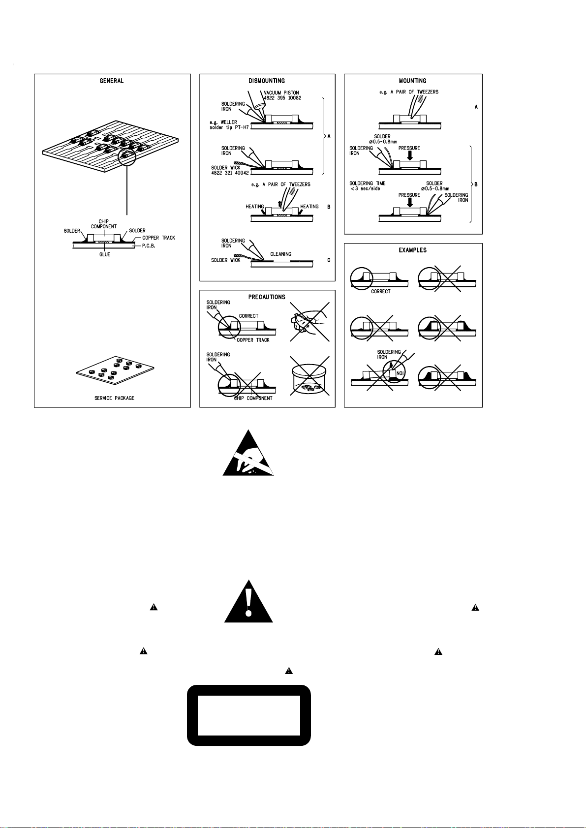
© WARNING
All ICs and many other semiconductors are susceptible to
electrostatic discharges (ESD). Careless handling during
repair can reduce life drastically.
When repairing, make sure that you are connected with the
same potential as the mass of the set via a wristband with
resistance. Keep components and tools at this potential.
f ATTENTION
Tous les IC et beaucoup d´autres semi-conducteurs sont
sensibles aux décharges statiques (ESD). Leur longévite
pourrait être considérablement écourtée par le fait qu´aucune
précaution nést prise à leur manipulation.
Lors de réparations, s´assurer de bien être relié au même
potentiel que la masse de l´appareil et enfileer le bracelet
serti d´une résistance de sécurité.
Veiller à ce que les composants ainsi que les outils que l´on
utilise soient également à ce potentiel.
d WARNUNG
Alle ICs und viele andere Halbleiter sind empfindlich
gegenüber elektrostatischen Entladungen (ESD).
Unsorgfältige Behandlung im Reparaturfall kann die
Lebensdauer drastisch reduzieren.
Sorgen Sie dafür, daß Sie im Reparaturfall über ein Pulsarmband mit Widerstand mit dem Massepotential des
Gerätes verbunden sind.
Halten Sie Bauteile und Hilfsmittel ebenfalls auf diesem
Potential.
ñ WAARSCHUWING
Alle IC´s en vele andere halfgeleiders zijn gevoelig voor
electrostatische ontladingen (ESD).
Onzorgvuldig behandelen tijdens reparatie kan de levensduur
drastisch doen vermindern. Zorg ervoor dat u tijdens reparatie
via een polsband met weerstand verbonden bent met hetzelfde
potentiaal als de massa van het apparaat.
Houd componenten en hulpmiddelen ook op ditzelfde potentiaal.
i AVVERTIMENTO
Tutti IC e parecchi semi-conduttori sono sensibili alle scariche
statiche (ESD).
La loro longevità potrebbe essere fortemente ridatta in caso di
non osservazione della più grande cauzione alla loro
manipolazione. Durante le riparationi occorre quindi essere
collegato allo stesso potenziale che quello della massa
delápparecchio tramite un braccialetto a resistenza.
Assicurarsi che i componenti e anche gli utensili con quali si
lavora siano anche a questo potenziale.
©
Safety regulations require that the set be restored to its
original condition and that parts which are identical with
those specified be used.
Safety components are marked by the symbol
i
Le norme di sicurezza estigono che l´apparecchio venga
rimesso nelle condizioni originali e che siano utilizzati i
pezzi di ricambiago identici a quelli specificati.
Componenty di sicurezza sono marcati con
ñ
Veiligheidsbepalingen vereisen, dat het apparaat in zijn
oorspronkeliijke toestand wordt teruggebracht en dat
onderdelen, identiek aan de gespecificeerde, worden toegepast.
De Veiligheidsonderdelen zijn aangeduid met het symbool
s Varning !
Osynlig laserstrålning när apparaten är öppnad och
spärren är urkopplad. Betrakta ej strålen.
∂ Advarsel !
Usynlig laserstråling ved åbning når sikkerhedsafbrydere
er ude af funktion. Undgå udsaettelse for stråling.
ß Varoitus !
Avatussa laitteessa ja suojalukituksen ohitettaessa olet alttiina
näkymättömälle laserisäteilylle. Älä katso säteeseen !
f
"Pour votre sécurite, ces documents doivent être utilisés par
des spécialistes agréés, seuls habilités à réparer votre
appareil en panne".
ESD
SAFETY
d
Bei jeder Reparatur sind die geltenden Sicherheitsvorschriften zu beachten. Der Originalzustand des Gerätes
darf nicht verändert werden. Für Reparaturen sind Originalersatzteile zu verwenden.
Sicherheitsbauteile sind durch das Symbol markiert.
f
Les normes de sécurité exigent que l`appareil soit remis
à l`état d`origine et que soient utilisées les pièces de
rechange identiques à celles spécifiées.
Les composants de sécurité sont marqués
CLASS 1
LASER PRODUCT
©
DANGER: Invisible laser radiation when open.
©
After servicing and before returning the set to customer
perform a leakage current measurement test from all
exposed metal parts to earth ground, to assure no
shock hazard exists.
The leakage current must not exceed 0.5mA.
AVOID DIRECT EXPOSURE TO BEAM.
HANDLING CHIP COMPONENTS
Page 3

2 - 1
SERVICE TOOLS
TORX T10 screwdriver with shaftlength 150mm.........................................4822 395 50423
TORX screwdriver set SBC 163...............................................................4822 295 50145
Audio signal disc SBC 429........
..............................................................4822 397 30184
Playability test disc SBC 444...................................................................4822 397 30245
Test disc 5 (disc without errors ) +
Test disc 5A (disc with dropout errors, black spots and fingerprints)
SBC 426/426A.....................................................................4822 397 30096
Burn in test disc (65 min. 1kHz signal at -30 dB level without “pause”)
.....4822 397 30155
Universal test cassette Fe SBC 420
........................................................4822 397 30071
anti-static table mat large 1200x650x1.25mm 4822 466 10953
small 600x650x1.25mm 4822 466 10958
anti-static wristband 4822 395 10223
connection box (3 press stud connections, 1MΩ)
4822 320 11307
4822 320 11305
extendible cable (2m, 2MΩ, to connect wristband to connection box)
connecting cable (3m, 2MΩ, to connect table mat to connection box) 4822 320 11306
earth cable (1MΩ, to connect any product to mat or to connection box) 4822 320 11308
KIT ESD3 (combining all 6 prior products - small table mat) 4822 310 10671
wristband tester 4822 344 13999
AVAILABLE ESD PROTECTION EQUIPMENT
TECHNICAL SPECIFICATIONS
GENERAL
Mains voltage -/21
-/22/25
: 110 - 127 / 220 - 240V
230V ± 10%
Mains frequency
-/22/25
: 50 / 60 Hz Switchable
50 Hz
Battery
remote
:3 V (R6 x 2)
Power consumption
normal :
Standby
:< 3 W
Dimension (W x H x D)
: 156 x 222 x 216 mm
Weight (without speakers)
: 2.95 Kg
AMPLIFIER
Output power mains : 2 x 5 W RMS
Speaker impedance
:2 x 3 ohm
Frequency response within ±3dB
: 60 Hz - 14 kHz
TUNER - FM SECTION
: 87.5 - 108 MHz
IF frequency
: 10.7 MHz ± 0.02 MHz
Sensitivity
:
< 22 dBf at 26dB S/N
Selectivity
300kHz : 40 dB
IF rejection
: 65 dB
Image rejection
:> 20 dB
Distortion at RF1mV, Dev. 75kHz
:< 3%
TUNER - AM SECTION
Tuning range MW 531 - 1602 kHz
IF frequency
450 kHz ± 1 kHz
Sensitivity
:
≥ 18 dB S9 / 300kHz
IF rejection
:> 24 dB
Distortion at RF=50mV, M=80%
:< 5%
Image rejection ratio
:> 20 dB
AUDIO CASSETTE RECORDER
Frequency response : 80 - 10000 Hz (8dB)
Wow & flutter : ≤ 0.48 % JIS
Tape speed : 4.76 cm/s ± 3 %
Fast wind/Rewind C60 :
< 130 s
S/N ratio (unw.) Ferro : 36 dB
DISC PLAYER
Frequency response : 63Hz - 14kHz < ±3dB
S/N ratio (A-wght.) : > 62 dBA
Total harmonic distortion : < 1.5 %
Channel separation 1 kHz : 35 dB
Channel unbalance : < ± 2 dB
Clock accuracy
:
15 W
< 4 seconds per day
Dynamic Bass Boost
: DBB1, DBB2, Off
Headphone output at 32Ω : 15mW ± 2dB (Max Vol.)
Grid
Grid -/22/25: 9kHz
-3 dB Limiting Point
:< 23.5 µV
Crosstalk at RF1mV, Dev. 40kHz
:> 26 dB
:> 35 dB for Freq > 40kHz
: 15/50 µS
Outband attentuation
Emphasis
Bias system : 73 kHz ± 10
Channel separation 1kHz:> 18 dB
Channel difference at overall
:
≤ 4 dB
≤
Normal
:
-/21
:
-/22/25
:
:
Tuning range :
:
50kHz/100kHz
-/21
:
:
50kHz
-/22/25
530 - 1700 kHz
-/21
:
-/21: 9kHz/10kHz
:
Page 4

2 - 2
Bandpass
250Hz-15kHz
e.g. 7122 707 48001
LF Voltmeter
e.g. PM2534
DUT
RF Generator
e.g. PM5326
S/N and distortion meter
e.g. Sound Technology ST1700B
Tuner SW
To avoid atmospheric interference all AM-measurements have to be carried out in a Faraday«s cage.
Use a bandpass filter (or at least a high pass filter with 250Hz) to eliminate hum (50Hz, 100Hz).
Ri=50Ω
Aerial replacement
Capacitor
R=50Ω
Bandpass
250Hz-15kHz
e.g. 7122 707 48001
LF Voltmeter
e.g. PM2534
DUT
S/N and distortion meter
e.g. Sound Technology ST1700B
Frame aerial
e.g. 7122 707 89001
Tuner AM (MW,LW)
To avoid atmospheric interference all AM-measurements have to be carried out in a Faraday«s cage.
RF Generator
e.g. PM5326
Ri=50Ω
Low pass filter 22kHz
L
R
LEVEL METER
e.g. Sennheiser UPM550
with FF-filter
S/N and distortion meter
e.g. Sound Technology ST1700B
DUT
CD
Use Audio Signal Disc SBC429 4822 397 30184 (replaces test disc 3)
L.P.F. = 13
th
order filter 4822 395 30204
Page 5
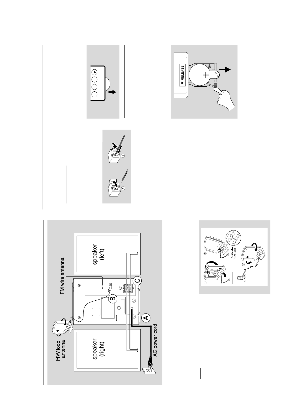
PREP ARATIONS AND CONTROLS
Preparations
Rear connections
The type plate is located at the rear of the
system.
For users in the U.K.: please follow the
instructions .
A
Power
Before connecting the AC power cord to the
wall outlet, ensure that all other connections
have been made.
WARNING!
–For optimal performance, use only the
original power cable.
–Never make or change any connections
with the power switched on.
To avoid overheating of the system
, a safety
circuit has been built in. Therefore, your
system may switch to Standby mode
automatically under extreme conditions. If
this happens, let the system cool down
before reusing it (not available for all versions).
B
Antennas Connection
Connect the supplied AM loop antenna and FM
antenna to the respective terminals. Adjust the
position of the antenna for optimal reception.
AM Antenna
● Position the antenna as far as possible from a TV,
VCR or other radiation source.
Preparations
FM Antenna
● Extend coil antenna at the back of the unit fully
for optimum reception.
C
Speakers Connection
Front Speakers
Connect the speaker wires to the SPEAKERS
terminals, right speaker to "RIGHT" and left
speaker to "LEFT", coloured (marked) wire to
"+" and black (unmarked) wire to "-".
● Fully insert the stripped por tion of the speaker
wire into the terminal as shown.
Notes:
–For optimal sound performance, use the
supplied speakers.
– Do not connect more than one speaker to any
one pair of
+
/
-
speaker terminals.
– Do not connect speakers with an impedance
lower than the speakers supplied. Please refer to
the SPECIFICATIONS section of this manual.
Before using the remote control
1
Pull out the plastic protective sheet.
2
Select the source you wish to control by
pressing one of the source select keys on the
remote control (for example CD, TUNER).
3
Then select the desired function (for example
É, í, ë).
REPEAT
SHUFFLE
SLEEP
VOL
Replacing battery (lithium
CR2025) into the remote control
1
Pull out the knob
A
slightly to the right.
2
Pull out the battery compar tment
B
.
3
Replace a new battery and fully inser t the
battery compar tment back to the original
position.
CAUTION!
Batteries contain chemical substances, s o
they should be disposed off properly.
PUSH
PULL
3-1
Page 6
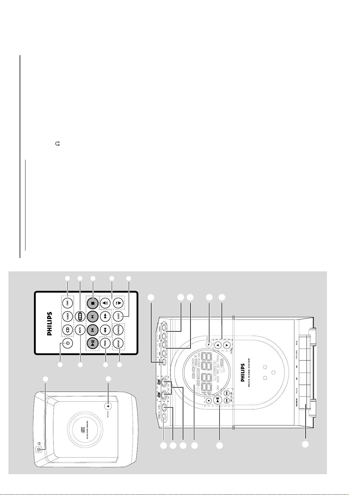
PREP ARATIONS AND CONTROLS
#
@
0
!
$
1
2
3
5
7
%
1
2
6
3
4
5
9
0
7
8
!
Controls
Controls on the system and
remote control
1
STANDBY-ON / y
–switches the system to standby/on.
2
SOURCE (CD/ TUNER/ TAPE)
–switches on the system.
– selects the respective sound source for CD/ FM/
MW/ TAPE.
3
DBB1 / DBB2 (DBB)
–(Dynamic Bass Boost) enhances the bass.
4
Display
– shows the status of the system.
5
Mode Selection
STOP 9
for CD ................. stops CD playback or erase a
CD program.
PLAY•PAUSE ÉÅ
for CD ................. starts or pauses CD playback.
¡1 / 2™ / à TUNE á (í /ë)
for CD ................. skips to the beginning of a
current track/previous/ next
track.
fast searches back and forward
within a track/CD.
for Tuner ............. tunes to radio stations.
................................. selects a preset radio station.
6
Ta pe Deck Operation
RECORD 0 ....... starts recording.
PLAY 2 ................. starts playback.
à / á ............... fast rewinds/forwards the tape.
STOP•OPEN ... stops the tape; opens the tape
compartment.
PA US E ................... pauses recording or playback.
7
VOLUME 3 / 4 (VOL 3 / 4 )
– adjusts volume level.
– adjusts the hours and minutes for clock/ timer
functions.
8
iR SENSOR
– infrared sensor for remote control.
9
TIMER / CLOCK
– activates/deactivates or sets the timer function.
– sets the clock function.
–views the clock time.
0
REPEAT / SHUFFLE
– repeats a track/CD program/ entire CD.
–plays CD tracks in random order.
!
PROGRAM (PROG)
for CD .................programs tracks and reviews the
program.
for Tuner ............. programs tuner stations manually
or automatically.
@
– connect headphones.
#
OPEN•CLOSE
– opens/closes the CD door.
$
MUTE
–switches playback sound off and on.
%
SLEEP
– activates/deactivates or selects the sleeper time.
Notes for remote control:
– First select the source you wish to control
by pressing one of the source select keys on
the remote control (for example CD ,
TUNER).
– Then select the desired function (for
example
É
,
í
,
ë
).
3-2
Page 7

PREP ARATIONS AND CONTROLS
Important notes for users in the
U.K.
Mains plug
This apparatus is fitted with an approved 13
Amp plug. To change a fuse in this type of plug
proceed as follows:
1
Remove fuse cover and fuse.
2
Fix new fuse which should be a BS1362 5 Amp,
A.S.T.A. or BSI approved type.
3
Refit the fuse cover.
If the fitted plug is not suitable for your socket
outlets, it should be cut off and an appropriate
plug fitted in its place.
If the mains plug contains a fuse, this should
have a value of 5 Amp. If a plug without a fuse
is used, the fuse at the distribution board
should not be greater than 5 Amp.
Note: The severed plug must be disposed of to
avoid a possible shock hazard should it be
inserted into a 13 Amp socket elsewhere.
How to connect a plug
The wires in the mains lead are coloured with
the following code: blue = neutral (N),
brown = live (L).
¶ As these colours may not correspond with the
colour markings identifying the terminals in
your plug, proceed as follows:
–Connect the blue wire to the terminal
marked N or coloured black.
–Connect the brown wire to the terminal
marked L or coloured red.
–Do not connect either wire to the ear th
terminal in the plug, marked E (or e) or
coloured green (or green and yellow).
Before replacing the plug cover, make cer tain
that the cord grip is clamped over the sheath
of the lead - not simply over the two wires.
Copyright in the U.K.
Recording and playback of material may
require consent. See Copyright Act 1956 and
The Performer’s Protection Acts 1958 to 1972.
Norge
Typeskilt finnes på apparatens underside.
Observer: Nettbryteren er sekundert
innkoplet. Den innebygde netdelen er
derfor ikke frakoplet nettet så lenge
apparatet er tilsluttet nettkontakten.
For å redusere faren for brann eller elektrisk
støt, skal apparatet ikke utsettes for regn eller
fuktighet.
Italia
DICHIARAZIONE DI CONFORMITA ’
Si dichiara che l’apparecchio MC230, MC235
Philips risponde alle prescrizioni dell’ar t. 2
comma 1 del D.M. 28 Agosto 1995 n. 548.
Fatto a Eindhoven
Philips Consumer Electronics
Philips, Glaslaan 2
5616 JB Eindhoven, The Netherlands
CAUTION
Use of controls or adjustments or
performance of procedures other than
herein may result in hazardous
radiation exposure or other unsafe
operation.
VAROITUS
Muiden kuin tässä esitettyjen
toimintojen säädön tai asetusten
muutto saattaa altistaa vaaralliselle
säteilylle tai muille vaarallisille
toiminnoille.
3-3
Page 8

PREP ARATIONS AND CONTROLS
Troubleshooting
WARNING
Under no circumstances should you try to repair the system yourself, as this will invalidate the
warranty. Do not open the system as there is a risk of electric shock.
If a fault occurs, first check the points listed below before taking the system for repair. If you
are unable to remedy a problem by following these hints, consult your dealer or service centre.
Problem Solution
CD OPERATION
“no cd” is displayed. –Insert a disc.
– Check if the disc is inserted upside down.
–Wait until the moisture condensation at the lens
has cleared.
– Replace or clean the disc, see “Maintenance”.
– Use a finalised CD-RW or CD-R.
RADIO RECEPTION
Radio reception is poor. – If the signal is too weak, adjust the antenna or
connect an external antenna for better reception.
–Increase the distance between the Micro HiFi
System and your TV or VCR.
TAPE OPERATION / RECORDING
Recording or playback cannot be made. –Clean deck parts, see “Maintenance”.
– Use only normal (IEC I) tape for recording.
– Apply a piece of adhesive tape over the missing
tab space.
GENERAL
The system does not react when buttons – Remove and reconnect the AC power plug and
are pressed. switch on the system again.
Sound cannot be heard or is of poor – Adjust the volume.
quality. –Disconnect the headphones.
– Check that the speakers are connected correctly.
– Check if the stripped speaker wire is clamped.
The left and right sound outputs are – Check the speaker connections and location.
reversed.
The remote control does not function – Select the source (CD or TUNER, for example)
properly. before pressing the function button (É,í,ë).
– Reduce the distance between the remote control
and the system.
–Insert the batteries with their polarities
(+/– signs) aligned as indicated.
–Replace the batteries.
–Point the remote control directly toward
IR sensor on the front of the system.
The timer is not working. – Set the clock correctly.
– Press TIMER to switch on the timer.
– If a recording is in progress, stop the recording.
The Clock/Timer setting is erased. –Power has been interrupted or the power cord
has been disconnected. Reset the clock/timer.
Tr oubleshooting
3-4
Page 9

DISASSEMBLY DIAGRAM
A. To remove Rear Cabinet
B. To remove CD Tray
C. To remove Main Board
D. To remove CD Board
E. To remove Tape Deck
F. To remove LCD Board
G. To remove Cassette Key Plate
H. To remove Transformer Holder
4-1
4-1
2
2
2
2
4
5
2
2
2
3
5
3
4
3
4
Page 10

4-2
Abbreviations and Pin-description of ICs
SERVO PROCESSOR SAA7379HL
4-2
SYMBOL PIN I/O DESCRIPTION
LFPOWER1 I laser power supply
EXFILTER 2 O 10 nF capacitor for laser start-up control
MONITOR3 I laser monitor diode
SENSE4 I OPU ground reference point for MONITOR measurement
V
I
V
V
REF
SSA1
DDA1
REFO
5SUP analog ground1
6Oreference current output (24k Ω resistor connected to analog ground)
7SUP analog supply voltage1
8I/O servo reference voltage
D1 9 I diode voltage/current input (central diode signal input)
D2 10 I diode voltage/current input (central diode signal input)
D3 11 I diode voltage/current input (central diode signal input)
D4 12 I diode voltage/current input (central diode signal input)
R1 13 I diode voltage/current input (satellite diode signal input)
R2 14 I diode voltage/current input (satellite diode signal input)
CSLICE 15 I/O 10n F capacitor for adaptive HF data slicer
V
V
DDA2
SSA2
16 SUP analog supply voltage2
17 SUP analog ground 2
OSCOUT 18 O crystal/resonator output
OSCIN1 9 I crystal/resonator input
V
SSA3
20 SUP analog ground 3
DACGND 21 I audio DAC ground
DACRP2 2 O audio DAC right channel differential positive output
DACRN2 3 O audio DAC right channel differential negative output
DACV
ref
DACLN2 5 O audio DAC left channel differential
DACLP2 6 O audio DAC left channel differential
DACV
pos
BUFV
pos
24 I/O audio DAC decoupling point (10 µF or 100 nF to ground
negative output
positive output
27 I audio DAC positive supply voltage
28 I audio buffer positive supply voltage
BUFINR 29 I audio buffer right input
BUFOUTR3 0 O audio buffer right output
BUFOUTL3 1 O audio buffer left output
BUFINL 32 I audio buffer left input
BUFGND 33 I audio buffer ground
LKILL3 4 O KILL output for left channel (con
RKILL3 5 O KILL output for right channel (con
urable as open-drain)
urable as open-drain)
N/C3 6 O No connection
N/C3 7 O No connection
N/C3 8 I No connection
CFLAG3 9 O c orrection
V
SSD1
40 SUP digital ground1
g output (open-drain)
SYMBOL PIN I/O DESCRIPTION
V
DDD1
41 SUP digital supply voltage1
SDI 42 I serial data input (loopback)
WCLI 43 I word clock input (loopback)
SCLI 44 I se rial bit clock input (loopback)
EF 45 O C2 error
g output
DATA 46 O serial data output
WCLK 47 O word clock output
SCLK 48 O serial clock output
CLK16 49 O 16 MHz clock output
CLK4/12 50 O co
gurable 4M Hz or 12 MHz clock output
RESET 51 I power-on reset input (active LOW)
SDA 52 I/O microcontroller interface data input/output (open-drain)
SCL 53 I microcontroller interface clock input
RAB 54 I microcontroller interface R/W and load control input (4-wire)
SILD 55 I microcontroller interface R/W and load control input (4-wire)
STATUS 56 O servo interrupt request line/decoder status register/DC offset value
readback output
RCK 57 I subcode clock input
SUB 58 O P to W subcode output
SFSY 59 O subcode frame sync output
SBSY 60 O s ubcode block sync output
V
SSD2
61 SUP digital ground2
DOBM 62 O b i-phase mark output (externally buffered)
V
DDD2
63 SUP digital supply voltage2
RA 64 O r adial actuator output
FO 65 O focus actuator output
SL 66 O sledge actuator output
MOTO1 67 O motor output 1 output
MOTO2 68 O motor output 2 output
V
V
SSD3
DDD3
69 SUP digital ground3
70 SUP digital supply voltage3
V1 71 I versatile pin 1 input
V2 72 I versatile pin 2 input
V3 73 O versatile pin 3 output
V4 74 O versatile pin 4 output
V5 75 O versatile pin 5 output
TEST1 76 I test pin 1 input
TEST2 77 I test pin 2 input
TEST3 78 I test pin 3 input
TEST4 79 I test pin 4 input
LASER 80 O laser drive output
Page 11

4-3 4-3
BLOCK DIAGRAM OF INTEGRATED CIRCUIT
SERVO PROCESSOR SAA7379HL
handbook, full pagewidth
V
DDA1
V
DDA2
I
REF
V
REFO
SCL
SDA
RAB
SILD
TEST1
TEST2
TEST3
TEST4
OSCIN
OSCOUT
CLK16
CLK4/12
CDTRDY
CDTDAT A
CDTCLK
SFSY
SUB
RCK
SBSY
STAT US
RESET
D2 D3 D4 R1 R2
D1
10 11 12 13 14 34 21
9
DC OFFSET COMPENSAT ION
7
16
6
8
53
52
54
55
76
77
78
79
19
18
49
50
36
37
38
59
58
57
60
56
51
V
VOL TAGE
BUFFER
HF AND LF CAPTURE
BIAS
GENERATOR
CONTROL
PA R T
MICROCONTROLLER
INTERFACE
TEST
TIMING
CD TEXT
INTERFACE
INTERFACE
CONTROL
DECODER
MICRO-
CONTROLLER
INTERFACE
40 71 72 73 74 75 34 35 33 28
SSD1
V
SSD2
61
V
SSD3
69
V
41
63
V
DDD2
DDD1VDDD3
V
SSA2
V
V
SSA1
5
17
D1 TO D4
SUM
HIGH-PASS FILTER
DATA SLICER AND
THRESHOLD
CONTROL
DIGITA L
PLL
EFM
DEMODULAT OR
SRAM
RAM
ADDRESSER
SUBCODE
PROCESSOR
SAA7379
SAA7824
VERSAT ILE PINS
INTERFACE
70
V2
V1
V3 V4 V5 LKILL RKILL
SSA3
20
MONITOR
SENSE
MONITOR
ADC
CONTROL FUNCTION
ANTI ALIAS
DISC ADC
PEAK
DETECT
CONTROL LOGIC
PROCESSOR
EXFILTER
LASER POWER
AUDIO
KILL
LPOWER
LASER
OUTPUT
STAGES
MOTOR
CONTROL
ERROR
CORRECTOR
FLAGS
EBU
INTERFACE
SERIAL
DATA
TERFACE
IN
SERIAL
DATA
(LOOPBACK
INTERFACE
DEM
DAC
HEADPHONE
BUFFERS
BUFV
BUFGND
)
pos
80
64
65
66
15
67
68
39
62
45
48
47
46
44
43
42
27
22
23
26
25
24
21
29
32
30
31
LAS
RA
FO
SL
CSLICE
MOTO1
MOTO2
CFLAG
DOBM
EF
SCLK
WCLK
DATA
SCLI
WCLI
SDI
DAC V
DAC RP
DAC RN
DACLP
DACLN
DAC V
DACGND
BUFINR
BUFINL
BUFOUTR
BUFOUTL
MBL436
ER
pos
ref
BLOCK DIAGRAM OF INTEGRATED CIRCUIT
SELF TUNED RADIO TEA5757
.This text is here in
orce landscape pages to be rotated correctly when browsing through the pdf in the Acrobat reader.This text is here inThis text is here in
rce landscape pages to be rotated correctly when browsing through the pdf in the Acrobat reader. white to force landscape pages to be ...
FM-IFI1 FM-IFI2
FM-MIXER
FM
MIXER
FM
AM
AM
MIXER
40 41
AM-MIXERAMOSC
AM-IFI1
FM
IF1
STATUS
REGISTER
SEQUENTIAL
CIRCUIT
AM
IF
36 44
AM-IFI/O2
FM-IFO1
AGC
AGC
up
down
level
FM
IF2
AM/FM
INDICATOR
IN-LOCK
DETECTOR
CHARGE
PUMP
hard mute
DETECTOR
IFGND FSIFMDEM
FM
DETECTOR
AFC
AM
TUNE
181739 37 333535
822
V
CC2
21
10
AFO
19 kHz
38 kHz
level
TEA5757;
TEA5759
PILOT
DETECTOR
PLL
DECODER
stereo
MATRIX
stereo
mono
SDS
MUTE
V/I
CONVERTER
11
MPXI
4
RFGND
16
PILFIL
24
MO/ST
12
LFI
9
VCO
14
AFLO
AFRO
15
13
MUTE
19
AFC
AFC
AFC
MHA111
(n)
(p)
20
32
FM-RFI
RFGND
DATA
S-CLOCK
E-ENABLE
V
STAB(A)
V
STAB(B)
V
CC1
V
DDD
RIPPLE
XTAL
DGND
AM-RFI
43
42
FM-RFO
FM
FRONT-END
FMOSC
FM
OSCILLATOR
28
27
29
38
34
7
STABILIZER
23
1
PRESCALER
MULTIPLEXER
25
CRYSTAL
26
OSCILLATOR
31
P1
30
P0
AM
2
FRONT-END
SHIFT REGISTER
LAST-STATION
PROGRAMMABLE
AM
OSCILLATOR
MEMORY
COUNTER
WINDOW
DETECTOR
6
Page 12

4-4
PIN DESCRIPTION
Pin
No.
Symbol I/O Description
Pin
No.
Symbol I/O Description
1 DO1.1 O Drive output 15 OPIN(-) I Op-amp input(-)
2 DO1.2 O Drive output 16 OPIN(+) I Op-amp input(+)
3 DI1.1 I Drive input 17 DO3.1 O Drive output
4 DI1.2 I Drive input 18 DO3.2 O Drive output
5REG - Regulator 19 DI3.1 I Drive input
6 REO O Regulator output 20 DI3.2 I Drive input
7 MUTE I Mute 21 Vcc1 Supply voltage
8 GND1 - Ground 1 22 Vcc2 Supply voltage
9 DI2.1 I Drive input 23 V
REF
I 2.5V bias voltage
10 DI2.2 I Drive input 24 DI4.1 I Drive input
11 DO2.1 O Drive output 25 DI4.2 I Drive input
12 DO2.2 O Drive output 26 DO4.1 O Drive output
13 GND2 - Ground 2 27 DO4.2 O Drive output
14 OPOUT O Op-amp output 28 GND3 Ground 3
4-4
Abbreviations and Pin-description of ICs
SELF TUNED RADIO TEA5757
PINNING
SYMBOL PIN DESCRIPTION
RIPPLE 1 ripple capacitor input
AM-RFI 2 AMRF input
FM-RFO 3 parallel tuned FMRF circuit to ground
RFGND 4 RF ground and substrate
FMOSC 5 parallel tuned FM-oscillator circuit to ground
AMOSC 6 parallel tuned AM-oscillator circuit to ground
V
CC1
TUNE 8 tuning current output
VCO 9 voltage controlled oscillator input
AFO 10 AM/FM AF output (output impedance typical 5 kΩ)
MPXI 11 stereo decoder input (input impedance typical 150 kΩ)
LFI 12 loop-filter input
MUTE 13 mute input
AFLO 14 left channel output (output impedance typical 4.3 kΩ)
AFRO 15 right channel output (output impedance typical 4.3 kΩ)
PILFIL 16 pilot detector filter input
IFGND 17 ground of IF, detector and MPX stage
FMDEM 18 ceramic discriminator input
AFC
(n)
AFC
(p)
FSI 21 field-strength indicator
V
CC2
V
DDD
MO/ST 24 mono/stereo and tuning indication output
XTAL 25 crystal input
DGND 26 digital ground
BUS-CLOCK 27 bus-clock input
DATA 28 bus data input/output
WRITE-ENABLE 29 bus write-enable input
P0 30 programmable output port (P0)
P1 31 programmable output port (P1)
AFC 32 450 kHz LC-circuit
FM-IFI2 33 FMIF input 2 (input impedance typical 330 Ω)
V
STAB(B)
FM-IFO1 35 FMIF output 1 (output impedance typical 330 Ω)
AM-IFI/O2 36 input/output to IF-Tank (IFT); output: current source
FM-IFI1 37 FMIF input 1 (input impedance typical 330 Ω)
V
STAB(A)
FM-MIXER 39 ceramic filter output (output impedance typical 330 Ω)
AM-MIXER 40 open-collector output to IFT
7 supply voltage
19 AFC negative output
20 AFC positive output
22 supply voltage for tuning
23 digital supply voltage
34 internal stabilized supply voltage (B)
38 internal stabilized supply voltage (A)
Abbreviations and Pin-description of ICs
4-CH MOTOR DRIVER D9258
BLOCK DIAGRAM AND PIN CONFIGURATION
Page 13

SET BLOCK DIAGRAM
5-1 5-1
Page 14

SET WIRING DIAGRAM
5-2 5-2
Page 15

6-1 6-1
CIRCUIT DIAGRAM - LCD, HP, KEY RECTIFIER BOARD
Page 16

6-2
6-2
LAYOUT DIAGRAM - LCD BOARD
COMPONENT LAYOUT
LAYOUT DIAGRAM - HEADPHONE BOARD
COMPONENT LAYOUT
SMD LAYOUT
SMD LAYOUT
LAYOUT DIAGRAM - KEY BOARD
COMPONENT LAYOUT
SMD LAYOUT
Page 17

LAYOUT DIAGRAM - POWER BOARD
COMPONENT LAYOUT
6-3
6-3
SMD LAYOUT
Page 18

CIRCUIT DIAGRAM - CD BOARD
7-1
7-1
Page 19

7-2 7-2
LAYOUT DIAGRAM - CD BOARD
COMPONENT LAYOUT
LAYOUT DIAGRAM - CD BOARD
SMD LAYOUT
Page 20

CIRCUIT DIAGRAM - MAIN BOARD
8-1 8-1
Page 21

CIRCUIT DIAGRAM - MAIN BOARD TUNER PART
8-2 8-2
Page 22

8-3 8-3
LAYOUT DIAGRAM - MAIN BOARD
COMPONENT LAYOUT
LAYOUT DIAGRAM - MAIN BOARD
SMD LAYOUT
Page 23

SET EXPLODED VIEW DIAGRAM
9-1
9-1
21
19
SCREW LIST
22
ITEM
DESCRIPTION
QUANTITY
23
28
18
24
4
17
24
26
12
26
9
8
11
29
22
7
16
6
27
14
13 -1
13 -6
Page 24

T
T
9-1 9-1
MECHANICAL & ACCESSORIES PARTSLIS
1 9940 000 00398 COSMETIC PANEL
2 9940 000 00397 LENS
3 9940 000 00396 LCD CHAMFER
4 9940 000 00395 KEYSET TOP
6 9940 000 00403 CASSETTE PANEL
7 9940 000 00402 CASSETTE DOOR
8 9940 000 00391 FRONT CABINET
9 9940 000 00399 KNOB PLAY
11 9940 000 00401 KNOB VOLUME
12 9940 000 00566 LCD PC BOARD ASSEMBLY
13-1 9940 000 00404 CASSETTE KEY RECORD
13-2 9940 000 00405 CASSETTE KEY PLAY
13-3 9940 000 00406 CASSETTE KEY REVERSE
13-4 9940 000 00407 CASSETTE KEY FORWARD
13-5 9940 000 00408 CASSETTE KEY STOP/OPEN
13-6 9940 000 00409 CASSETTE KEY PAUSE
14 9940 000 00387 CASSETTE DECK
16 9940 000 00383 POWER TRANSFO.230V /22/25
16 9940 000 00571 POWER TRANSFO.120/230V /21
17 9940 000 00381 CD MECHANISM DA11B3N
!
!
9940 000 00373 FFC CABLE 16P P1.0 L70
!
9940 000 00382 AC CORD VDE 230V /21/22
!
9940 000 00512 AC CORD BS PLUG 2M /25
9940 000 00507 SPEAKER BOX 5W MC150
9940 000 00508 REMOTE CONTROL
9940 000 00509 AM LOOP ANT
!
9940 000 00573 MAINS PLUG ADAPTOR /21
ELECTRICAL PARTSLIS
1707 9940 000 00389 REC SWITCH 18PIN
7705 9940 000 00388 IC, D7312CP PREAMPLIFIER
D407 9940 000 00376 CH-VARIABLE CAP DIODE, BB804
D408 9940 000 00376 CH-VARIABLE CAP DIODE, BB804
F701 9940 000 00384 FUSE PTU 1A 250V
F702 9940 000 00385 FUSE PTU 2A 250V
HP800 9940 000 00386 HP JACK MSJ-2000
IRM301 9940 000 00569 IR SENSOR 902V5A
LCD301 9940 000 00575 LCD 80356TT-P 20PIN
LED4 9940 000 00567 LED 23B53SCC29
LED5 9940 000 00567 LED 23B53SCC29
S300 9940 000 00568 TACT SWITCH
S301 9940 000 00568 TACT SWITCH
S302 9940 000 00568 TACT SWITCH
S303 9940 000 00568 TACT SWITCH
S304 9940 000 00568 TACT SWITCH
S305 9940 000 00568 TACT SWITCH
S306 9940 000 00568 TACT SWITCH
S307 9940 000 00568 TACT SWITCH
S308 9940 000 00568 TACT SWITCH
!
!
18 9940 000 00392 REAR CABINET /22/25
18 9940 000 00574 REAR CABINET /21
19 9940 000 00502 CD DOOR SPRING
21 9940 000 00393 CD DOOR
22 9940 000 00501 DAMPER GEAR ASSEMBLY
23 9940 000 00394 CD TRAY
24 9940 000 00505 CD DAMPER 658 TA 30
26 9940 000 00506 CD DAMPER 658 TB 40
27 9940 000 00503 CASSETTE DOOR SPRING
28 9940 000 00379 CD DOOR SW DLS-02-W-1
29 9940 000 00618 TAPE PCB ASS'Y
9940 000 00504 RECORD ARM
9940 000 00572 SLIDE SWITCH 1P2T /21
S309 9940 000 00568 TACT SWITCH
S310 9940 000 00568 TACT SWITCH
S311 9940 000 00568 TACT SWITCH
S312 9940 000 00568 TACT SWITCH
S314 9940 000 00568 TACT SWITCH
S315 9940 000 00568 TACT SWITCH
SP-JK 9940 000 00511 SP TERMINAL MSP-134V-05
U100 9940 000 00369 IC,L7806CV REGULATOR
U101 9965 000 12283 IC:MEMORY BR24C04F-W
U102 9940 000 00372 IC P87C54X2BDH
U4 9940 000 00564 IC SAA7379HL
U401 9351 740 80557 IC SM TEA5757H/V1 (PHSE) Y
U402 9940 000 00375 CH-VARIABLE CAP DIODE
U601 9940 000 00374 IC,BA4558F OPERATIONAL
U9 9940 000 00565 IC D9258 MOTOR DRIVER
VC402 9940 000 00378 TRIMMER CAP 220VDC +50%-0%
VC403 9940 000 00378 TRIMMER CAP 220VDC +50%-0%
Note: Only these parts mentioned in the list are normal
normal service parts.
Note: Only these parts mentioned in the list are normal
normal service parts.
 Loading...