

Page 1
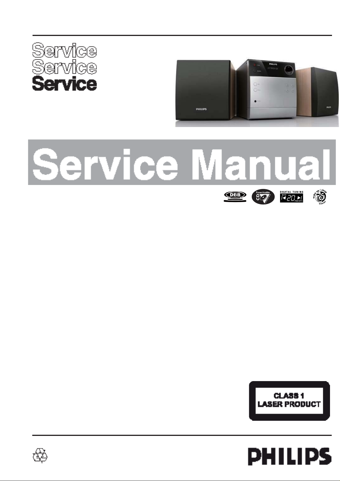
CD playback Compact design Micro Hi-Fi System
MC127
-/05/12
CONTENTS
Technical specification and disassembly diagrams..........................1
Service and safety instructions.........................................................2
Block diagram ................................................................................3-1
Wiring diagram ..............................................................................4-1
DISPLAY+ MAIN+ TUNER+ LINE IN board
Circuit diagram...................................................................5-1..5-3
Layout diagram .........................................................................5-4
Power board
Circuit diagram .........................................................................6-1
Layout diagram .........................................................................6-2
Exploded view diagram .................................................................7-1
Revision list ...................................................................................8-1
©
Copyright 2011 Philips Consumer Electronics B.V. Eindhoven, The Netherlands
All rights reserved. No part of this publication may be reproduced, stored in a retrieval
system or transmitted, in any form or by any means, electronic, mechanical, photocopying,
or otherwise without the prior permission of Philips.
Published by SW 1125 Service Audio Subject to modification
Version 1.0
3141 785 36420
Page 2
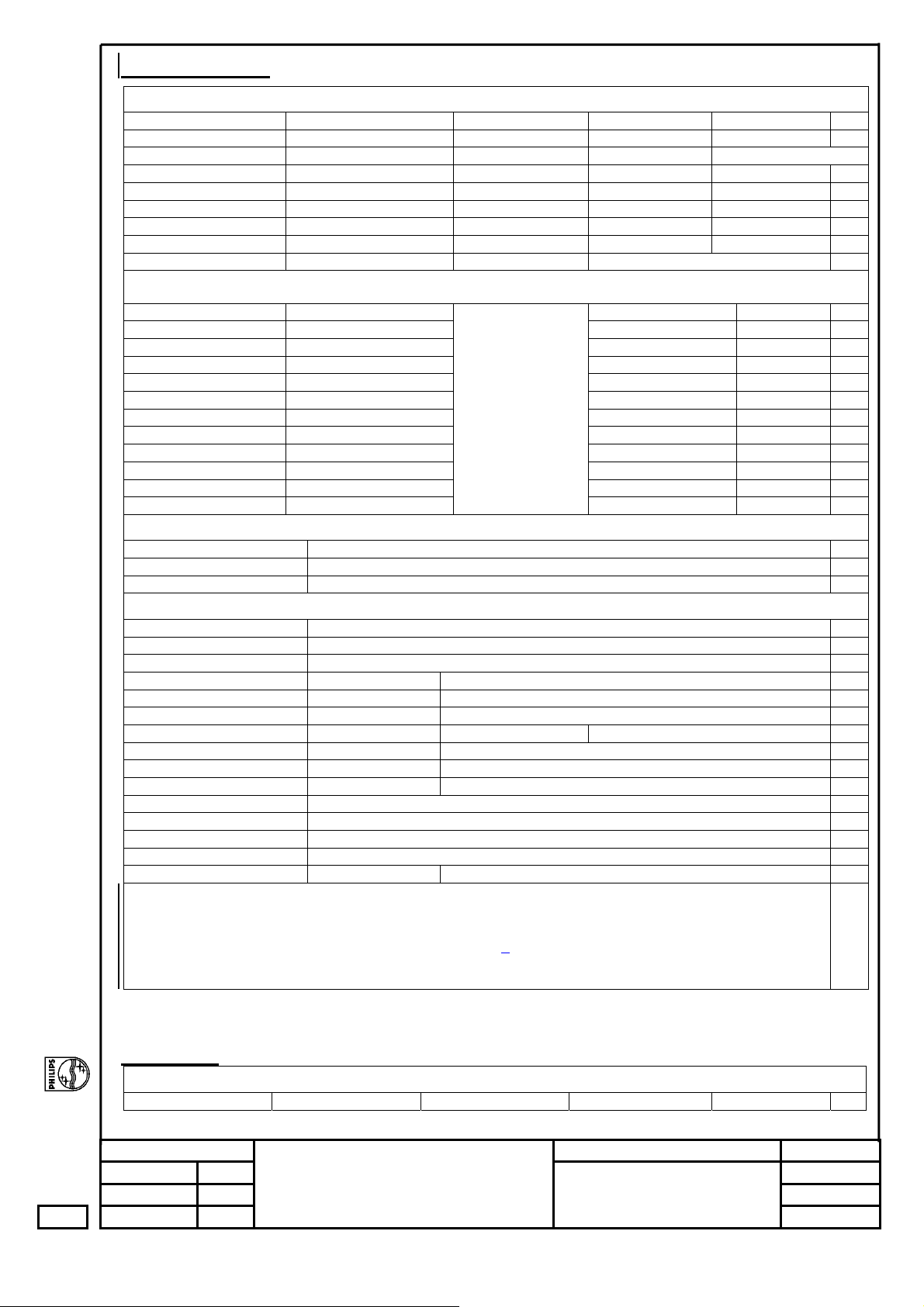
General description: MC127- PORTABLE CD SOUNDMACHINE TUNER
LIFETIME : 5 YEARS (ACC. TO UAN-D1611)
PERFORMANCE CLASSES :
TUNER
SUPPLY,
AMPLIFIER
I x x x 3
II x 4
III 5
SAFETY REQUIREMENTS:
IEC 60065:2001(SEVENTH EDITION)+AI:2005------SAFETY
RADIATION, IMMUNITY REQUIREMENTS: (EMC)
EN55013:2001+A1:2003+A2:2006;EN55020:2007 EN61000-3-2:2006+A2:2009;EN61000-3-3:2008
EN61000-4-5:2006; EN61000-4-11:2004
CLIMATIC REQUIREMENTS: (acc. to UAN-D1590)
All climates: -10 °C till +50 °C (Functional); Set has to be pre-conditioned for 2 hour, except CD function 8
For all measurements: 25 °C 9
POWER SUPPLY:
MAINS (AC) operation DC (int. or ext.) operation / Backup Buffer
Voltage
Battery type: 10
selection:
Selection:
See table below
Frequency: External DC: No 12
POWER CONSUMPTION:
Standby: Less than <1W
Maximum: 12W Maximum: 14
General:
Q and R according to production division rules : Q < 1% (Major), Q < 4% (Minor)
Measured according to: R < 3% (CE52)
DERIVED VERSIONS: APPROBATION
Versio
n
93
Voltage on
typeplate
240V, 50Hz
REMARKS:
SPEAKER
BOXES
RECORDER CLOCK CD DCC TELEPHONE
Standby: 13
Tolerance Frequency Tuner
10%
(216V – 264V);
50Hz
FM,
REC.
PLAYER
6
7
11
UK
15
16
1
2
TUNER PART
TECHNICAL description:
2011-04-01
1
2
3
CDSM WITH
MC127
SET SPECIFICATION
Page 3
(circuitry) FM (active components) FM
RF
SI4704 SI4704
1
IF
Detector
Decoder
SI4704 SI4704
SI4704
GENERAL part:
WAVE RANGE TOLERANCES TUNING
FM 87.5MHz - 0.3 MHz
108MHz + 0.5 MHz
9
10
AERIAL:
FM telescope - 540 mm 12
FM wire : N/A Execution - Rotational 180° 13
INDICATORS:
Pointer stroke: Execution pointer: 14
Knob indication over: Field Strength: 15
ELECTRICAL DATA:
AM: nom. limit FM:
wave range Sensitivity for
18 24 55 122dB
22 20 50 111dB
FM
nom.
lim.
31
μV/m
unit
REMARKS:
SUPPLY, AF-AMPLIFIER & LOUDSPEAKER (Boxes) PART:
TECHNICAL description:
2011-04-01
1
2
3
QD
noise limited sensitivity
50mW
dBμV/m
dBf
μV
CDSM WITH
MC127
-3dB limiting point
Amplification reserve
AFC holding range
Distortion (RF 1mV, Δf 67.5kHz)
Stereo -46dB quieting
Cross-talk (RF 1mV, Δf 40kHz,
1kHz)
IF
(26dB)
Image
rejectio
n
IF
rejectio
n
dBf dB dB dB
large
signal
f
f
mV/m
SET SPECIFICATION
1MHz 6
1MHz 7
nom.
20 26 dBf
0 -4 dB
-
1 7 %
48 52
25 20 dB
limit
29
30
2
3
4
5
8
16
17
18
19
20
21
22
23
24
25
26
27
28
Page 4
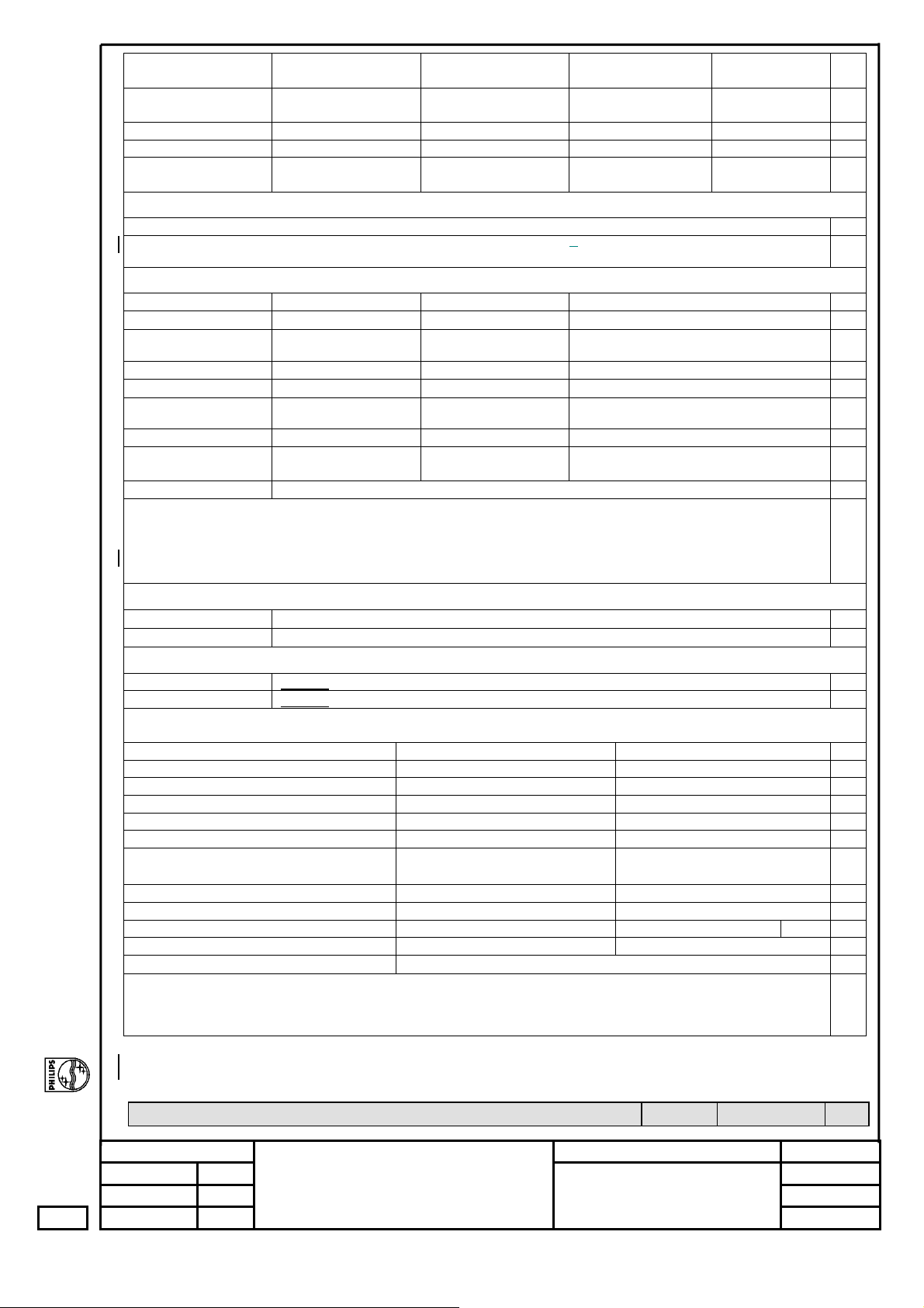
Power supply Tone Control AF-Amplifier Loudspeaker
Active
components
Passive
components
4
GENERAL part:
Aux in jack type Ø 3.5mm 5
Loudspeaker filter, high pass None 6
Loudspeaker filter, low pass None 7
Power stage protection Temperature – YES; Short circuit – YES 8
Public address No 9
INDICATORS:
Output power or VU-meter No 11
Frequency response No 12
Low power (battery) No
14
UTC8227 1
2 X 8Ω, 2W
3
13
ELECTRICAL DATA:
TONE/EQUALIZER/DBB
DSC Balance control No 15
Mechanical noise (ISO 1996) 16
Noise overall (ISO) 17
Channel difference at -46dB Type: < 3 dB 18
Hum (vol.max.-20dB to vol.min.) Limit: 2mV 19
Residual noise(volume min) Limit: 2mV 20
DBB on (Vol.max.-20dB): 100Hz, +6dB
(±2dB) w.r.t. 1kHz at DBB on
DBB off (Vol.max.-20dB): 100Hz, -2dB
(±2dB) w.r.t. 1kHz at DBB on
Input sens.:Nom. 500 mV 23
for 50mW Limit: 600 mV 24
Line outp.: Nom. mV 25
voltage Limit: mV 26
OUTPUT POWER:
Mains operation: D=10%
28
Music power (MPO) / (PMPO): (acc. to DIN45324) 29
Short term maximum output power: - (acc. to IEC 60268-15) 30
Long term maximum output power: - (acc. to IEC 60268-15) 31
Headphone output voltage/power: n.a. 32
Bandwidth FTC – 1dB at: n.a. (acc. to FTC/16/1/D/432) 33
Bandwidth DIN – 3dB at: - (acc. to IEC 60268-15) 34
Frequency response at Vol. max – 20dB:
LOUDSPEAKER (output):
Low pass crossover frequency: - kHz tolerance: Hz 36
High pass crossover frequency: - kHz tolerance: Hz 37
Short term maximum output power: - W (acc. to IEC 60268-15) 38
Long term maximum output power: - W (acc. to IEC 60268-15) 39
Frequency response at: - Hz kHz 41
REMARKS:
27 : Measured in Tuner mode;
28: CD or Tape mode.
DBB has no dynamic, fixed to
6dB
22
2 X 1W 8Ω
typ. 60Hz to 20kHz (±
3dB)
Limit: -1dB 27
35
21
42
2011-04-01
1
2
3
CDSM WITH
MC127
SET SPECIFICATION
Page 5
TAPE function: (ECO-MTF-PA-SD-MS (FE) Module)
General description:
3
5
6
7
Mechanical specification:
8
1
2
4
10
11
12
13
14
15
16
17
18
19
Indicators:
Recording level No 21
Play back level No 22
Tape counter No 23
Electrical data:
Bias system FM/AM 24
RIF switch No 25
Erase system FM/AM 26
Erasing damping 27
Channel separation (IEC1) 28
Track separation (IEC1) 29
Frequency response (PB) 30
SNR 250nWb/m 31
Signal/hiss 250nWb/m 32
Signal/hum 250nWb/m 33
Channel difference (PB) 34
Distortion 250nWb/m 35
ALC attack time 36
ALC release time 37
Crosstalk Between forward to reverse track 38
REMARKS: 31: * not according to PQR clause 18.5 class I
31: ** Chromium performance not fulfilled
Amplification Reserve for Tape = 1dB ±2dB
20
9
39
For details, please see specification SH-190 of ECO-MTF-PA-SD (3140 117 14890).
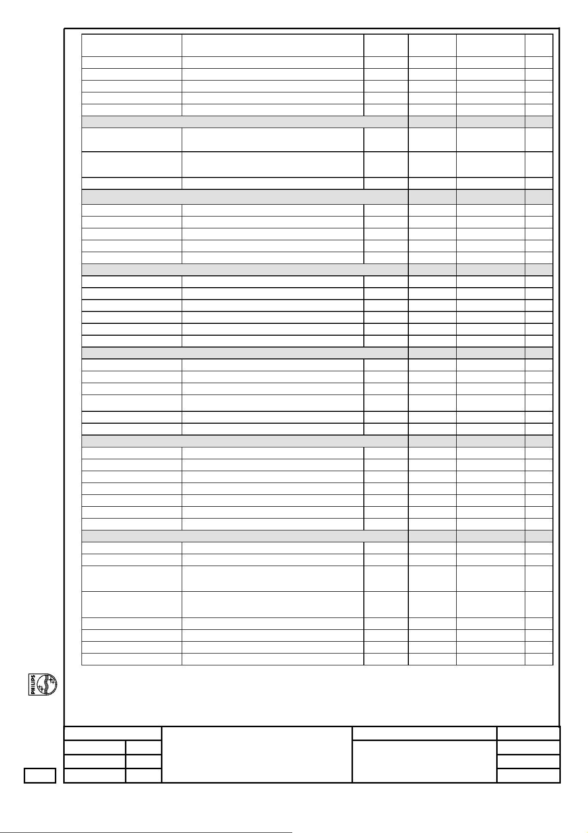
CD-PART
Technical description:
Input Output Motor/control Logic control 1
: ( CD MECHAISM-DA11B3VF)(SANYO) 5
2011-04-01
1
2
3
CDSM WITH
MC127
SET SPECIFICATION
Page 6
Active components MMSA9258(Mitsu
mi)
Passive
components
Signal processing HF-preamplifier
Active components SC9614 SC9614 SC9640 5
Passive
components
Indicators/Display/Keys:
Display: Digits LCD for Track No. display 7
Keys: one 4-position slider switch, 6 tact switches on unit, 6 for CD -: Play, Stop, Previous/Search down,
Next/Search up, Program/Program review, CD-modes (Repeat/Shuffle)
Playability: (acc. To AR 30-05-239)
Limit Typical Testdisc 9
Wedge
Eccentric
Fingerprint No audible defect TNO 11of Subchassis 8A 12
Black dot
Skew 0.6mm No audible defect TNO 1,6 of 0.6mm skew (7104 099
Bad HF track No audible defect TNO 8 of Subchassis 8A 15
Heavy fingerprint No track
Playback position Horizontal, Normal position (Set is located on a flat surface, floor) 17
- Playback of above mentioned tracks possible without track loss or audible defects. 18
- Double black dot, max. diameter, thin/thick disk is according to PQR or AR 30-05-239)
- This unit can playback (only) CD-R or CD-RW discs. For performance specification, please refer to
module
specification of CD99 (3103 308 52190)
Shock resistance: (acc. to AR 13-A6-CD-068)
± Z axis
± X or Y axis
Acoustical noise:
Mode: Play/Pause 35 dBA max. (45 dbA in Search mode) 21
Mode: Jump (Next) 45 dBA max. 22
AUDIO part: (Measured with Audio Signals Disc-1, 7104 078 04911 on Speakers or Headphone socket with nom.
load)
Typ. Limit 23
Output level (TNO1) 24
SNR unwtd. 60 dB 48 dB 25
SNR wtd. dBA 65 dBA 57 dBA 26
Crosstalk (1kHz) 40 dB 26 dB 27
Crosstalk (10kHz) 30 dB 16 dB 28
Frequency response
Vol.max.–20dB (DBB on)
THD (1kHz, -6 dB) 0.2 % 2 % 30
THD (10 kHz, -20 dB) < 1 % < 3 % 31
Channel difference 2 dB 3 dB 32
Frequency accuracy - +/-0.5 % 33
De-emphasis
REMARKS:
3
6
500 μm 700 μm
150 μm 200 μm TNO 1,24 of 200μm disc
500 μm 600 μm
TNO 10 of Subchassis 8A 16
jumps/plops
5 G 19
5 G m 20
+9dB
+3dB
15μs / 50μs Switchable via Subcode information
TNO 7,9 of SBC 444A (7104 099 24990) 10
24960)
TNO 13 of SBC 444A (7104 099 24990) 13
28260)
±2dB at 100Hz
±2dB at 10kHz
- Amplification reserve for CD = +2dB (±2dB); Ref. Level for CD is a 0dB track instead of a –6dB track.
SC9640 2
Servoprocessor
(7104 099
4
8
11
14
29
34
35
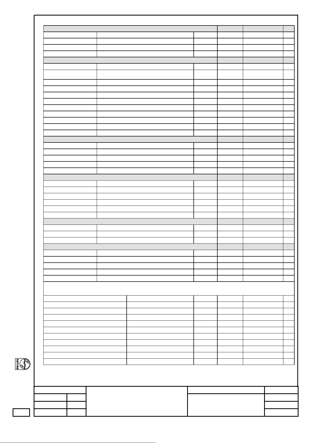
Feature Specification of MP3 CD
CODEC / COMPRESSION Format Compatibility
2011-04-01
1
2
3
CDSM WITH
MC127
SET SPECIFICATION
Page 7
√
√
√
√
)
√
√
√
√
√
√
√
√
√
MP3 X
MPEG 2.5 X
MP3 Pro X
WMA X
AAC X
Playback CAPACITY
Maximum number of
X
40
35
36
37
38
39
tracks per CD
Maximum number of
X
41
albums per CD
DISC TYPE
CD-RW
CD-R
8 cm
12 cm
DISC SIZE (MB
185
225
650
680
700
42
43
44
45
46
47
48
49
50
ISO-9660 + Joliet X
Joliet X
UDF (Direct CD from X
ID3 X
Packet writing X
51
52
53
54
55
Multi-session CDDA X
Multi-session MP3 X
Closed session
Open session
Finalized disc
Unfinalized disc
56
57
58
59
60
61
CDDA + MP3/WMA X
MP3/WMA + CDDA X
MP3/WMA + CDDA
X
62
63
64
+ MP3/WMA
CDDA + MP3/WMA
X
65
+ CDDA
Video + CDDA X
CDDA + Data X
MP3/WMA + Data X
66
67
68
2011-04-01
2
1
CDSM WITH
MC127
3
SET SPECIFICATION
Page 8
)
)
√
√
√
√
√
y
BITRATE (kbps
64 -192 X
8 – 320 X
Variable X
Sampling RATE (kHz
8 X
11.025 X
12 X
16 X
22.05
24 X
32 X
44.1 X
48 X
96 X
UPGRADE ABILITY
MP3 X
MP3 Pro X
WMA X
AAC X
SOUND
Single Channel
Dual Channel
Stereo & joint Stereo
Intensity Stereo
MS Stereo
LANGUAGE SUPPORT
English X
Chinese X
Playlist Compatibilit
WinAmp X
Realjukebox X
MS Mediaplayer X
MusicMatch X
X
70
71
72
73
74
75
76
77
78
79
80
81
82
83
84
85
86
87
88
89
90
91
92
93
94
95
96
97
2011-04-01
2
1
CDSM WITH
MC127
3
SET SPECIFICATION
Page 9
e
MEASUREMENT SETUP
Tuner FM
2-1
Bandpass
LF Voltmeter
e.g. PM2534
RF Generator
e.g. PM5326
DUT
250Hz-15kHz
e.g. 7122 707 48001
Ri=50:
S/N and distortion meter
e.g. Sound Technology ST1700B
Use a bandpass filter to eliminate hum (50Hz, 100Hz) and disturbance from the pilottone (19kHz, 38kHz).
Tuner AM (MW,LW)
RF Generator
e.g. PM5326
Ri=50:
DUT
Frame aerial
e.g. 7122 707 89001
Bandpass
250Hz-15kHz
e.g. 7122 707 48001
LF Voltmeter
e.g. PM2534
S/N and distortion meter
e.g. Sound Technology ST1700B
To avoid atmospheric interference all AM-measurements have to be carried out in a Faraday´s cage.
Use a bandpass filter (or at least a high pass filter with 250Hz) to eliminate hum (50Hz, 100Hz).
CD
Use Audio Signal Disc
(replaces test disc 3)
DUT
L
R
SBC429 4822 397 30184
S/N and distortion meter
e.g. Sound Technology ST1700B
LEVEL METER
e.g. Sennheiser UPM550
-
Recorder
Use Universal Test Cassette CrO2 SBC419 4822 397 30069
or Universal Test Cassette
LF Generator
e.g. PM5110
Fe SBC420 4822 397 30071
DUT
L
R
S/N and distortion met
e.g. Sound Technology ST170
LEVEL METER
e.g. Sennheiser UPM550
with FF-filter
Page 10

INSTRUCTIONS ON CD PLAYABILITY
Customer complaint
"CD related problem"
Set remains closed!
check playability
1
2 - 2
playability
ok ?
Y
Play a CD
for at least 10 minutes
check playability
playability
ok ?
Y
N
"fast" lens cleaning
check playability
playability
ok ?
N
3
N
Y
For flap loaders (= access to CD drive possible)
cleaning method
4 is recommended
add Info for customer
"SET OK"
2
return set
1 - 4 For description - see following pages
Exchange CDM
Page 11

INSTRUCTIONS ON CD PLAYABILITY
2 - 3
1
PLAYABILITY CHECK
For sets which are compatible with CD-RW discs
use CD-RW Printed Audio Disc....................7104 099 96611
TR 3 (Fingerprint)
TR 8 (600µ Black dot) maximum at 01:00
• playback of these two tracks without audible disturbance
playing time for: Fingerprint
Black dot from 00:50 to 01:10
• jump forward/backward (search) within a reasonable time
For all other sets
use CD-DA SBC 444A..................................4822 397 30245
TR 14 (600µ Black dot) maximum at 01:15
TR 19 (Fingerprint)
TR 10 (1000µ wedge)
• playback of all these tracks without audible disturbance
playing time for: 1000µ wedge 10seconds
Fingerprint 10seconds
Black dot from 01:05 to 01:25
• jump forward/backward (search) within a reasonable time
10seconds
4
LIQUID LENS CLEANING
Before touching the lens it is advised to clean the
surface of the lens by blowing clean air over it.
This to avoid that little particles make scratches on
the lens.
Because the material of the lens is synthetic and coated
with a special anti-reflectivity layer, cleaning must be done
with a non-aggressive cleaning fluid. It is advised to use
“Cleaning Solvent
The actuator is a very precise mechanical component and
may not be damaged in order to guarantee its full function.
Clean the lens gently (don’t press too hard) with a soft and
clean cotton bud moistened with the special lens cleaner.
The direction of cleaning must be in the way as indicated in
the picture below.
2
CUSTOMER INFORMATION
It is proposed to add an addendum sheet to the set which
informs the customer that the set has been checked
carefully - but no fault was found.
The problem was obviously caused by a scratched, dirty or
copy-protected CD. In case problems remain, the customer
is requested to contact the workshop directly.
The lens cleaning (method 3) should be mentioned in the
addendum sheet.
The final wording in national language as well as the printing
is under responsibility of the Regional Service Organizations.
Page 12

2.0 SAFTETY INSTRUCTIONS
WARNING
GB
All ICs and many other semi-conductors are
susceptible to electrostatic discharges (ESD).
Careless handling during repair can reduce life
drastically.
When repairing, make sure that you are
connected with the same potential as the mass
of the set via a wrist wrap with resistance.
Keep components and tools also at this
potential.
F
ATTENTION
Tous les IC et beaucoup d’autres
semi-conducteurs sont sensibles aux
décharges statiques (ESD).
Leur longévité pourrait être considérablement
écourtée par le fait qu’aucune précaution n’est
prise à leur manipulation.
Lors de réparations, s’assurer de bien être relié
au même potentiel que la masse de l’appareil et
enfiler le bracelet serti d’une résistance de
sécurité.
Veiller à ce que les composants ainsi que les
outils que l’on utilise soient également à ce
potentiel.
2-4
ESD
D
WARNUNG
Alle ICs und viele andere Halbleiter sind
empfindlich gegenüber elektrostatischen
Entladungen (ESD).
Unsorgfältige Behandlung im Reparaturfall kan
die Lebensdauer drastisch reduzieren.
Veranlassen Sie, dass Sie im Reparaturfall über
ein Pulsarmband mit Widerstand verbunden
sind mit dem gleichen Potential wie die Masse
des Gerätes.
Bauteile und Hilfsmittel auch auf dieses gleiche
Potential halten.
WAARSCHUWING
NL
Alle IC’s en vele andere halfgeleiders zijn
gevoelig voor electrostatische ontladingen
(ESD).
Onzorgvuldig behandelen tijdens reparatie kan
de levensduur drastisch doen verminderen.
Zorg ervoor dat u tijdens reparatie via een
polsband met weerstand verbonden bent met
hetzelfde potentiaal als de massa van het
apparaat.
Houd componenten en hulpmiddelen ook op
ditzelfde potentiaal.
I
AVVERTIMENTO
Tutti IC e parecchi semi-conduttori sono
sensibili alle scariche statiche (ESD).
La loro longevità potrebbe essere fortemente
ridatta in caso di non osservazione della più
grande cauzione alla loro manipolazione.
Durante le riparazioni occorre quindi essere
collegato allo stesso potenziale che quello della
massa dell’apparecchio tramite un braccialetto
a resistenza.
Assicurarsi che i componenti e anche gli utensili
con quali si lavora siano anche a questo
potenziale.
GB
Safety regulations require that the set be restored to its original
condition and that parts which are identical with those specified,
be used.
NL
Veiligheidsbepalingen vereisen, dat het apparaat bij reparatie in
zijn oorspronkelijke toestand wordt teruggebracht en dat onderdelen,
identiek aan de gespecificeerde, worden toegepast.
F
Les normes de sécurité exigent que l’appareil soit remis à l’état
d’origine et que soient utiliséés les piéces de rechange identiques
à celles spécifiées.
D
Bei jeder Reparatur sind die geltenden Sicherheitsvorschriften zu
beachten. Der Original zustand des Geräts darf nicht verändert werden;
für Reparaturen sind Original-Ersatzteile zu verwenden.
I
Le norme di sicurezza esigono che l’apparecchio venga rimesso
nelle condizioni originali e che siano utilizzati i pezzi di ricambio
identici a quelli specificati.
“Pour votre sécurité, ces documents
doivent être utilisés par des spécialistes agréés, seuls habilités à réparer
votre appareil en panne”.
CLASS 1
LASER PRODUCT
GB
Warning !
Invisible laser radiation when open.
Avoid direct exposure to beam.
S
Varning !
Osynlig laserstrålning när apparaten är öppnad och spärren
är urkopplad. Betrakta ej strålen.
Varoitus !
SF
Avatussa laitteessa ja suojalukituksen ohitettaessa olet alttiina
näkymättömälle laserisäteilylle. Älä katso säteeseen!
3122 110 03420
"After servicing and before returning set to customer perform a
DK Advarse !
leakage current measurement test from all exposed metal parts to
earth ground to assure no shock hazard exist. The leakage current
must not exceed 0.5mA."
Caution: These servicing instructions are for use by qualified service personnel only.
To reduce the risk of electric shock do not perform any servicing other than that contained in the operating instructions unless you are qualified to do so.
Usynlig laserstråling ved åbning når sikkerhedsafbrydere er
ude af funktion. Undgå udsaettelse for stråling.
Page 13

2-5
2.1 ESD PROTECTION
Whenthepowersupplyisbeingturnedon,youmaynotremovethislasercautionslabel.Ifitremoves,radiationoflaser
maybereceived.
PREPARATIONOFSERVICING
PickupHeadconsistsofalaserdiodethatisverysusceptibletoexternalstaticelectrocity.
Althoughitoperatesproperlyafterreplacement,ifitwassubjecttoelectrostaticdischargeduringreplacement,
itslifemightbeshortened.Whenreplacing,useaconductivemat,solderingironwithgroundwire,etc.to
protectthelaserdiodeform
Andalso,theLSIandICaresameasabove.
Solderingiron
withgroundwire
orceramictype
damagebystaticelectricity.
Groundconductive
wriststrapforbody.
Conductivemat
1M
Thegroundresistance
betweenthegroundline
andthegroundislessthan10
Page 14

SAFTY NOTICE
LEAKAGE CURRENT CHECK
2-6
SAFTY PRECAUTIONS
Plug the AC line cord directly into a 120V AC outlet (do
not use an isolation transformer for this check). Use an
AC voltmeter, having 5000 per volt or more sensitivity.
Connect a 1500 10W resistor,paralleled by a 0.15uF
150V AC capacitor between a knomn good earth ground
(water pipe, conduit, etc.) and all exposed metal parts of
cabinet (antennas, handle bracket, metal cabinet
screwheads, metal overlays, control shafts, etc.).
READING SHOULD NOT EXCEED 0.3V
DVD VIDEO PLAYER
Measure the AC voltage across the 1500 resistor.
The test must be conducted with the AC switch on and
then repeated with the AC switch off. The AC voltage
indicated by the meter may not exceed 0.3V.A reading
exceeding 0.3V indicates that a dangerous potential
exists, the fault must be located and corrected.
Repeat the above test with the DVD VIDEO PLAYER
power plug reversed.
NEVER RETURN A DVD VIDEO PLAYER TO THE
CUSTOMER WITHOUT TAKING NECESSARY
CORRECTIVE ACTION.
AC VOLTMETER
(5000 per volt
or more sensitivity)
Good earth ground
1500
10W
such as a water pipe,
conduit, etc.
AC OUTLET
0.15uF 150V AC
Test all exposed metal.
Voltmeter Hook-up for Leakage Current Check
The lightning flash with arrowhead symbol, within an
equilateral triangle, is intended to alert the user to the
presence of uninsulated "dangerous voltage" within the
product's enclosure that may be of sufficient magnitude to
constitute a risk of electric shock to persons.
The exclamation point within an equilateral triangle is
intended to alert the user to the presence of important
operating and maintenance (servicing) instructions in the
literature accompanying the appliance.
Page 15

2-7
2.2 SAFETY INSTRUCTIONS
Battery Handling Guideline
Since the battery is packed in soft package, to ensure its better performance, it’s very important to carefully handle
the battery
2.2.1 Soft Aluminium foil
The soft aluminum packing foil is very easily damaged by sharp edge parts such as Ni-tabs, pins and needles.
• Don’t strike battery with any sharp edge parts
• Trim your nail or wear glove before taking battery
• Clean worktable to make sure no any sharp particle
2.2.2 Sealed edge
Sealing edge is very flimsy
• Don’t bend or fold sealing edge
2.2.3 Folding edge
The folding edge is form in battery process and passed all hermetic test.
• Don’t open or deform folding edge
2.2.4 Tabs
The battery tabs are not so stubborn especially for aluminum tab.
• Don’t bend tab
2.2.5 Mechanical shock
• Don’t Fall, hit, bend battery body
2.2.6 Short
Short terminals of battery is strictly prohibited, it may damage battery.
Caution: Danger of explosion if battery is incorrectly replaced.
Replace only with the same or equivalent type.
Page 16

Disassemble diagrams:
!
Notes: don t touch the power board when the machine is power on, pls unplug the power cord then disassemble the machine to avoid shock!!
1-C
1-D
2.6X8PB screws on
two
2.6X8PBscrewson
Notes: don't touch the power board when the machine is power on, pls unplug the power cord then disassemble the machine to avoid shock!
1、Disassemble the front cabinet
1-A 1-B
disassemble the two 3*8 KB screws on two side
cabinet
unplug the 3pin and 10pin cable which connecting to
MP3-LINK BD and display BD,remove the front cabinet
disassemble the two 3*25 PB screws on
bottom cabinet
disassemble the nine
disply BD and get out
disassemble the
LINKBDandgetoutthe
open the front cabinet
Page 17

2、Disassemble the top cabinet and Main BD
p
disassemble the two
38
unplug the 2pin cable
,
,
2-A 2-B 2-C
disassemble the two 3*8
PBscrewsons‐video
PBscrewsons‐videoport
ort
disassemble the three
3*8PBscrewsonbottom
3*8PBscrewsonbottom
cabinet
unplug the 2pin cable
between Main BD and
between Main BD and
power BD
45°put up top cabinet
and Main BD
unplug the FM-ANT
unplug the FM-ANT
line and apart it from
bottom cabinet
1
2
disassemble the five
2.6X8PB screws on
Main BD
unplug the open-close
cable,6pin cable to CD
deck,FFC cable on CD
take out the Main BD
deck
2-E disassemble CD deck 2-F disassemble CD door2-D disassemble Main BD
disassemble the four 2.6X8PWAscrews
onCDdeckandtakeoutit
take out the spring first ,then remove the
fastener on two CD door sides and
remove the CD door
Page 18

3、Disassemble the power BD
pg p
disassemble the two
3*10 PWB screws on
power BD
unplug the power cord and take out
the PCB
Page 19

SET BLOCK DIAGRAM
3 - 1
3 - 1
Page 20

SET WIRING DIAGRAM
4 - 1 4- 1
Page 21

CIRCUIT DIAGRAM - DISPLAY+MAIN+TUNER+LINE IN board
PART 1
R3381KR338
R348
R348
6.8K
6.8K
R346
R346
4.7K
4.7K
R3391KR339
R378
R378
100R
100R
R347
R347
C333
C333
4.7K
4.7K
102P
102P
1K
1K
C326
C326
0.1uF
0.1uF
ZD306
ZD306
6V8
6V8
C334
C334
102P
102P
RAR-CH
CDR-CH
CD/L
CD/R
JK601
JK601
Line Jack
Line Jack
R353
R353
4.7K
4.7K
R349
R349
CN302CN302
AUX-RIN
GND
AUX-LIN
7314_SDA
7314_SCL
C3651UC365
1U
C3661UC366
1U
+7.5V
R345
R345
6.8K
6.8K
CDL-CH
R351
R351
4.7K
4.7K
6.8K
6.8K
R352
R352
6.8K
6.8K
CDR-CH
R602NCR602
C602
C602
CN601CN601
220P
223P
223P
C604
C604
C605
C605
223P
223P
C6011UC601
C6071UC607
L601
L601
1U
10.5T
10.5T
L603
L603
10.5T
10.5T
L602
L602
10.5T
10.5T
1U
R601
R601
R603
R603
33K
33K
220P
NC
TO CN302
33K
33K
R606NCR606
AUX-RIN
GND
AUX-LIN
C603
C603
220P
220P
NC
TO CN306
LINE BD
R337
R337
47K
47K
C325
C325
100uF/16V
100uF/16V
C3361UC336
C335
C335
C3481UC348
C3421UC342
C3431UC343
C339
C339
C3461UC346
C338
C338
1500P
1500P
C337
C337
1500P
1500P
R336
R336
47K
47K
0.1uF
0.1uF
0.1uF
0.1uF
5 - 15 - 1
MAIN SIGNAL
AUX SIGNAL
RADIO SIGNAL
CD SIGNAL
R325
C320NCC320
NC
R326
R326
4.7K
4.7K
R334
R334
10K
10K
C349
C349
22uF/16V
22uF/16V
R327
R327
4.7K
4.7K
C323NCC323
NC
R335
R335
10K
10K
R325
10K
10K
S9014
S9014
Q311
Q311
A9014
A9014
C3141UC314
Q312
Q312
C3171UC317
1U
R3281KR328
1K
C318
R3291KR329
C318
152M
152M
C316
C316
100uF/10V
C319
C319
152M
152M
R33082R330
R31882R318
100uF/10V
82
82
C312
C312
220uF/16V
220uF/16V
100uF/10V
100uF/10V
1K
R3191KR319
1K
R3201KR320
1K
1U
OUT-L
NC
NC
C367NCC367
C340NCC340
IC302
IC302
SC7314
SC7314
C327
C327
C324
C324
0.1uF
0.1uF
C3211UC321
1U
C3221UC322
C3471UC347
C328
C328
C329
C329
C330
C330
C331
C331
C3321UC332
C3411UC341
1U
0.12uF
0.12uF
0.12uF
0.12uF
0.12uF
0.12uF
0.12uF
0.12uF
1U
1U
1U
1U
1U
1U
1U
1U
R342
R342
5.6K
5.6K
R340
R340
5.6K
5.6K
22uF/16V
22uF/16V
CDL-CH
RAL-CH
OUT-L
OUT-R
MUTE
CD-MUTE
OUT-R
D302
D302
1N4148
1N4148
C313
C313
IC301
IC301
UTC8227
UTC8227
0.015uF
0.015uF
C309
C309
0.015uF
0.015uF
C307
C307
C311
C311
C315
C315
100uF/16V
100uF/16V
100uF/16V
100uF/16V
R317
R317
R316
R316
2.2
2.2
L304
C306
C306
470uF/16V
470uF/16V
L304
4R7UH/2A
4R7UH/2A
2.2
2.2
SPEAKER OUTPUT
TO MAIN PWB CN304
C302
C308
C308
470uF/16V
470uF/16V
C302
223P
223P
C301
C301
223P
223P
L306
L306
4R7UH/2A
4R7UH/2A
L305
L305
4R7UH/2A
4R7UH/2A
+
L.SP
-
8 OHM 2W
R.SP
+
8 OHM 2W
+12V
+7.5V
C396
C396
0.1UF
0.1UF
R788
R788
C310
R311
R311
2.2 1/2W
2.2 1/2W
Q306
Q306
8550
8550
R313
R313
2.2K
2.2K
330U/16V
330U/16V
Q307
Q307
9014C
9014C
C310
C304
C304
1000uF/16V
1000uF/16V
C351
C351
0.1UF
0.1UF
+12V
+12V
GND
CN303CN303
TO CN1102
R3501KR350
LED_EN
IC102
47uF/16V
47uF/16V
D703
D703
1N5819
1N5819
IN
IN
C107
C107
0.1U
0.1U
IC102
1117/3.3
1117/3.3
R309
R309
22K
22K
GND
GND
Q305
Q305
B772
B772
OUT
OUT
R305
R305
33K
33K
R306
R306
1.5K
1.5K
Q304
Q304
9014C
9014C
GND
C106
C106
0.1uF
0.1uF
D301
D301
IN4001
IN4001
C120
C120
TU+3.3V
100uF/16V
100uF/16V
C394
C394
223
223
+7.5V
IC402
IC402
OUT
LS7805
LS7805
IC705
IC705
GND
GND
GND
GND
OUT
OUT
OUT
C729
C729
C709
C709
0.1uF
0.1uF
C707
C707
47uF/50V
47uF/50V
563M
563M
MCU_3V3
C728
C728
100uF/16V
100uF/16V
VCC+5V
IN
C305A
C305A
C724
C724
100uF/16V
100uF/16V
100uF/16V
100uF/16V
IN
IN
C769
C769
IN
C725
C725
0.1U
0.1U
ESD
ESD
1117/3.3V
1117/3.3V
R741
R741
100
100
100
100
RA-VDD
CDVCC
CD-EN
R310
R310
10K
10K
10uF/16V
10uF/16V
C386
C386
C108
C108
MCU_3V3
RA-VDD
TUNER-EN
Q703
Q703
8550B/C
8550B/C
R107
R107
100UH
100UH
R308
R308
10K
10K
R760
R760
4.7K
4.7K
MAIN_EN
C385
C385
C156
C156
0.1uF
0.1uF
GND
R321
R321
4.7K
4.7K
C368
C368
100uF/16V
100uF/16V
10uF/16V
10uF/16V
R307
R307
Q302
Q302
8550B/C
8550B/C
22K
22K
R394
R394
R304
R304
33K
33K
2.2K
2.2K
Q303
Q303
9014C
9014C
R303
R303
R332
R332
2.2K
2.2K
Q308
Q308
9014
9014
+7.5V
R392
R392
2.2 1/2W
2.2 1/2W
33K
33K
C350
C350
1000uF/10V
1000uF/10V
C303
C303
MAIN-EN
Q309
Q309
8550B/C
8550B/C
47uF/16V
47uF/16V
C402
C402
0.1uF
0.1uF
R315
R315
4.7K
4.7K
C305
C305
10uF/16V
10uF/16V
1K
Q310
Q310
D882
D882
R312
R312
680
680
ZD302
ZD302
8.2V
8.2V
R314
R314
22K
22K
Page 22

5 - 2 5 - 2
CIRCUIT DIAGRAM - DISPLAY+MAIN+TUNER+LINE IN board
PART 2
C797
C797
473P
473P
Q901
Q901
B764
B764
+5V
C919
C919
C901
C901
C920
C920
C923
MOTOSPMOTO
C958
C958
10P
10P
C923
104
104
102
102
R940
R940
10K
10K
SA9258
SA9258
IC901
IC901
SP
R912
R912
15K
15K
R914
R914
15K
15K
R922
R922
15K
15K
R924
R924
15K
15K
R926
R926
68K
68K
R928
R928
68K
68K
C929
C929
C931
C931
C936
C936
220P
220P
220P
220P
220P
220P
C917
C917
R901
R901
47UF
47UF
22R
22R
Q902
C961
C961
Q902
8550
8550
R937
R937
10R
10R
C963
C963
104
104
R944
R944
56K
56K
R943
R943
56K
56K
R942
R942
56K
56K
R941
R941
56K
56K
C955
C955
104
104
C962
C962
10P
10P
10P
10P
RFGND
C965
C965
104
104
R948
R948
R950NCR950
47K
47K
NC
C939
C939
220P
220P
LD
MON
RFM
REF
RFG
C906
C906
470UF
470UF
C932
C932
473P
473P
GND
SL
MOTOSLMOTO
R911
R911
10K
10K
R913
R913
10K
10K
R921
R921
10K
10K
R923
R923
10K
10K
R925
R925
10K
10K
R927
R927
10K
10K
C942
C942
C945
C945
220P
220P
220P
220P
R951NCR951
R952
R952
NC
47K
47K
VDD
RFC
LDON
BST
SA9614
RFRC
PD
GND
C972
C972
C970
C970
RFI
RFO
C971
C971
EQIN
IC903IC903
RFAC
R960
R960
2.2K
2.2K
18P
18P
R956NCR956
NC
R957NCR957
104P
104P
103P
103P
C928
C928
220P
220P
NC
R9591MR959
1M
TO CD DEDK
FCSTR+
TR-
FCS+
PD
GND
LD
GND
F
C
B
A
D
E
VCC
VC
CN902CN902
C957
C957
104
104
C968
C968
104
104
220UF
220UF
9258-MUTE
C966
C966
10P
10P
10P
10P
SW901
SW901
SLED_SW
SLED_SW
C910
C910
C911
C911
47UF
47UF
47UF
47UF
C946
C946
104
104
C959
C959
10P
10P
C930
C930
220P
220P
C991
C991
RFGND
C915
C915
C909
C909
3.3UF
3.3UF
104
104
1UF
1UF
C975
C975
473P
473P
C935
C935
220P
220P
R9581KR958
1K
C916
C916
100UF
100UF
C922
C922
R916
R929
R929
100K
100K
+5V
X901
X901
8.4672M
8.4672M
R902NCR902
R916
R917
R917
R918
R918
R919
R919
NC
C904
C904
47U
47U
R935
R935
330
330
C952
C952
22P
22P
9258-MUTE
10K
10K
R555ED
R555ED
8.2K
8.2K
8.2K
8.2K
22k
22k
10K
10K
DGND
10K
10K
R555CD
R555CD
+5V
R966
R966
L-OUT
R-OUT
R904
R9541KR954
PAGND
C1
104C1104
1K
+5V
R904
4.7K
4.7K
C921
C921
102
102
C974
C974
3900P
3900P
PAGND
PAGND
+5V
C914
C914
220UF
220UF
R965
R965
CD-MUTE
10K
10K
D2
R11KR1
1K
IN4148D2IN4148
C2
104C2104
PAGNDPAGND
+5V
C978
C978
104
104
C992
C992
104
104
CD-DATA
26UH
26UH
L901
L901
L-OUT
R-OUT
PAGND
CD-DATA
CD-CLOCK
CD-MUTE
VCC
GND
VCC
GND
L-OUT
R-OUT
PGND
CD-DATA
CD-CLOCK
CD-MUTE
CN903CN903
TO CN305
VCC
GND
CD PWB
C913
C913
47UF
47UF
R955
R955
10K
10K
D904
D904
1N4148
1N4148
C993
C993
R909
R909
103
103
8.2K
8.2K
C933
C933
104
104
C902
C902
10UF
10UF
C940
C940
222
222
IC902
IC902
SC9640
SC9640
33K
33K
R947
R947
R945
R945
33K
33K
33K
33K
R939
R939
100K
100K
R962
R962
100
100
D906NCD906
D905NCD905
NC
NC
C943
C943
222
222
R915
R915
8.2K
8.2K
C903
C903
10UF
10UF
C907
C907
10UF
10UF
C995
C995
103
103
PAGND
C912
C912
47U
47U
C908
C908
47UF
47UF
CN901NCCN901
C967
C967
NC
104
104
R910
R910
4.7K
4.7K
R961
R961
10K
10K
CD-COLCK
C964
C964
104P
104P
C948
C948
104
104
PAGND
R934
R934
Q903
Q903
9014C
9014C
CN904
CN904
DOOR SW
DOOR SW
C937
C937
102
102
10R
10R
R949
R949
10K
10K
R905
R905
8.2K
8.2K
R906
R906
8.2K
8.2K
R9300RR930
R907
R907
R908
R908
104
104
+5V
C941
C941
C938
C918
C918
47UF
47UF
C938
220P
220P
R946
R946
C969
C969
220P
220P
104
104
150K
150K
C944
C944
220P
220P
R953
R953
2.2R
2.2R
0R
5.6K
5.6K
2.7K
2.7K
C926
C927
C927
R920
R920
C926
105
105
104
104
2.2R
2.2R
R931
R931
22K
22K
C947
C947
104
104
D907
D907
1N4148
1N4148
C934
C934
C924
C924
C925
C925
332
332
332
332
R903NCR903
C953
C953
104P
104P
R933
R933
68K
68K
C951
C951
22P
22P
C950
C950
223P
223P
NC
D908
D908
1N4148
1N4148
C905
C905
104
104
47U
47U
C949
C949
20P
20P
R9321KR932
1K
C954
C954
472P
472P
Page 23

5 - 3 5 - 3
CIRCUIT DIAGRAM - DISPLAY+MAIN+TUNER+LINE IN board
PART 3
LED[0..20]
LED1
LED2
LED3
IC701
IC701
LED4
LED5
LED6
LED7
ET6202
ET6202
51K
51K
R713
R713
GND
LED_CLK
LED_STB
LED_RESET
LED_RESET
LED_CLK
LED_STB
GND
TU_RESET
TU_SDA
TU_SCL
TU_RESET
POWER_EN
LED13
LED14
100
100
R702
R702
LED_CLK
LED_RESET
TU_SDA
TU_SCL
CD_EN
TU_EN
R701
R701
100
100
LED703LED703
LED6
100
100
R714
R714
C708
C708
LED_STB
C702
C702
C703
C703
C701
C701
GND
C731
C731
GND
GND
GND
1000P
1000P
LED7
R706
R706
R716
R716
R715
R715
C732
C732
FM/ANT
KEY1
D103
D103
BAV99
BAV99
GND
C109
C109
C714
C714
30P
30P
6.8K
R725
R725
R724
SW713A
SW713A
R724
SW711
SPK+SPK+
3.3K
3.3K
R727
PLAY/PAUSE
PLAY/PAUSE
R727
STOP
STOP
SW712A
SW712A
R729
102P
102P
R729
33K
33K
MCU_3V3
R868
R868
R869
R869
SW710
SW708
SPK-SPK-
REPEATREPEAT
SW709
DBBDBB
22K
22K
15k
15k
10K
10K
6.8K
248-M12703-100
D702
D702
Q702
Q702
R741
R741
8050
8050
1N4148
R4NCR4
NC
Y1
32.768KHZY132.768KHZ
C2
22PC222P
IC101
IC101
Si7404
Si7404
R1061KR106
1K
C112
C112
102P
102P
C104
C104
C116
C116
220P
220P
100/100
100/100
104PC3104P
C117
C117
C3
220P
220P
R110
R110
1N4148
C114
C114
C115
C115
R745
R745
10K
10K
7.5K
7.5K
7.5K
7.5K
100
100
MCD_3V3
C102
C102
104P
104P
C1
22PC122P
R1
10RR110R
C113
C113
100
100
22P
22P
R108
R108
68P
68P
C120
C120
R111
R111
2.2
2.2
LED701LED701
Q701
Q701
8050
8050
R730
R730
10K
10K
C118
C118
8200P
8200P
10K
10K
LED_EN
GND
GND
R753
R753
10K
10K
GND
RAL-CH
RAR-CH
C119
C119
8200P
8200P
TU+3.3V
R105
R105
10K
10K
TU_SDA
TU_SCL
TU_RST
MCU_3V3
GND
C705
C705
0.1uF
0.1uF
C713
C713
GND
10K
10K
47P
47P
10K
10K
47P
47P
10K
10K
47P
47P
1000P
1000P
C730
C730
R748
R748
10K
10K
R746
R746
10K
10K
R750
R750
10K
10K
R758
R758
330K
330K
R760
R760
10K
10K
R759
R759
10K
10K
R751
R751
10K
10K
0.1uF
0.1uF
100uF/16V
100uF/16V
R762
R762
100
100
R761
R761
100
100
LED12
VCC+5V
MCU_3V3
1000P
1000P
LED11
LED1
LED2
MCU_3V3
MCU_3V3
MCU_3V3
MCU_3V3
MCU_3V3
MCU_3V3
MAIN_EN
MCU_3V3
MCU_3V3
LED3
LED8
LED10
LED4
LED9
LED5
LED10
LED8
LED11
LED9
LED12
LED13
LED14
TU_EN
R957
R957
CD_DATA
R810
R810
R836
R836
22K
22K
33K
33K
VOL-
VOL-
F.R
F.R
SW810A
SW810A
SW811A
SW811A
KEY2
R838
R838
R833
SW815A
SW815A
SOURCE
SOURCE
R833
R858
R858
3.3K
3.3K
6.8K
6.8K
PRESET-
PRESET-
SW814A
SW814A
R835
R835
15K
15K
10K
10K
DBB
DBB
PRESET+
PRESET+
SW812A
SW812A
SW813A
SW813A
R8590RR859
POWER
POWER
SW816A
SW816A
0R
R802
R802
C804
C804
102P
102P
33K
33K
248-M12705-100
MCU_3V3
C726
C726
47U
47U
C727 0.1UC727 0.1U
IC703
IC703
M24C02
M24C02
REMOTE/AC_DET
R749
R749
4K7
4K7
*
KEY2
KEY1
15P
X701
X701
32.768KHz
32.768KHz
JW9260RJW926
R742
R742
330K
330K
MCU_3V3
0R
C718
C718
R733
R733
R734
R734
R732
R732
270K
270K
IC702
IC702
SC9309
SC9309
D302
D302
1n4148
2.2K
2.2K
2.2K
2.2K
R956
R956
R861
R861
1K8
1K8
CD_EN
CD_CLK
POWER_EN
R860
R860
1K8
1K8
7314_SCL
7314_SDA
MUTE
1n4148
R743
R743
330K
330K
15P
C712
C712
15P
15P
C715
C715
MCU_3V3
C717
C717
220P
220P
22P
22P
330K
330K
330K
330K
103P
103P
C719
C719
Q202
Q202
9014
9014
R740
R740
10K
10K
D301
D301
1N4148
1N4148
1M
103P
103P
R7361MR736
C720
C720
330K
330K
R855
R855
330K
330K
R854
R854
C721
C721
3.3UF
3.3UF
R737
R737
R738
R738
47K
47K
10K
10K
100K
100K
R739
R739
REMOTE
P801
P801
FM-6038TM2-5A
FM-6038TM2-5A
L813L813
MCU_3V3
IR
C722
C722
100UF
100UF
R21KR2
1K
R198
R198
100R
100R
C204
C204
104
104
8765
8765
VCC
R722
R722
4K7
4K7
WC
*
R7441KR744
SCL
SDA
1K
C723
C723
104P
104P
MCU_3V3
TU_SCL
TU_SDA
MCU_3V3
E0
E1
E2
VSS
4321
4321
Page 24

5 - 4
LAYOUT DIAGRAM - DISPLAY+MAIN+TUNER+LINE IN board
5 - 4
Page 25

CIRCUIT DIAGRAM - POWER BOARD
D1104
12
3 4
12
12
3 4
D1104
IN4007
IN4007
D1103
D1103
IN4007
IN4007
X1102
X1102
0.22/275V
0.22/275V
RV1101
RV1101
471K
471K
R1103
R1103
R1104
R1104
X1101
X1101
750K
750K
750K
750K
0.22/275V
0.22/275V
D1101 IN4007D1101 IN4007
IN4007
IN4007
D1102
D1102
LF1104
LF1104
54mH
54mH
R1101
R1101
750K
750K
R1102
R1102
750K
750K
NTC1101 5D-9NTC11015D-9
54mH
54mH
LF1101
LF1101
1 2
1 2
6 - 1 6 - 1
C1103
C1103
68UF/450V
68UF/450V
+
+
103
103
FR107
FR107
D1108
D1108
C1111
C1111
R1B2MR1B
R1A2MR1A
EC1101
EC1101
12
+
+
12
2M
2M
330P
330P
47UF/25
47UF/25
12
C1112
C1112
C1101
C1101
222/1KV
222/1KV
330P
330P
12
C1113
C1113
100K
100K
R1119
R1119
IC1101
IC1101
1
2
3
4 5
LC1209
LC1209
10K
10K
C1104
C1104
R1132
R1132
12
R1118
R1118
8
7
6
104
104
ZD1101
ZD1101
U1101
U1101
100K
100K
D1109
D1109
FR107
FR107
7V5
7V5
PC817B
PC817B
R1122
R1122
R1123
R1123
1
0R
0R
0R
0R
R1134
R1134
1 R1/2W
1 R1/2W
PT1101
PT1101
D1003
D1003
1
5 6
3
2
2
PC817B1PC817B1
4
R1108
R1108
3
C1105
C1105
2.2K
2.2K
10
8
3
1
R1117
R1117
NC
NC
D1113
D1113
D1110
D1110
SR3100
SR3100
EC1105
EC1105
1000UF/25V
1000UF/25V
1UF
1UF
12
U1102
U1102
TL431
TL431
2
R1105
R1105
C1119
C1119
47K
47K
NC
NC
NC
NC
R1110
R1110
12
+
+
10K
10K
2.7K
2.7K
R1107
R1107
+12V
EC1106
R23A
R23A
NC
NC
+
+
EC1106
1000UF/25V
1000UF/25V
+
+
NC
NC
R23B
R23B
CY1101
CY1101
1 2
0.0022UF/400V
0.0022UF/400V
CY1102
CY1102
1 2
0.0022UF/400V
0.0022UF/400V
3uH
3uH
L1103
L1103
1 2
3 4
LF1103
LF1103
54mH
54mH
C1115
C1115
0.1uF
0.1uF
C1116
C1116
0.01uF
0.01uF
1000UF/25V
1000UF/25V
+
+
EC1107
EC1107
1
2
CN1102CN1102
GND
+12V
1
AC~IN
AC1101AC1101
100R
100R
R1106
2
FS1101
FS1101
T1.6A L250V
T1.6A L250V
R1106
+12V
EC1108
EC1108
470UF/25
470UF/25
Page 26

LAYOUT DIAGRAM - POWER BOARD
6 - 2 6 - 2
Page 27

EXPLODED VIEW DIAGRAM
7 - 1 7 - 1
SPK
PCBA3
PCBA1
PCBA4
PCBA5
 Loading...