

Philips mb2646 DATASHEETS

Philips Semiconductors Products
Product specification
MB2646
Dual octal bus transceiver/registers (3-State)
1
August 23, 1993 853-1617 10589
FEATURES
•Independent registers for A and B buses
•Multiple V
CC
and GND pins minimize
switching noise
•Live insertion/extraction permitted
•Power-up 3-State
•Power-up reset
•Multiplexed real-time and stored data
•Outputs sink 64mA and source 32mA
•Latch-up protection exceeds 500mA per
Jedec JC40.2 Std 17
•ESD protection exceeds 2000V per MIL
STD 883 Method 3015 and 200V per
Machine Model
DESCRIPTION
The MB2646 high-performance BiCMOS
device combines low static and dynamic
power dissipation with high speed and high
output drive.
The MB2646 dual transceiver/register
consists of two sets of bus transceiver
circuits with 3-State outputs, D-type flip-flops,
and control circuitry arranged for multiplexed
transmission of data directly from the input
bus or from the internal registers. Data on the
A or B bus will be clocked into the registers
as the appropriate clock pin goes High.
Output Enable (nOE
) and Direction (nDIR)
pins are provided to control the transceiver
function. In the transceiver mode, data
present at the high impedance port may be
stored in either the A or B register or both.
QUICK REFERENCE DATA
SYMBOL PARAMETER
CONDITIONS
T
amb
= 25°C; GND = 0V
TYPICAL UNIT
t
PLH
t
PHL
Propagation delay
nAx to nBx
CL = 50pF; VCC = 5V 3.2 ns
C
IN
Input capacitance VI = 0V or V
CC
4 pF
C
I/O
I/O capacitance VO = 0V or VCC; 3-State 7 pF
I
CCZ
Total supply current Outputs disabled; VCC = 5.5V 500 µA
ORDERING INFORMATION
PACKAGES TEMPERATURE RANGE ORDER CODE DRAWING NUMBER
52-pin plastic Quad Flat Pack -40°C to +85°C MB2646BB 1418B
PIN CONFIGURATION LOGIC SYMBOL
Vcc Vcc
19 2220 231716 25 26241514 2118
1A2
1A3
1A4
GND
1A5
1A6
1A7
2A0
2A1
2A2
2A3
2A4
2A5
1
2
3
4
5
6
7
8
9
10
11
12
13
47 4446 434950 41 40425152 4548
1B2
1B3
1B4
1B5
1B6
1B7
2B0
2B1
2B2
GND
2B3
2B4
2B5
39
38
37
36
35
34
33
32
31
30
29
28
27
MB2646
52-pin PQFP
1A1
1A0
1SAB
1CPAB
1DIR
1OE
1CPBA
1SBA
GND
1B0
1B1
Vcc
2A6
2A7
GND
2SAB
2CPAB
2DIR
2OE
2CPBA
2SBA
2B7
2B6
Vcc
42 41 39 38 37 36 35 34
1B0 1B1 1B2 1B3 1B4 1B5 1B6 1B7
50 51 1 2 3 5 6 7
1A0 1A1 1A2 1A3 1A4 1A5 1A6 1A7
48
49
1CPAB
1SAB
47 1DIR
45 1CPBA
33 32 31 29 28 27 25 24
2B0 2B1 2B2 2B3 2B4 2B5 2B6 2B7
8 9 10 11 12 13 15 16
2A0 2A1 2A2 2A3 2A4 2A5 2A6 2A7
19
18
2CPAB
2SAB
20 2DIR
22 2CPBA
44 1SBA
46 1OE
23 2SBA
21 2OE
Philips Semiconductors Products Product specification
MB2646
Dual octal bus transceiver/registers (3-State)
August 23, 1993
2
DESCRIPTION (continued)
The select (nSAB, nSBA) pins determine
whether data is stored or transferred through
the device in real-time. The nDIR determines
which bus will receive data when the nOE
is
active Low. In the isolation mode (nOE
=
High), data from Bus A may be stored in the
B register and/or data from Bus B may be
stored in the A register. When an output
function is disabled, the input function is still
enabled and may be used to store and
transmit data. Only one of the two buses, A
or B may be driven at a time.
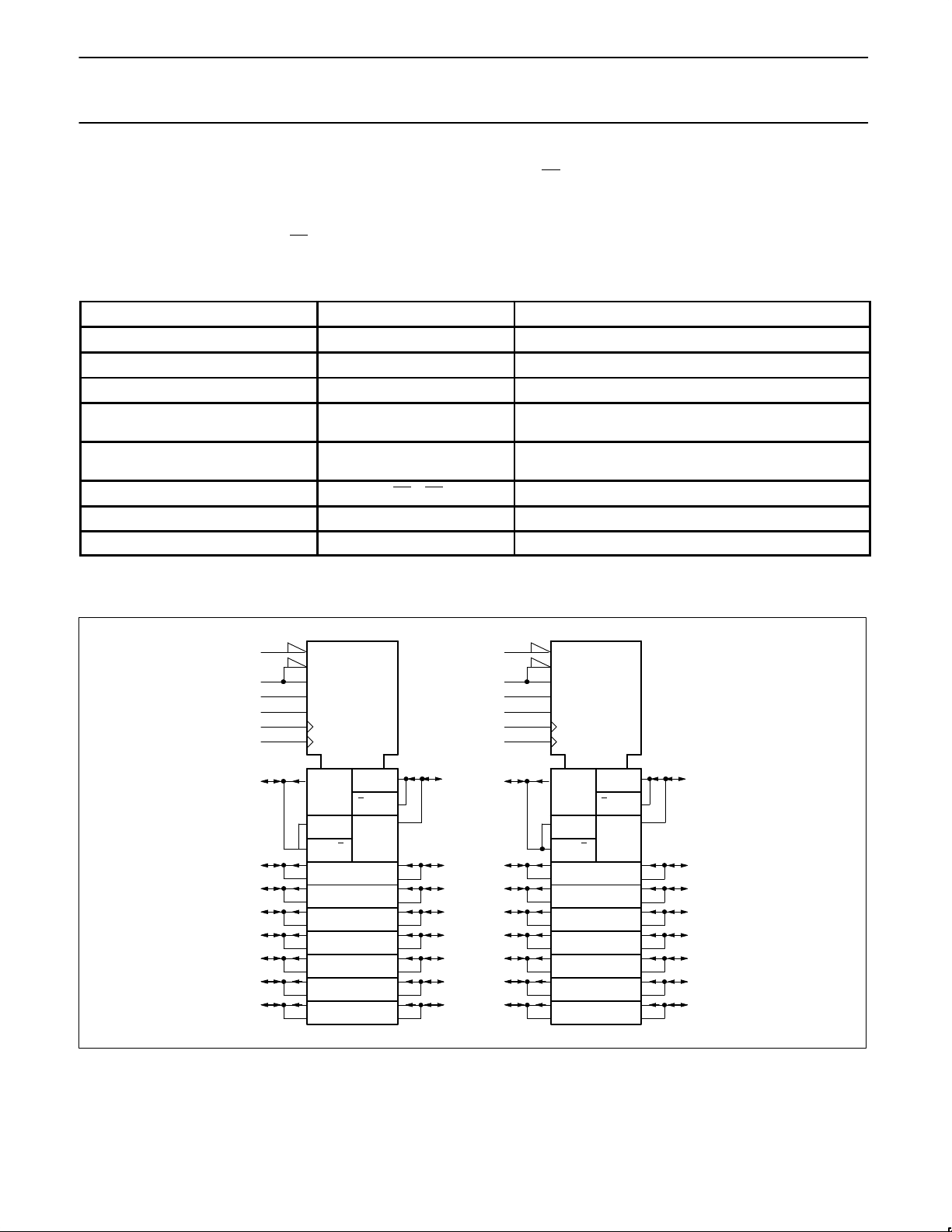
PIN DESCRIPTION
PIN NUMBER SYMBOL NAME AND FUNCTION
48, 45, 19, 22 1CPAB, 1CPBA, 2CPAB, 2CPBA Clock input A to B / Clock input B to A
49, 44, 18, 23 1SAB, 1SBA, 2SAB, 2SBA Select input A to B / Select input B to A
47, 20 1DIR, 2DIR Direction control inputs
50, 51, 1, 2, 3, 5, 6, 7,
8, 9, 10, 11, 12, 13, 15, 16
1A0 – 1A7,
2A0 – 2A7
Data inputs/outputs (A side)
42, 41, 39, 38, 37, 36, 35, 34,
33, 32, 31, 29, 28, 27, 25, 24
1B0 – 1B7,
2B0 – 2B7
Data inputs/outputs (B side)
46, 21 1OE, 2OE Output enable inputs
4, 17, 30, 43 GND Ground (0V)
14, 26, 40, 52 V
CC
Positive supply voltage
LOGIC SYMBOL (IEEE/IEC)
50
41
39
38
37
36
35
34
46
47
44
49
45
48
51
1
2
3
5
6
7
42
8
32
31
29
28
27
25
24
21
20
23
18
22
19
9
10
11
12
13
15
16
33
≥1
∇1
G3
3EN1 [BA]
3EN2 [AB]
G6
G7
C4
C5
5D 7
1 7
6 4D
6
1
≥1
2∇
≥1
∇1
G3
3EN1 [BA]
3EN2 [AB]
G6
G7
C4
C5
5D 7
1 7
6 4D
6
1
≥1
2∇
Philips Semiconductors Products Product specification
MB2646
Dual octal bus transceiver/registers (3-State)
August 23, 1993
3
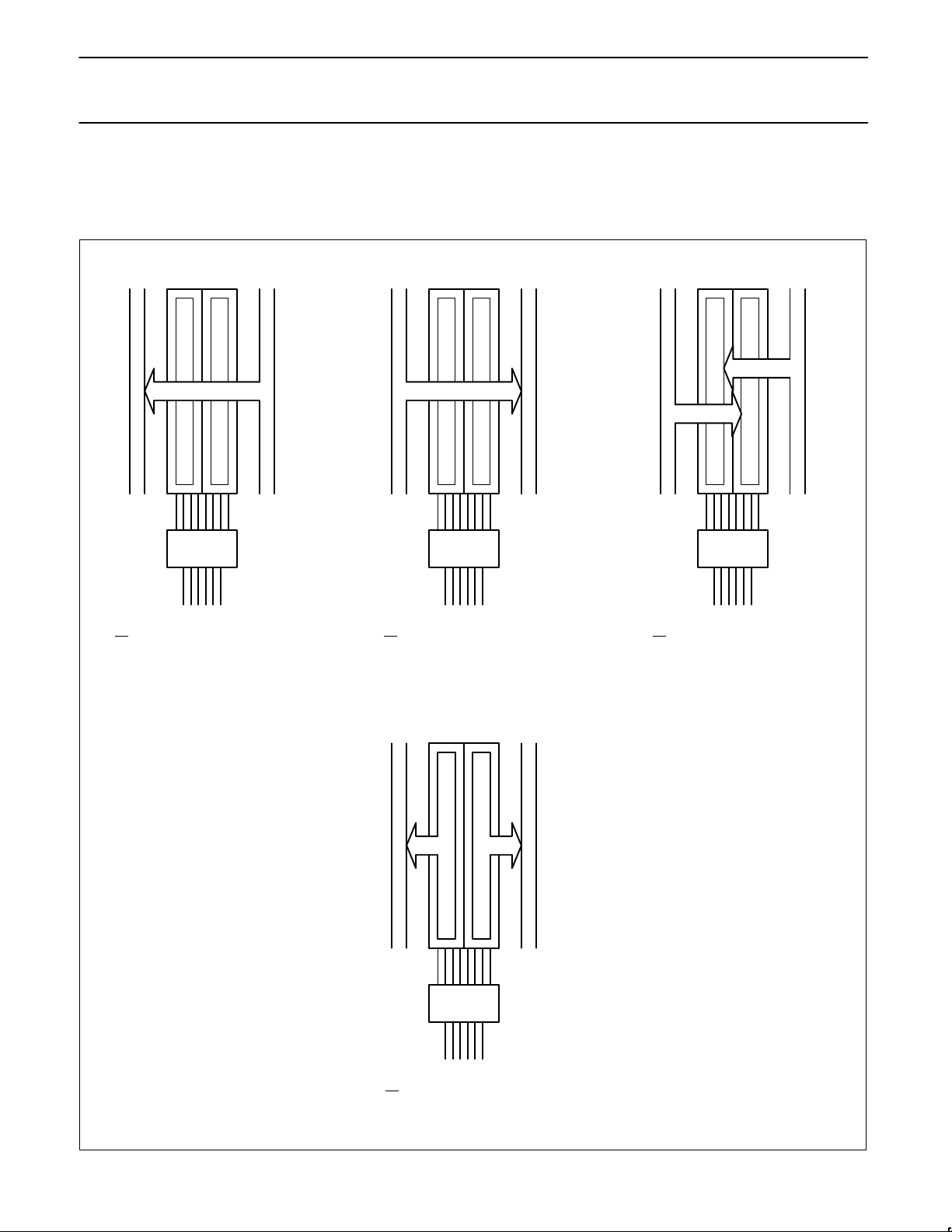
The following examples demonstrate the four
fundamental bus-management functions that
can be performed with the MB2646.
}
REAL TIME BUS TRANSFER
BUS B TO BUS A
nOE nDIR nCPAB nCPBA nSAB nSBA
L L X X X L
}
REAL TIME BUS TRANSFER
BUS A TO BUS B
nOE nDIR nCPAB nCPBA nSAB nSBA
L H X X L X
}
STORAGE FROM
A, B, OR A AND B
nOE nDIR nCPAB nCPBA nSAB nSBA
L H ↑ X X X
L L X ↑ X X
H X ↑ ↑ X X
}
TRANSFER STORED DATA
TO A OR B
nOE nDIR nCPAB nCPBA nSAB nSBA
L L X H | L X H
L H H | L X H X
A B A B A B
A B

Philips Semiconductors Products Product specification
MB2646
Dual octal bus transceiver/registers (3-State)
August 23, 1993
4
LOGIC DIAGRAM
1D
C1
Q
nB1
nB2
nB3
nB4
nB5
nB6
nB7
nA1
nA2
nA3
nA4
nA5
nA6
nA7
DETAIL A X 7
nOE
nDIR
nCPBA
nSBA
nCPAB
nSAB
nB0
1D
C1
Q
nA0
1of 8 Channels
FUNCTION TABLE
INPUTS DATA I/O OPERATING MODE
nOE nDIR nCPAB nCPBA nSAB nSBA nAx nBx
X X ↑ X X X Input
Unspecified
output*
Store A, B unspecified
X X X ↑ X X
Unspecified
output*
Input Store B, A unspecified
H
H
X
X
↑
H or L
↑
H or L
X
X
X
X
Input Input
Store A and B data
Isolation, hold storage
L
L
L
L
X
X
X
H or L
X
X
L
H
Output Input
Real time B data to A bus
Stored B data to A bus
L
L
H
H
X
H or L
X
X
L
H
X
X
Input Output
Real time A data to B bus
Stored A data to B bus
H = High voltage level
L = Low voltage level
X = Don’t care
↑ = Low-to-High clock transition
* The data output function may be enabled or disabled by various signals at the nOE
input. Data input functions are always enabled, i.e.,
data at the bus pins will be stored on every Low-to-High transition of the clock.
Philips Semiconductors Products Product specification
MB2646
Dual octal bus transceiver/registers (3-State)
August 23, 1993
5
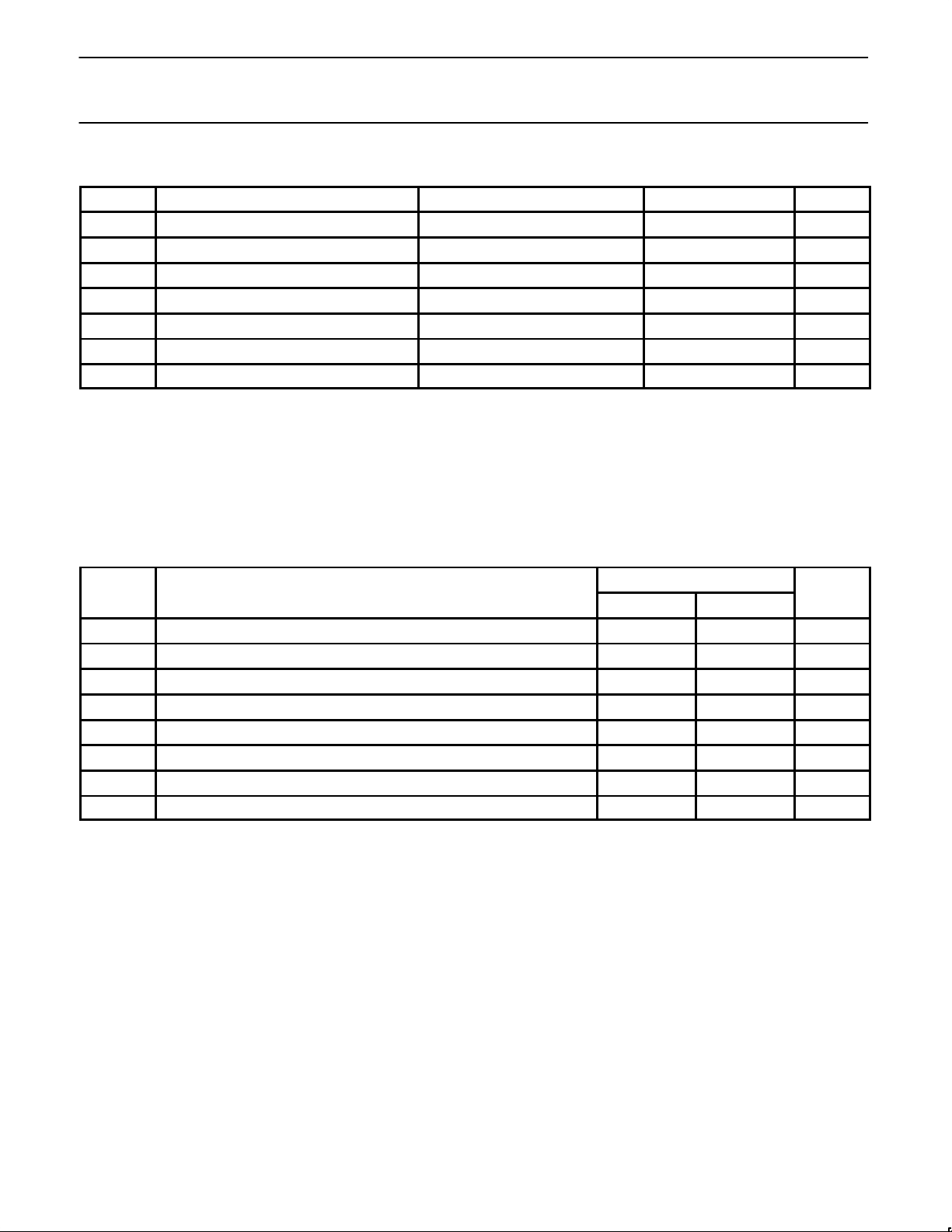
ABSOLUTE MAXIMUM RATINGS
1, 2
SYMBOL
PARAMETER CONDITIONS RATING UNIT
V
CC
DC supply voltage –0.5 to +7.0 V
I
IK
DC input diode current VI < 0 –18 mA
V
I
DC input voltage
3
–1.2 to +7.0 V
I
OK
DC output diode current VO < 0 –50 mA
V
OUT
DC output voltage
3
output in Off or High state –0.5 to +5.5 V
I
OUT
DC output current output in Low state 128 mA
T
stg
Storage temperature range –65 to 150 °C
NOTES:
1. Stresses beyond those listed may cause permanent damage to the device. These are stress ratings only and functional operation of the
device at these or any other conditions beyond those indicated under “recommended operating conditions” is not implied. Exposure to
absolute-maximum-rated conditions for extended periods may affect device reliability.
2. The performance capability of a high-performance integrated circuit in conjunction with its thermal environment can create junction
temperatures which are detrimental to reliability. The maximum junction temperature of this integrated circuit should not exceed 150°C.
3. The input and output voltage ratings may be exceeded if the input and output current ratings are observed.
RECOMMENDED OPERATING CONDITIONS
SYMBOL PARAMETER LIMITS UNIT
MIN MAX
V
CC
DC supply voltage 4.5 5.5 V
V
I
Input voltage 0 V
CC
V
V
IH
High-level input voltage 2.0 V
V
IL
Low-level Input voltage 0.8 V
I
OH
High-level output current –32 mA
I
OL
Low-level output current 64 mA
∆t/∆v Input transition rise or fall rate 0 10 ns/V
T
amb
Operating free-air temperature range –40 +85 °C
 Loading...