

Philips mb2377 DATASHEETS

Philips Semiconductors Products
Product specification
MB2377
Dual octal D-type flip-flop with enable
1
August 23, 1993 853-1666 10588
FEATURES
•Ideal for addressable register applications
•Two 8-bit positive edge-triggered registers
•Two Enable inputs for address and data
synchronization applications
•Power-up reset
•Output capability: +64mA/–32mA
•Latch-up protection exceeds 500mA per
Jedec JC40.2 Std 17
•ESD protection exceeds 2000 V per MIL
STD 883 Method 3015 and 200 V per
Machine Model
DESCRIPTION
The MB2377 high-performance BiCMOS
device combines low static and dynamic
power dissipation with high speed and high
output drive.
The MB2377 has two 8-bit, edge triggered
registers, with individual D inputs and Q
outputs. The common buffered clock (1CP or
2CP) input will load a set of eight flip-flops
simultaneously when the corresponding
Enable (1E
or 2E) input is Low.
The registers are fully edge triggered. The
state of each D input, one set-up time before
the Low-to-High clock transition, is
transferred to the corresponding flip-flop’s Q
output.
The nE
inputs must be stable one setup time
prior to the Low-to-High clock transition for
predictable operation.
QUICK REFERENCE DATA
SYMBOL PARAMETER
CONDITIONS
T
amb
= 25°C; GND = 0V
TYPICAL UNIT
t
PLH
t
PHL
Propagation delay
nCP to nQx
CL = 50pF; VCC = 5V 4.8 ns
C
IN
Input capacitance VI = 0V or V
CC
4 pF
ORDERING INFORMATION
PACKAGES TEMPERATURE RANGE ORDER CODE DRAWING NUMBER
52-pin plastic Quad Flat Pack (QFP) -40°C to +85°C MB2377BB 1418B
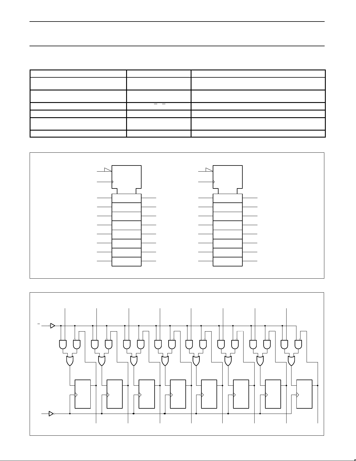
PIN CONFIGURATION LOGIC SYMBOL
4948
1Q0 1Q1 1Q2
5251
1Q3
44 43 41 40
1D0 1D1 1D2 1D3
45
47
32
1Q4 1Q5 1Q6651Q7
38 37 35 34
1D4 1D5 1D6 1D7
1CP
1E
98
2Q0 2Q1 2Q2
1211
2Q3
32 31 29 28
2D0 2D1 2D2 2D3
21
19
1514
2Q4 2Q5 2Q6
1817
2Q7
26 25 23 22
2D4 2D5 2D6 2D7
2CP
2E
1Q3
1Q2
GND
1Q1
1Q01EGND
1CP
1D0
1D1
GND
1D2
1D3
2Q4
2Q5
GND
2Q6
2Q7
2E
GND
2CP
2D7
2D6
GND
2D5
2D4
19 2220 231716 25 26241514 2118
1Q7
2Q1
GND
GND
GND
1Q5
2Q3
V
CC
2Q2
1Q4
2Q0
1Q6
V
CC
1
2
3
4
5
6
7
8
9
10
11
12
13
47 4446 434950 41 40425152 4548
1D7
2D1
GND
GND
GND
1D5
2D3
V
CC
2D2
1D4
2D0
1D6
V
CC
39
38
37
36
35
34
33
32
31
30
29
28
27
MB2377
52-pin PQFP
È
È
È
È
È
È
Philips Semiconductors Products Product specification
MB2377
Dual octal D-type flip-flop with enable
August 23, 1993
2
PIN DESCRIPTION
PIN NUMBER SYMBOL FUNCTION
44, 43, 41, 40, 38, 37, 35, 34,
32, 31, 29, 28, 26, 25, 23, 22
1D0 – 1D7
2D0 – 2D7
Data inputs
48, 49, 51, 52, 2, 3, 5, 6,
8, 9, 11, 12, 14, 15, 17, 18
1Q0 – 1Q7
2Q0 – 2Q7
Data outputs
47, 19 1E, 2E Enable inputs (active-Low)
45, 21 1CP, 2CP Clock pulse inputs (active rising edge)
4, 7, 10, 16, 20, 24, 30, 33,
36, 42, 46, 50
GND Ground (0V)
1, 13, 27, 39 V
CC
Positive supply voltage
LOGIC SYMBOL (IEEE/IEC)
45
47
44
48
43
49
41
51
40
52
G1
1C2
38
2
37
3
35
5
34
6
2D
19
32
8
31
9
29
11
28
12
G1
21
1C2
26
14
25
15
23
17
22
18
2D
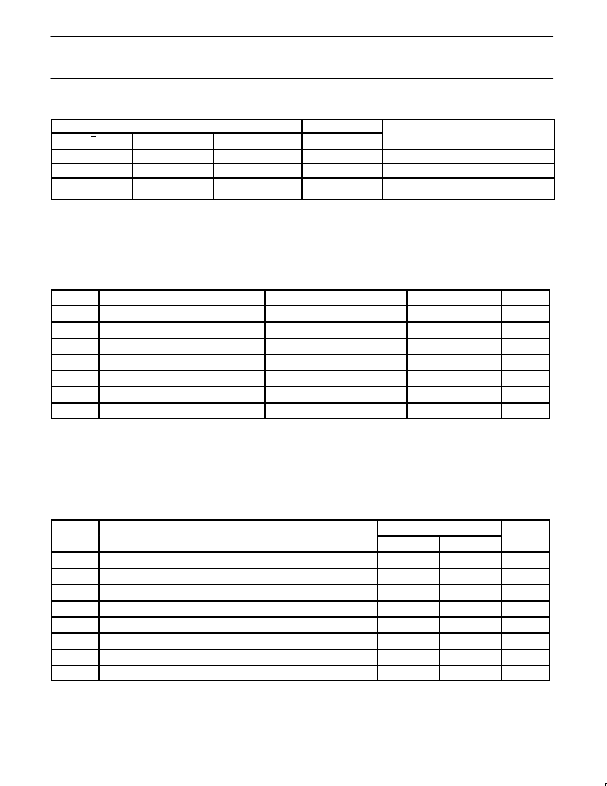
LOGIC DIAGRAM
D Q
CP
D
CP
D
CP
D Q
CP
QQ
nQ0 nQ1 nQ2 nQ3
nCP
nD0 nD1 nD2 nD3
D Q
CP
D
CP
D
CP
D Q
CP
QQ
nD4 nD5 nD6 nD7
nQ4 nQ5 nQ6 nQ7
nE
Philips Semiconductors Products Product specification
MB2377
Dual octal D-type flip-flop with enable
August 23, 1993
3
FUNCTION TABLE
INPUTS OUTPUTS OPERATING MODE
nE nCP nDx nQx
l ↑ h H Load “1”
l ↑ l L Load “0”
h
H
↑
X
X
X
no change
no change
Hold (do nothing)
H = High voltage level
h = High voltage level one set-up time prior to the Low-to-High clock transition
L = Low voltage level
l = Low voltage level one set-up time prior to the Low-to-High clock transition
X = Don’t care
↑ = Low-to-High clock transition
ABSOLUTE MAXIMUM RATINGS
1, 2
SYMBOL
PARAMETER CONDITIONS RATING UNIT
V
CC
DC supply voltage –0.5 to +7.0 V
I
IK
DC input diode current VI < 0 –18 mA
V
I
DC input voltage
3
–1.2 to +7.0 V
I
OK
DC output diode current VO < 0 –50 mA
V
OUT
DC output voltage
3
output in Off or High state –0.5 to +5.5 V
I
OUT
DC output current output in Low state 128 mA
T
stg
Storage temperature range –65 to 150 °C
NOTES:
1. Stresses beyond those listed may cause permanent damage to the device. These are stress ratings only and functional operation of the
device at these or any other conditions beyond those indicated under “recommended operating conditions” is not implied. Exposure to
absolute-maximum-rated conditions for extended periods may affect device reliability.
2. The performance capability of a high-performance integrated circuit in conjunction with its thermal environment can create junction
temperatures which are detrimental to reliability. The maximum junction temperature of this integrated circuit should not exceed 150°C.
3. The input and output voltage ratings may be exceeded if the input and output current ratings are observed.
RECOMMENDED OPERATING CONDITIONS
SYMBOL PARAMETER LIMITS UNIT
Min Max
V
CC
DC supply voltage 4.5 5.5 V
V
I
Input voltage 0 V
CC
V
V
IH
High-level input voltage 2.0 V
V
IL
Low-level Input voltage 0.8 V
I
OH
High-level output current –32 mA
I
OL
Low-level output current 64 mA
∆t/∆v Input transition rise or fall rate 0 10 ns/V
T
amb
operating free-air temperature range –40 +85 °C
 Loading...