

Philips Semiconductors Product specification
LM124/224/324/324A/
SA534/LM2902
Low power quad op amps
1
1995 Nov 27 853-0929 16050
DESCRIPTION
The LM124/SA534/LM2902 series consists of four independent,
high-gain, internally frequency-compensated operational amplifiers
designed specifically to operate from a single power supply over a
wide range of voltages.
UNIQUE FEATURES
In the linear mode, the input common-mode voltage range includes
ground and the output voltage can also swing to ground, even
though operated from only a single power supply voltage.
The unity gain crossover frequency and the input bias current are
temperature-compensated.
FEATURES
•Internally frequency-compensated for unity gain
•Large DC voltage gain: 100dB
•Wide bandwidth (unity gain): 1MHz (temperature-compensated)
•Wide power supply range Single supply: 3V
DC
to 30VDC or dual
supplies: ±1.5V
DC
to ±15V
DC
•Very low supply current drain: essentially independent of supply
voltage (1mW/op amp at +5V
DC
)
•Low input biasing current: 45nA
DC
(temperature-compensated)
•Low input offset voltage: 2mV
DC
and offset current: 5nA
DC
•Differential input voltage range equal to the power supply voltage
•Large output voltage: 0V
DC
to VCC-1.5VDC swing
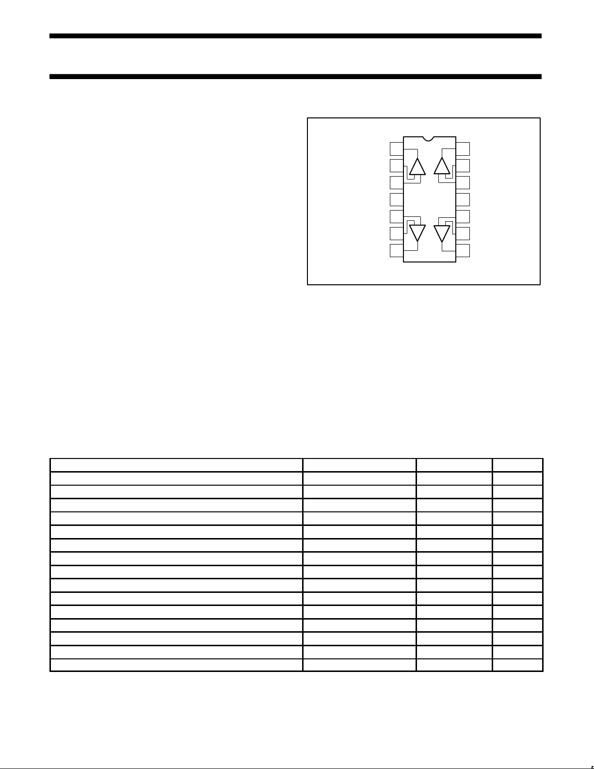
PIN CONFIGURATION
D, F, N Packages
1
2
3
4
5
6
7 8
14
13
12
11
10
9
– +
1
–+
4
– +
2
–+
3
OUTPUT 1
–INPUT 1
+INPUT 1
V +
+INPUT 2
–INPUT 2
OUTPUT 2
OUTPUT 4
–INPUT 4
+INPUT 4
GND
+INPUT 3
–INPUT 3
OUTPUT 3
TOP VIEW
SL00065
Figure 1. Pin Configuration
ORDERING INFORMATION
DESCRIPTION TEMPERATURE RANGE ORDER CODE DWG #
14-Pin Plastic Dual In-Line Package (DIP) -55°C to +125°C LM124N SOT27-1
14-Pin Ceramic Dual In-Line Package (CERDIP) -55°C to +125°C LM124F 0581B
14-Pin Plastic Dual In-Line Package (DIP) -25°C to +85°C LM224N SOT27-1
14-Pin Ceramic Dual In-Line Package (CERDIP) -25°C to +85°C LM224F 0581B
14-Pin Plastic Small Outline (SO) Package -25°C to +85°C LM224D SOT108-1
14-Pin Plastic Dual In-Line Package (DIP) 0°C to +70°C LM324N SOT27-1
14-Pin Ceramic Dual In-Line Package (CERDIP) 0°C to +70°C LM324F 0581B
14-Pin Plastic Small Outline (SO) Package 0°C to +70°C LM324D SOT108-1
14-Pin Plastic Dual In-Line Package (DIP) 0°C to +70°C LM324AN SOT27-1
14-Pin Plastic Small Outline (SO) Package 0°C to +70°C LM324AD SOT108-1
14-Pin Plastic Dual In-Line Package (DIP) -40°C to +85°C SA534N SOT27-1
14-Pin Ceramic Dual In-Line Package (CERDIP) -40°C to +85°C SA534F 0581B
14-Pin Plastic Small Outline (SO) Package -40°C to +85°C SA534D SOT108-1
14-Pin Plastic Small Outline (SO) Package -40°C to +125°C LM2902D SOT108-1
14-Pin Plastic Dual In-Line Package (DIP) -40°C to +125°C LM2902N SOT27-1
现货库存、技术资料、百科信息、热点资讯,精彩尽在鼎好!
Philips Semiconductors Product specification
LM124/224/324/324A/
SA534/LM2902
Low power quad op amps
1995 Nov 27
2
ABSOLUTE MAXIMUM RATINGS
SYMBOL PARAMETER RATING UNIT
V
CC
Supply voltage 32 or ±16 V
DC
V
IN
Differential input voltage 32 V
DC
V
IN
Input voltage -0.3 to +32 V
DC
P
D
Maximum power dissipation,
T
A
=25°C (still-air)
1
N package 1420 mW
F package 1190 mW
D package 1040 mW
Output short-circuit to GND one amplifier
2
VCC<15VDC and TA=25°C
Continuous
I
IN
Input current (VIN<-0.3V)
3
50 mA
T
A
Operating ambient temperature range
LM324/A 0 to +70 °C
LM224 -25 to +85 °C
SA534 -40 to +85 °C
LM2902 -40 to +125 °C
LM124 -55 to +125 °C
T
STG
Storage temperature range -65 to +150 °C
T
SOLD
Lead soldering temperature (10sec max) 300 °C
NOTES:
1. Derate above 25°C
at the following rates:
F package at 9.5mW/°C
N package at 11.4mW/°C
D package at 8.3mW/°C
2. Short-circuits from the output to V
CC
+ can cause excessive heating and eventual destruction. The maximum output current is approximately
40mA, independent of the magnitude of VCC. At values of supply voltage in excess of +15VDC continuous short-circuits can exceed the
power dissipation ratings and cause eventual destruction.
3. This input current will only exist when the voltage at any of the input leads is driven negative. It is due to the collector-base junction of the
input PNP transistors becoming forward biased and thereby acting as input bias clamps. In addition, there is also lateral NPN parasitic
transistor action on the IC chip. This action can cause the output voltages of the op amps to go to the V+ rail (or to ground for a large
overdrive) during the time that the input is driven negative.
Philips Semiconductors Product specification
LM124/224/324/324A/
SA534/LM2902
Low power quad op amps
1995 Nov 27
3
DC ELECTRICAL CHARACTERISTICS
VCC=5V, TA=25°C unless otherwise specified.
LM124/LM224 LM324/SA534/LM2902
SYMBOL
PARAMETER
TEST CONDITIONS
Min Typ Max Min Typ Max
UNIT
RS=0Ω ±2 ±5 ±2 ±7
VOSOffset voltage
1
RS=0Ω, over temp. ±7 ±9
mV
∆VOS/∆T Temperature drift RS=0Ω, over temp. 7 7 µV/°C
IIN(+) or IIN(-) 45 150 45 250
I
BIAS
Input current
2
IIN(+) or IIN(-), over temp. 40 300 40 500
nA
∆I
BIAS
/∆T Temperature drift Over temp. 50 50 pA/°C
IIN(+)-IIN(-) ±3 ±30 ±5 ±50
IOSOffset current
IIN(+)-IIN(-), over temp. ±100 ±150
nA
∆IOS/∆T Temperature drift Over temp. 10 10 pA/°C
VCC≤30V 0 VCC-1.5 0 VCC-1.5
V
CM
VCC≤30V, over temp. 0 VCC-2 0 VCC-2
V
CMRR
Common-mode rejection
ratio
VCC=30V 70 85 65 70 dB
V
OUT
Output voltage swing
RL=2kΩ, VCC=30V,
over temp.
26 26 V
V
OH
Output voltage high
RL≤10kΩ, VCC=30V,
over temp.
27 28 27 28 V
V
OL
Output voltage low
RL≤10kΩ,
over temp.
5 20 5 20 mV
RL=∞, VCC=30V,
over temp.
1.5 3 1.5 3
ICCSupply current
RL=∞,
over temp.
0.7 1.2 0.7 1.2
mA
VCC=15V (for large V
O
swing), RL≥2kΩ
50 100 25 100
VCC=15V (for large V
O
swing), RL≥2kΩ,
over temp.
25 15
Amplifier-to-amplifier
coupling
5
f=1kHz to 20kHz,
input referred
-120 -120 dB
PSRR Power supply rejection ratio RS≤0Ω 65 100 65 100 dB
Output current
source
VIN+=+1V, VIN-=0V,
V
CC
=15V
20 40 20 40
VIN+=+1V, VIN-=0V,
V
CC
=15V, over temp.
10 20 10 20
Output current
VIN-=+1V, VIN+=0V,
V
CC
=15V
10 20 10 20
mA
sink
VIN-=+1V, VIN+=0V,
V
CC
=15V, over temp.
5 8 5 8
VIN-=+1V, VIN+=0V,
V
O
=200mV
12 50 12 50 µA
I
SC
Short-circuit current
4
10 40 60 10 40 60 mA
GBW Unity gain bandwidth 1 1 MHz
SR Slew rate 0.3 0.3 V/µs
V
NOISE
Input noise voltage f=1kHz 40 40 nV/√Hz
V
DIFF
Differential input voltage
3
V
CC
V
CC
V
Common-mode voltage
3
range
A
VOL
Large-signal voltage gain
I
OUT
V/mV

Philips Semiconductors Product specification
LM124/224/324/324A/
SA534/LM2902
Low power quad op amps
1995 Nov 27
4
DC ELECTRICAL CHARACTERISTICS (Continued)
VCC=5V, TA=25°C unless otherwise specified.
LM324A
SYMBOL
PARAMETER
TEST CONDITIONS
Min Typ Max
UNIT
RS=0Ω ±2 ±3
VOSOffset voltage
1
RS=0Ω, over temp. ±5
mV
∆VOS/∆T Temperature drift RS=0Ω, over temp. 7 30 µV/°C
IIN(+) or IIN(-) 45 100
I
BIAS
Input current
2
IIN(+) or IIN(-), over temp. 40 200
nA
∆I
BIAS
/∆T Temperature drift Over temp. 50 pA/°C
IIN(+)-IIN(-) ±5 ±30
IOSOffset current
IIN(+)-IIN(-), over temp. ±75
nA
∆IOS/∆T Temperature drift Over temp. 10 300 pA/°C
V
CM
Common-mode voltage range
3
VCC≤30V 0 VCC-1.5 V
VCC≤30V, over temp. 0 VCC-2 V
CMRR Common-mode rejection ratio VCC=30V 65 85 dB
V
OUT
Output voltage swing
RL=2kΩ, VCC=30V,
over temp.
26 V
V
OH
Output voltage high RL≤10kΩ, VCC=30V, over temp. 27 28 V
V
OL
Output voltage low
RL≤10kΩ,
over temp.
5 20 mV
I
CC
Supply current RL=∞, VCC=30V, over temp. 1.5 3 mA
RL=∞, over temp. 0.7 1.2 mA
A
VOL
Large-signal voltage gain VCC=15V (for large VO swing), RL≥2kΩ 25 100 V/mV
VCC=15V (for large VO swing), RL≥2kΩ,
over temp.
15 V/mV
Amplifier-to-amplifier coupling
5
f=1kHz to 20kHz,
input referred
-120 dB
PSRR Power supply rejection ratio RS≤0Ω 65 100 dB
Output current
source
VIN+=+1V, VIN-=0V, VCC=15V 20 40 mA
VIN+=+1V, VIN-=0V, VCC=15V, over temp. 10 20 mA
I
OUT
Output current VIN-=+1V, VIN+=0V
,
VCC=15V 10 20 mA
sink VIN-=+1V, VIN+=0V, VCC=15V, over temp. 5 8 mA
VIN-=+1V, VIN+=0V, VO=200mV 12 50 µA
I
SC
Short-circuit current
4
10 40 60 mA
V
DIFF
Differential input voltage
3
V
CC
V
GBW Unity gain bandwidth 1 MHz
SR Slew rate 0.3 V/µs
V
NOISE
Input noise voltage f=1kHz 40 nV/√Hz
NOTES:
1. V
O
≈ 1.4VDC, RS=0Ω with VCC from 5V to 30V and over full input common-mode range (0VDC+ to VCC -1.5V).
2. The direction of the input current is out of the IC due to the PNP input stage. This current is essentially constant, independent of the state of
the output so no loading change exists on the input lines.
3. The input common-mode voltage or either input signal voltage should not be allowed to go negative by more than 0.3V . The upper end of the
common-mode voltage range is V
CC
-1.5, but either or both inputs can go to +32V without damage.
4. Short-circuits from the output to V
CC
can cause excessive heating and eventual destruction. The maximum output current is approximately
40mA independent of the magnitude of VCC. At values of supply voltage in excess of +15VDC, continuous short-circuits can exceed the
power dissipation ratings and cause eventual destruction. Destructive dissipation can result from simultaneous shorts on all amplifiers.
5. Due to proximity of external components, insure that coupling is not originating via stray capacitance between these external parts. This
typically can be detected as this type of coupling increases at higher frequencies.

Philips Semiconductors Product specification
LM124/224/324/324A/
SA534/LM2902
Low power quad op amps
1995 Nov 27
5
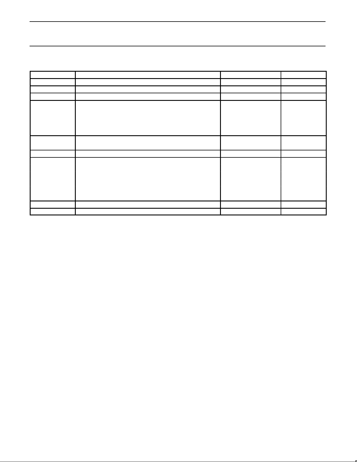
EQUIVALENT CIRCUIT
v
+
6
µ
A
100µ
A
Q2 Q3
Q1 Q4
INPUTS
+
Q8 Q9
C
C
Q10
6µ
A
Q5
Q7
Q6
R
SC
OUTPUT
Q13
Q12
Q11
50µA
SL00066
Figure 2. Equivalent Circuit

Philips Semiconductors Product specification
LM124/224/324/324A/
SA534/LM2902
Low power quad op amps
1995 Nov 27
6
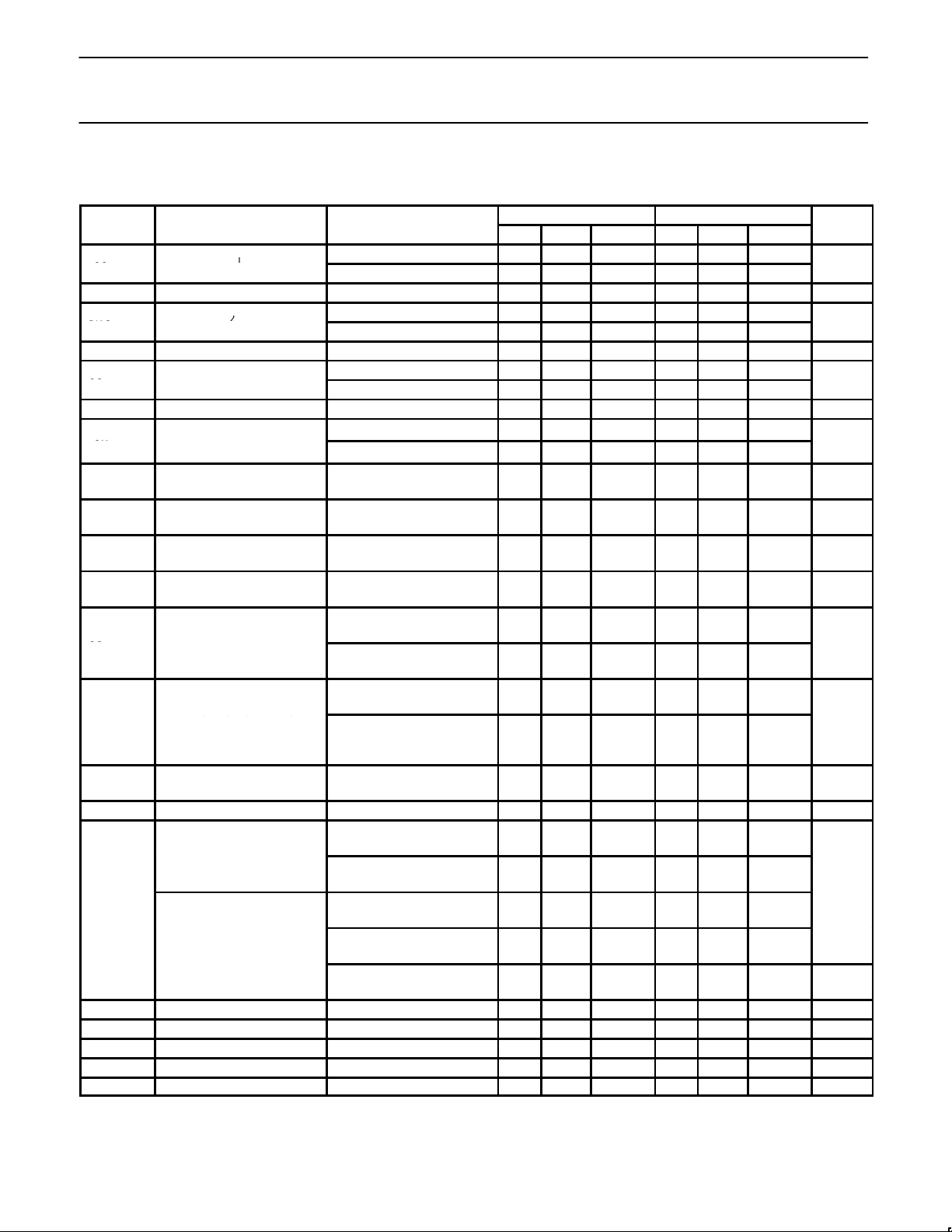
TYPICAL PERFORMANCE CHARACTERISTICS
OP05450S
OP05460S OP05470S
OP05480S
OP05490S
OP05500S
SUPPLY CURRENT DRAIN (mAdc)
TA = 0oC to +125oC
TA = -55oC
4
3
2
1
0
0
10
20 30 40
SUPPLY VOLTAGE (VDC)
V – OUTPUT VOLTAGE
REFERENCE TO V+ (V )
DC
∆
+V
+
/2
V+
V
2
I
O
INDEPENDENT OF V+
T
A
= +25oC
8
7
6
5
4
3
2
1
0.001 0.01 0.1 1 10 100
I
O
+
– OUTPUT SOURCE CURRENT (mADC)
+
–
OUTPUT CURRENT (mAdc)
90
80
70
60
50
40
30
20
10
0
55 35 –15 5 25 45 65 85 105 125
TEMPERATURE (
o
C)
A — VOLTAGE GAIN (dB)
VOL
VOLTAGE GAIN (dB)
–
+
V
+
10M
V
O
0.1µf
V
+
/2
V
IN
V+ = 30 VDC AND
–55oC < TA < +125oC
V+ = 10 to 15 VDC AND
–55oC < TA < +125oC
140
120
100
80
60
40
20
0
1 10 100 1K 10K 100K 1M 10M
FREQUENCY (Hz)
160
120
80
40
0
0 10 20 30 40
SUPPLY VOLTAGE (V
DC
)
RL + 20 KΩ
RL + 2 KΩ
V – OUTPUT VOLTAGE (V )
O
DC
V
+
/2
V
+
I
O
TA = +25oC
V+ = +5 V
DC
V+ = +15 V
DC
V+ = +30 V
DC
10
1
0.1
0.01
0.001 0.01 0.1 1 10 100
I
O
– OUTPUT SINK CURRENT (mADC)
V
O
–
+
Supply Current
Output Characteristics
Current Sourcing
Current Limiting
Voltage Gain
Output Characteristics
Current Sinking
Open–Loop Frequency
Response
SL00067
Figure 3. Typical Performance Characteristics

Philips Semiconductors Product specification
LM124/224/324/324A/
SA534/LM2902
Low power quad op amps
1995 Nov 27
7
TYPICAL PERFORMANCE CHARACTERISTICS (Continued)
E – OUTPUT VOLTAGE (mV)
O
E
O
50pF
INPUT
OUTPUT
500
450
400
350
300
250
0 1 2 3 4 5 6 7 8
L — TIME (µS)
TA = +25oC
V
+
= +30 V
DC
I – INPUT CURRENT (nA )
B DC
VCM = 0 V
DC
V+ = +30 V
DC
V+ = +15 V
DC
V+ = +5 V
DC
90
80
70
60
50
40
30
20
10
0
–55 –35 –15 5 25 45 65 85 105 125
T
A
— TEMPERATURE (Co)
Input Current
V — OUTPUT SWING (Vp–p)
O
OUTPUT VOLTAGE (V)
INPOUT VOLTAGE (V)
–
+
V
DC
100K
V
O
1K
+
7V
DC
V
IN
2K
20
15
10
5
0
1K 10K 100K 1M
FREQUENCY (Hz)
RL < 2K V
+ =
15 V
DC
4
3
2
1
0
3
2
1
0
0 10 20 30 40
TIME (µS)
+V — INPUT VOLTAGE ( V )
IN DC
+
15
10
5
NEGATIVE
POSITIVE
0 5 10 15
— POWER SUPPLY VOLTAGE (+
VDC)
V
+
OR V–
Input Voltage Range
Large-Scale
Frequency Response
Voltage-Follower
Pulse Response
Voltage-Follower Pulse
Response (Small–Signal)
CMRR — COMMON–MODE REJECTION RATIO (dB)
100
100
100k
7.5 V
DC
V
O
100k
–
+
+
V
IN
+7.5 V
DC
120
100
80
60
40
20
0
100
1k 10k 100k
1M
f — FREQUENCY (Hz)
Common-Mode Rejection Ratio
V
IN
SL00068
Figure 4. Typical Performance Characteristics (cont.)
TYPICAL APPLICATIONS
+
V+
8
V
O
V
IN
–
+
4
V+
10K
10k
RF
BLOCKS
DC.
GAIN
R
1
RF
V+
8
RL
V
O
R
IN
V
IN
–
+
4
V+
2
V+
8
V
O
V
IN
–
4
V+
10K
10k
Single Supply Inverting Amplifier Non–Inverting Amplifier Input Biasing Voltage–Follower
V+
2
+
SL00069
Figure 5. Typical Applications
 Loading...