

Philips NE532D, NE532N, SA532D, LM2904D, LM2904DP User Manual
...
查询LM158FE供应商
INTEGRATED CIRCUITS
NE/SA/SE532
LM258/358/A/2904
Low power dual operational amplifiers
Product data
Supersedes data of 2002 Jan 22
2002 Jul 12
Philips Semiconductors Product data
Low power dual operational amplifiers
DESCRIPTION
The 532/358/LM2904 consists of two independent, high gain,
internally frequency-compensated operational amplifiers internally
frequency-compensated operational amplifiers designed specifically
to operate from a single power supply over a wide range of voltages.
Operation from dual power supplies is also possible, and the low
power supply current drain is independent of the magnitude of the
power supply voltage.
UNIQUE FEATURES
In the linear mode the input common-mode voltage range includes
ground and the output voltage can also swing to includes ground
and the output voltage can also swing to ground, even though
operated from only a single power supply voltage. The unity gain
cross frequency is temperature-compensated. The input bias current
is also temperature-compensated.
FEA TURES
•Internally frequency-compensated for unity gain
•Large DC voltage gain: 100 dB
•Wide bandwidth (unity gain): 1 MHz (temperature-compensated)
•Wide power supply range single supply: 3 V
or dual supplies: ±1.5 V
to ±15 V
DC
DC
•Very low supply current drain (400 µA)—essentially independent
of supply voltage (1 mW/op amp at +5 V
•Low input biasing current: 45 nA
•Low input offset voltage: 2 mV
temperature-compensated
DC
, and offset current: 5nA
DC
•Differential input voltage range equal to the power supply voltage
•Large output voltage: 0 V
to V+ 1.5 VDC swing
DC
DC
)
to 30 VDC,
DC
DC
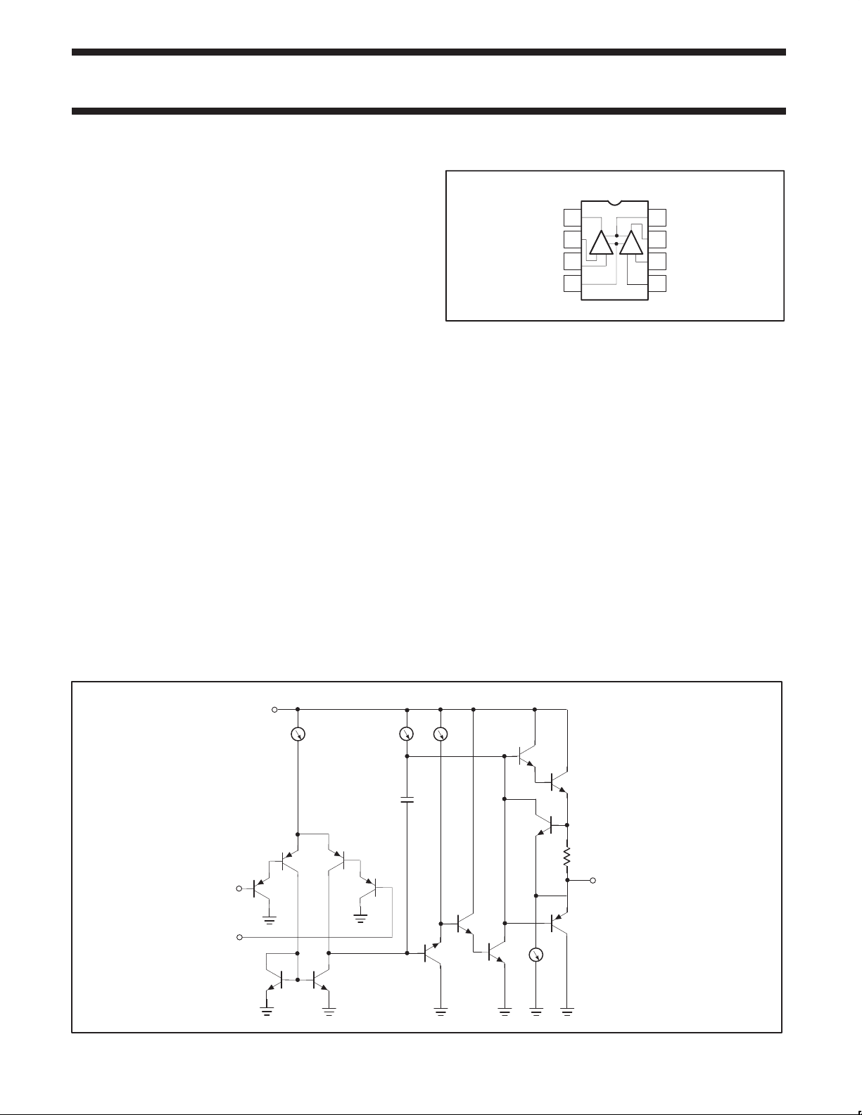
PIN CONFIGURATION
D, DP, and N Packages
OUTPUT A
INVERTING INPUT A
NON INVERTING INPUT A
1
2
3
V–
45
Figure 1. Pin configuration.
NE/SA/SE532/
LM258/358/A/2904
8
V+
7
AB
–+
+
OUTPUT B
–
6
INVERTING INPUT B
NON INVERTING INPUT B
SL00282
EQUIVALENT CIRCUIT
INPUTS
V+
Q1 Q4
–
+
Q8 Q9
6 µA 100 µ
Q2 Q3
A
6 µ
A
C
C
Q11
Q10
Figure 2. Equivalent circuit.
Q12
Q5
Q7
50 µA
Q6
Q13
R
SC
OUTPUT
SL00283
2002 Jul 12 853-1241 28616
2

Philips Semiconductors Product data
T
b
Low power dual operational amplifiers
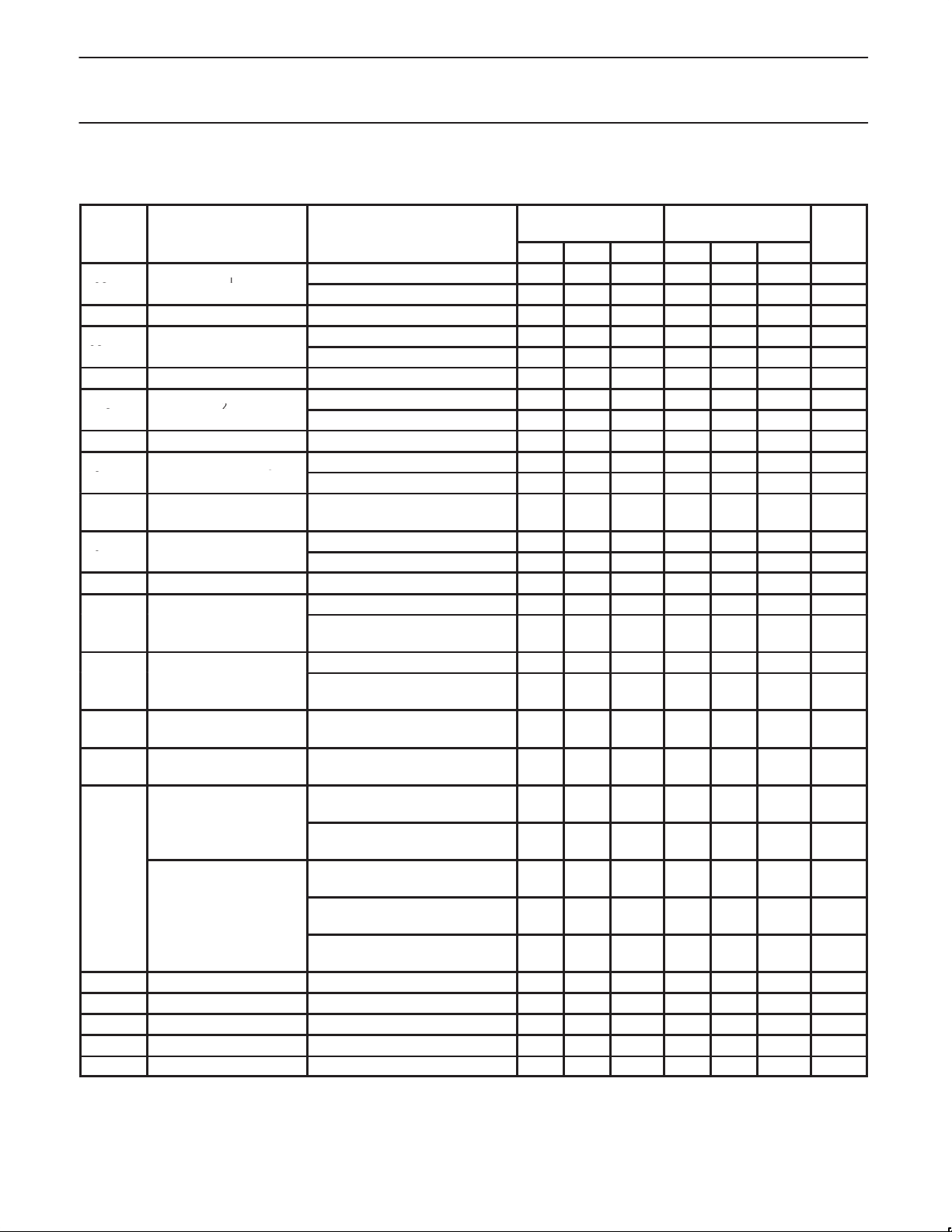
ORDERING INFORMATION
DESCRIPTION TEMPERATURE RANGE ORDER CODE DWG #
8-Pin Plastic Small Outline (SO) Package 0 °C to +70 °C NE532D SOT96-1
8-Pin Plastic Dual In-Line Package (DIP) 0 °C to +70 °C NE532N SOT97-1
8-Pin Plastic Small Outline (SO) Package –40 °C to +85 °C SA532D SOT96-1
8-Pin Plastic Small Outline (SO) Package –40 °C to +125 °C LM2904D SOT96-1
8-Pin Plastic Thin Shrink Small Outline Package (TSSOP) –40 °C to +125 °C LM2904DP SOT505-1
8-Pin Plastic Dual In-Line Package (DIP) –40 °C to +125 °C LM2904N SOT97-1
8-Pin Plastic Small Outline (SO) Package –25 °C to +125 °C LM258D SOT96-1
8-Pin Plastic Dual In-Line Package (DIP) –25 °C to +125 °C LM258N SOT97-1
8-Pin Plastic Small Outline (SO) Package 0 °C to +70 °C LM358D SOT96-1
8-Pin Plastic Thin Shrink Small Outline Package (TSSOP) 0 °C to +70 °C LM358DP SOT505-1
8-Pin Plastic Dual In-Line Package (DIP) 0 °C to +70 °C LM358N SOT97-1
8-Pin Plastic Small Outline (SO) Package 0 °C to +70 °C LM358AD SOT96-1
8-Pin Plastic Dual In-Line Package (DIP) 0 °C to +70 °C LM358AN SOT97-1
8-Pin Plastic Dual In-Line Package (DIP) –55 °C to +125 °C SE532N SOT97-1
LM258/358/A/2904
NE/SA/SE532/
ABSOLUTE MAXIMUM RATINGS
SYMBOL PARAMETER RATING UNIT
V
S
V
IN
P
D
am
T
stg
T
sld
NOTE:
1. Derate above 25 °C, at the following rates:
N package at 9.3 mW/°C
D package at 6.2 mW/°C
DP package at 5.72 mW/°C
2. Short-circuits from the output to V+ can cause excessive heating and eventual destruction. The maximum output current is approximately
40 mA independent of the magnitude of V+. At values of supply voltage in excess of +15 V
power dissipation ratings and cause eventual destruction.
Supply voltage, V+ 32 or ±16 V
Differential input voltage 32 V
Input voltage –0.3 to +32 V
Maximum power dissipation
T
= 25 °C (Still air)
amb
1
N package 1160 mW
D package 780 mW
DP package 714 mW
Output short-circuit to GND
V+ < 15 VDC and T
2
= 25 °C Continuous
amb
Operating ambient temperature range
NE532/LM358/LM358A 0 to +70 °C
LM258 –25 to +85 °C
LM2904 –40 to +125 °C
SA532 –40 to +85 °C
SE532 –55 to +125 °C
Storage temperature range –65 to +150 °C
Lead soldering temperature (10 sec max) 230 °C
, continuous short-circuits can exceed the
DC
DC
DC
DC
2002 Jul 12
3
Philips Semiconductors Product data
VOSOffset voltage
1
IOSOffset current
I
Input current
2
V
g
VOHOutput voltage swing
Output current (Source)
Low power dual operational amplifiers
DC ELECTRICAL CHARACTERISTICS
T
= 25 °C; V+ = +5 V, unless otherwise specified.
amb
SYMBOL
V
OS
I
OS
BIAS
I
B
CM
CMRR
V
OL
I
CC
A
VOL
PSRR
I
OUT
I
SC
GBW Unity gain bandwidth T
SR Slew rate T
V
NOISE
(Notes on next page).
PARAMETER TEST CONDITIONS
RS = 0 Ω ±2 ±5 ±2 ±7 mV
RS = 0 Ω; over temp. ±7 ±9 mV
Drift RS = 0 Ω; over temp. 7 7 µV/°C
I
– I
IN(+)
Over temp. ±100 ±150 nA
Drift Over temp. 10 10 pA/°C
I
or I
p
I
IN(+)
IN(+)
or I
; Over temp. 40 300 40 500 nA
IN(–)
Drift Over temp. 50 50 pA/°C
Common-mode voltage
3
range
Common-mode rejection
ratio
p
RL ≥ 2 kΩ; V+ = 30 V; over temp. 26 26 V
RL ≥ 10 kΩ; V+ = 30 V; over temp. 27 28 27 28 V
V+ = 30 V 0 V+–1.5 0 V+–1.5 V
V+ = 30 V; Over temp. 0 V+–2.0 0 V+–2.0 V
V+ = 30 V 70 85 65 70 dB
Output voltage swing RL ≥ 10 kΩ; over temp. 5 20 5 20 mV
RL = ∞; V+ = 30 V 0.5 1.0 0.5 1.0 mA
Supply current
RL=∞ on all amplifiers; V+ = 30 V;
over temp.
Large-signal voltage gain
RL ≥ 2 kΩ; V
V+=15V (for large VO swing);
OUT
over temp.
Supply voltage rejection
ratio
Amplifier-to-amplifier
4
coupling
p
f = 1 kHz to 20 kHz (input referred) –120 –120 dB
V
IN+
V
IN+
V
IN–
RS = 0 Ω 65 100 65 100 dB
= +1 VDC; V
V+ = 15 V
= +1 VDC; V
V+ = 15 V
; over temp.
DC
= +1 VDC; V
V+ = 15 V
V
= +1 VDC; V
Output current (Sink)
Short circuit current
Differential input voltage
5
6
Input noise voltage T
IN–
V+ = 15 V
V
= 0 V; V
IN+
amb
; over temp.
DC
IN–
V
= 200 mV
O
= 25 °C 1 1 MHz
amb
= 25 °C 0.3 0.3 V/µs
amb
= 25 °C; f = 1 kHz 40 40 nV/√Hz
NE/SA/SE532/
LM258/358/A/2904
SE532, LM258
Min Typ Max Min Typ Max
IN(–)
IN(–)
±3 ±30 ±5 ±50 nA
45 150 45 250 nA
0.6 1.2 0.6 1.2 mA
±10 V 50 100 25 100 V/mV
25 15 V/mV
= 0 VDC;
IN–
DC
= 0 VDC;
IN–
= 0 VDC;
IN+
DC
= 0 VDC;
IN+
= +1 VDC;
20 40 20 40 mA
10 20 10 20 mA
10 20 10 20 mA
5 8 5 8 mA
12 50 12 50 µA
40 60 40 60 mA
V+ V+ V
NE/SA532/
LM358/LM2904
UNIT
2002 Jul 12
4
 Loading...