

Philips LM139, LM239, LM239A, LM339, LM339A User Manual
...
现货库存、技术资料、百科信息、热点资讯,精彩尽在鼎好!
INTEGRATED CIRCUITS
LM139/239/239A/339/339A/LM2901/MC
3302
Quad voltage comparator
Product specification 1995 Nov 27
IC11 Data Handbook
Philips Semiconductors Product specification
Quad voltage comparator
DESCRIPTION
The LM139 series consists of four independent precision voltage
comparators, with an offset voltage specification as low as 2.0mV
max for each comparator, which were designed specifically to
operate from a single power supply over a wide range of voltages.
Operation from split power supplies is also possible and the low
power supply current drain is independent of the magnitude of the
power supply voltage. These comparators also have a unique
characteristic in that the input common–mode voltage range
includes ground, even though they are operated from a single power
supply voltage.
The LM139 series was designed to directly interface with TTL and
CMOS. When operated from both plus and minus power supplies,
the LM139 series will directly interface with MOS logic where their
low power drain is a distinct advantage over standard comparators.
FEA TURES
•Wide single supply voltage range 2.0V
supplies ±1.0V
to ±18V
DC
DC
•Very low supply current drain (0.8mA) independent of supply
voltage (1.0mW/comparator at 5.0V
•Low input biasing current 25nA
•Low input offset current ±5nA and offset voltage
•Input common–mode voltage range includes ground
•Differential input voltage range equal to the power supply voltage
•Low output 250mV at 4mA saturation voltage
•Output voltage compatible with TTL, DTL, ECL, MOS and CMOS
logic systems
APPLICATIONS
•A/D converters
•Wide range VCO
•MOS clock generator
•High voltage logic gate
•Multivibrators
to 36VDC or dual
DC
)
DC
LM139/239/239A/339/339A
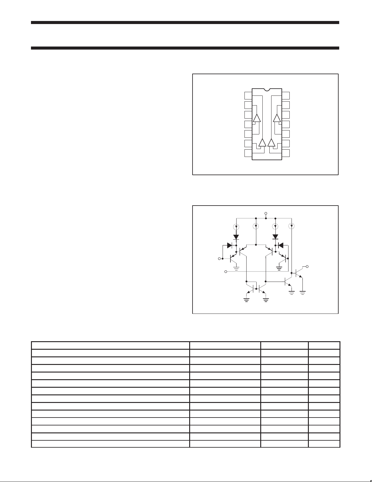
PIN CONFIGURATION
D, F, N Packages
OUTPUT 2
OUTPUT 1
INPUT 1 –
INPUT 1 +
INPUT 1 –
INPUT 1 +
EQUIVALENT CIRCUIT
+
INPUT
– INPUT
1
2
V+
3
4
5
6
78
Figure 1. Pin Configuration
Q2 Q3
Q1
(1 Comparator Only)
Figure 2. Equivalent Circuit
/LM2901/MC3302
OUTPUT 3
14
13
OUTPUT 4
GND
1
23
TOP VIEW
V
100µA3.5µA 3.5µA 100µA
Q6Q5
12
4
INPUT 4 +
11
INPUT 4 –
10
INPUT 3 +
9
INPUT 3 –
+
Q4
Q8
Q7
SL00070
OUTPUT
SL00071
ORDERING INFORMATION
DESCRIPTION TEMPERATURE RANGE ORDER CODE DWG #
14–Pin Ceramic Dual In-Line Package (Cerdip) –55 to +125°C LM139F 0581B
14–Pin Plastic Dual In-Line Package (DIP) –25°C to +85°C LM239AN SOT27-1
14–Pin Plastic Dual In-Line Package (DIP) –25°C to +85°C LM239N SOT27-1
14–Pin Plastic Small Outline (SO) Package –25°C to +85°C LM239D SOT108-1
14–Pin Plastic Dual In-Line Package (DIP) –40°C to +125°C LM2901N SOT27-1
14–Pin Plastic Small Outline (SO) Package –40°C to +125°C LM2901D SOT108-1
14–Pin Plastic Dual In-Line Package (DIP) 0 to +70°C LM339AN SOT27-1
14–Pin Plastic Small Outline (SO) Package 0 to +70°C LM339D SOT108-1
14–Pin Plastic Dual In-Line Package (DIP) 0 to +70°C LM339N SOT27-1
14–Pin Plastic Small Outline (SO) Package –40°C to +85°C MC3302D SOT108-1
14–Pin Ceramic Dual In-Line Package (Cerdip) –40°C to +85°C MC3302F 0581B
14–Pin Plastic Dual In-Line Package (DIP) –40°C to +85°C MC3302N SOT27-1
14–Pin Plastic Dual In-Line Package (DIP) –55 to +125°C LM139N SOT27-1
1995 Nov 27 853-0930 16050
2
Philips Semiconductors Product specification
Quad voltage comparator
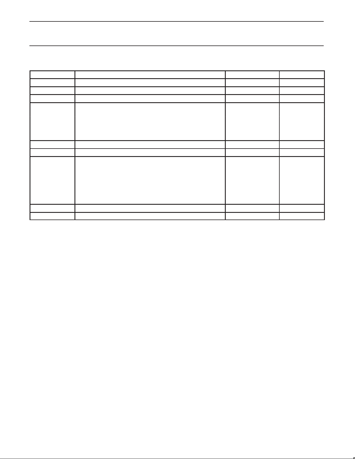
ABSOLUTE MAXIMUM RATINGS
SYMBOL PARAMETER RATING UNIT
V
CC
V
DIFF
V
IN
P
D
I
IN
T
A
T
STG
T
SOLD
NOTES:
Derate above 25°C, at the following rates:
1.
F Package at 9.5mW/°C
N Package at 11.4mW/ °C
D Package at 8.3mW/°C
2. Short circuits from the output to V+ can cause excessive heating and eventual destruction. The maximum output current is approximately
20mA independent of the magnitude of V+.
3. This input current will only exist when the voltage at any of the input leads is driven negative. It is due to the collector–base junction of the
input PNP transistors becoming forward biased and thereby acting as input diode clamps. In addition to this diode action, there is also lateral
NPN parasitic transistor action on the IC chip. This transistor action can cause the output voltages of the comparators to go to the V+ voltage
level (or to ground for a large overdrive) for the time duration that an input is driven negative. This is not destructive and normal output states
will reestablish when the input voltage, which was negative, again returns to a value greater than –0.3V
VCC supply voltage 36 or ±18 V
Differential input voltage 36 V
Input voltage –0.3 to +36 V
Maximum power dissipation,
T
=25°C (still–air)
A
1
F package 1190 mW
N package 1420 mW
D package 1040 mW
Output short–circuit to ground
Input current (VIN<–0.3VDC)
2
3
Operating temperature range
LM139 –55 to +125 °C
LM239/239A –25 to +85 °C
LM339/339A 0 to +70 °C
LM2901 –40 to +125 °C
MC3302 –40 to +85 °C
Storage temperature range –65 to +150 °C
Lead soldering temperature (10sec max) 300 °C
LM2901/MC3302
Continuous
50 mA
.
DC
DC
DC
DC
LM139/239/239A/339/339A/
1995 Nov 27
3
 Loading...