


Philips Semiconductors Linear Products Product specification
LM219/319Dual voltage comparator
277
August 31, 1994 853-0928 13721
DESCRIPTION
The LM319 series are precision high-speed dual comparators
fabricated on a single monolithic chip. They are designed to operate
over a wide range of supply voltages down to a single 5V logic
supply and ground. Further, they have higher gain and lower input
currents than devices like the µA710. The uncommitted collector of
the output stage makes the LM319 compatible with RTL, DTL, and
TTL as well as capable of driving lamps and relays at currents up to
25mA.
Although designed primarily for applications requiring operation from
digital logic supplies, the LM319 series are fully specified for power
supplies up to ±15V. It features faster response than the LM1 11 at
the expense of higher power dissipation. However, the high-speed,
wide operating voltage range and low package count make the
LM319 much more versatile than older devices like the µA711.
FEATURES
•Two independent comparators
•Operates from a single 5V supply
•Typically 80ns response time at ±15V
•Minimum fanout of 3 (each side)
PIN CONFIGURATION
1
2
3
4
5
6
7 8
14
13
12
11
10
9
NC
NC
GND 1
+ INPUT 1
– INPUT 1
V–
OUTPUT 2
NC
OUTPUT 1
V+
– INPUT 2
+ INPUT 2
GND 2
TOP VIEW
D, N Packages
NC
•Maximum input current of 1µA over temperature
•Inputs and outputs can be isolated from system ground
•High common-mode slew rate
EQUIVALENT SCHEMATIC
Q1
R1
3.5K
R2
4K
R3
4K
R6
3K
Q4
Q3
Q2
–
+
INPUTS
R4
3K
R5
3K
Q6
R8
2K
Q22
Q5
R23
4K
R2260R20
3.6K
R9
18K
R18
1.9K
Q21
Q20
Q19
R19
250
Q18
R2
900
R24
250
R25
600
TO OTHER
HALF
R7
3K
Q9
Q8
Q7
C1
18pF
R10
170
R11
13K
R12
13K
Q15
Q10
Q13
R13
600
C14
Q12
R14
2K
Q11
Q16
R15
300
R16
600
Q12
R17 3
OUTPUT
V– GND
V+
查询LM219供应商

Philips Semiconductors Linear Products Product specification
LM219/319Dual voltage comparator
August 31, 1994
278
ORDERING INFORMATION
DESCRIPTION TEMPERATURE RANGE ORDER CODE DWG #
14-Pin Plastic Small Outline (SO) Package -25 to +85°C LM219D 0175D
14-Pin Plastic Small Outline (SO) Package 0 to +70°C LM319D 0175D
14-Pin Plastic Dual In-Line Package (DIP) 0 to +70°C LM319N 0405B
ABSOLUTE MAXIMUM RATINGS
SYMBOL PARAMETER RATING UNIT
V
S
Total supply voltage 36 V
Output to negative supply voltage 36 V
Ground to negative supply voltage 25 V
Ground to positive supply voltage 18 V
Differential input voltage ±5 V
V
IN
Input voltage
1
±15 V
Maximum power dissipation, TA=25°C (still-air)
2
N package 1420 mW
D package 1040 mW
Output short-circuit duration 10 s
T
A
Operating temperature range LM219
LM319
-25 to +85
0 to +70
°C
T
STG
Storage temperature range -65 to +150 °C
T
SOLD
Lead soldering temperature (10sec max) 300 °C
NOTES:
1. For supply voltages less than ±15V, the absolute maximum rating is equal to the supply voltage.
2. Derate above 25°C, at the following rates:
N package at 11.4mW/°C
D package at 8.3mW/°C
DC ELECTRICAL CHARACTERISTICS
VS=±15V, -25°C ≤ T
A
≤ 85°C for LM219, 0°C ≤ T
A
≤ 70°C for LM319, unless otherwise specified.
LM219 LM319
SYMBOL
PARAMETER
TEST CONDITIONS
Min Typ Max Min Typ Max
UNIT
RS≤5kΩ, TA=25°C 0.7 4.0 2.0 8.0
VOSInput offset voltage
1, 2
Over temp. 7 10
mV
TA=25°C 30 75 80 200
IOSInput offset current
1, 2
Over temp. 100 300
nA
I
B
Input bias current
1
TA=25°C 150 500 250 1000 nA
Over temp. 1000 1200 nA
A
V
Voltage gain TA=25°C 8 40 8 40 V/mV
VIN≤-10mV, I
OUT
=25mA, TA=25°C,
V+≥4.5V, V-=0
0.75 1.5 0.75 1.5
VOLSaturation voltage
VIN≤-10mV, I
OUT
=3.2mA 0.3 0.6 0.3 0.4
V
I
OH
Output leakage current V-=0V, VIN≥10mV
V
OUT
=35V, TA=25°C 0.2 10 0.2 10 µA
VS=±15V ±13 ±13
VINInput voltage range
V+=5V, V-=0V 1 3 1 3
V
V
ID
Differential input voltage ±5 ±5 V
I+ Positive supply current V+=5V, V-=0V, TA=25°C 4.3 4.3 mA
I+ Positive supply current VS=±15V, TA=25°C 8.0 12.5 8.0 12.5 mA
I- Negative supply current VS=±15V, TA=25°C 3.0 5.0 3.0 5.0 mA
NOTES:
1. V
OS
, IOS and IB specifications apply for a supply voltage range of VS=±15V down to a single 5V supply.
2. The offset voltages and offset currents given are the maximum values required to drive the output to within 1V of either supply with a 1mA
load. Thus these parameters define an error band and take into account the worst case effects of voltage gain and input impedance.
V
OL
Saturation voltage
V
Philips Semiconductors Linear Products Product specification
LM219/319Dual voltage comparator
August 31, 1994
279
AC ELECTRICAL CHARACTERISTICS
LIMITS
SYMBOL
PARAMETER
TEST CONDITIONS
Min Typ Max
UNIT
t
R
Response time
1
VS=±15V, TA=25°C
R
L
=500Ω (see test figure)
80 ns
NOTES:
1. The response time specified is for a 100mV step with 5mV overdrive.
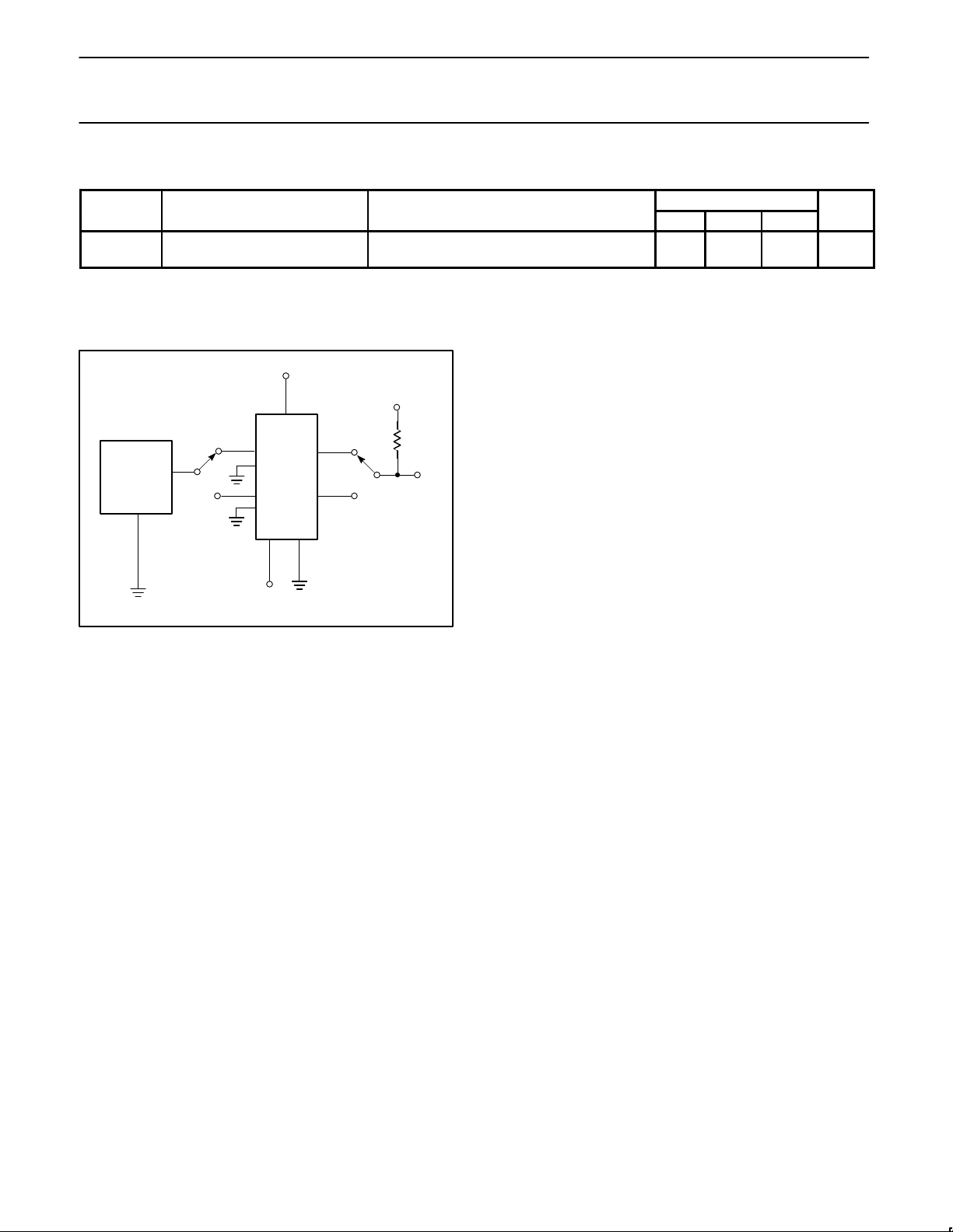
TEST CIRCUIT
PULSE
GENERATOR
D.U.T.
+15V
–15V
+5V
R
L
V
OUT
Response Time Measurement
Philips Semiconductors Linear Products Product specification
LM219/319Dual voltage comparator
August 31, 1994
280
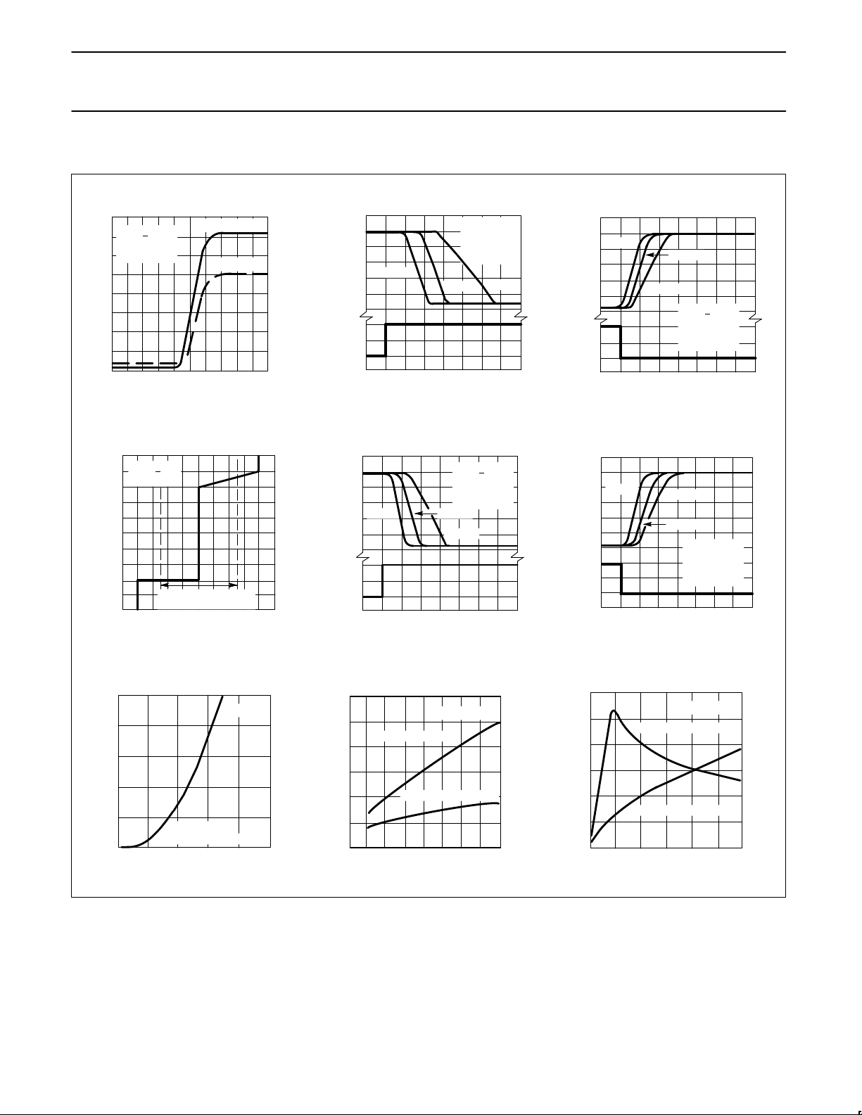
TYPICAL PERFORMANCE CHARACTERISTICS
Transfer Function
Response Time for Various
Input Overdrives
Response Time for Various
Input Overdrives
Input Characteristics
Response Time for Various
Input Overdrives
Response Time for Various
Input Overdrives
Output Saturation Voltage Supply Current
Output Limitiung
Characteristics
OUTPUT VOLTAGE HIGH – V
OUTPUT VOLTAGE LOW – V
40
35
30
25
20
15
10
5
0
-1.0 -0.6 -0.2 0.2 0.6 1.0
8.0
7.0
6.0
5.0
4.0
3.0
2.0
1.0
0
DIFFERENTIAL INPUT VOLTAGE – V
VS = +15V
R
L
= 1.4KΩ
T
A
= 25oC
V
+ +
= 36V
V
+ +
= 5.0V
INPUT
VOLTAGE – mV
OUTPUT
VOLTAGE – V
6.0
5.0
4.0
3.0
2.0
1.0
0
0
-50
-100
TIME – ns
0 50 100 150 200 250 300 350
TIME – ns
0 50 100 150 200 250 300 350
INPUT
VOLTAGE – mV
OUTPUT
VOLTAGE – V
6.0
5.0
4.0
3.0
2.0
1.0
0
100
50
0
VS = 5.0V
R
L
= 500KΩ
V
+ +
= 5.0V
TA = 25oC
20mV
5.0mV
2.0mV
VS = +15V
R
L
= 500KΩ
V
+ +
= 5.0V
T
A
= 25oC
2.0mV
5.0mV
20mV
INPUT BIAS CURRENT – nA
VS = +15V
T
A
= 25oC
400
300
200
100
0
-100
-10 -6.0 -2.0 2.0 6.0 10
DIFFERENTIAL INPUT VOLTAGE – V
VS = +15V
R
L
= 500KΩ
V
+ +
= 5.0V
T
A
= 25oC
5.0mV
2.0mV
20mV
0 50 100 150 200 250 300 350
6.0
5.0
4.0
3.0
2.0
1.0
0
0
-50
-100
TIME – ns
0 50 100 150 200 250 300 350
TIME – ns
6.0
5.0
4.0
3.0
2.0
1.0
0
100
50
0
INPUT
VOLTAGE – mV
OUTPUT
VOLTAGE – V
VS = 5.0V
R
L
= 500KΩ
V
+ +
= 5.0V
T
A
= 25oC
INPUT
VOLTAGE – mV
OUTPUT
VOLTAGE – V
20mV
5.0mV
2.0mV
OUTPUT CURRENT – mA
TA = 25oC
VS =
+
15V
INPUT OVERDRIVE = 5.0mV
0
5
10
15
20
25
0 0.2 0.4 0.6 0.8 1.0
OUTPUT VOLTAGE – V
TA = 25oC
POSITIVE SUPPLY
NEGATIVE SUPPLY
0 5 10 15 20
12
10
8
6
4
2
0
SUPPLY VOLTAGE – V
SUPPLY CURRENT – mA
SHORT CIRCUIT CURRENT – mA
POWER DISSIPATION – W
OUTPUT VOLTAGE – V
0 5 10 15
120
100
80
60
40
20
0
1.2
1.0
0.8
0.6
0.4
0.2
0
TA = 25oC
SHORT CIRCUIT CURRENT
POWER DISSIPATION
MAXIMUM DIFFERENTIAL
INPUT VOLTAGE

Philips Semiconductors Linear Products Product specification
LM219/319Dual voltage comparator
August 31, 1994
281
TYPICAL PERFORMANCE CHARACTERISTICS (Continued)
Input Currents
INPUT CURRENT – nA
TEMPERATURE – oC
VS = +15V
BIAS
OFFSET
-55 -15 5 45 85 125
250
200
150
100
50
0
Common-Mode Limits
V
S
+
= 5.0V, V
S
-
= 0
VS = +15V
REFERRED TO SUPPLY VOLTAGES
VS = +15V, V
S
+
= 5.0V, V- = 0
-55 -15 5 45 85 125
TEMPERATURE –
o
C
V
+
-0.4
-0.8
-1.2
-1.6
-2.0
1.2
0.8
0.4
V
-
COMMON MODE LIMITS – V
-55 -15 5 45 85 125
TEMPERATURE –
o
C
Supply Current
SUPPLY CURRENT – mA
12
10
8
6
4
2
0
POSITIVE SUPPLY, VS = +15V
POSITIVE SUPPLY, V
S
+
= 5.0V, V
S
-
= 0
NEGATIVE SUPPLY, VS = +15V
TYPICAL APPLICATIONS
1
/
2
LM319
1
/
2
LM319
+
-
+
-
1N914
3k
1k
-5V
500pF
1N914
1N914
1k
190
Ω
+
2.7k
+5V
500
1N914
1.2V
3k
NOTE:
Frequency adjust must be buffered for RL < 10Ω
Wide Range Variable Oscillator
SQUARE WAVE OUTPUT
1kHz to 1MHz
TRIANGLE WAVE OUTPUT
2N2222
1
/
2
LM319
+
-
5V 28V
30V
INPUTS
Relay Driver
1
/
2
LM319
+
-
1
/
2
LM319
+
-
500
5V
TTL
V
UT
V
IN
V
LT
Window Detector
NOTES:
V
OUT
= 5V for VLT < VIN < V
UT
V
OUT
= 0V for VIN < VLT or VIN > V
UT
7.5M
 Loading...