

Philips LM117, LM317A, LM317 Service Manual
LM117/LM317A/LM317
3-Terminal Adjustable Regulator
General Description
The LM117 series of adjustable 3-terminal positive voltage
regulators is capable of supplying in excess of 1.5A over a
1.2V to 37V output range. They are exceptionally easy to use
and require only two external resistors to set the output voltage. Further, both line and load regulation are better than
standard fixed regulators. Also, the LM117 is packaged in
standard transistor packages which are easily mounted and
handled.
In addition to higher performance than fixed regulators, the
LM117 series offers full overload protection available only in
IC's. Included on the chip are current limit, thermal overload
protection and safe area protection. All overload protection
circuitry remains fully functional even if the adjustment terminal is disconnected.
Normally, no capacitors are needed unless the device is situated more than 6 inches from the input filter capacitors in
which case an input bypass is needed. An optional output capacitor can be added to improve transient response. The
adjustment terminal can be bypassed to achieve very high
ripple rejection ratios which are difficult to achieve with standard 3-terminal regulators.
Besides replacing fixed regulators, the LM117 is useful in a
wide variety of other applications. Since the regulator is “floating” and sees only the input-to-output differential voltage,
supplies of several hundred volts can be regulated as long as
the maximum input to output differential is not exceeded, i.e.,
avoid short-circuiting the output.
Also, it makes an especially simple adjustable switching regulator, a programmable output regulator, or by connecting a
fixed resistor between the adjustment pin and output, the
LM117 can be used as a precision current regulator. Supplies
with electronic shutdown can be achieved by clamping the
adjustment terminal to ground which programs the output to
1.2V where most loads draw little current.
For applications requiring greater output current, see LM150
series (3A) and LM138 series (5A) data sheets. For the negative complement, see LM137 series data sheet.
Features
Guaranteed 1% output voltage tolerance (LM317A)
■
Guaranteed max. 0.01%/V line regulation (LM317A)
■
Guaranteed max. 0.3% load regulation (LM117)
■
Guaranteed 1.5A output current
■
Adjustable output down to 1.2V
■
Current limit constant with temperature
■
P+ Product Enhancement tested
■
80 dB ripple rejection
■
Output is short-circuit protected
■
LM117/LM317A/LM317 3-Terminal Adjustable Regulator
February 25, 2011
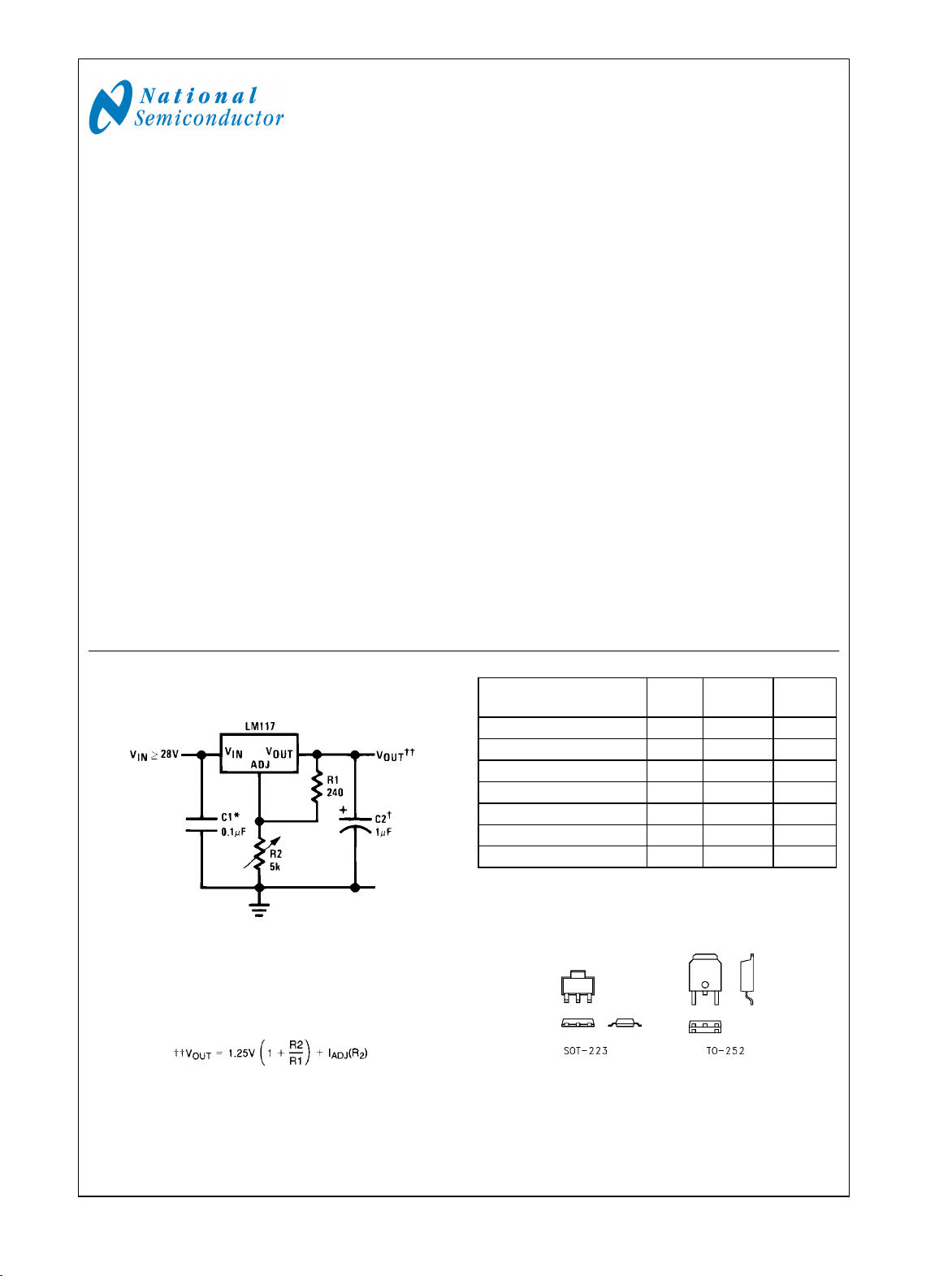
Typical Applications
1.2V–25V Adjustable Regulator
906301
Full output current not available at high input-output voltages
*Needed if device is more than 6 inches from filter capacitors.
†Optional—improves transient response. Output capacitors in the range
of 1μF to 1000μF of aluminum or tantalum electrolytic are commonly used
to provide improved output impedance and rejection of transients.
LM117/LM317A/LM317 Package Options
Part
Number
LM117, LM317 K TO-3 1.5A
LM317A, LM317 T TO-220 1.5A
LM317 S TO-263 1.5A
LM317A, LM317 EMP SOT-223 1.0A
LM117, LM317A, LM317 H TO-39 0.5A
LM117 E LCC 0.5A
LM317A, LM317 MDT TO-252 0.5A
Suffix Package
Current
SOT-223 vs. TO-252 (D-Pak) Packages
Scale 1:1
906354
Output
© 2011 National Semiconductor Corporation 9063 www.national.com
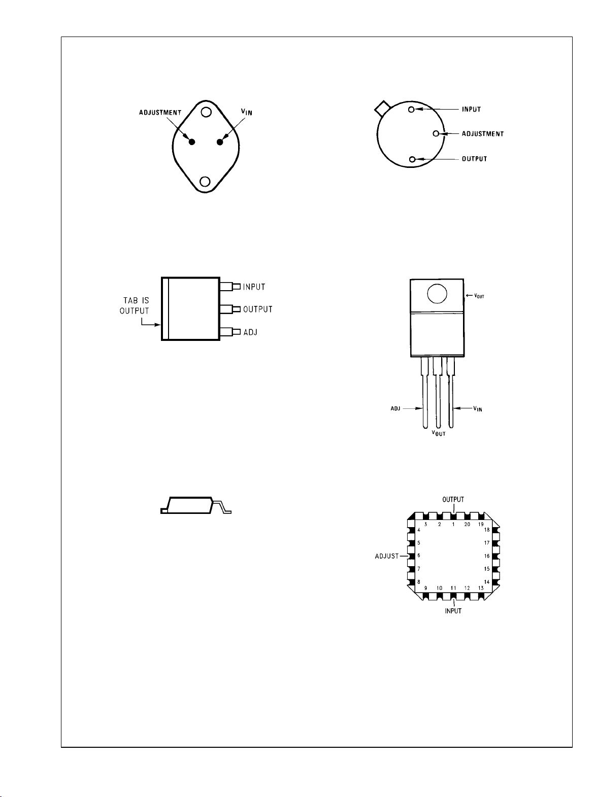
Connection Diagrams
Metal Can Package
LM117/LM317A/LM317
CASE IS OUTPUT
NS Package Number K02A or K02C
Surface-Mount Package
TO-3 (K)
Bottom View
Steel Package
TO-263 (S)
Top View
906330
TO-39 (H)
Metal Can Package
906331
CASE IS OUTPUT
Bottom View
NS Package Number H03A
TO-220 (T)
Plastic Package
906335
TO-263 (S)
Surface-Mount Package
Side View
906336
NS Package Number TS3B
Front View
906332
NS Package Number T03B
Ceramic Leadless
Chip Carrier (E)
Top View
NS Package Number E20A
906334
www.national.com 2
LM117/LM317A/LM317
4-Lead SOT-223 (EMP)
Front View
NS Package Number MP04A
Ordering Information
Package
TO-3
Metal Can
(K)
TO-220
3- Lead
TO-263
3- Lead
SOT-223
4- Lead
TO-39
Metal Can
(H)
LCC
TO-252
3- Lead
D-Pack
Temperature
Range
−55°C ≤ TJ ≤ +150°C
0°C ≤ TJ ≤ +125°C
−55°C ≤ TJ ≤ +150°C
−40°C ≤ TJ ≤ +125°C
0°C ≤ TJ ≤ +125°C
0°C ≤ TJ ≤ +125°C
0°C ≤ TJ ≤ +125°C
−40°C ≤ TJ ≤ +125°C
−55°C ≤ TJ ≤ +150°C
−55°C ≤ TJ ≤ +150°C
−40°C ≤ TJ ≤ +125°C
0°C ≤ TJ ≤ +125°C
−55°C ≤ TJ ≤ +150°C
0°C ≤ TJ ≤ +125°C
−40°C ≤ TJ ≤ +125°C
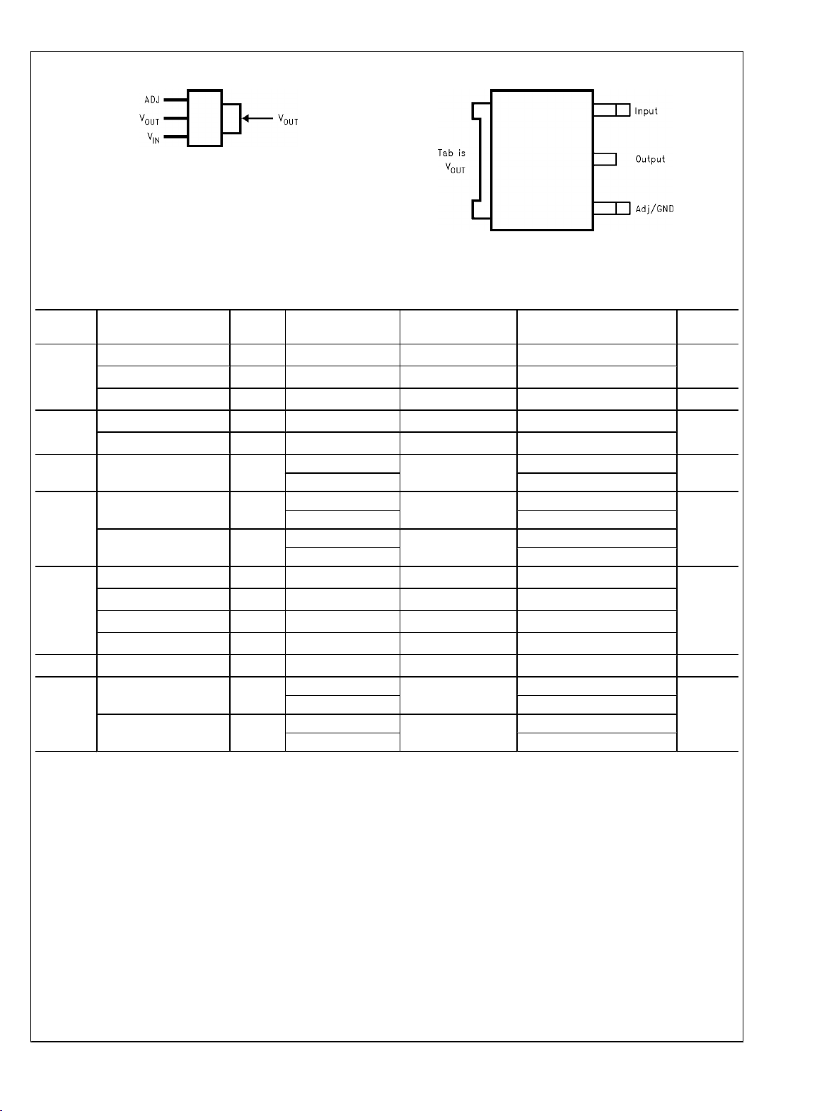
TO-252 (MDT)
906359
Front View
906366
NS Package Number TD03B
Output
Current
1.5A LM117K STEEL LM117K STEEL P+ 50 Per Bag
1.5A LM317K STEEL LM317K STEEL P+ 50 Per Bag
Order
Number
Package
Marking
Transport
Media
Drawing
K02A
1.5A LM117K/883 LM117K/883 50 Per Bag K02C
1.5A LM317AT LM317AT P+ 45 Units/Rail
1.5A LM317T LM317T P+ 45 Units/Rail
1.5A
1.0A
1.0A
LM317S
LM317SX 500 Units Tape and Reel
LM317EMP
LM317EMPX 2k Units Tape and Reel
LM317AEMP
LM317AEMPX 2k Units Tape and Reel
LM317S P+
N01A
N07A
45 Units/Rail
1k Units Tape and Reel
1k Units Tape and Reel
T03B
TS3B
MP04A
0.5A LM117H LM117H P+ 500 Per Box
0.5A LM117H/883 LM117H/883 20 Per Tray
0.5A LM317AH LM317AH P+ 500 Per Box
H03A
0.5A LM317H LM317H P+ 500 Per Box
0.5A LM117E/883 LM117E/883 50 Units/Rail E20A
0.5A
0.5A
LM317MDT
LM317MDTX 2.5k Units Tape and Reel
LM317AMDT
LM317AMDTX 2.5k Units Tape and Reel
LM317MDT
LM317AMDT
75 Units/Rail
75 Units/Rail
TD03B
NSC
3 www.national.com
Absolute Maximum Ratings (Note 1)
If Military/Aerospace specified devices are required,
please contact the National Semiconductor Sales Office/
Distributors for availability and specifications.
Power Dissipation Internally Limited
Input-Output Voltage Differential +40V, −0.3V
Storage Temperature −65°C to +150°C
Lead Temperature
LM117/LM317A/LM317
Metal Package (Soldering, 10 seconds) 300°C
Plastic Package (Soldering, 4 seconds) 260°C
ESD Tolerance (Note 5) 3 kV
Operating Temperature Range
LM117
LM317A
LM317
Preconditioning
Thermal Limit Burn-In All Devices 100%
−55°C ≤ TJ ≤ +150°C
−40°C ≤ TJ ≤ +125°C
0°C ≤ TJ ≤ +125°C
LM117 Electrical Characteristics (Note 3)
Specifications with standard type face are for TJ = 25°C, and those with boldface type apply over full Operating Temperature
Range. Unless otherwise specified, VIN − V
Parameter Conditions
Reference Voltage
Line Regulation
Load Regulation
Thermal Regulation 20 ms Pulse 0.03 0.07 %/W
Adjustment Pin Current 50 100
Adjustment Pin Current Change
Temperature Stability
Minimum Load Current
Current Limit
RMS Output Noise, % of V
OUT
Ripple Rejection Ratio
Long-Term Stability
Thermal Resistance, θ
JC
Junction-to-Case
Thermal Resistance, θ
JA
Junction-to-Ambient
(No Heat Sink)
= 5V, and I
OUT
3V ≤ (VIN − V
10 mA ≤ I
3V ≤ (VIN − V
10 mA ≤ I
10 mA ≤ I
3V ≤ (VIN − V
T
≤ TJ ≤ T
MIN
(VIN − V
OUT
(VIN − V
OUT
) ≤ 40V,
OUT
≤ I
OUT
MAX
) ≤ 40V (Note 4)
OUT
≤ I
OUT
MAX
≤ I
OUT
MAX
) ≤ 40V
OUT
MAX
) = 40V
) ≤ 15V
K Package
H, E Package
(VIN − V
OUT
) = 40V
K Package
H, E Package
10 Hz ≤ f ≤ 10 kHz
V
= 10V, f = 120 Hz, C
OUT
V
= 10V, f = 120 Hz, C
OUT
TJ = 125°C, 1000 hrs
K (TO-3) Package
H (TO-39) Package
E (LCC) Package
K (TO-3) Package
H (TO-39) Package
E (LCC) Package
= 10 mA.
OUT
(Note 3)
(Note 3, Note 4)
(Note 3)
= 0 μF
ADJ
= 10 μF
ADJ
LM117 (Note 2)
Min Typ Max Units
1.20 1.25 1.30 V
0.01
0.02
0.1
0.3
0.02
0.05
0.3
1
0.2 5
1 %
3.5 5 mA
1.5
0.5
2.2
0.8
3.4
1.8
0.3
0.15
0.4
0.20
A
0.003 %
65 dB
66 80 dB
0.3 1 %
2
21
°C/W
12
39
186
°C/W
88
%/V
%
μA
μA
A
www.national.com 4
LM317A and LM317 Electrical Characteristics (Note 3)
Specifications with standard type face are for TJ = 25°C, and those with boldface type apply over full Operating Temperature
Range. Unless otherwise specified, VIN − V
Parameter Conditions
1.238 1.250 1.262 - 1.25 - V
Reference Voltage
3V ≤ (VIN − V
10 mA ≤ I
Line Regulation
Load Regulation
3V ≤ (VIN − V
10 mA ≤ I
Thermal Regulation 20 ms Pulse 0.04 0.07 0.04 0.07 %/W
Adjustment Pin Current 50 100 50 100
Adjustment Pin Current Change
Temperature Stability
Minimum Load Current
10 mA ≤ I
3V ≤ (VIN − V
T
MIN
(VIN − V
(VIN − V
K, S Packages
EMP, T Packages
Current Limit
H, MDT Packages
(VIN − V
K, S Packages
EMP, T Packages
H, MDT Packages
RMS Output Noise, % of V
Ripple Rejection Ratio
Long-Term Stability
OUT
10 Hz ≤ f ≤ 10 kHz
V
OUT
V
OUT
TJ = 125°C, 1000 hrs
K (TO-3) Package
T (TO-220) Package
Thermal Resistance, θ
Junction-to-Case
JC
S (TO-263) Package
EMP (SOT-223) Package
H (TO-39) Package
MDT (TO-252) Package
K (TO-3) Package
Thermal Resistance, θ
Junction-to-Ambient
(No Heat Sink)
JA
T (TO-220) Package
S (TO-263) Package (Note 6)
EMP (SOT-223) Package (Note 6)
H (TO-39) Package
MDT (TO-252) Package (Note 6)
= 5V, and I
OUT
) ≤ 40V,
OUT
≤ I
OUT
OUT
OUT
≤ TJ ≤ T
) = 40V
OUT
) ≤ 15V
OUT
) = 40V
OUT
(Note 3)
MAX
) ≤ 40V (Note 4)
OUT
≤ I
(Note 3, Note 4)
MAX
≤ I
(Note 3)
MAX
) ≤ 40V
OUT
MAX
= 10V, f = 120 Hz, C
= 10V, f = 120 Hz, C
= 10 mA.
OUT
ADJ
ADJ
= 0 μF
= 10 μF
LM317A LM317
Min Typ Max Min Typ Max Units
1.225 1.250 1.270 1.20 1.25 1.30 V
0.005
0.01
0.1
0.3
0.01
0.02
0.5
1
0.01
0.02
0.1
0.3
0.04
0.07
0.5
1.5
%/V
μA
0.2 5 0.2 5
μA
1 1 %
3.5 10 3.5 10 mA
-
1.5
0.5
2.2
0.8
-
3.4
1.8
-
1.5
1.5
0.5
2.2
2.2
0.8
3.4
3.4
1.8
-
0.112
0.075
-
0.30
0.20
0.15
0.112
0.075
0.40
0.30
0.20
A
0.003 0.003 %
65 65 dB
66 80 66 80 dB
0.3 1 0.3 1 %
-
4
-
23.5
21
12
-
50
140
186
103
2
4
4
23.5
21
12
39
50
50
140
186
103
°C/W
°C/W
%
A
LM117/LM317A/LM317
Note 1: Absolute Maximum Ratings indicate limits beyond which damage to the device may occur. Operating Ratings indicate conditions for which the device is
intended to be functional, but do not guarantee specific performance limits. For guaranteed specifications and test conditions, see the Electrical Characteristics.
The guaranteed specifications apply only for the test conditions listed.
Note 2: Refer to RETS117H drawing for the LM117H, or the RETS117K for the LM117K military specifications.
Note 3: I
(TO-252), and E (LCC) packages. Device power dissipation (PD) is limited by ambient temperature (TA), device maximum junction temperature (TJ), and package
thermal resistance (θJA). The maximum allowable power dissipation at any temperature is : P
to National's Average Outgoing Quality Level (AOQL).
Note 4: Regulation is measured at a constant junction temperature, using pulse testing with a low duty cycle. Changes in output voltage due to heating effects
are covered under the specifications for thermal regulation.
Note 5: Human body model, 100 pF discharged through a 1.5 kΩ resistor.
Note 6: When surface mount packages are used (TO-263, SOT-223, TO-252), the junction to ambient thermal resistance can be reduced by increasing the PC
board copper area that is thermally connected to the package. See the Applications Hints section for heatsink techniques.
= 1.5A for the K (TO-3), T (TO-220), and S (TO-263) packages. I
MAX
= 1.0A for the EMP (SOT-223) package. I
MAX
= ((T
D(MAX)
5 www.national.com
- TA)/θJA). All Min. and Max. limits are guaranteed
J(MAX)
= 0.5A for the H (TO-39), MDT
MAX
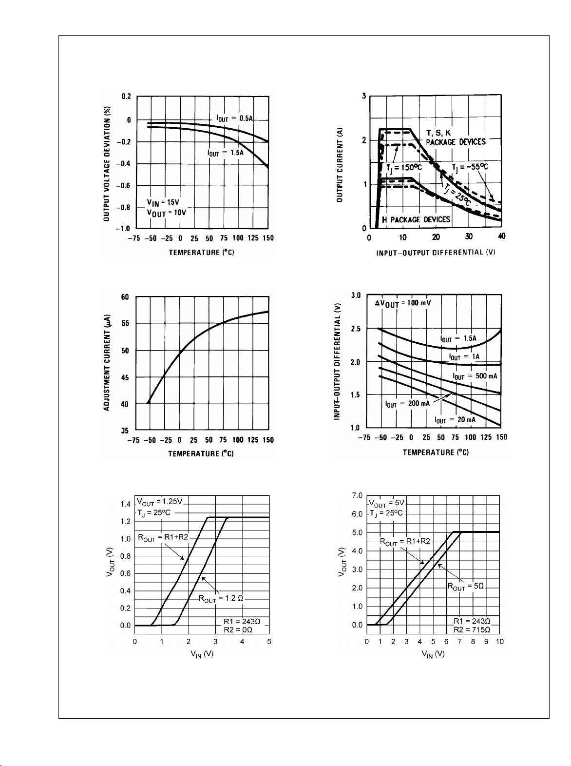
Typical Performance Characteristics Output Capacitor = 0 μF unless otherwise noted
LM117/LM317A/LM317
Adjustment Current
Load Regulation
906337
Current Limit
906338
Dropout Voltage
906339
V
vs VIN, V
OUT
www.national.com 6
OUT
= V
REF
906367
V
OUT
vs VIN, V
OUT
906340
= 5V
906368
LM117/LM317A/LM317
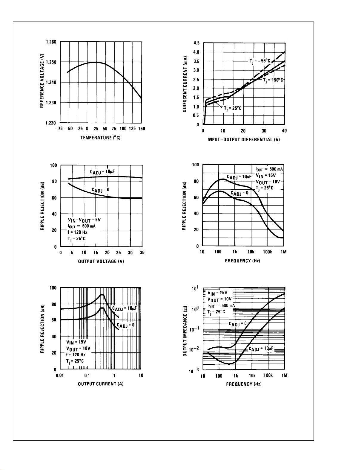
Temperature Stability
Ripple Rejection
906341
Minimum Operating Current
906342
Ripple Rejection
Ripple Rejection
906343
906345
906344
Output Impedance
906346
7 www.national.com
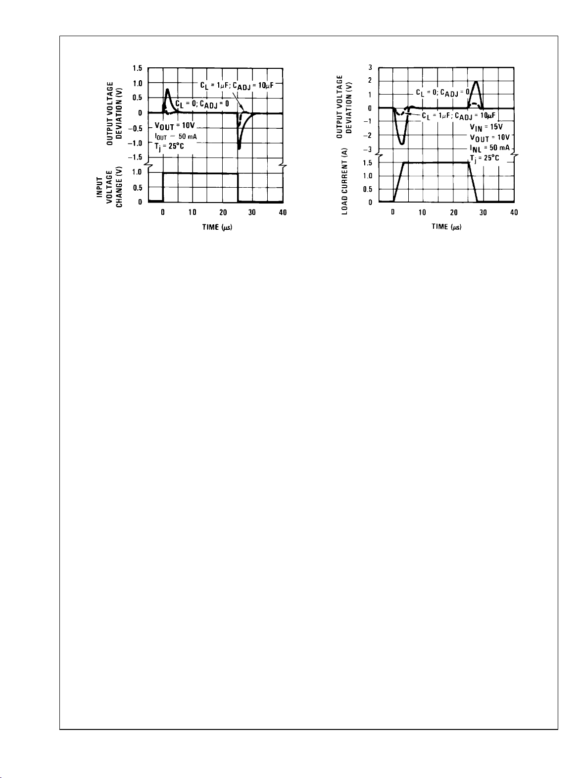
Line Transient Response
LM117/LM317A/LM317
Load Transient Response
906347
906348
www.national.com 8
LM117/LM317A/LM317
Application Hints
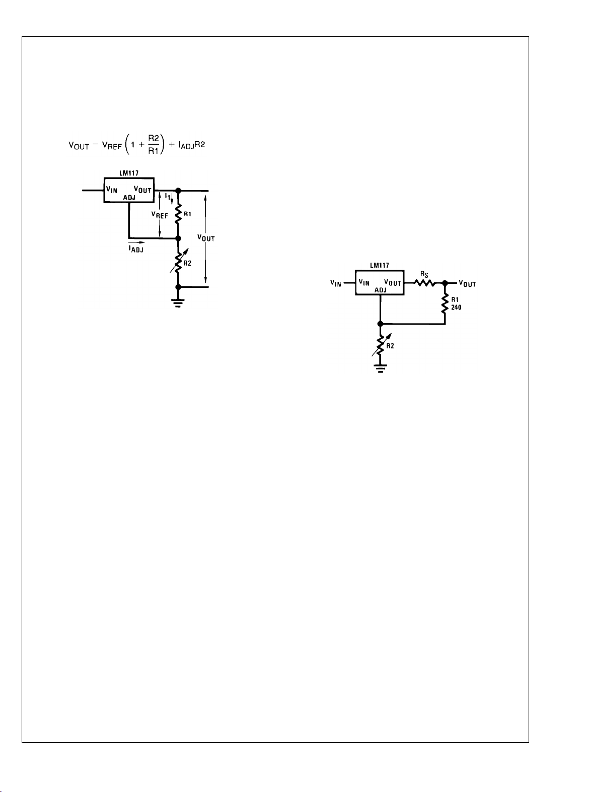
In operation, the LM117 develops a nominal 1.25V reference
voltage, V
The reference voltage is impressed across program resistor
R1 and, since the voltage is constant, a constant current I
then flows through the output set resistor R2, giving an output
voltage of
, between the output and adjustment terminal.
REF
906305
FIGURE 1.
(1)
aluminum electrolytic) on the output swamps this effect and
insures stability. Any increase of the load capacitance larger
than 10 μF will merely improve the loop stability and output
impedance.
1
LOAD REGULATION
The LM117 is capable of providing extremely good load regulation but a few precautions are needed to obtain maximum
performance. The current set resistor connected between the
adjustment terminal and the output terminal (usually 240Ω)
should be tied directly to the output (case) of the regulator
rather than near the load. This eliminates line drops from appearing effectively in series with the reference and degrading
regulation. For example, a 15V regulator with 0.05Ω resistance between the regulator and load will have a load regulation due to line resistance of 0.05Ω × IL. If the set resistor is
connected near the load the effective line resistance will be
0.05Ω (1 + R2/R1) or in this case, 11.5 times worse.
Figure 2 shows the effect of resistance between the regulator
and 240Ω set resistor.
Since the 100μA current from the adjustment terminal represents an error term, the LM117 was designed to minimize
I
and make it very constant with line and load changes. To
ADJ
do this, all quiescent operating current is returned to the output establishing a minimum load current requirement. If there
is insufficient load on the output, the output will rise.
EXTERNAL CAPACITORS
An input bypass capacitor is recommended. A 0.1μF disc or
1μF solid tantalum on the input is suitable input bypassing for
almost all applications. The device is more sensitive to the
absence of input bypassing when adjustment or output capacitors are used but the above values will eliminate the
possibility of problems.
The adjustment terminal can be bypassed to ground on the
LM117 to improve ripple rejection. This bypass capacitor prevents ripple from being amplified as the output voltage is
increased. With a 10 μF bypass capacitor 80dB ripple rejection is obtainable at any output level. Increases over 10 μF do
not appreciably improve the ripple rejection at frequencies
above 120Hz. If the bypass capacitor is used, it is sometimes
necessary to include protection diodes to prevent the capacitor from discharging through internal low current paths and
damaging the device.
In general, the best type of capacitors to use is solid tantalum.
Solid tantalum capacitors have low impedance even at high
frequencies. Depending upon capacitor construction, it takes
about 25 μF in aluminum electrolytic to equal 1μF solid tantalum at high frequencies. Ceramic capacitors are also good
at high frequencies; but some types have a large decrease in
capacitance at frequencies around 0.5 MHz. For this reason,
0.01 μF disc may seem to work better than a 0.1 μF disc as
a bypass.
Although the LM117 is stable with no output capacitors, like
any feedback circuit, certain values of external capacitance
can cause excessive ringing. This occurs with values between 500 pF and 5000 pF. A 1 μF solid tantalum (or 25 μF
906306
FIGURE 2. Regulator with Line Resistance in Output Lead
With the TO-3 package, it is easy to minimize the resistance
from the case to the set resistor, by using two separate leads
to the case. However, with the TO-39 package, care should
be taken to minimize the wire length of the output lead. The
ground of R2 can be returned near the ground of the load to
provide remote ground sensing and improve load regulation.
PROTECTION DIODES
When external capacitors are used with any IC regulator it is
sometimes necessary to add protection diodes to prevent the
capacitors from discharging through low current points into
the regulator. Most 10 μF capacitors have low enough internal
series resistance to deliver 20A spikes when shorted. Although the surge is short, there is enough energy to damage
parts of the IC.
When an output capacitor is connected to a regulator and the
input is shorted, the output capacitor will discharge into the
output of the regulator. The discharge current depends on the
value of the capacitor, the output voltage of the regulator, and
the rate of decrease of VIN. In the LM117, this discharge path
is through a large junction that is able to sustain 15A surge
with no problem. This is not true of other types of positive
regulators. For output capacitors of 25 μF or less, there is no
need to use diodes.
The bypass capacitor on the adjustment terminal can discharge through a low current junction. Discharge occurs when
either the input, or the output, is shorted. Internal to the LM117
is a 50Ω resistor which limits the peak discharge current. No
protection is needed for output voltages of 25V or less and 10
μF capacitance. Figure 3 shows an LM117 with protection
9 www.national.com
 Loading...