

Philips LLE18300X Datasheet
DISCRETE SEMICONDUCTORS
DATA SH EET
M3D159
LLE18300X
NPN microwave power transistor
Product specification
Supersedes data of September 1994
1999 Apr 22
Philips Semiconductors Product specification
NPN microwave power transistor LLE18300X
FEATURES
Diffused emitter ballasting resistors
providing excellent current sharing
and withstanding a high VSWR
• Interdigitated structure provides
high emitter efficiency
• Gold metallization realizes very
good stability of the characteristics
and excellent lifetime
• Multicell geometry gives good
balance of dissipated power and
low thermal resistance
• Internal input and output
prematching ensures good stability
and allows an easier design of
wideband circuits.
APPLICATION
Intended for use in common emitter,
class AB amplifiers in CW conditions
for professional applications between
1.7 GHz and 2 GHz.
DESCRIPTION
NPN silicon planar epitaxial
microwave power transistor in an
SOT437A glued cap metal ceramic
flange package, with emitter
connected to flange.
QUICK REFERENCE DATA
Microwave performance up to T
=25°C in a common emitter class AB
mb
amplifier.
MODE OF
OPERATIONf(GHz)
V
(V)
CE
I
CQ
(A)
P
L1
(W)
G
po
(dB)
η
(%)
C
Zi; Z
(Ω)
Class AB (CW) 1.85 24 0.1 ≥27 ≥7.8 typ. 40 see Figs
8 and 9
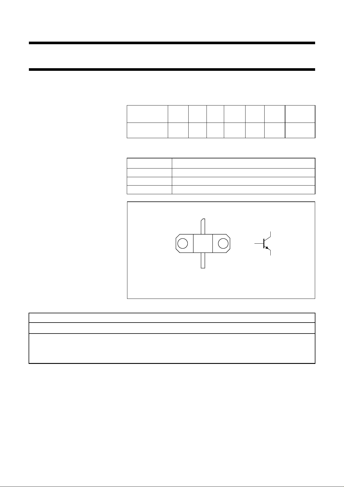
PINNING - SOT437A
PIN DESCRIPTION
1 collector
2 base
3 emitter connected to flange
handbook, 4 columns
Top view
1
c
b
3
2
e
MAM112
Fig.1 Simplified outline and symbol.
L
WARNING
Product and environmental safety - toxic materials
This product contains beryllium oxide. The product is entirely safe provided that the BeO disc is not damaged.
All persons who handle, use or dispose of this product should be aware of its nature and of the necessary safety
precautions. After use, dispose of as chemical or special waste according to the regulations applying at the location of
the user. It must never be thrown out with the general or domestic waste.
1999 Apr 22 2
Philips Semiconductors Product specification
NPN microwave power transistor LLE18300X
LIMITING VALUES
In accordance with the Absolute Maximum Rating System (IEC 134).
SYMBOL PARAMETER CONDITIONS MIN. MAX. UNIT
V
CBO
V
CER
V
CEO
V
EBO
I
C
P
i
P
tot
T
stg
T
j
T
sld
Note
1. Up to 0.2 mm from ceramic.
collector-base voltage open emitter − 45 V
collector-emitter voltage RBE= 220 Ω−30 V
collector-emitter voltage open base − 15 V
emitter-base voltage open collector − 3V
collector current (DC) − 6A
input power f = 1.85 GHz; VCE= 24 V; class AB − 8W
total power dissipation Tmb=75°C − 50 W
storage temperature −65 +150 °C
junction temperature − 200 °C
soldering temperature t ≤ 10 s; 1 − 235 °C
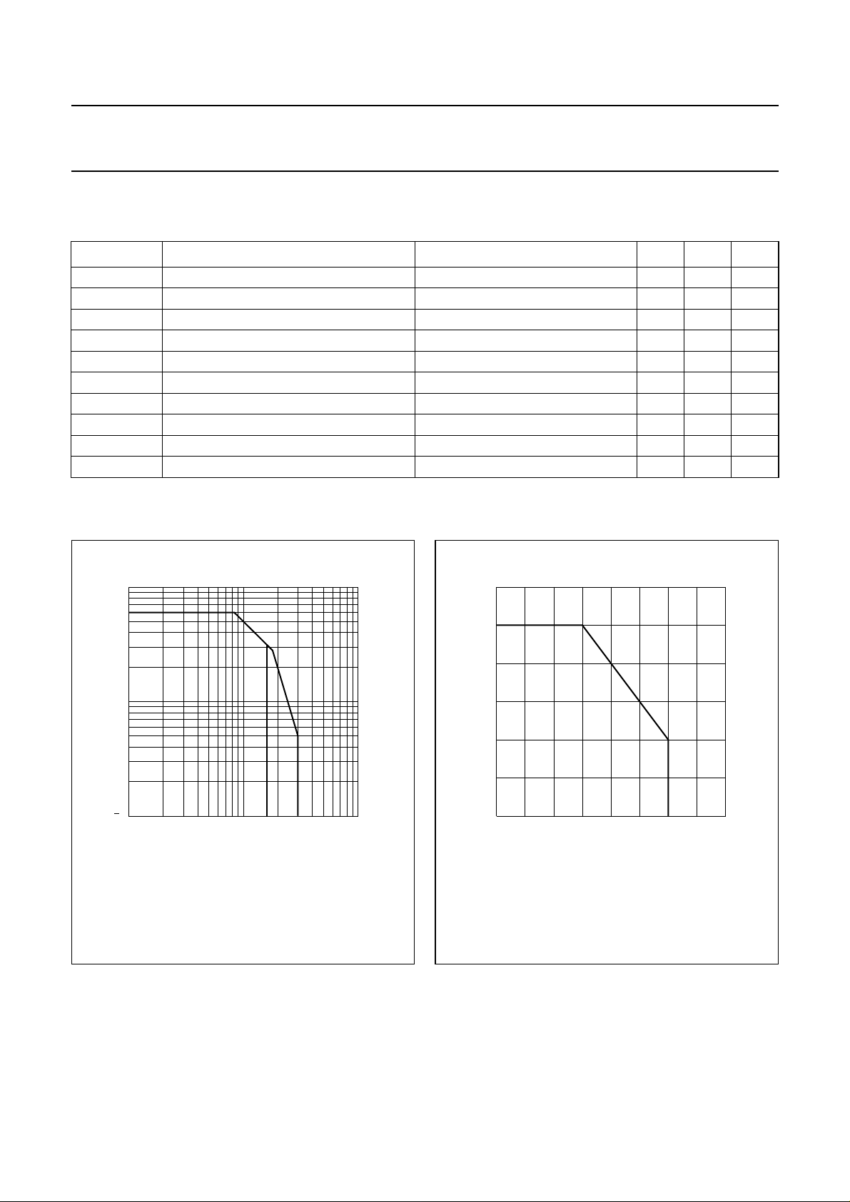
10
I
C
(A)
101
ΙΙΙ
V (V)
CE
1
1
10
Tmb≤ 75 °C.
(I) Region of permissible DC operation.
(II) Permissible extension provided RBE≤ 220 Ω.
Fig.2 DC SOAR.
MBD734
150
T ( C)
mb
MEA577
o
60
P
tot
(W)
40
20
2
10
0
0 50 100 200
Fig.3 Power derating curve.
1999 Apr 22 3
Philips Semiconductors Product specification
NPN microwave power transistor LLE18300X
THERMAL CHARACTERISTICS
SYMBOL PARAMETER CONDITIONS MAX. UNIT
R
th j-mb
R
th mb-h
CHARACTERISTICS
=25°C unless otherwise specified.
T
mb
SYMBOL PARAMETER CONDITIONS MIN. MAX. UNIT
I
CBO
V
(BR)CER
V
(BR)CBO
V
(BR)EBO
h
FE
thermal resistance from junction to mounting base Tj= 100 °C 2 K/W
thermal resistance from mounting base to heatsink 0.2 K/W
collector cut-off current IE= 0; VCB=20V − 3mA
collector-emitter breakdown voltage IC= 15 mA; RBE= 220 Ω 30 − V
collector-base breakdown voltage IC=15mA 45 − V
emitter-base breakdown voltage IE=15mA 3 − V
DC current gain IC= 1 A; VCE= 3 V 15 100
APPLICATION INFORMATION
Microwave performance up to T
MODE OF
OPERATION
f
(GHz)
=25°C in a common emitter class AB amplifier.
mb
V
(V)
CE
I
CQ
(A)
Class AB (CW) 1.85 24 0.1 ≥27
P
(W)
typ. 30
L1
G
(dB)
≥7.8
typ. 8.6
po
η
(%)
C
Zi; Z
(Ω)
L
typ. 40 see Figs 8
and 9
1999 Apr 22 4
 Loading...