

Page 1

Colour Television
LCD1.20E
AA
Contents Page
1 Technical Specifications, Connections,
and Chassis Overview 2
2 Safety Instructions, Warnings, and Notes 3
3 Directions for Use 6
4 Mechanical Instructions 8
5 Service Modes, Error messages,
and Repair Tips 9
6 Block Diagrams
Wiring Diagram 11
Block Diagram 11
7 Electrical Diagrams and PWB lay-outs Diagram PWB
Main Board 12-16 17-18
Control, Tuner, Speaker, and MX Panel 19
8 Electrical Alignments 21
9 Circuit Descriptions 23
Abbreviation List (N.A.)
IC Data Sheets (N.A)
10 Spare Parts List 24
11 Revision List 26
©
Copyright 2003 Philips Consumer Electronics B.V. Eindhoven, The Netherlands.
All rights reserved. No part of this publication may be reproduced, stored in a
retrieval system or transmitted, in any form or by any means, electronic,
mechanical, photocopying, or otherwise without the prior permission of Philips.
Published by LM 0369 Service PaCE Printed in the Netherlands Subject to modification EN 3122 785 12521
Page 2

EN 2 LCD1.20E1.
Technical Specifications, Connections, and Chassis Overview
1. Technical Specifications, Connections, and Chassis Overview
1.1 Technical Specifications
1.1.1 Reception
Tuning system : PLL
Colour systems : PAL B/G,
: PAL D/K,
: PAL I
: SECAM B/G,
: SECAM D/K,
: SECAM L,
: SECAM L1,
: NTSC Play Back
Sound systems : 2CS B/G,
Frequency bands : VHF,
Channel selections : 100 channels
Aerial input : 75 ohm
:
: 2CS D/K,
: AV Stereo,
: NICAM B/G
: (5.5-5.85),
: NICAM D/K
: UHF,
: S-Channel,
: Hyperband
1.1.2 LCD Characteristics
Type : LCD XGA TFT
Size : 20 inch (51 cm)
Pixel format : 640x480 pixels
1.1.3 Optical Characteristics
Contrast ratio : 400:1 (typ.)
Brightness : 450 cd/m2 typ.
Viewing Angle : 140x120 deg. (HxV)
1.1.4 Audio
Speakers : Full range
1.1.5 Miscellaneous
Power consumption
Normal operation : 70 W
Standby : 3 W
Power Supply
Power Adaptor
Input : AC 95 to 264 V, 50/60
Output : DC 12 V, 3 A
: 2 x 2 W_rms
Hz
Environment
Ambient temperature : +5 to +40 deg. C
Relative humidity : 10% to 80% R.H.
Weight : 9 kg
Dimension (WxHxD) : 642x423x83 m
Page 3
Safety Instructions, Warnings, and Notes
2. Safety Instructions, Warnings, and Notes
EN 3LCD1.20E 2.
2.1 Safety Instructions
• Always connect the TV set via an Insulation transformer.
Use a transformer of adequate power to protect the
technician from injury by electrical shocks. It will also
protect the TV set and it's components from being
damaged by accidental shorts of the circuitry, which may
be occurred during the service operation.
• Replace safety components, indicated by the symbol i in
the Schematic diagram and Replacement parts list, only by
the identical components to the original ones. Any other
component substitution (other than original type) may
increase risk of fire or electrical shock hazard.
• If any fuse (or Fusible resistor) in this TV set is blown,
replace it as specified.
• While replacing a high wattage resistor (Oxide Metal Film
Resistor, over 1 W), keep the resistor 10 mm away from
PCB.
• Keep wires away from high voltage or high temperature
parts.
2.1.1 AC Leakage Current Check
Before returning the TV set to the customer, always perform an
AC leakage current check on the exposed metallic parts of
the cabinet, such as antennas, terminals, etc., to be sure the
set is safe to operate without damage by electrical shock.
Leakage Current Cold Check (Antenna Cold Check)
1. Unplug the AC cord, and connect an electrical jumper
between the two plug prongs of the AC cord.
2. Turn “on” the AC power switch (keep the AC cord
unplugged!).
3. Measure the resistance value between the plug prongs of
the AC cord and the metal shielding of the tuner or the
aerial connection of the TV set. The measured resistance
should be between 1 Mohm and 5.2 Mohm. When the
metal shielding has no return path to the chassis, the
measured resistance must be infinite.
4. Switch the TV set “off’” and remove the electrical jumper
between the two plug prongs of the AC cord.
5. Check the cabinet for defects, to prevent the possibility of
the customer touching any internal parts.
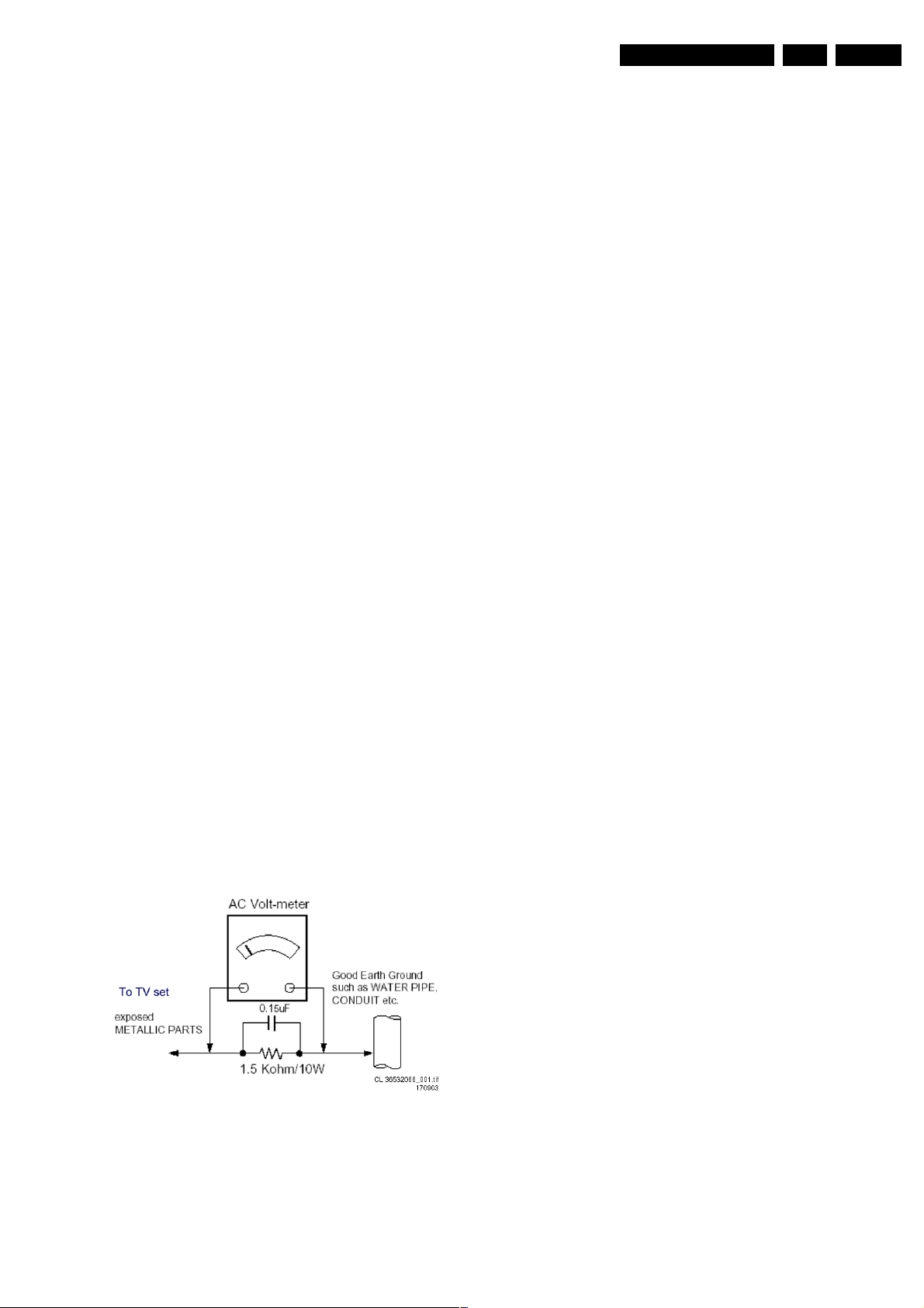
Leakage Current Hot Check
1. Plug the AC cord directly into the AC outlet.
2. Connect 1.5 kohm/10 W resistor in parallel with a 0.15 uF
capacitor between a good known earth ground (Water
Pipe, Conduit, etc.) and the exposed metallic parts.
3. Measure the AC voltage across the resistor, using the AC
voltmeter with 1000 ohm/V or higher sensitivity.
4. Plug again the AC cord into the AC outlet and repeat AC
voltage measurements for each exposed metallic part. Any
voltage measured must not exceed 0.75 V_rms, which
corresponds to 0.5 mA.
5. If any measurement is out of the specified limits, there is a
possibility of a shock hazard, and the set must be checked
and repaired before returning to the customer.
2.2 Warnings:
Before servicing TV sets, covered by this service manual and
its supplements and addenda, read and follow the Safety
Instructions of this manual.
Note: If unforeseen circumstances create conflict between the
following Servicing Precautions and any of the Safety
Instructions of this manual, always follow the Safety
Instructions. Remember: Safety First.
2.2.1 General Servicing Precautions
1. Always unplug the TV set AC power cord from the AC
power source before:
1. Removing or reinstalling any component, circuit board
module, or any other receiver assembly;
2. Disconnecting or reconnecting any TV set electrical
plug or other electrical connection;
3. Connecting a test substitute in parallel with an
electrolytic capacitor in the receiver.
Caution: A wrong part substitution or incorrect polarity
installation of electrolytic capacitors may result to an
explosion hazard.
2. Test high voltage only by measuring it with an appropriate
high voltage meter or other voltage measuring device
(DVM, FETVOM, etc), equipped with a suitable high
voltage probe. Do not test high voltage by "drawing an arc".
3. Do not spray chemicals on or near this TV set or any of its
assemblies.
4. Unless specified otherwise in this service manual, clean
electrical contacts only by applying the following mixture to
the contacts with a pipe cleaner, cotton-tipped stick or
comparable nonabrasive applicator; 10% (by volume)
Acetone and 90% (by volume) Isopropyl alcohol (90%-99%
strength).
Caution: This is a flammable mixture.
5. Unless specified otherwise in this service manual,
lubrication of contacts in not required.
6. Do not defeat any plug/socket B+ voltage interlocks, with
which the TV sets might be equipped.
7. Do not apply AC power to this TV set and/or any of its
electrical assemblies, unless all solid-state device heat
sinks are correctly installed.
8. Always connect the test TV set ground lead to the TV set
chassis ground before connecting the test TV set positive
lead.
9. Always remove the test TV set ground lead last.
10. Use with this TV set only the test fixtures, specified in this
service manual.
Figure 2-1 Leakage current hot check circuit
Note: Do not use a line Insulation transformer during this
check.
Caution: Do not connect the test fixture ground strap to any
heat sink in this TV set.
Page 4

EN 4 LCD1.20E2.
Safety Instructions, Warnings, and Notes
2.2.2 Electrostatically Sensitive (ES) Devices
Some semiconductor (solid state) devices can be damaged
easily by static electricity. Such components commonly are
called Electrostatically Sensitive (ES) Devices. Examples of
typical ES devices are integrated circuits and some field-effect
transistors and semiconductor "chip" components. The
following techniques should be used to help to reduce the
incidence of component damage, caused by static electricity.
1. Immediately before handling any semiconductor
component or semiconductor-equipped assembly, drain off
any electrostatic charge on your body by touching a known
earth ground. Alternatively, obtain and wear a
commercially available discharging wrist strap device,
which should be removed to prevent potential shock
reasons prior to applying power to the unit under test.
2. After removing an electrical assembly, equipped with ES
devices, place the assembly on a conductive surface, such
as aluminium foil, to prevent electrostatic charge build-up
or exposure of the assembly.
3. Use only a grounded-tip soldering iron to solder or unsolder
ES devices.
4. Use only an anti-static type solder removal device. Some
solder removal devices, not classified as "anti-static", can
generate electrical charges, sufficient to damage ES
devices.
5. Do not use freon-propelled chemicals. These can generate
electrical charges, sufficient to damage ES devices.
6. Do not remove a replacement ES device from its protective
package, until immediately before you are ready to install
it. (Most replacement ES devices are packed r with leads
electrically shorted together by conductive foam,
aluminium foil or comparable conductive material).
7. Immediately before removing the protective material from
the leads of a replacement ES device, touch the protective
material to the chassis or circuit assembly, into which the
device will be installed.
Caution: Be sure no power is applied to the chassis or
circuit, and observe all other safety precautions.
8. Minimize bodily motions, when handling unpackaged
replacement ES devices. (Otherwise harmless motion,
such as the brunching together of your clothes fabric or the
lifting of your foot from a carpeted floor, can generate static
electricity, sufficient to damage an ES device).
2.2.3 General Soldering Guidelines
1. Use a grounded-tip, low-wattage soldering iron and
appropriate tip size and shape, that will maintain tip
temperature within the range of 500 deg. F to 600 deg. F.
2. Use an appropriate gauge of RMA resin-core solder
composed of 60 parts tin/40 parts lead.
3. Keep the soldering iron tip clean and well tinned.
4. Thoroughly clean the surfaces to be soldered. Use a small
wire-bristle brush (0.5 inch or 1.25cm) with a metal handle.
Do not use freon-propelled spray-on cleaners.
5. Use the following unsoldering technique:
1. Allow the soldering iron tip to reach normal
temperature (500 deg. F to 600 deg. F).
2. Heat the component lead until the solder melts.
3. Quickly draw the melted solder with an anti-static,
suction-type solder removal device or with solder braid.
Caution: Work quickly to avoid overheating the circuit
board printed foil.
6. Use the following soldering technique:
1. Allow the soldering iron tip to reach the normal
temperature (500 deg. F to 600 deg. F).
2. First, hold the soldering iron tip and solder the strand
against the component lead until the solder melts.
3. Quickly move the soldering iron tip to the junction of the
component lead and the printed circuit foil, and hold
there only until the solder flows onto and around of the
both of the component lead and the printed circuit foil.
Caution: Work quickly to avoid overheating the circuit
board printed foil.
4. Closely inspect the solder area and remove any
excess or splashed solder with a small wire-bristle
brush.
2.3 Maintenance Instructions
2.3.1 IC Remove/Replacement
Some chassis circuit boards have slotted holes (oblong),
through which the IC leads are inserted and then bent flat
against the circuit foil. When holes are the slotted type, the
following technique should be used to remove and replace the
IC.
Removal
1. Desolder and straighten each IC lead in one operation, by
gently prying up the lead with the soldering iron tip, as the
solder melts.
2. Draw away the melted solder with an anti-static suction
type solder removal device (or with solder braid) before
removing the IC.
Replacement
1. Carefully insert the replacement IC in the circuit board.
2. Carefully bend each IC lead against the circuit foil pad and
solder it.
3. Clean the soldered areas with a small wire-bristle brush. It
is not necessary to reapply acrylic coating to the areas.
2.3.2 "Small-Signal" Discrete Transistor Removal/ Replacement
1. Remove the defective transistor by clipping its leads as
close as possible to the component body.
2. Bend into a "U" shape the end of each of three leads,
remaining on the circuit board.
3. Bend into a "U" shape the replacement transistor leads.
4. Connect the replacement transistor leads to the
corresponding leads, extending from the circuit board, and
crimp the "U" with long nose pliers to insure metal to metal
contact. Then solder each connection.
2.3.3 Power Output, Transistor Device Removal/ Replacement
1. Heat and remove all solder all around from the transistor
leads.
2. Remove the heat sink mounting screw (if so equipped).
3. Carefully remove the transistor from the heat sink of the
circuit board.
4. Insert a new transistor in the circuit board.
5. Solder each transistor lead, and clip off excess lead.
6. Replace the heat sink.
2.3.4 Diode Removal/ Replacement
1. Remove defective diode by clipping its leads as close as
possible to diode body.
2. Bend the two remaining leads perpendicular to the circuit
board.
3. Observing diode polarity, wrap each lead of the new diode
around the corresponding lead on the circuit board.
4. Securely crimp each connection and solder it.
5. Inspect (on the circuit board copper side) the solder joints
of the two "original" leads. If they are not shiny, reheat them
and, if necessary, apply additional solder.
2.3.5 Fuse and Conventional Resistor Removal/ Replacement
1. Clip each fuse or resistor lead at the top of the circuit board
hollow stake.
Page 5

Safety Instructions, Warnings, and Notes
EN 5LCD1.20E 2.
2. Securely crimp the leads of replacement component
around notch at stake top.
3. Solder the connections.
Caution: Maintain original spacing between the replaced
component and adjacent components and the circuit board to
prevent excessive component temperatures.
2.3.6 Circuit Board Foil Repair
Excessive heat applied to the copper foil of any printed circuit
board will weaken the adhesive that bonds the foil to the circuit
board, causing the foil to separate from or "lift-off" the board.
The following guidelines and procedures should be followed
whenever this condition is encountered.
At IC Connections
To repair a defective copper pattern at IC connections, use the
following procedure to install a jumper wire on the copper
pattern side of the circuit board. (Use this technique only on IC
connections).
1. Carefully remove the damaged copper pattern with a sharp
knife. (Remove only as much copper as absolutely
necessary).
2. Carefully scratch away the solder resist and acrylic coating
(if used) from the end of the remaining copper pattern.
3. Bend a small "U" in one end of a small gauge jumper wire
and carefully crimp it around the IC pin. Solder the IC
connection.
4. Route the jumper wire along the path of the out-away
copper pattern and let it overlap the previously scraped end
of the good copper pattern. Solder the overlapped area and
clip off any excess jumper wire.
2.4 Notes
2.4.1 Schematic Notes
• All resistor values are in ohms and the value multiplier is
often used to indicate the decimal point location (e.g. 2K2
indicates 2.2 kohm).
• Resistor values with no multiplier may be indicated with
either an "E" or an "R" (e.g. 220E or 220R indicates 220
ohm).
• All capacitor values are expressed in micro-farads (µ= x
10^-6), nano-farads (n= x 10^-9), or pico-farads (p= x 10^-
12).
• Capacitor values may also use the value multiplier as the
decimal point indication (e.g. 2p2 indicates 2.2 pF).
• An "asterisk" (*) indicates component usage varies. Refer
to the diversity tables for the correct values.
• The correct component values are listed in the Electrical
Replacement Parts List. Therefore, always check this list
when there is any doubt.
At Other Connections
Use the following technique to repair the defective copper
pattern at connections, other than IC Pins. This technique
involves the installation of a jumper wire on the component side
of the circuit board.
1. Remove the defective copper pattern with a sharp knife.
Remove at least 1/4 inch of copper, to ensure that a
hazardous condition will not exist if the jumper wire opens.
2. Trace along the copper pattern from both sides of the
pattern break and locate the nearest component that is
directly connected to the affected copper pattern.
3. Connect insulated 20-gauge jumper wire from the lead of
the nearest component on one side of the pattern break to
the lead of the nearest component on the other side.
4. Carefully crimp and solder the connections.
Caution: Be sure the insulated jumper wire is dressed so it
does not touch components or sharp edges.
Page 6
EN 6 LCD1.20E3.
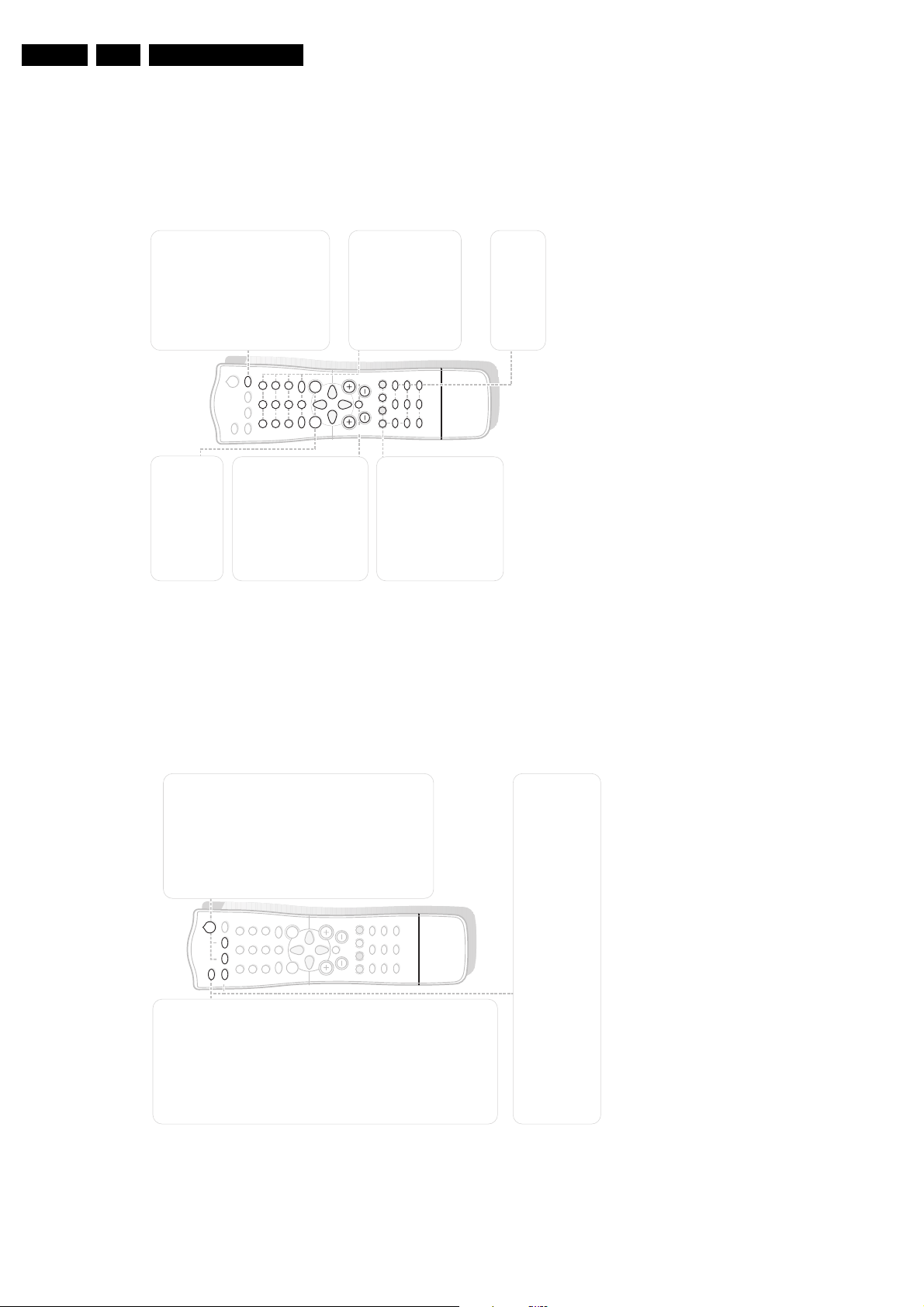
B
M
a
AUTO
AUTO
w
Y-Z
C
h
fg
c
b
e
k
Ò
‡
π
®
†
U
D
1
2
9
3
6
5
7
4
8
0
0
LIST
MENU
OK
P
¬
V
V Volum e
Press + or - to adjust the
vo lum e.
¬ Mute
Tem porarily interrupt the
sound or restore it.
P Programme selection
•to brow se through the TV
channels which are no t
skipped
•to sw itch the TV on fro m
standb y.
®Ò‡π† Video
reco rd er keys
U Time disp lay
The time,downloaded fro m the
TV channel (with teletext
broadcast) stored on
programme num ber 1 or the
low est not sk ipped programme
num ber,is displayed on the
screen.
0/9Digit keys
To select a TV channel.
0 Previous programme
To disp lay the previously
selectedTV channel.
LIST
Programme list
To disp lay the programme list.
b Teletext on/off
Teletext functions
hUfgcek
D
Sleep timer
With this key you can set a
time period after which the
TV sho uld sw itch itself to
standb y.
Press the key rep e atedly to
select the num ber of minutes.
The counter runs fro m B 0,
10,20,30...to 240 minutes.
The timer begins to count
dow n fro m the num ber of
minutes selected.
Note:To view the rem aining time,
pre ss the
D
key once.To can cel
the sleep time,repeatedly press
the
D
key until B 0 appears.
MENU
Press rep e a tedly to
display each menu.
O K Press this key to activate
yo ur cho ice,w hen in the menus.
3. Directions for Use
Directions for Use
picture
keys
AUTO
a
and sound se ttings.
To select predefined picture
AUTO
standb y or off to standb y.
Sw itche s the TV on fro m
B Standby
D
B
M
AUTO
a
AUTO
w
Y-Z
selected,corresponding with
different picture se tting is
Each time it is pre ssed,a
9
3
6
LIST
2
8
5
0
0
7
4
1
sound
AUTO
Contrast,Brigh tne ss,C o lour
and Sharpness.
M
spe c ific factory settings of
OK
MENU
different sound se tting is
Each time it is pre ssed,a
P
¬
V
refers to the personal
in the picture and sound menu.
and sound se lected an d stored
preference se ttings of picture
treb le an d bass.
selected,corresponding with
spe c ific factory settings of
Perso nal
π
k
b
‡
e
fg
C
h
Ò
c
U
†
®
DESCRIPTION OF CONTROLS
AV1,AV2,S-VIDEO
,
TV
Source
peripherals:p re ss rep e atedly to
select
Select you r com puter or other
w
monitor mode.
PC
or
X Bilingual cho ice an d
to
Nicam
Stereo
to
sound in case of
Mono
Nicam Stereo
stereo tran sm ission,or fro m
• to sw itch fro m
Press this key
sound mode selection
,in case of digital
Mono
tran sm ission
lY,
Dua
Z or
Nicam Dual
• to sw itch fro m
X in case
X in case of
Dual
Z or
Nicam Dual
Y to
Nicam Dual
Y se nd s the primary
of bilingual tran sm ission:
Dual
Dual
Nicam Dual tran sm ission
broadcast language to the
• to choose betw een
Z se nd s the seco n d ar y
loudspeakers;
Dual
loudspeakers;
broadcast language to the
X se nd s a se p ara te
Dual
lan guage to each loudspeaker.
Nica m stereo transm ission,select
sound sign als,w ith stereo or
Note:in case of weak stereo
fro m the aud io R input to the righ t loudspeaker
•R+R:the audio sign al fro m the au d io R input is se nt to the left and right loudspeakers.
•L+L:the audio sign al fro m the au d io L input is sent to the left an d righ t loudspeakers
•L+R:the audio signal fro m the au d io L input is sent to the left loudspeaker,the au dio signal
Press the X ke y rep e atedly to select:
Sound output se lection in AV mode
mono reception.
In AV mode,you can select the output sound for the left and right loudspeakers.
Page 7
Directions for Use
EN 7LCD1.20E 3.
Personal Notes:
ON/OFF
B
+
CH/PR
_
+
VOL
_
OK
TV/VIDEO MENU
monitor mode
PC
or
AV
,
TV
key to sw itch the TV on or off
ON/OFF
:P ress the power
in fro nt of the TV.
Sho uld your rem o te co n trol be lost or bro ken yo u can still operate yourTV with the keys
ON/OFF
:Keep the OK key p re ssed for abo u t 10 sec o n d s.
:P ress rep e atedly to select
Auto dem onstration
All the menus are being disp layed autom atically one after the other.
To stop Auto dem o nstratio n ,p re ss any key on the fro n t panel.
-
:P ress rep e atedly to display each menu
TV/VIDEO
MENU
OK: - P re ss this key to activate yo ur cho ice when in the menu
:- P ress - or + to brow se through the TV channels which are not sk ipped;
- Pre ss - or + to adjust the menu settings.
- Pre ss - or + to adjust the vo lum e;
:- P ress - or + to select a menu item ;
-V O L +
- CH /PR +
sw itch ed on.
-To sw itch the TV on fro m standb y.
- Pre ss - or + to select a menu item ;
TheB indicator ligh ts up brigh tly when the TV is in standby,dims when the TV is
B:Switches the TV on fro m stan db y or off to standb y.
Page 8

EN 8 LCD1.20E4.
Mechanical Instructions OLD!!!!
4. Mechanical Instructions OLD!!!!
Notes:
• To gain access to the boards of the TV set, after removing
the cover cup, unstick carefully supportive stickers.
• Place the stickers aside, adhesive side upwards.
• When you re-assemble the TV set, don’t forget to put the
stickers back.
• If the stickers are not adhesive anymore, you can order
them by ordering number 3104 301 24501
Page 9

Service Modes, Error Codes, and Fault Finding
5. Service Modes, Error Codes, and Fault Finding
5.1 General Features
Table 5-1 General Features
No. Symptom Cause Check Point
1 No screen Input error of inverter connector 1) Bend the pin legs of P801 connector -> recheck them
2) Check and repair the IC806, 807 SI4925, IC801 SI786, IC803 SI4808.
P502 and Pin 21 connector being
slipped out
Cracked components and soldering at tuner board
2 Dark screen 1) Defective LCD lamp
2) Defective inverter
3) Input error of inverter connector
3 Defective OSD display Defective the IC508 Check and replace the IC508
5.2 TV and External Input
Table 5-2 TV and External Input
1) Check and fix P503B connector
2) Check and fix the components at P502 LCD module and at main board.
3) Check Pin50.
1) Check and repair tuner board and main board
2) Solder Q101
1) Replace the LCD lamp 2) Replace the inverter
2) Check the connector input
EN 9LCD1.20E 5.
No. Symptom Cause Check Point
4 No sound
- Speaker
- Earphone
5 Video colour beat
noise
6 Video Jitter Defective P501B Pin20 connec-
Defective Reset IC of
IC902Defective MSP3410D of
IC901Defective B+ (8 V, 5 V) of
ICC903, 904.
Soldering IC201 and IC502,
IC501 or masking is short
tor
1) Check volume and speaker- Sound comes out only when being inputted
into Audio L/R
2) Check after replacing IC902
3) Replace IC901
4) Check and replace B+ of IC903, 904
Check and re-solder
Check the P501B Pin20 connector and repair
Page 10

EN 10 LCD1.20E5.
Personal Notes:
Service Modes, Error Codes, and Fault Finding
Page 11

Block Diagrams, Testpoint Overview, and Waveforms
11LCD1.20E 6.
6. Block Diagrams, Testpoint Overview, and Waveforms
Wiring Diagram
RE/RL - 20LA40 Wiring Diagram (20.1 ” )
To Panel
9965 000 20604
9965 000 16580
P803B
P501B
SC801
9965 000 16581
P503B
P501A
9965 000 20582
Tuner
9965 000 20605
P802B
P602
To Speaker
To Lamp
To Lamp
CL 36532069_002.eps
240903
LCD PANNEL
L
C
2
0
1
V
1
A
3
3.3V
VIDEO RAM
2M
R / G / B
8 /8 /8bit
15V
Dual Audio AMP
LA4282
Block Diagram
3.3V 5V(FOR RESET IC 3,3V)
SCALER(Format Converter)
MX88L-284FC-V
14.318MHz
8.0V
5.0V
Audio Processor
MSP-34XX
RF : 2, SCART : 4
MONO : 1
I2S : 2
------18.432MHz--L-SPK/WOOFER
H/P, I2S
SCART OUT : 2
R/G/B
24
RESET 4.2V
SCL/SDA
3.3V
AD Converter
AD9884AKS
9V
Multi-Component
Processor(BBVSP)
CXA 2101AQ
YCrCb : 2 / 4
RGB : 4 / 2
OUT RGB :1, TUV : 1
Y/U/V
(480P)
3.3V 3.3V
SCAN Converter
SDA-9410
27.0MHz
SCL/SDA
Analog
R/G/B/H/V
Y/U/V
(480P)
0.5-0.7
IC302
SCART(R/G/B/FB)
DVD-Y in(SCART-Vin)
SCL/SDA
Y/U/V
SCL/SDA
DVD-U/V in
4:2:2
(DRP Processor)
S-VHS(VIN1 : Y/C))
H/V
(2H)
R/G/B/FB
TEXT
SCL/SDA
IC301
H- FILTER
LGTV-1001
SWITCHING
CXA2040AQ
IC3
H-sync
CLK
Y/U/V
4:2:2
V-OUT
RF-IN
M/O(CVBS)
EEP
EEP
ROM
ROM
3.3V
SCL1/SDA1
IC1
MICOM / TXT
6.0MHz
480I/P
Detect
H-Sync.
SEP
5V 3.3V
IC201
Color Decoder/
A/D Converter
VPC-3230D
. COMB/FIL : 4H
INPUT . 4 CVBS . 1 S-VHS
. 2 RGB/YCrCb
. 1 F/B
. 1 CVBS OUTPUT
. Y/Cr/Cb OUTPUT
RF(VIN3 : CVBS)
M/O(CVBS)
TV/OUT(CVBS)
SCL/SDA
5V
3.3V
33V
BRI-ADJ TO MICOM
POWER-ON/OFF TO MICOM
20.25MHz
POWER
DC to DC Converter
(SI786,SI4808DY,T801)
DC to AC
INVEERTER
30V
5V
SCL
SDA
CVBS
15V
15V
R-SPK
L-SPK
DC OUT
(12V)
12V
REG.
AV2 in(CVBS)
R/G/B/FB L/ Rin TV/L/R out
Y/U/V in
. .
..
Y PB PR L R V L R V L R
SCART JACK
DVD/DTV
(480I/480P)
H/P S-VIDEO A/V IN
A/V OUT
DC IN
(15V)
SIF
IF AGC
TUNER
TUNER
ANT (RF)
CL 36532069_003.eps
240903
Page 12

Circuit Diagrams and PWB Layouts
7. Circuit Diagrams and PWB Layouts
Main Board (Overview)
Part 1
CL36532069_04a
12LCD1.20E 7.
Part 2
CL36532069_04b
Part 3
CL36532069_04c
Part 4
CL36532069_04d
CL 36532069_004.eps
240903
Page 13

Main Board (Part 1)
Circuit Diagrams and PWB Layouts
13LCD1.20E 7.
Part 1
CL 36532069_04a.eps
240903
Page 14

Main Board (Part 2)
of MF-004A
Circuit Diagrams and PWB Layouts
14LCD1.20E 7.
P/N : 3854VA0077A-S
DATE : 2000.10.02
Part 2
CL 36532066_04b.eps
170903
Page 15

Main Board (Part 3)
Circuit Diagrams and PWB Layouts
15LCD1.20E 7.
Part 3
CL 36532069_04c.eps
240903
Page 16

Main Board (Part 4)
Part 4
Circuit Diagrams and PWB Layouts
16LCD1.20E 7.
CL 36532069_04d.eps
240903
Page 17

Main Board (Top Side)
Circuit Diagrams and PWB Layouts
17LCD1.20E 7.
CL 36532069_005.eps
240903
Page 18

Circuit Diagrams and PWB Layouts
Main Board (Bottom Side)
18LCD1.20E 7.
CL 36532069_006.eps
240903
Page 19

Circuit Diagrams and PWB Layouts
19LCD1.20E 7.
Control, Tuner, and Speaker Panel
Control Panel (Top Side) Tuner Panel (Top Side)
TunerPanel (Bottom Side)
Control Panel (Bottom Side)
Top Panel (Top Side)
MX Panel
Top Side Bottom Side
CL 36532069_007.eps
240903
CL 36532069_008.eps
240903
Page 20

Personal Notes:
Circuit Diagrams and PWB Layouts
20LCD1.20E 7.
Page 21

8. Electrical Alignments
8.1 General Alignment Conditions
Note: This set uses an adapter, so connect the adapter and the
set correctly before adjustment.
Perform all electrical adjustments under the following
conditions:
• Temperature and humidity conditions: 25 ± 5 deg.C / 65 ±
10% RH
• Mains voltage and frequency: 220 to 240 V / 50 Hz.
• Allow the set to warm up for approximately 30 minutes.
• Test probe: Ri > 10 M ohm; Ci < 2.5 pF.
Notes:
The “Heat Run” must be performed with the full white signal or
the TV noise signal in the internal part of the set.
The time for the “Heat Run” can be changed, owing to
production plan.
8.2 Hardware Alignments
There are no hardware alignments foreseen for the LCD1.20E.
8.3 Software Alignments
8.3.1 Auto RGB Adjustment
Electrical Alignments
8.3.4 Default Option Adjustment
Note: This alignment is also implemented in ComPair.
1. Press the SVC key.
2. Use the SWAP/ADJUST key to find needed options or use
the OP1, OP2, OP3 keys.
3. Use the PR+/- key to select the option.
4. Use the VOL+/- key to change the value.
5. Press the OK key to store settings.
EN 21LCD1.20E 8.
Figure 8-1 Brightness adjustment
Required Equipment
A service remote control (9965 000 20079) or ComPair.
Preparation for Adjustment
Receive the Digital Pattern.
Adjustment
1. Select AUTO RGB ADJ by pressing SVC key.
2. Select “A RGB” item.
3. Press the VOL+/- key to appear “OK” on the screen.
8.3.2 RGB Level Adjustment
Required Equipment
• Pattern Generator (408NPS-READER), with possible 10
STEPs.
• A service remote control (9965 000 20079) or ComPair.
Adjustment
1. Select RGB Level by pressing SVC key.
2. Adjust than until 9th and 10th STEPs are undistinguished
by using VOL+/- key in R-LVL item.
3. Adjust G-LVL and B-LVL at the same way.
4. When adjustment is finished, store it by pressing the OK
key. Escape it by pressing the TV/AV key.
8.3.3 Brightness Adjustment
Use it in a case when brightness adjustment is needed.
Table 8-1 Default option settings
Option Code Function Remark Default
value
S-B 23
FP 21
NP 89
S1VOL 105
S2VOL 105
Table 8-2 Option 1
Option Code Function Remark Default
value
200PR
TEXT
I II SA
TOP
SCART
A2 ST
SYS
0 100 PROGRAM SAVE 0
1 200 PROGRAM SAVE
0 Without TXT 1
1With TXT
0No Save DUAL
SOUND Condition
1 Save DUAL SOUND
Condition
0 FLOF TEXT 1
1 TOP TEXT
0DVD JACK 1
1 SCART JACK
0 NICAM CHECK 1
1 NICAM and FM Stereo
0 B/G, I, D/K 0 (EU),
1 B/G, L/L
2 B/G, I, D/K, M
3 Reserved
0
1 (Fr)
Page 22

EN 22 LCD1.20E8.
Electrical Alignments
Table 8-3 Option 2
Option Code Function Remark Default
value
0 Without ACMS func-
ACMS
VOL
BBACK
LANG
(1) English, German, French, Italian, Spanish.
(2) English, Dutch, Swedish, Norwegian, Danish, Swiss,
Portuguese, Romanian, Polish, Hungarian, Czech, Russian.
(3) English, French, Arab, Urdu.
tion
1 With ACMS function
0Normal Volume Curve 0
1 Rushed Volume Curve
0 Without Blue Back 0
1 With Blue Back
0 English only English 6
1 English + EU4 (1)
2 English + other EU (2)
3 Farsi English,
4 Arab + Urdu (3)
5 English + China English,
6 Reserved
7 Reserved
Australia 1
Farsi
China
Option Code Function Remark Default
0 West Europe Teletext
Lan-
guage
1East Europe
2Turkey
3 Czech/Hungary
4 Cyrillic 1
5 Cyrillic 2
6 Cyrillic 3
T-LANG
7 Turkey/Greek 1
8 Turkey/Greek 2
9 Turkey/Greek 3
10 Arab/France
11 Arab/English
12 Arab/Hebrew 1
13 Arab/Hebrew 2
14 Farsi/English
15 Farsi/France
16 Farsi all
value
0
Table 8-4 Option 2
Option Code Function Remark Default
value
0 LOCAL KEY (20A20
KEY
TSS
PANEL
IICT
INVT
MD SA
MONO
CH+AU
MODEL)
1 LOCAL KEY (20LA30
MODEL)
0 Without TURBO
SEARCH function
1 With TURBO SEARCH
function
0 LCD Panel option 0
1 Reserved
0 Tuning with AFT Volt-
age
1 Tuning with ADC of IF
IC
0 INVERTER option 0
1 Reserved
0 Without LAST MODE
SAVE
1 With LAST MODE
SAVE
0 Without Forced MONO
sound system
1 With Forced MONO
sound system
0 Without D/K CHINA or
BB system
1 With D/K CHINA or BB
system
0
0
0
0
0
Page 23

Circuit Descriptions, List of Abbreviations, and IC Data Sheets
EN 23LCD1.20E 9.
9. Circuit Descriptions, List of Abbreviations, and IC Data Sheets
Not Applicable
Page 24

EN 24 LCD1.20E10.
10. Spare Parts List
Spare Parts List
LC1.20E
Various
00A1 9965 000 14322 DFU
00A2 9965 000 14330 RC25109/01
00A3 9965 000 14329 Adapter RF CAM-1550
00A4 9965 000 14331 Audio cable 2m
0112 9965 000 16522 LC201V1-A1
0120 9965 000 16523 Loudspeaker
0121 9965 000 16524 Tweeter C050D10K1452
0174 9965 000 14327 Mains cord for M2511A-
0174 9965 000 16412 Mains cord MP5004
0300 9965 000 16525 Cabinet
0310 9965 000 16526 Push buttons (7x)
0320 9965 000 16527 Coil
0330 9965 000 16528 Mains knob
0400 9965 000 16529 Rear cover
0401 9965 000 16591 Cover A/V
0410 9965 000 14325 Stand 20"
0520 9965 000 16531 Main board -/12S
0520 9965 000 16592 Main board -/19S
0530 9965 000 16532 MX panel
0540 9965 000 16533 Control panel
0570 9965 000 16534 Inverter 15V
0580 9965 000 16535 Tuner MF-002A EU
0580 9965 000 16593 Tuner MF-002A FR
FB801 9965 000 16454 Filter HH-1M3216-501
FB802 9965 000 16454 Filter HH-1M3216-501
P1001 9965 000 16580 Cable 12P 450mm
P1002 9965 000 16581 Cable 4P 450mm
P501 9965 000 20582 Cable P501A-P501B
P502 9965 000 20604 Cable P503B
P503 9965 000 20604 Cable P503B
P802 9965 000 20605 Cable P802B
PA1001 9965 000 16493 TSOP2238MQ1
PJ801 9965 000 16582 4P Power jack
S001 9965 000 16530 20" VESA PLATE
S002 9965 000 14332 VGA cable 7M
S030 9965 000 20079 Service RC
S031 3104 301 24501 Conductive sticker 50X35
SJ201 9965 000 16479 Socket scart
SW1001 9965 000 16502 SDKLA11100
SW1002 9965 000 16503 Tact switch
SW1003 9965 000 16503 Tact switch
SW1004 9965 000 16503 Tact switch
SW1005 9965 000 16503 Tact switch
SW1006 9965 000 16503 Tact switch
SW1007 9965 000 16503 Tact switch
SW1008 9965 000 16503 Tact switch
SY302 9965 000 16587 Filter TH355LSK-K5214
SY525 9965 000 16489 Filter 3216 4S600
SY526 9965 000 16489 Filter 3216 4S600
SY527 9965 000 16489 Filter 3216 4S600
SY532 9965 000 16489 Filter 3216 4S600
TU301 9965 000 16507 Tuner TAFC-M130D
TU301 9965 000 16521 Tuner TAFC-S120D
X1 9965 000 16508 Crystal 6 MHz HC49U
X301 9965 000 16588 Filter 27 MHz HC49U
X302 9965 000 16509 Crystal 20.250 MHz
X501 9965 000 16510 Crystal 14.318MHz
X601 9965 000 16510 Crystal 14.318MHz
X90 9965 000 16511 Crystal 500kHz
X901 9965 000 16512 Crystal 18.432 MHz
Z101 9965 000 16505 Filter MKT40.4MA110P-
Z101 9965 000 16520 Filter MKT41.4MA110P-
Z102 9965 000 16504 Filter MKT40.4MA110P-
ZD101 9965 000 16589 HZT33
C080L30K145X 5W/7W
001 EUR
1206
1206
SKHV17910B
SKHV17910B
SKHV17910B
SKHV17910B
SKHV17910B
SKHV17910B
SKHV17910B
HC49U
CSB500F9
HC49U
TF01
TF01
TF0
g
C1001 9965 000 16429 100µF 10V
C1002 9965 000 16430 0.01µF 80% 50V
C101 9965 000 16536 47µF 25V
C104 9965 000 16537 1000µF 10V
C107 9965 000 16434 10µF 50V
C111 9965 000 16432 100µF 16V
C112 9965 000 16435 4.7µF 50V
C112 9965 000 16441 22µF 16V
C205 9965 000 16432 100µF 16V
C206 9965 000 16438 220µF 16V
C211 9965 000 16441 22µF 16V
C217 9965 000 16441 22µF 16V
C240 9965 000 16439 220000pF 16V 0805
C241 9965 000 16439 220000pF 16V 0805
C243 9965 000 16435 4.7µF 50V
C248 9965 000 16439 220000pF 16V 0805
C249 9965 000 16439 220000pF 16V 0805
C250 9965 000 16439 220000pF 16V 0805
C251 9965 000 16439 220000pF 16V 0805
C252 9965 000 16435 4.7µF 50V
C253 9965 000 16439 220000pF 16V 0805
C255 9965 000 16439 220000pF 16V 0805
C257 9965 000 16439 220000pF 16V 0805
C262 9965 000 16538 0.47µF 50V SMD
C263 9965 000 16539 220µF 25V
C274 9965 000 16538 0.47µF 50V SMD
C275 9965 000 16435 4.7µF 50V
C276 9965 000 16540 330µF 16V
C278 9965 000 16432 100µF 16V
C280 9965 000 16435 4.7µF 50V
C281 9965 000 16435 4.7µF 50V
C284 9965 000 16541 33µF 16V
C289 9965 000 16542 1µF 50V
C343 9965 000 16433 47µF 16V
C349 9965 000 16431 10µF 16V
C402 9965 000 16433 47µF 16V
C408 9965 000 16543 0.47µF 50V
C417 9965 000 16433 47µF 16V
C418 9965 000 16431 10µF 16V
C418 9965 000 16544 10µF 16V
C419 9965 000 16542 1µF 50V
C422 9965 000 16543 0.47µF 50V
C423 9965 000 16431 10µF 16V
C423 9965 000 16544 10µF 16V
C431 9965 000 16545 47µF 50V
C435 9965 000 16546 100µF 16V
C438 9965 000 16547 1µF 50V
C439 9965 000 16548 470µF16V
C443 9965 000 16547 1µF 50V
C445 9965 000 16547 1µF 50V
C5 9965 000 16546 100µF 16V
C604 9965 000 16549 100µF 16V SMD
C606 9965 000 16549 100µF 16V SMD
C607 9965 000 16550 10µF 25V SMD
C627 9965 000 16549 100µF 16V SMD
C631 9965 000 16549 100µF 16V SMD
C640 9965 000 16551 220µF 6.3V SMD
C641 9965 000 16551 220µF 6.3V SMD
C7 9965 000 16432 100µF 16V
C7 9965 000 16546 100µF 16V
C801 9965 000 16545 47µF 50V
C802 9965 000 16432 100µF 16V
C802 9965 000 16546 100µF 16V
C803 9965 000 16548 470µF16V
C804 9965 000 16548 470µF16V
C805 9965 000 16548 470µF16V
C806 9965 000 16548 470µF16V
C807 9965 000 16552 220µF 25V
C812 9965 000 16552 220µF 25V
C814 9965 000 16435 4.7µF 50V
C816 9965 000 16448 100µF 25V
C819 9965 000 16431 10µF 16V
C820 9965 000 16539 220µF 25V
C826 9965 000 16553 330µF 25V
C827 9965 000 16548 470µF16V
C828 9965 000 16548 470µF16V
C871 9965 000 16444 470µF 16V
C872 9965 000 16553 330µF 25V
C880 9965 000 16548 470µF16V
C881 9965 000 16432 100µF 16V
C881 9965 000 16546 100µF 16V
C882 9965 000 16539 220µF 25V
C882 9965 000 16552 220µF 25V
C904 9965 000 16545 47µF 50V
C908 9965 000 16546 100µF 16V
C909 9965 000 16554 2.2µF 50V
C910 9965 000 16555 0.022µF 100V
C914 9965 000 16556 100µF 25V
C916 9965 000 16432 100µF 16V
C92 9965 000 16542 1µF 50V
C922 9965 000 16431 10µF 16V
C926 9965 000 16432 100µF 16V
C927 9965 000 16546 100µF 16V
C928 9965 000 16554 2.2µF 50V
C930 9965 000 16546 100µF 16V
C932 9965 000 16439 220000pF 16V 0805
C933 9965 000 16439 220000pF 16V 0805
C935 9965 000 16431 10µF 16V
C936 9965 000 16439 220000pF 16V 0805
C937 9965 000 16439 220000pF 16V 0805
C938 9965 000 16439 220000pF 16V 0805
C94 9965 000 16433 47µF 16V
C940 9965 000 16439 220000pF 16V 0805
C943 9965 000 16445 3.3µF 50V
C944 9965 000 16431 10µF 16V
C945 9965 000 16444 470µF 16V
C95 9965 000 16547 1µF 50V
C951 9965 000 16555 0.022µF 100V
C954 9965 000 16557 470µF 25V
C955 9965 000 16545 47µF 50V
C959 9965 000 16557 470µF 25V
C960 9965 000 16557 470µF 25V
f
R1001 9965 000 16498 4.7k 5% 1/6W
R1003 9965 000 16499 1.2k 5% 1/6W
R1004 9965 000 16500 330Ω 5% 1/6W
R1006 9965 000 16498 4.7k 5% 1/6W
R1007 9965 000 16498 4.7k 5% 1/6W
R1008 9965 000 16498 4.7k 5% 1/6W
R1009 9965 000 16498 4.7k 5% 1/6W
R1010 9965 000 16498 4.7k 5% 1/6W
R1011 9965 000 16498 4.7k 5% 1/6W
R250 9965 000 16501 120Ω 5% 1/2W
R253 9965 000 16501 120Ω 5% 1/2W
R321 9965 000 16583 22k 1% 1/6W
R322 9965 000 16584 56k 1% 1/6W
R932 9965 000 16585 5.6Ω 5% 2W
RA501 9965 000 16586 100Ω 5%
RA502 9965 000 16586 100Ω 5%
RA503 9965 000 16586 100Ω 5%
RA504 9965 000 16586 100Ω 5%
RA505 9965 000 16586 100Ω 5%
RA506 9965 000 16586 100Ω 5%
RA507 9965 000 16489 Filter 3216 4S600
b
L1 9965 000 16497 2N7000TA
L1001 9965 000 16482 22µH 2.3 X 3.4
L101 9965 000 16454 Filter HH-1M3216-501
L102 9965 000 16454 Filter HH-1M3216-501
L103 9965 000 16577 27µH 4.0 X 10.5
L2 9965 000 16497 2N7000TA
L201 9965 000 16485 12µH 2.3 X 3.4
L202 9965 000 16483 Filter HB-1M2012-800JT
L203 9965 000 16483 Filter HB-1M2012-800JT
L204 9965 000 16483 Filter HB-1M2012-800JT
L205 9965 000 16483 Filter HB-1M2012-800JT
L207 9965 000 16484 Filter HB-1S2012-080JT
L209 9965 000 16484 Filter HB-1S2012-080JT
L210 9965 000 16454 Filter HH-1M3216-501
L211 9965 000 16484 Filter HB-1S2012-080JT
L212 9965 000 16484 Filter HB-1S2012-080JT
L213 9965 000 16454 Filter HH-1M3216-501
L214 9965 000 16578 3.3µH 2.3 X 3.4
L215 9965 000 16484 Filter HB-1S2012-080JT
L216 9965 000 16484 Filter HB-1S2012-080JT
1206
1206
0805
0805
0805
0805
0805
0805
1206
0805
0805
1206
0805
0805
Page 25

Spare Parts List
EN 25LCD1.20E 10.
L217 9965 000 16454 Filter HH-1M3216-501
L218 9965 000 16454 Filter HH-1M3216-501
L219 9965 000 16454 Filter HH-1M3216-501
L220 9965 000 16454 Filter HH-1M3216-501
L221 9965 000 16454 Filter HH-1M3216-501
L305 9965 000 16454 Filter HH-1M3216-501
L306 9965 000 16454 Filter HH-1M3216-501
L307 9965 000 16454 Filter HH-1M3216-501
L308 9965 000 16454 Filter HH-1M3216-501
L309 9965 000 16454 Filter HH-1M3216-501
L310 9965 000 16454 Filter HH-1M3216-501
L311 9965 000 16454 Filter HH-1M3216-501
L312 9965 000 16484 Filter HB-1S2012-080JT
L401 9965 000 16454 Filter HH-1M3216-501
L402 9965 000 16454 Filter HH-1M3216-501
L403 9965 000 16454 Filter HH-1M3216-501
L511 9965 000 16484 Filter HB-1S2012-080JT
L512 9965 000 16484 Filter HB-1S2012-080JT
L519 9965 000 16483 Filter HB-1M2012-800JT
L601 9965 000 16454 Filter HH-1M3216-501
L602 9965 000 16454 Filter HH-1M3216-501
L603 9965 000 16454 Filter HH-1M3216-501
L801 9965 000 16488 26µH
L802 9965 000 16488 26µH
L803 9965 000 16454 Filter HH-1M3216-501
L804 9965 000 16487 9.5µH
L805 9965 000 16454 Filter HH-1M3216-501
L806 9965 000 16454 Filter HH-1M3216-501
L807 9965 000 16454 Filter HH-1M3216-501
L90 9965 000 16454 Filter HH-1M3216-501
L901 9965 000 16454 Filter HH-1M3216-501
L902 9965 000 16454 Filter HH-1M3216-501
L903 9965 000 16454 Filter HH-1M3216-501
L910 9965 000 16454 Filter HH-1M3216-501
LA801 9965 000 16489 Filter 3216 4S600
LA802 9965 000 16489 Filter 3216 4S600
LA803 9965 000 16489 Filter 3216 4S600
LA804 9965 000 16489 Filter 3216 4S600
LA805 9965 000 16489 Filter 3216 4S600
LA806 9965 000 16489 Filter 3216 4S600
LA811 9965 000 16489 Filter 3216 4S600
LA812 9965 000 16489 Filter 3216 4S600
LA813 9965 000 16489 Filter 3216 4S600
LA814 9965 000 16489 Filter 3216 4S600
LA815 9965 000 16489 Filter 3216 4S600
LD1001 9965 000 16490 LED assy
T801 9965 000 16506 Transformer 13-Z320UH
1206
1206
1206
1206
1206
1206
1206
1206
1206
1206
1206
1206
0805
1206
1206
1206
0805
0805
0805
1206
1206
1206
1206
1206
1206
1206
1206
1206
1206
1206
1206
DC-DC
d
D1 9965 000 16452 KDS181
D801 9965 000 16558 SM3411 (DL-11S2GN1)
D802 9965 000 16559 SR3411 (DL-11S2RN1)
D804 9965 000 16451 EU1ZV(1)
D804 9965 000 16452 KDS181
D805 9965 000 16452 KDS181
D806 9965 000 16452 KDS181
D807 9965 000 16452 KDS181
D901 9965 000 16452 KDS181
Y-Green
Red
D902 9965 000 16452 KDS181
ce
IC1 9965 000 16560 SDA555XF
IC10 9965 000 16459 LA7217M
IC2 9965 000 16456 AT24C16-10PC-2.7
IC201 9965 000 16561 VPC3230D QA
IC204 9965 000 16562 KIA7809API
IC3 9965 000 16563 CXA2040AQ
IC301 9965 000 16564 LGTV1001
IC302 9965 000 16565 SDA9410
IC303 9965 000 16566 Filter SMD H354LAI-
IC305 9965 000 16566 Filter SMD H354LAI-
IC4 9965 000 16458 KA75270Z
IC401 9965 000 16567 CXA2101AQ
IC402 9965 000 16568 PQ09RD21
IC501 9965 000 16569 THS8083
IC502 9965 000 16570 MX88L284-V
IC505 9965 000 16468 K4S161622D-TC80
IC506 9965 000 16474 SI4925DY
IC507 9965 000 16571 KIA7027AF
IC508 9965 000 16469 SC786107DWR2
IC509 9965 000 16572 KIA7033AF
IC801 9965 000 16475 SI786
IC802 9965 000 16573 SI4808DY
IC803 9965 000 16573 SI4808DY
IC806 9965 000 16474 SI4925DY
IC807 9965 000 16474 SI4925DY
IC808 9965 000 16474 SI4925DY
IC809 9965 000 16574 KIA7812API
IC850 9965 000 16568 PQ09RD21
IC851 9965 000 16457 PQ3RF23
IC852 9965 000 16575 KIA78L05BP
IC854 9965 000 16576 PQ12RF21
IC854 9965 000 16594 PQ12RD21
IC901 9965 000 16472 MSP3410D-QA-C5
IC902 9965 000 16572 KIA7033AF
IC903 9965 000 16461 KIA7808API
IC904 4822 209 16128 KIA7805PI
IC905 4822 209 31855 LA4282
Q1001 9965 000 16494 KTA-1266
Q101 9965 000 16495 2SC3875S
Q103 9965 000 16495 2SC3875S
Q104 9965 000 16495 2SC3875S
Q105 9965 000 16496 2SA1504S
Q106 9965 000 16495 2SC3875S
Q107 9965 000 16496 2SA1504S
Q201 9965 000 16495 2SC3875S
Q202 9965 000 16495 2SC3875S
Q203 9965 000 16495 2SC3875S
Q204 9965 000 16495 2SC3875S
Q205 9965 000 16495 2SC3875S
Q206 9965 000 16495 2SC3875S
Q207 9965 000 16495 2SC3875S
Q208 9965 000 16495 2SC3875S
Q209 9965 000 16495 2SC3875S
Q210 9965 000 16495 2SC3875S
Q211 9965 000 16496 2SA1504S
Q301 9965 000 16496 2SA1504S
Q302 9965 000 16496 2SA1504S
Q303 9965 000 16496 2SA1504S
Q304 9965 000 16496 2SA1504S
Q305 9965 000 16496 2SA1504S
Q306 9965 000 16496 2SA1504S
Q401 9965 000 16496 2SA1504S
Q402 9965 000 16496 2SA1504S
Q403 9965 000 16496 2SA1504S
Q404 9965 000 16495 2SC3875S
Q460 9965 000 16495 2SC3875S
Q50 9965 000 16495 2SC3875S
Q501 9965 000 16495 2SC3875S
Q801 9965 000 16495 2SC3875S
Q90 9965 000 16495 2SC3875S
Q901 9965 000 16496 2SA1504S
Q902 9965 000 16496 2SA1504S
Q903 9965 000 16496 2SA1504S
Q904 9965 000 16496 2SA1504S
Q905 9965 000 16496 2SA1504S
EJ201 9965 000 16480 Socket SHVS
MJ201 9965 000 16579 PJ6054P
K5206
K5206
Page 26

EN 26 LCD1.20E11.
11. Revision list
11.1 Manual 3122 785 12521
1. Wiring diagram is added.
2. Adjustment instruction is corrected.
3. Parts list is corrected
Revision list
 Loading...