

Page 1

Published by WS 0670 BG CD Customer Service Printed in the Netherlands Subject to modification EN 3122 785 15802
©
Copyright 2006 Philips Consumer Electronics B.V. Eindhoven, The Netherlands.
All rights reserved. No part of this publication may be reproduced, stored in a
retrieval system or transmitted, in any form or by any means, electronic,
mechanical, photocopying, or otherwise without the prior permission of Philips.
Colour Television Chassis
LC4.3HE
AA
Supplement to manual LC4.3E: 3122 785 15270
F_15800_000.eps
290906
Contents Page
1. Technical Specifications, Connections, and Chassis
Overview 2
2. Safety Instructions, Warnings, and Notes 3
3. Directions for Use 3
4. Mechanical Instructions 4
5. Service Modes, Error Codes, and Fault Finding 7
6.
Block Diagrams, Test Point Overviews, and
Waveforms
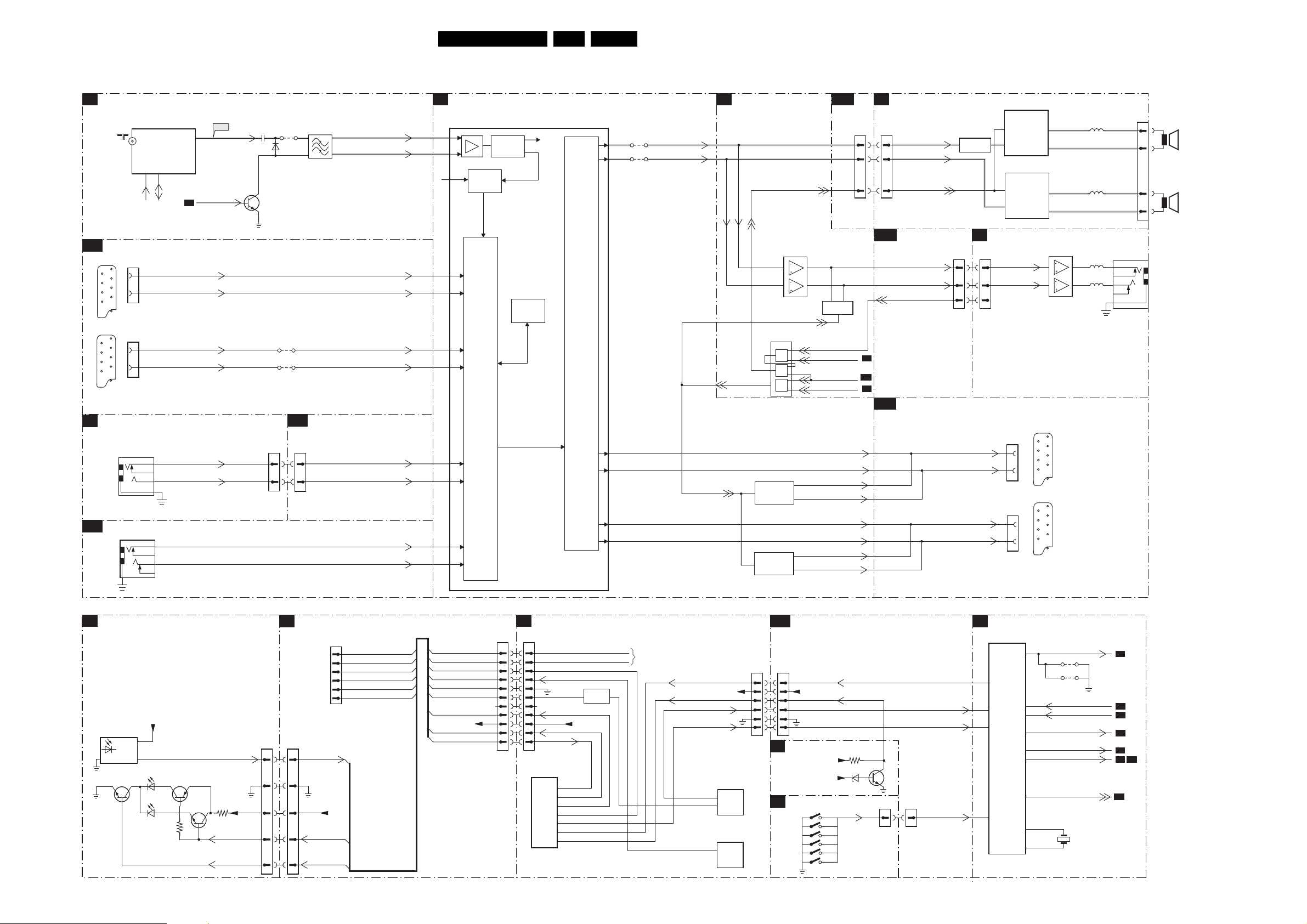
Wiring Diagram 9
Block Diagram Video 10
Block Diagram Audio 11
Testpoint Overview Small Signal Board 12
I2C IC Overview 13
Supply Voltage Overview 14
7.
Circuit Diagrams and PWB Layouts Drawing PWB
Side I/O Panel (D)15 16-16
LED and IR Panel (J) 17 18-18
i-Board Panel (HC) 19 20-20
LCD Clock Panel (O)21
8. Alignments 23
9. Circuit Descriptions, Abbreviation List, and IC Data
Sheets 26
Abbreviation List 26
IC Data Sheets 28
10. Spare Parts List 32
11. Revision List 38
Page 2
Technical Specifications, Connections, and Chassis Overview
EN 2 LC4.3HE AA1.
1. Technical Specifications, Connections, and Chassis Overview
Index of this chapter:
1.1 Technical Specifications
1.2 Connection Overview
1.3 Chassis Overview
Notes:
• Only information that is related to the iTV module, is
published in this manual. For the other information, see the
relevant chassis manual (order code on front page).
• Some models in this chassis range have a different
mechanical construction. The information given here is
therefore model specific.
• Figures below can deviate slightly from the actual situation,
due to the different set executions.
• Specifications are indicative (subject to change).
1.1 Technical Specifications
1.1.1 Vision
Display type : LCD WXGA Active
Matrix TFT
Screen size :
- 26HF5473/10 : 26” (66 cm), 16:9
- 32HF7473/10 : 32” (81 cm), 16:9
Resolution (HxV pixels) : 1366 x 768
Contrast ratio : 600:1
Light output (cd/m
2
) : 500
Response time (ms) : 16 (26”), 18 (32”)
Viewing angle (HxV degrees) : 176x176
Tuning system : PLL
Presets/channels : 125
Tuner bands : VHF
: UHF
: S-band
: Hyper-band
TV Colour systems : PAL B/G, D/K, I
: SECAM B/G, D/K, L/L’
Video playback : NTSC, PAL, SECAM
Supported computer formats : VGA (640x480)
: MAC (640x480)
: SVGA (800x600)
: XVGA (1024x768)
: WXGA (1280x768)
Supported video formats : 640x480i - 1fH
: 720x576i - 1fH
: 640x480p - 2fH
: 720x576p - 2fH
: 1920x1080i - 2fH
: 1280x720p - 3fH
1.1.2 Sound
Sound systems : FM, NICAM Stereo,
Virtual dolby surround
Maximum power (W
RMS
) : 2 x 5 (26”)
: 2 x 15 (32”)
1.1.3 Miscellaneous
Power supply:
- Mains voltage (V
AC
) : 100 - 250
- Mains frequency (Hz) : 50 / 60
Ambient conditions:
- Temperature range (°C) : +5 to +40
- Maximum humidity : 90% R.H.
Power consumption
- Normal operation (W) : 110 (26”), 120 (32”)
Dimensions (WxHxD cm) : 80.5x47.7x22.2 (26”)
: 92.4x55x22.2 (32”)
Weight (kg) : 18.8 (26”)
: 22 (32”)
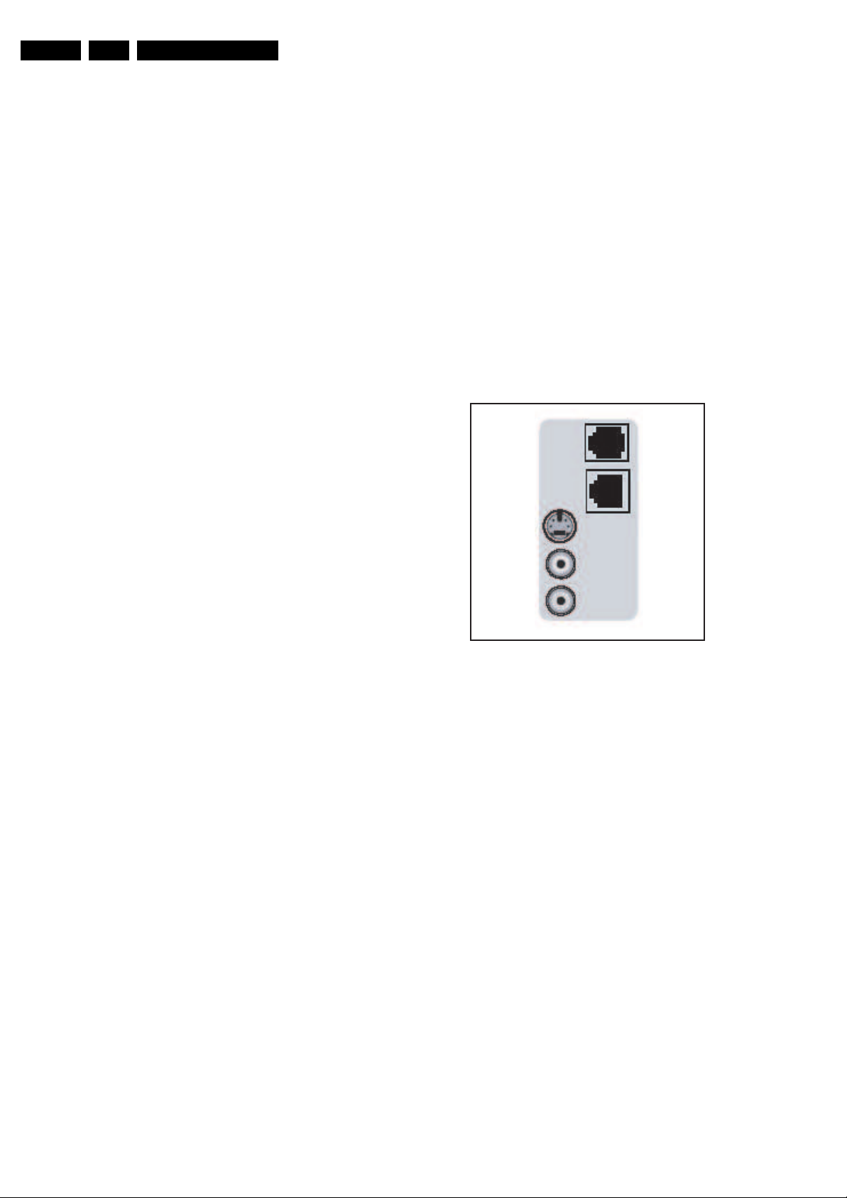
1.2 Connection Overview
Note: The following connector colour abbreviations are used
(acc. to DIN/IEC 757): Bk= Black, Bu= Blue, Gn= Green, Gy=
Grey, Rd= Red, Wh= White, and Ye= Yellow.
1.2.1 Side I/O connections
Figure 1-1 Side I/O connections
RJ12: DATA1 (HM-Link - In/Out)
1 -LED_in < 0.3 V, active low j
2 -IR_in < 0.3 V, active low j
3-MODE Vcc j
4 -TV Power Status 4.5 to 5 V - TV “On”, < 0.3V -
TV “Stdby”, High impedance -
TV “Off” k
5 -GND Gnd H
6 -IR_out Signal k
RJ45: DATA2 (Xpress Box- In/Out)
1 -+12V +12 V / 1 W k
2 -GND Gnd H
3 - HSYN Signal k
4 - VSYN Signal k
5 - TXD232 Signal
6 - RXD232 Signal
7 - SDA3_IR-OUT Signal k
8 - DCM-POR Signal k
9 - CVBS-terr Signal k
10 - GNDA Gnd H
SVHS (Hosiden): Video Y/C - In
1 - Ground Y Gnd H
2 - Ground C Gnd H
3 - Video Y 1 V
PP
/ 75 ohm j
4 - Video C 0.3 V
PP
/ 75 ohm j
F_15800_020.eps
241105
DATA 1
DATA 2
S-video
AV1 - in
Speaker
Page 3
Safety Instructions, Warnings, and Notes
EN 3LC4.3HE AA 2.
AV1 Mini Jack: Video 1fH CVBS - In, Audio - In
1 - Audio R 0.5 V
RMS
/ 10 kohm oj
2 - Ground CVBS Gnd oj
3 - Video CVBS 1 V
PP
/ 75 ohm oj
4 - Audio L 0.5 V
RMS
/ 10 kohm oj
Mini Jack: Speaker - Out
- Loudspeaker 8 ohm ok
1.2.2 Rear I/O connections
Rear connections are the same as for the LC4.3E.
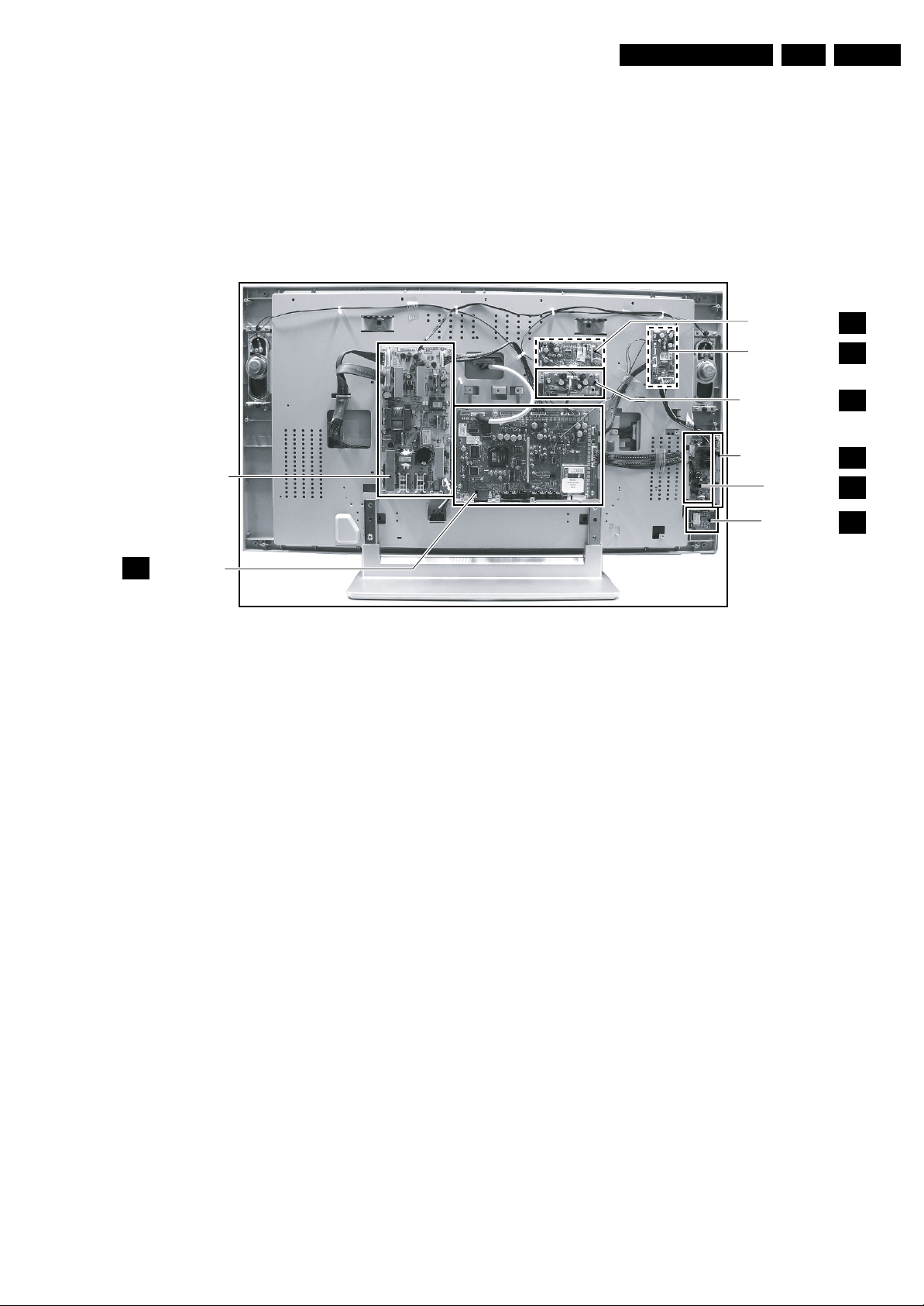
1.3 Chassis Overview
Figure 1-2 Chassis overview (both models)
2. Safety Instructions, Warnings, and Notes
See the relevant chassis manual (order code on front page).
3. Directions for Use
See the relevant chassis manual (order code on front page).
B
SMALL SIGNAL
BOARD
F_15800_003.eps
131205
D
SIDE I/O PANEL
E
J
LED & IR PANEL
C
AUDIO AMPL. PANEL
HC
iBOARD PANEL 26”
iBOARD PANEL 32”
(if present)
(if present)
HC
POWER SUPPLY
PANEL
KEYBOARD CONTOL
PANEL
Page 4
Mechanical Instructions
EN 4 LC4.3HE AA4.
4. Mechanical Instructions
Index of this chapter:
4.1 Cable Dressing
4.2 Service Position
4.3 Assy/Panel Removal
4.4 Set Re-assembly
Notes:
• Only information that is related to the iTV module, is
published in this manual. For other information, see the
relevant chassis manual (order code on front page).
• Figures below can deviate slightly from the actual situation,
due to the different set executions.
• Follow the disassembling instructions in described order.
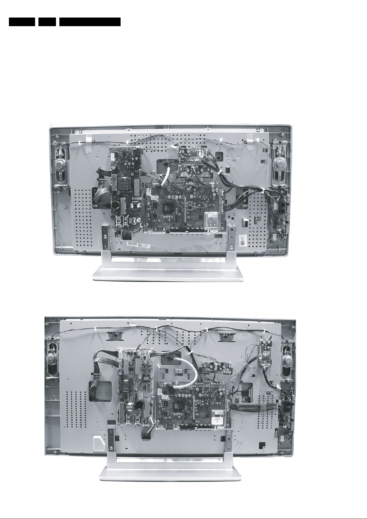
4.1 Cable Dressing
Figure 4-1 Cable dressing (26-inch model)
Figure 4-2 Cable dressing (32-inch model)
F_15800_002.eps
281105
F_15800_001.eps
281105
Page 5
Mechanical Instructions
EN 5LC4.3HE AA 4.
4.2 Service Position
First, put the TV set in its service position. Therefore, place it
upside down on a table top (use a protection sheet or foam
bars).
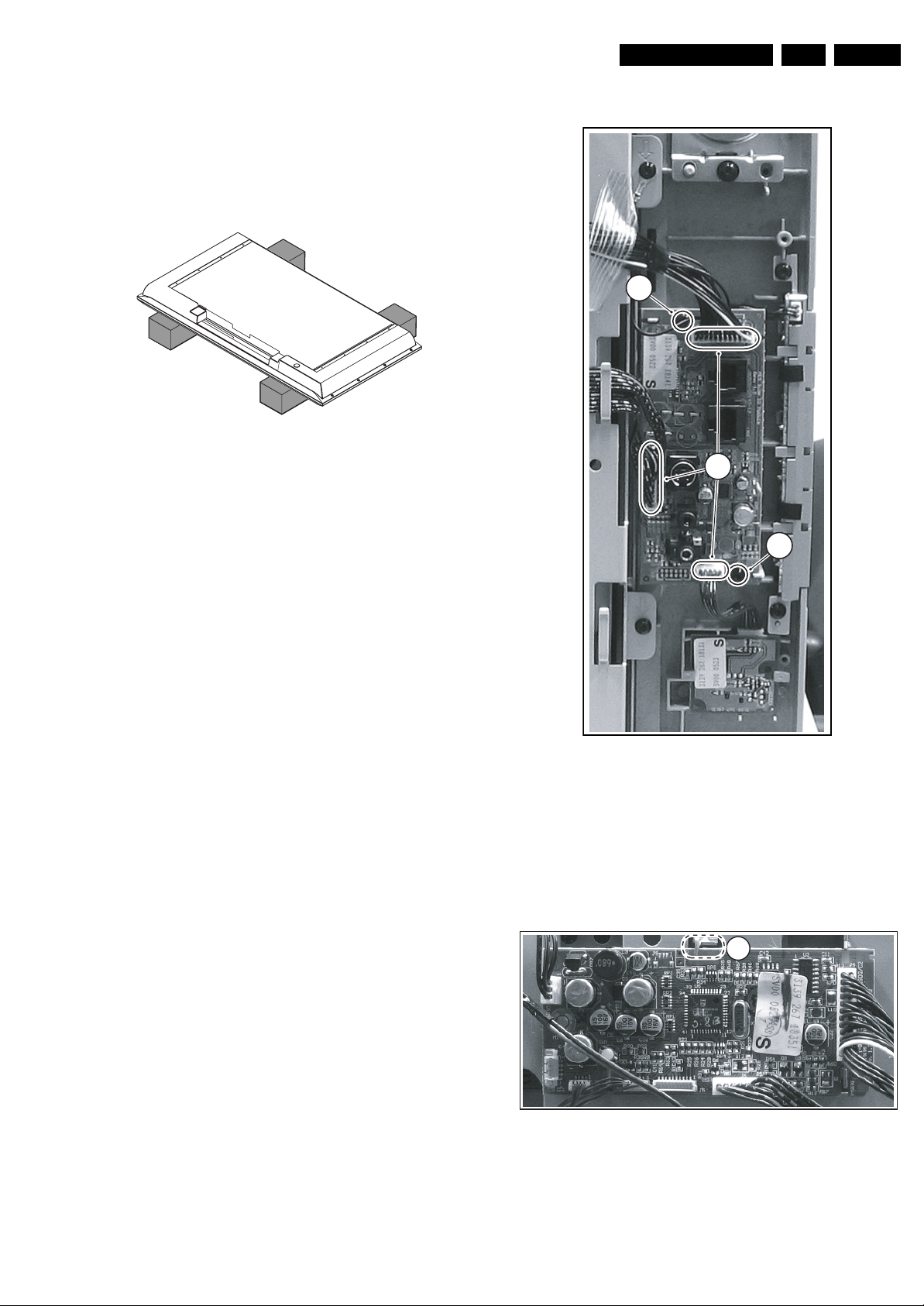
4.2.1 The Foam Bars
Figure 4-3 Foam bars
The foam bars (order code 3122 785 90580) can be used for
all types and sizes of Flat TVs. By laying the plasma or LCD TV
flat on the (ESD protective) foam bars, a stable situation is
created to perform measurements and alignments. By first
placing a mirror flat on the table under the TV you can easily
see if something is happening on the screen.
4.3 Assy/Panel Removal
4.3.1 Rear Cover
Warning: Disconnect the mains power cord before you remove
the rear cover.
1. Remove the screws that secure the rear cover.
2. Lift the rear cover from the cabinet cautiously. Make sure
that wires and other internal components are not damaged
during cover removal.
4.3.2 Side I/O & Keyboard Panel Removal
Figure 4-4 Side I/O & keyboard panel
1. Disconnect cables [1] from the panel (incl. the ground
cable).
2. Release the two fixation clamps [2] and lift the panel out of
the bracket.
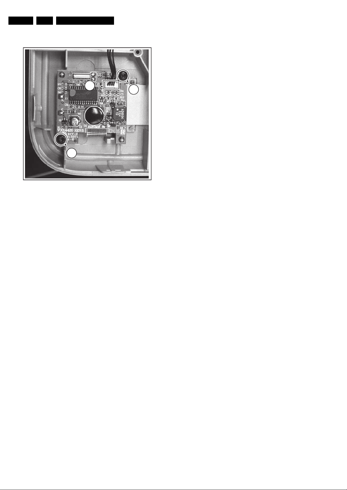
4.3.3 i-Board Removal
Figure 4-5 i-Board
1. Disconnect all cables [1] from the i-Board.
2. Untwist the fixation lip [2].
3. Take out the i-Board.
E_06532_018.eps
170504
F_15800_005.eps
071205
1
2
2
F_15800_004.eps
201205
1
Page 6
Mechanical Instructions
EN 6 LC4.3HE AA4.
4.3.4 Clock Panel Removal
Figure 4-6 Clock panel
1. Disconnect cable [1] from the Clock panel.
2. Remove the mounting crews [2] from the Clock panel.
3. Take out the Clock panel.
4.4 Set Re-assembly
To re-assemble the whole set, execute all processes in reverse
order.
Notes:
• While re-assembling, make sure that all cables are placed
and connected in their original positions. See Figure "Cable
dressing". Also make sure that the anti-static copper foils
are not damaged and that they make good electrical
contact with the metal frame. Be careful with the fragile
LVDS cable.
F_15140_013.eps
250105
2
2
1
Page 7
Service Modes, Error Codes, and Fault Finding
EN 7LC4.3HE AA 5.
5. Service Modes, Error Codes, and Fault Finding
Index of this chapter:
5.1 Hotel Mode, Service Modes
5.1 Hotel Mode, Service Modes
5.2 Error Codes
5.3 i-Board and LCD Clock
5.1 Hotel Mode, Service Modes
5.1.1 Hotel Mode
Before the service modes can be activated, the set needs to
beswitched into normal consumer mode (MTV-Mode) first. Use
an iTV setup remote control (type: RC2753/01, 12nc: 3139 228
88782) to key in the code ‘024995’ directly followed by the
MENU button. The text messages “TV Is Now In MTV Mode”
and “Please Do A Cold Start !” appears on the screen.
Disconnect the set for a few seconds from the mains supply,
reconnect the set to the mains supply again. The set is now in
the normal consumer mode (MTV-Mode).
After repair, place the set into hotel mode (iTV-Mode) again.
Key-in the same code on the remote control as described
above. The text message “TV Is Now In ITV Mode” appears.
A cold start must be performed as described above. The set is
now in the hotel mode (iTV-Mode) again.
5.1.2 Service Modes
Only when the set is in normal consumer mode (MTV Mode),
all service modes can be accessed. Refer to the main chassis
manual for further explanation of the service modes.
5.2 Error Codes
The error code buffer contains all errors detected since the last
time the buffer was erased. The buffer is written from left to
right. When an error occurs that is not yet in the error code
buffer, it is displayed at the left side and all other errors shift one
position to the right.
Table 5-1 Error code overview
Error Error Description Check Item Diagram
0 No Error
1 Mis-match of TV (Hercules) SW and
Scaler SW
Software
versions
N.A.
2 +12V from PSU error PSU A
3 Plasma I2C error (only for plasma sets) N.A. N.A.
4I2C error while communicating with the
Genesis Scaler
7801 B7 + B8
5 +5V protection 7752 B6
6 General I2C error; communication
between ADC, analogue tuner, and/or
Columbus I2C failed
1102, 7L01,
7M00
B1 + B18 +
B19
7I2C error while communicating with
ADC
7L01 B18
8I2C error while communicating with the
Scaler EEPROM
7C01 B11
9I2C error while communicating with the
Hercules EEPROM (NVM for TV).
Remark: when the Hercules EEPROM
is defective, the Hercules should
operate with its default values.
7217 B2
10 I2C error while communicating with the
PLL tuner
1102 B1
11 I2C error while communicating with the
3D combfilter IC-7M00 (Columbus)
7M00 B19
12 I2C error while communicating with i-
Board uP (only iTV sets)
N.A. N.A.
13 I2C error while communicating with the
HDMI decoder IC-7D03 (only for
NAFTA and AP)
N.A. N.A.
14 Read-write error with the Scaler
SDRAM
7B01 B10
15 I2C error while communicating with the
OTC
--
16 I2C error while communicating with
EPLD or Pacific III
7N02 B20 + B21
17 I2C error while communicating with the
Digital Module (only for digital sets)
N.A. N.A.
18 IBO hardware error (only for digital
sets)
N.A. N.A.
Page 8

Service Modes, Error Codes, and Fault Finding
EN 8 LC4.3HE AA5.
5.3 i-Board and LCD Clock
5.3.1 General
Circuit diagram HC (chapter 7) shows the schematic diagram
of the i-Board together with IO for LC4.xHx. The main
microprocessor is the P89C664, a 64K flash microprocessor
from Philips. In some sets on the market, the P89C668 (96K)
microprocessor is used. There are 3 HEF switches (U2, U3,
U4) which select the different interface control protocols to
work with the external service providers. U7 is a RS232 IC.
The iTV i-Board is constantly powered by 5V, even when the
TV set is in its Stand-by mode or switched off by using the
power button on the local keyboard. The constant power supply
enables the i-Board to communicate constantly with the headend server of the service provider. In this chassis, only 3V3 is
available and this is converted to 5V.
5.3.2 Checking the i-Board
1. Check the voltages across C1 (= 3V3) and C4 (= 5V).
If these are correct, the 3V3 to 5V converter is working
properly.
2. Check the clock signal on pin 2 (SCL), and data line pin 3
(SDA) of the i-Board microprocessor P89C664 with an
oscilloscope. If the communication between the
microprocessor P89C664 and the TV scaler board is
working correctly, the iTV OSD menu will appear when the
menu button on the setup remote control is activated.
3. Check pin 4 of the microprocessor P89C664, it should be
low when the microprocessor is operating normally. Pin 4
goes to the “high” state and causes the microprocessor to
“hang” if the supply voltage drops below 4.5 - 4.75V. U6 is
used to reset the microprocessor and to monitor the supply
voltage.
4. Check (using an oscilloscope) if the sine wave (16 MHz) is
present on pin 14 and 15 of the microprocessor P98C664
(internal Xtal oscillator).
5.3.3 Checking the LCD Clock
1. If the LCD clock is not working correctly, first check the
error status of the clock module. In the iTV mode, press the
RECALL button on the iTV remote control in order to show
the status of the clock module.
2. If the LCD clock is not displaying the correct time, check if
there is a Teletext signal available (some TV programs do
not carry Teletext information).
Note: The LCD clock is connected directly to the i-Board
microprocessor P89C664. All Local Time information
downloaded via Teletext is captured by the Hercules IC on
the main board, relayed to the i-Board microprocessor
P89C664 and displayed via the LCD clock module. The
LCD clock itself does not keep track of real time.
Page 9
Block Diagrams, Test Point Overviews, and Waveforms
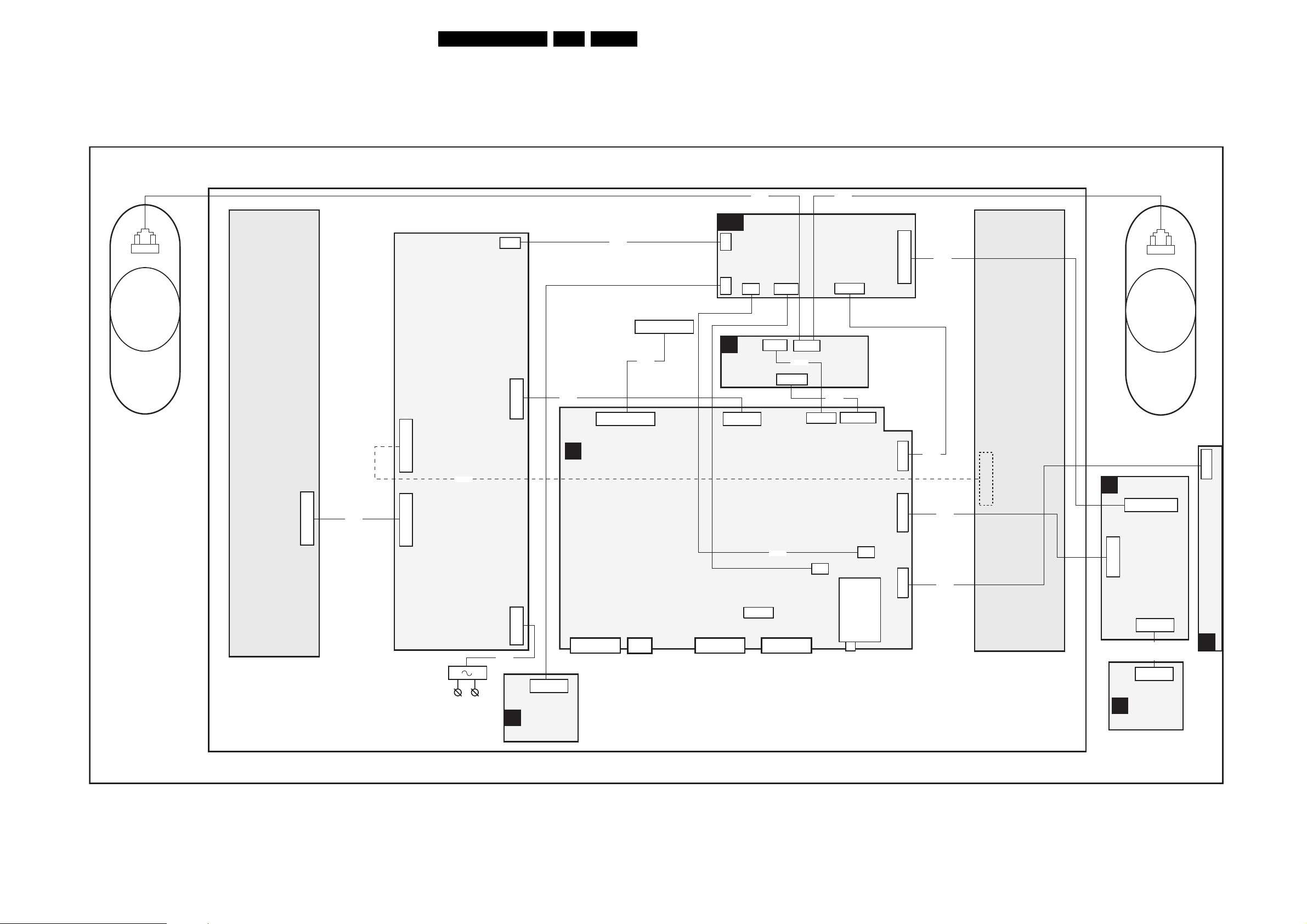
6. Block Diagrams, Test Point Overviews, and Waveforms
Wiring Diagram
WIRING
9LC4.3HE AA 6.
RIGHT
SPEAKER
INVERTER
INVERTER
14P
8520
X530
X520
12P
14P
POWER
SUPPLY
8520
AC POWER
INLET
POWER
IN
8002
3P
X220
X200
12P
X002
2P3
LCD CLOCK
O
(OPTIONAL,
not for NAFTA region)
4P
1442
8903
I-BOARD
HC
8400
LVDS CONNECTION
TO SCREEN
8P06
30P
3P
J10
J2
J1
4P
4P
C
CLASS D
1003
AUDIO
AMPLIFIER
8J02
30P
31P
1P06
SSB
B
Digital A/V Analog A/V Analog A/V
VGA
12P
1J02
3P
1J03
3P
8403
J3
5P
1002
9P
8J03
4P
1001
3P
1J03
1440
5P
8903
J6
8P6
8J04
1JO4(1M52)
TUNER
9P
1103
4P
J4
24P
8407
6P
1K00(1M21)
12P
1K01(1M06)
3P
1K02
8406
8K01
8684
INVERTER
12P
D
12P
J
LEFT
SPEAKER
SIDE AV
1301
24P
1321
1340
5P
5P
1540
IR/LED/LIGHT
SENSOR
8870
3P
KEYBOARD CONTROL
E
1684
F_15820_002.eps
281105
Page 10
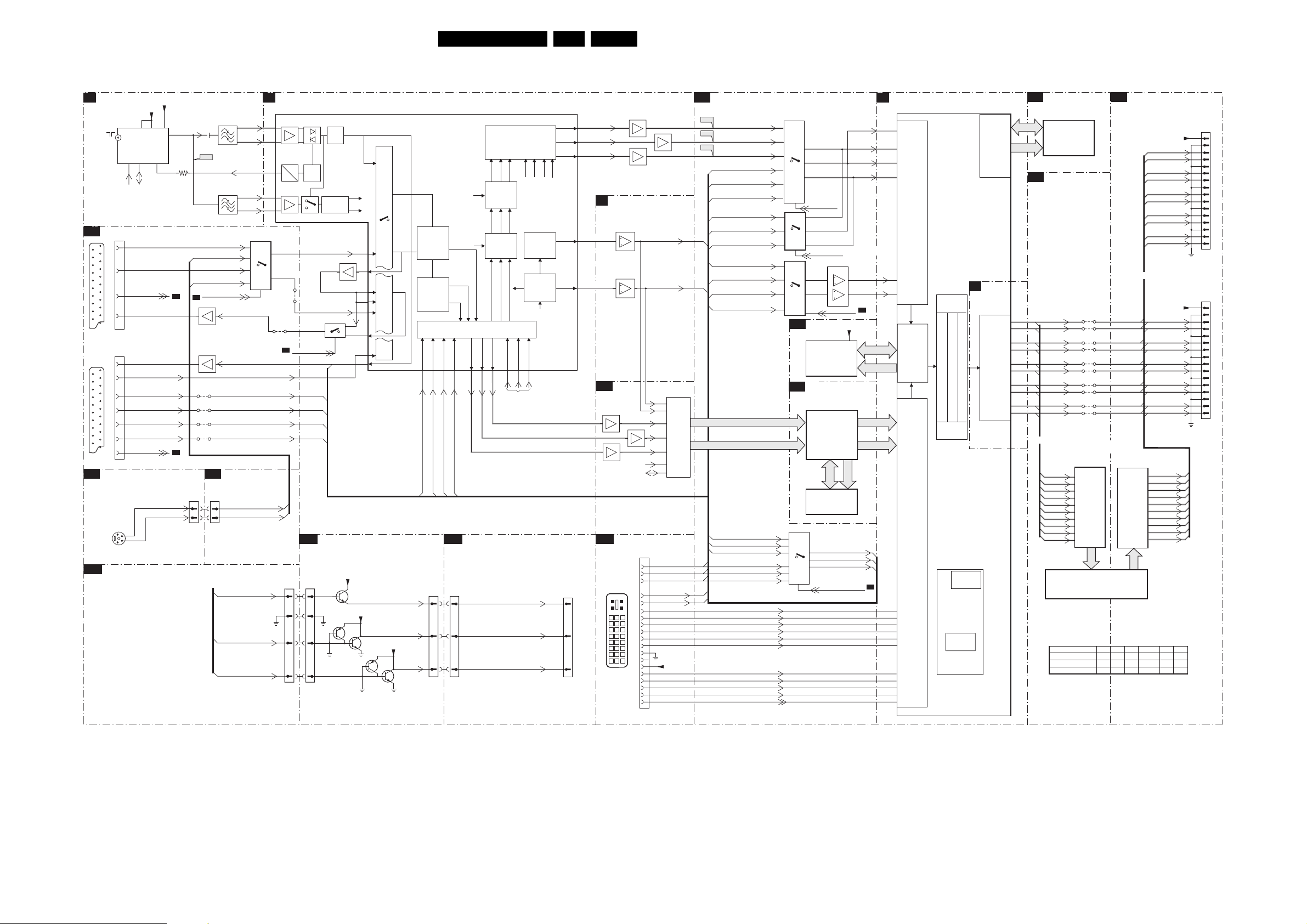
Block Diagrams, Test Point Overviews, and Waveforms
Block Diagram Video
VIDEO
TUNER & VIF
B1
RF
IN
SCART ANALOG IO
B15
1G02
SCART 2
1
21
EXT 2
1G01
SCART 1
1
21
EXT 1
SIDE AV
D
1080
1
5
S-VHS
2
SVHS
SYNC INTERFACE
B3
1102
UV1318S
20
15
8
19
19
20
16
15
11
7
8
+5SW_a
67
TUNER
4
5
SCL
SDA
STATUS_2
SC1_CVBS_IN
STATUS_1
FRONT_YCVBS_IN
3
4
+VTUN
1
SC1_FBL_IN
CVI_Pr_IN
CVI_Y_IN
CVI_Pb_IN
FRONT_C_IN
IF-TER
11
3104
B2
B2
1104
2106
2
F108
1106
2
SC2_Y_IN
FRONT_Y_CVBS_IN
SC2_C_IN
FRONT_C_IN
AV2_DMMI_SW
B2
7G05
EF
7G03
EF
4G14
4G15
4G17
4G16
B17
1K01
1321
2
2
4
4
SC1_CVBS_RF_OUT
B2
B3
B3
B2
7
VIF1
8
VIF2
RF_AGC
SIF1
7
SIF2
8
7G10
2
1
12
13
9
SC2_CVBS_MON_OUT
Present only for
non DVB sets
SC1_CVBS_RF_OUT
SC1_CVBS_IN
SC1_FBL_IN_1
SC1_CV1_DMMI_R_Pr_IN
SC1_CV1_DMMI_G_Y_IN
SC1_CV1_DMMI_B_Pb_IN
SIDE
CONNECTIONS
FRONT_YCVBS_IN
FRONT_C_IN
Hsync_SDTV
Vsync_SDTV
HERCULES
7217
TDA15021H
24
25
31
DC
29
30
14
SC2_AV3_Y_IN
15
4G18
B7
1440
AC
AGC
Detect
SC2_AV3_C_IN
4G13
SC2_OUT_SW
HC
J3
1
1
2
2
3
3
4
4
Sound
Traps
QSS Mixer
AM Demod.
CVBS_COMB
SC2_Y_IN_1
7219
14
B3
B2
B13
B13
B13
I-BOARD
Q10
10LC4.3HE AA 6.
MUX-SYNC INTERFACE
B13
7208
RO
85
G_OSD
Vertical &
East-West
Geometry
Sync Sep
H-OSC
H-Shift
H-Drive
CVBS/Y
B_OSD
RO
GO
BO
Fast Blanking
VDRB
HOUT
GO
86
BO
87
B3
22
VSYNC
HOUT
67
CVBS1
c
cvbs/y
HERCULES
Dig. 2H/4H
Combfilter
Yint
Y Delay Adj.
Chroma
Uint
PAL/NTSC/
SECAM
Decoder &
Vint
Baseband
Delay
RGB/Pr Pb Insert
YUV Interface
INSSW3
R/Pr-3
G/Y3
B/Pb-3
77 78 79 80
SAT
SCAVEM
on text
YOUT
74 75 76 70 71 72
Video
Switch
+
Control
QSS/FM
AM
59
7206
EF
64
51
52
58
13
48
12
9
55
43
UOUT
Skin Tone
U/V Tint
Saturation
Peaking
SCAVEM
U/V Delay
VOUT
RGB Matrix
Blue & Black
Strech
Gamma Corr.
R_OSD
YUV
YUV in/out
H/V
VIN
UIN
YIN
B18
N.C.
INTF_V_OUT
INTF_U_OUT
SC1_R_CVI_Pr_IN
SC1_G_CVI_Y_IN
SC1_B_CVI_Pb_IN
SC1_FBL_IN_1
B15
B13
B13
B13
SIDE AV
D
+5VA
Q2
CVBSTERR
+5VA
Q11
HSYNC
+5VA
Q8
Q9
VSYNC
1301
J4
1
1
2
2
4
4
INTF_Y_OUT
CVBSterr
HSYN
VSYN
1303
9
3
4
TO SMART CARD
EXPRESS BOX
7L01
7L02
B14
CONNECTOR
EF
7209
7210
EF
EF
SYNC INTERFACE
7436-2
Vsync_SDTV
43
7436-1
Hsync_SDTV
21
EF
EF
ADC
7L03
SDA
SCL
7L04
MST9883C
30
31
54
EF
43
48
56
57
DIGITAL IO
1F00
27
26
25
H_PC
28
C5
C3 C4
C1 C2
24
18
916
17
DVI
V_PC
8
1
2
6
7
9
10
11
14
+5VSWI
15
17
18
23
24
16
A/D
CONV.
FE00
FE01
FE02
SC1_R_CVI_Pr_IN
B13
SC1_G_CVI_Y_IN
B13
SC1_B_CVI_Pb_IN
B13
B14
B14
B3,B13
B14
B3
B14
B3,B13
B14
B3
COL_Di(1-7)
COL_YA(1-7)
SC1_CV1_DMMI_R_Pr_IN
B15
SC1_CV1_DMMI_G_Y_IN
B15
SC1_CV1_DMMI_B_Pb_IN
B15
B13
B13
B13
B13
B13
R_SDTV
G_SDTV
B_SDTV
BINA|Pb
GINA|YINA
RINA|Pr
Vsync_SDTV
V_PC
H_PC
Hsync_SDTV
GINA|YINA
RX2-IN
RX2+IN
SCL_DVI
SDA_DVI
RX1-IN
RX1+IN
RX0-IN
RX0+IN
RXC+IN
RXC-IN
HOTPLUG
BINA|Pb
RINA|Pr
27
3
7
25
1
5
11
15
1
1
2
12
13
13
12
7E01
7E02
7E03
1
3
5
2
B10
B19
7E00
R-PR-ADC
17
G-Y-ADC
14
B-PB-ADC
11
I_PC_HD_SEL
9
12
14
2
PC_HD_SEL
19
15
14
10,11
SDRAM
7B01
K4D263238F
1Mx32x4
COLUMBUS
(Dig. PAL/NTC Comb)
7M00
T6TU5XBG
COLUMBUS
DIGITAL COMB
7M01
MSM56V16
512Kx16x2
14
15
4
9
R_PR+
B_PB+
7E04
8
5
4
1
SD_HD_SEL
+2V5_DDR
95
SDRAM
FILTER
COL_D
COL_A
DRAM
SC1_R_CVI_Pr_IN
SC1_G_CVI_Y_IN
SC1_B_CVI_Pb_IN
RGB|CVI_HDA_SEL
G_Y+
AVSY NC
AHSYNC
SOG
PC_HD_DET
B7
FSDATA
FSADDR
COL_Do(1-7)
COL_YB(1-7)
B7
B7
B2,B13
B2,B13
B2,B13
AE10
SCALER
7801
GM1501
C3
D2
C2
B2
L3
L4
B10
A10
N4
N3
B9
A9
B8
A8
AL
B6
ANALOG
INPUT
PORT
FRAME
STORE
CONTROL
DVI/HDMI
INPUT
PORT
SCALER
GRAPHIC
ZOOM
OUT BLENDER
OSD CONTROLLER
BRIGHTNESS/CONTRAST/HUE/SAT
VIDEO
ZOOM
UART
INTERFACE
MICRO
CONTROLLER
INTERNAL
RAM
B9
EXTERNAL
ROM
INTERFACE
SCALER
DISPLAY
TIMING
GEN.
OCMADDR
AE16
AF16
AE15
AF15
AE14
AF14
AF12
AF11
AF13
AE12
B11
OCMDATA
B20
FLASH/CONTROL
7C00
MX29LV040QC
FLASH
ROM
512Kx8
EPLD
TXB0TXB0+
TXB1TXB1+
TXB2TXB2+
TXB3TXB3+
TXBCTXBC+
OR
TXB0+
TXB0TXB1+
TXB1TXB2+
TXB2TXB3+
TXB3TXBC+
TXBC-
7N02
EP1C12F256C8N
4N03
4N01
4N07
4N05
4N11
4N09
4N15
4N13
4N19
4N17
Only for sets with
PIXEL PLUS
7N04
THC63LVDF84B
LVDS
INTERFACE
RECEIVER
RGB
EPLD
PIXEL+
PROCESSOR
SD_HD_SEL H H H H H H
PC_HD_DET H H H H L H
RGB|CVI_HDA_SEL L H L L L L
EPLD
B21
LVDSAn
LVDSAp
LVDSBn
LVDSBp
LVDSCn
LVDSCp
LVDSDn
LVDSDp
LVDSCLKn
LVDSCLKp
7P02
THC63LVDM83R
LVD S
TRANSMITTER
RGB
OR
LVDS_VCC
LVDSALVDSA+
LVDSBLVDSB+
LVDSCLVDSC+
LVDSD-
LVDSD+
LVDSCLK-
LVDSCLK+
LVDS_VCC
LVDSALVDSA+
LVDSBLVDSB+
LVDSCLVDSC+
LVDSDLVDSD+
LVDSCLK-
LVDSCLK+
LVDSAn
LVDSAp
LVDSBn
LVDSBp
LVDSCn
LVDSCp
LVDSDn
LVDSDp
LVDSCLKn
LVDSCLKp
1P07
1P06
HDPCSide-AVEXT2EXT1TV
F_15800_016.eps
1
11
12
13
14
15
16
17
18
19
20
24
25
26
21
22
1
11
10
12
14
13
15
19
18
20
27
26
28
22
21
23
281105
TO DISPLAY (LC4.8 LC4.9)TO DISPLAY (LC4.3)
Page 11
Block Diagrams, Test Point Overviews, and Waveforms
Block Diagram Audio
AUDIO
TUNER & IF
B1
1102
UV1318S(D)
RF IN
SCART ANALOG IO
B15
1G01
1
21
EXT 1
SCART 1
1G02
1
21
EXT 2
SCART 2
SIDE AV
D
1376
AUDIO
IN
DIGITAL IO
B14
PC
AUDIO
IN
1F01
6
2
6
2
IFOUT
TUNER
4
5
SCL
SDA
SC1_COMP_AV1_L_IN
SC1_COMP_AV1_R_IN
L_FRONT_IN
R_FRONT_IN
2
2
4
3
7
11
SEL_IF_SDM
B2
SC2_L_IN
SC2_R_IN
F108
IF-TER
7101
2106
6104
1321
4110
2
3
4G11
4G12
B17
1K01
(1M06)
66
88
1106
7
8
SC1_COMP_AV1_L_IN
SC1_COMP_AV1_R_IN
SIDE CONNECTORS
FRONT_L_IN
FRONT_R_IN
SIF1
SIF2
SC2_L_IN
SC2_R_IN
AudioIN2L
AudioIN2R
HERCULES
B2
7217
TDA15021H
29
30
33
34
35
56
57
49
50
53
54
AD Conv.
Std Stereo
Decoder
AUDIO
SELECT
ADC/DAC
QSS Mixer
AM Demod.
AM
QSS/FM
I2S
Processor
AUDIO
CONTROL
Vol/Treb/
Bass
Features
DACs
11LC4.3HE AA 6.
D
1321
7001
TDA8931T
COMPARATOR
7
4
IN+
7000
TDA8931T
COMPARATOR
7
4
IN+
SIDE AV
HEAD_PH_L
HEAD_PH_R
1G02-1
3
1
1G01-1
3
1
POWER
POWER
OUT
HVPI
OUT
HVPI
7307
TDA1517ATW
2
6
1
21
EXT 2
SCART 2
1
21
EXT 1
SCART 1
1F01
1001
4
3
2
1
RIGHT
SPEAKER
LEFT
SPEAKER
BATHROOM
SPEAKER
16
13
16
13
5007
5006
5306
1
5305
7
AUDIO PROCESSING
B5
4211
61
60
62
63
36
37
4212
AUDOUTLSR
AUDOUTLSL
OUT_MUTE
OUT_MUTE
SOUND-ENABLE
2
6
7602
74HC08PW
3
6
8
7202
MUTE
7201
MUTE
7601
TS482ID
OUT_MUTE
2
&
1
&
5
9
&
10
B16
1J04
1
7
7606
MUTE
HP_DET_R_DC_1
SOUND_ENABLE
POWER_DOWN
EXT_MUTE
SC2_L_MON_OUT
SC2_R_MON_OUT
SC2_L
SC2_R
SC1_L_RF_OUT
SC1_R_RF_OUT
SC1_L
SC1_R
AUDIO AMPLIFIER
C
(CLASS-D)
1002
33
11
88
B17
HP_DET_R_DC_1
B2
B16
B2
B15
AUDIO-R
AUDIO-L
SOUND-ENABLE
7004
INVERTER
SIDE
CONNECTORS
1K01
HP_LOUT
HP_ROUT
10 10
12 12
11 11
SCART ANALOGUE IO
SC2_L_MON_OUT
SC2_R_MON_OUT
SC1_L_RF_OUT
SC1_R_RF_OUT
PHASE
CONTROL
IR LED PANEL
J
6541
GND
7542
VS
OUT
+5VA
6540B
6540A
Green
Red
7540
3544
7541
3540
PC-TV-LED
IR
+5VA
LED-SEL
D
1540
44
55
22
33
11
SIDE I/O +
CONTROL
To Smart Card
Express Box
1340
RC_IR
RD_GR_LED
LED_CTRL
1302
LEDIN_CLK
1
IRIN_DATA-IN
2
3
MODE
4
STATUS_DATA - OUT
GND
5
6
IR_OUT
+5V
LEDIN_CLK
IRIN_DATA-IN
MODE
STATUS_DATA - OUT
GND
IR_OUT
LED_CTRL
RD_GR_LED
RC_IR
+5V
HC
1301
11
22
33
44
55
66
17 17
20 20
21 21
22 22
23 23
I-BOARD
J4
LEDIN_CLK_TXD_SCL1
IR_IN_DATA-IN_RXD_SDA1
MODE
STATUS_DATA_OUT
IR_OUT
PC_TV_LED_OUT
LED_SEL_OUT
RC_IR
U5
P89C664
9
18
MICRO
13
CONTR.
11
1
10
40
+5V
CONTR.
See Blockdiagram
I²C
PC_TV_LED
+3V3STBY
LED-SEL
IR_IN_TV
LIGHT-SENSOR
15
4
4
U4
HEF4053BT
MULTI
PLEX
U3
HEF4053BT
MULTI
PLEX
B17
1K00
J6
66
55
44
33
22
71
B3
E
Channel+
ChannelVolume+
Volume-
Powe r
SIDE CONNECTORS
+3V3STBY
SYNC INTERFACE
+3V3STBY
+5VSW
PC-TV-LED
LED-SEL
3431
6430
KEYBOARD CONTROL
1309
KB
1310
1311
1312
1313
Menu
1314
7430
1684
LIGHT-SENSOR
1K02
22
KEYBOARD
HERCULES
B2
7217
TDA15021H
SEL_IF_SDM
114
107
HERCULES
IR
97
115
120
116
119
102
111
122
127
10
11
4204
4205
SERVICE
SMD
STATUS_1
STATUS_2
EXT_MUTE
SOUND-ENABLE
SC_STANDBY
AV2 _DMMI_SW
1202
B15
B1
B3
B3
B5
B5
B6
B15
F_15800_017.eps
260906
Page 12
Block Diagrams, Test Point Overviews, and Waveforms
Testpoint Overview Small Signal Board
F101 C1
F102 D2
F103 C1
F104 D2
F105 D1
F106 D2
F107 C1
F108 C2
F109 C2
F110 B2
F111 B2
F112 B2
F113 B2
F114 C2
F115 D2
F116 D2
F117 D2
F201 A2
F202 A2
F203 A2
F204 B3
F205 B2
F206 B2
F207 B2
F208 B2
F209 B2
F210 C2
F211 A2
F212 A2
F213 A2
F214 A2
F215 A2
F216 B3
F218 A2
F219 A2
F220 A3
F221 A3
F222 B2
F223 B2
F224 A2
F225 A3
F226 A3
F227 C3
F228 A3
F229 B2
F230 A3
F231 A2
F232 B3
SERVICE TESTPOINTS
F233 B3
F234 B3
F235 B3
F236 C3
F237 B2
F238 B2
F239 B2
F240 B2
F241 B3
F242 B2
F243 B2
F244 B2
F245 A2
F246 B2
F247 A2
F248 B2
I618
F103
I602
F249 B2
F250 B3
F501 A2
F502 A2
F503 A2
F504 A2
F505 A3
F601 A1
F602 A2
F603 A1
F604 A2
F605 A2
F700 A6
F701 A5
F710 A5
F736 A3
I603
F604
F108
F102
F737 A3
F738 A3
F743 B3
F754 A5
F755 A6
F800 B7
F801 B6
F802 C5
F803 B5
F804 B5
F900 C5
F901 C5
F902 C6
F903 C5
F904 C6
F905 B6
F605
F503
F104
F906 B6
F907 B5
F908 C5
F909 C5
F910 C6
FB01 B7
FC00 B5
FC01 B5
FC02 B5
FC03 B5
FC04 B5
FC05 C5
FC06 B5
FC07 B4
FC08 B5
FC09 B5
3139 123 6093 .1
FC10 B4
FD00 C7
FD01 D7
FD02 D7
FD03 D7
FD04 C7
FD05 C6
FD06 C6
FD07 C7
FD08 C7
FD09 C7
FD10 C7
FD11 D7
FD12 C7
FD13 C7
FD14 C7
F504
FD15 C7
FD16 C7
FD17 B6
FE00 C5
FE01 C5
FE02 C4
FE03 B5
FE04 D5
FE05 C5
FE06 D5
FE07 B7
FE08 C4
FE09 C5
FE10 C4
FE11 C5
FE12 C5
I298
FE13 C5
FF00 D6
FF01 D6
FF02 D4
FF03 D7
FF04 D7
FF05 D7
FF06 D6
FF07 D6
FF08 D3
FF09 D7
FF10 D6
FF11 D6
FF12 D6
FF13 D6
FG00 D4
F220
F221
I218
FG01 D4
FG02 D3
FG03 D4
FG04 D3
FG05 D3
FG06 D3
FG07 D3
FG08 D3
FG09 D3
FG10 D2
FG11 D3
FG12 D2
FG13 D2
FG14 D6
FG15 D5
FG16 D6
F736
F737
F738
FG17 D6
FG18 D5
FG19 D5
FG20 D5
FG21 D5
FG22 D5
FG23 D4
FG24 D3
FG25 D3
FG26 D5
FG27 D5
FG28 D5
FG30 D5
FG32 D3
FG33 D3
FG34 D3
I733
FG35 D3
FG36 D4
FG37 D3
FG38 D3
FG39 D4
FG40 D7
FG41 D3
FG42 D4
FG43 D4
FG44 D4
FG45 D4
FG47 D4
FG48 D4
FG49 D4
FG50 D4
FG51 C2
FG53 D4
FG54 D4
FG56 D4
FJ00 A7
FJ01 A5
FJ02 A4
FJ03 A5
FJ04 A5
FJ05 A4
FJ06 A4
FJ07 A5
FJ08 A4
FJ09 A2
FJ10 A2
FJ11 A4
FJ12 A2
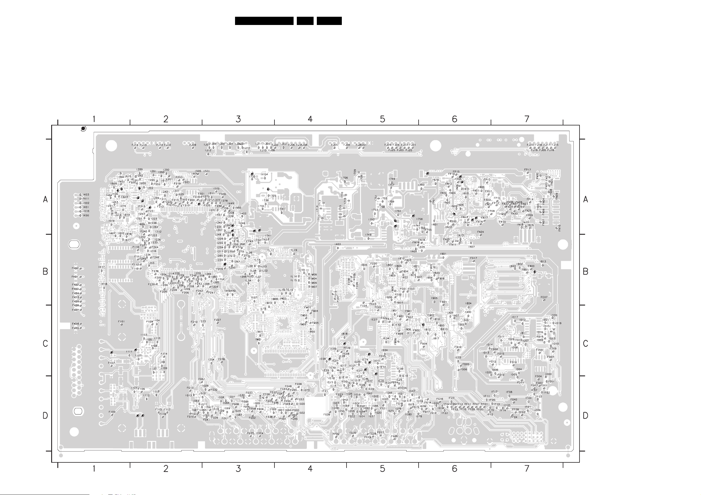
12LC4.3HE AA 6.
FJ13 A2
FJ14 A2
FJ15 A7
FJ16 A7
FJ17 A7
FJ18 A7
FJ19 A7
FJ20 A7
FJ21 A5
FJ22 A5
FJ23 A5
FJ24 A5
FJ25 A5
FJ26 A5
FK00 B1
FK01 B1
FE10
FK02 B1
FK03 B1
FK04 B1
FK05 B1
FK06 B1
FK07 C1
FK08 C1
FK09 C1
FK10 B1
FK11 A1
FM01 C4
FM02 C4
FM03 C4
FM04 C4
FM05 C4
FN01 A6
FE02
FN02 A6
FN03 A6
FN04 A7
FN05 A7
FN06 A7
FN07 A7
FN08 A7
FN09 A7
FN10 A7
FN11 B6
FN12 A6
FN13 A6
FN14 A6
FN15 A6
FN16 A6
FN17 A6
FE12
FE13
FE01
FE00
FN18 B6
FN19 B5
FN20 A7
FN21 A7
FN22 A7
FN23 A7
FN24 A6
FN25 B6
FN26 A7
FN27 A7
FN28 A7
FN29 A7
FN30 A7
FN31 A7
FN32 A7
FN33 A7
FN34 A7
FN35 A7
FP01 A6
FP02 A6
FP03 A6
FP04 A6
FP05 A6
FP06 A6
FP07 A6
FP08 A7
FP09 A7
FP10 A7
FP11 A7
FP12 A7
FP13 A6
FP14 A7
F710
F754
F701
FP15 A6
FP16 A6
FP17 A7
I101 D2
I102 C2
I103 C2
I104 C2
I105 C2
I106 C2
I107 C2
I108 C2
I109 C2
I110 C2
I111 C1
I112 D2
I113 D2
F700
I902
I201 A2
I202 A2
I203 B2
I204 B2
I205 B2
I206 B2
I207 B2
I208 B2
I209 B2
I210 A3
I211 A3
I212 A3
I213 A2
I214 B2
I215 A2
I216 B2
I217 B3
I218 A3
I219 B3
I220 B3
I221 A2
I222 A2
I223 A2
I224 A3
I225 A2
I226 B2
I227 B2
I228 B3
I229 B2
I230 A3
I231 B2
I232 A2
FP02
FP05
FP04
I233 B2
I234 B2
I235 B2
I236 B2
I237 B2
I238 A2
I239 A3
I240 A3
I241 A2
I242 A2
I243 A3
I244 B3
I246 A3
I247 A3
I248 A3
I254 C3
FN14
FN15
I255 B3
I256 B3
I257 B3
I258 B2
I259 B3
I262 B2
I264 A2
I265 B3
I266 B3
I267 B3
I268 B3
I269 A2
I270 B3
I271 A3
I272 B3
I273 C3
I274 A1
I275 A3
I277 A3
I278 A3
I283 B3
I284 B3
I285 B3
I288 B3
I289 A2
I290 A2
I291 A2
I292 A2
I293 A2
I294 A2
I297 A1
I298 B3
I430 A1
I440 B3
I443 B3
I449 A3
I450 A3
I451 A3
I452 A3
I453 A1
I454 A1
I501 A3
I502 A3
I503 A2
I504 A2
I505 A2
I602 A1
I603 A2
I900
I604 A1
I605 A2
I606 A2
I607 A1
I608 A1
I610 A1
I611 B1
I612 A1
I613 A1
I614 A1
I615 A1
I616 A1
I617 A2
I618 A1
I619 A1
I705 A3
F_15270_036.eps
I706 A4
I708 A5
I709 A5
I710 A4
I711 A4
I712 A4
I713 A4
I714 A4
I715 A4
I716 A4
I731 A4
I732 A3
I733 A3
I734 A3
I735 A3
I736 A3
250505
I740 B3
I741 B3
I742 B3
I747 A5
I748 A5
I749 A5
I750 A6
I751 A5
I752 A5
I753 A5
I754 A5
I755 A5
I756 A6
I757 A5
I758 A5
I759 A5
I760 A6
I800 C6
I801 C5
I802 B5
I803 B5
I804 B6
I805 B5
I806 B5
I807 B5
I808 B5
I809 B5
I810 B5
I811 C7
I812 C6
I813 B7
I815 C6
I816 C6
I817 C6
I818 C4
I819 B5
I820 B6
I821 B5
I822 B5
I900 B7
I901 B6
I902 C6
I903 C6
I904 B6
I905 B6
I906 C5
IA00 C6
IA03 B4
IA05 C6
IA06 C6
IA07 C6
IA08 B5
IA09 B6
IB02 B7
IB03 B7
ID00 C7
ID01 D7
ID02 C7
ID03 C7
ID04 C7
ID05 C7
ID06 C7
ID07 C7
ID08 C7
ID09 C7
ID10 C7
ID11 C7
ID12 C7
ID13 C6
ID14 C6
ID15 C7
ID16 C7
ID17 C7
ID18 C7
ID19 C7
ID20 C7
ID21 C7
ID22 C6
IE00 D4
IE01 C4
IE02 D5
IE03 C6
IE04 C5
IE05 C5
IE06 C4
IE07 C4
IE08 C4
IE09 C5
IE10 C5
IE11 C5
IE12 C5
IE13 D5
IE14 D4
IE15 D4
IE16 C4
IE17 C4
IE18 C4
IE19 D5
IE20 D5
IE21 D5
IE22 D5
IE23 C5
IE24 C5
IE25 D5
IE26 D5
IE27 C5
IE28 C4
IE29 C4
IE30 C4
IE31 C5
IE32 C5
IE33 C5
IE34 C5
IE35 D5
IE36 C5
IE37 C5
IF00 D7
IF01 D7
IF02 D7
IF03 D7
IF04 D6
IF05 D6
IF06 D7
IF07 D7
IF08 D7
IF11 D6
IF12 D6
IF13 D7
IF14 D7
IF15 D6
IF17 D7
IF20 D7
IF21 D4
IF22 D6
IF23 D6
IG00 D4
IG01 D4
IG02 D4
IG03 D4
IG04 D3
IG05 D3
IG06 D3
IG07 D3
IG08 D3
IG09 D3
IG10 D3
IG11 D3
IG12 D3
IG13 D2
IG14 D6
IG15 D5
IG16 D6
IG17 D5
IG18 D6
IG19 D5
IG20 D6
IG21 D5
IG23 D5
IG24 D5
IG25 D5
IG26 D5
IG27 D4
IG28 D3
IG29 D3
IG30 D3
IG40 D5
IG42 D5
IG43 D4
IG46 D5
IG47 D5
IG49 D4
IG50 D4
IG52 D5
IG53 D5
IG54 D5
IG55 D5
IG56 D5
IG57 D5
IG58 D5
IG59 D4
IG60 D3
IG61 D2
IG62 D2
IG63 D3
IG64 D3
IG67 D3
IG69 D3
IG73 D4
IG75 D5
IG76 D6
IG78 D5
IG79 D5
IG80 D5
IJ01 A3
IJ02 A3
IJ03 A4
IJ04 A3
IJ05 A3
IJ06 A3
IJ07 A3
IJ08 A3
IJ09 A3
IJ10 A3
IJ11 A3
IJ12 A3
IJ13 A3
IK00 A1
IK01 A1
IK02 A1
IK03 A1
IK16 A1
IK17 B1
IK18 B1
IL01 B3
IL02 B3
IL03 B3
IL04 B3
IL05 B3
IL06 B3
IL07 B3
IL08 B3
IL09 B3
IL10 B4
IL11 B4
IL12 B4
IL13 B4
IL14 B4
IL15 B4
IL16 C3
IL17 B3
IL18 B3
IL19 B4
IM00 C4
IM01 C3
IM03 B4
IM04 B4
IM06 B4
IM07 B4
IM08 B4
IM09 B4
IM10 B3
IM11 C3
IN01 A6
IN02 A6
IN03 A6
IN04 A6
IN05 A6
IN06 A6
IN07 B6
IN08 A6
IN09 A6
IN10 A6
IN11 A6
IN12 A6
IN13 B6
IN14 A6
IN15 B6
IN16 A7
IN17 A7
IN18 A7
IN19 A6
Page 13

Block Diagrams, Test Point Overviews, and Waveforms
I2C IC Overview
13LC4.3HE AA 6.
I²C
HERCULES
B2
7217
TDA15021H
HERCULES
PROCESSOR
SET
109
108
104
112
113
+3V3STBY
3232
3233
ERR
6
+3V3STBY
NVM_WP_HERC
B15
ERR
17
B14
CONNECTOR
3249
SCART ANALOGUE IO
DIGITAL IO
C5
C3 C4
C1 C2
1F00
24
18
916
17
DVI -D
1802
2
1
JTAG
I2C
7
SW_I2C_SDA
SW_I2C_SCL
7
6
JTAG_TDI_SDA
JTAG_CLK_SCL
5 6
7207
M24C16
EEPROM
NVM
ERR
9
DCC_5V
3F18
5 6
7F03
M24C02
EEPROM
256x8
3F17
SDA
SCL
1G03
Reserved
For DMMI
SDA_DVI
SCL_DVI
1
2
3838
+3V3IO
3837
B8
SCALER
N3
N4
AF7
AD6
N1 N2
7801
GM1501H
SCALER
ERR
4
ADDRESS
DATA
ADDRESS
DATA
SCALER
B7
M1
M2
3818
P3
P4
NVM_WP_SCALER
AF5
+3V3SW
OCMADDR
FSADDR
FSDATA
3817
OCMDATA
TUNER & IF
B1
3102
(5108)
UART_TX
UART_RX
FLASH / CONTROL
B11
SDRAM
B10
3101
5 4
1102
UV1318S
TUNER
ERR
10
(5107)
3122
3123
SDA_IO
SCL_IO
56
7C01
M24C32
7
EEPROM
ERR
7C00
MX29LV040
FLASH ROM
7B01
K4D263238F
SDRAM
ERR
3125
8
14
3124
SDA
SCL
SERVICE
CONNECTOR
COMPAIR
1107
SERVICE
CONNECTOR
UART
1101
HC
I-BOARD
+5VD
1103
J2
33
22
COLUMBUS
B19
3M14
3M15
A15 B15
1
2
3
1
2
3
7M00
T6TU5XBG
COLUMBUS
CTRL
ERR
11
SCALER INTERFACE
B9
7A00
PCA9515ADP
3
2
B18
RES
4A01
4A00
FOR
PDP ONLY
ADC
7L07
+3V3SWB
6
7
7L06
+3V3SWB
3L36
B21
DISPLAY
EPLD
1P07
(1G50)
31
30
TO
3L37
3L19
MST9883C
INTERFACE
3L20
57 56
7L04
ANALOG
ERR
7
B20
EPLD
4N21
4N22
+5VD
RP5
R35
56
U8
MC24C16
T2 R2
7N02
EP1C12F256C8N
EPLD
BANK 4
ERR
16
RP5
R34
SDA1
SCL1
3N47
3N46
R26
R25
CONTROLLER
24
25
+3V3SW
1N02
1
2
SDA
3
4
SCL
FOR
DEVELOPMENT
USE ONLY
32
U5
P89C664
8 bit
MICRO
SDA2
22
21
SCL2
23
SDA3
+5VD
RP1
7
5
CLK_LED-IN_SCL
43
DATA-IN_SDA1
44
RP1
TXD
RXD
TXD
RXD
R24
R39
+5VD
R69
Q12
R23
+5VD
13
11
12
12
2
13
3
R40
U3
HEF4053BT
MULTI
PLEXER
U7
ST202ECD
RS232
TRANCIEVER
U2
HEF4053BT
MULTIPLEX.
14
14
13
IR-IN_DATA-IN_
15
LEDIN_CLK_
14
R67
R68
TXD232
RXD232
RXD_SDA1
TXD_SCL1
J1
2
3
J4
24
10
11
2
1
TO
CLOCK MODULE
(Optional)
SIDE I/O
D
1301
SDA3_IR-OUT
24
10
TXD232
11
RXD232
2
IR-IN_DATA-IN
1
LEDIN_CLK
1303
7
5
6
1302
2
1
F_15800_019.eps
281105
EXPRESS BOX
TO SMART CARD
EXPRESS BOX
TO SMART CARD
Page 14

Block Diagrams, Test Point Overviews, and Waveforms
Supply Voltage Overview
SUPPLY LINE OVERVIEW
SUPPLY
PANEL
(PSU)
X200
X220
X002
TOP CONNECTORS
B16
1J02
1
2
3
4
5
6
7
8
9
POWER_DOWN
STANDBY
10
BACKLIGHT_CTRL
11
LAMP_ON_OFF
12
1J01
(1M46)
1
2
3
N.C
.
1J07
4
5
N.C
.
6
1J08
7
8
N.C
.
9
10
N.C
.
4J01
11
RES
1J01
(1M03)
BACKLIGHT_CTRL
1
2
N.C
.
LAMP_ON_OFF
3
4
5
FAN_SPEED
6
N.C
.
STANDBY
7
PROTECT_AUD
8
9
N.C
.
10
POWER_UP_OK
RES
TO J10
HC
I-BOARD
MFD SUPPY
UFD SUPPY
+12VUFD
+5V_UFD
UFD CONTROL
14LC4.3HE AA 6.
TUNER & IF
B1
7758
5753
5754
5733
5700
+5VSW
+5VSW_a
+5VSW_b
+3V3STBY
+3V3STBY
+1V8_A
+1V8_B
HERCULES
+5VSW
+8VSW_TV
+3V3STBY
+3V3SW
+5VSW
+5VSWI
+5VD
+3V3SW
+3V3STBY
+5VSW
+5V
+12VUNREG
+12VSW
+8VSW_TV
+5VSWI
6735
+VTUN
+5VSW
5737
(Only LCD)
PAN_VCC
LVD S_VCC
(Only UFD)
+5V
+3V3STBY
+3V3SW
1103
B8
B8
1
B6
J2
HC
B8
B8
B6
B16
B16
B6
N.C.
B8
B8
B2
B6
B4,B9,B13,
B14,B19
B6
B22
B1,B2,B3,
B15,B17
B6
B21
B6
B6
B3,B5,B7,
B8,B9,B11
B12,B13,
B19,B20,
B21
B6
B6
1J03
VP
+3V3STBY
+12VUNREG
5J03
5J04
B9
B8
B8
B9
B7
+5V
1003
1
C
B1,B3,B3,
B5,B6,B9,
B17
B6
N.C.
B16
B16
B6
B6
B16
B6
B6
B6
B6
B16
B6
N.C.
B16
N.C.
B16
+5VSW
5102
5103
+3V3STBY
HERCULES
B2
+3V3STBY
3265
7215
3264
7216-1
3263
7217
3262
7216-2
+5VSW
+8VSW_TV
SYNC INTERFACE
B3
+3V3STBY
+3V3SW
+5VSW
AUDIO DELAY LINE (RESERVED)
B4
+5VSWI
5501
AUDIO PROCESSING
B5
+3V3SW
+3V3STBY
+5VSW
(Only UFD)
+5V
DC-DC CONVERTER
B6
+12VUNREG
7738
5738
IN OUT
7752
5752
DC/DC
5730
7754
5712
COM
7708
IN OUT
COM
SC_STANDBY
Converter
7730
5757
+5V
+3V3STBY
6708
5709
7710
IN OUT
OR
5704
OR
COM
PWR
REG
PANEL-PWR-CTL
SCALER
B7
+1V8_CORE
+2V5_DDR
+3V3SW
+3V3_IO
+3V3_PLL
SCALER
B8
+3V3SW
5900
5901
5902
5903
5904
5905
5906
5907
7900
IN OUT
COM
7901
IN OUT
COM
SCALER INTERFACE
B9
+3V3SW
+3V3STBY
+5VSWI
DVI
+5V
B10
+2V5_DDR
B11
+3V3_IO
+3V3SW
B12
+3V3SW
+5VHDMI
B13
+3V3SW
+5VSWI
B14
+5VSWI
1F00
1
B15
+5VSW
(ONLY UFD)
SDRAM
3B01
FLASH / CONTROL
HDMI (Not for EUR Sets)
MUX-SYNC INTERFACE
DIGITAL IO (Only for EUR Sets)
6F00
6F01
3F20
SCART ANALOGUE IO (Only for EUR Sets)
5908
5909
5910
5911
5F03
+1V8_CORE
+2V5_DDR
+3V3SW
+3V3_IO
+3V3_PLL
+3V3SW
3V3_PLL
3V3_ADC
3V3_DVI
3V3_IO
3V3_LBADC
3V3_LVDSA
3V3_LVDSB
3V3_LVDS
+2V5_DDR
+1V8
+1V8_ADC
+1V8_DV1
+1V8_CORE
+3V3SW
+3V3STBY
+5VSWI
+5V
+2V5_DDR
FSVREF
+3V3_IO
+3V3SW
+3V3SW
+5VHDMI
+3V3SW
+5VSWI
+5VSWI
DDC_5V
DVI_5V
+5VSW
1J03
B16
HC
B16
B19
J4
B6
B6
B6
B8
B6
B6
B6
B6
B6
B7
B7,
B11,B20
B7,B10
B7
HDMI
VGA
SIDE CONNECTORS
B17
+3V3STBY
5K00
+5VSW
5K01
ADC
B18
+5VSWIA
7K05
IN OUT
COM
COLUMBUS
B19
+3V3SW
5M03
+5VSWI
5M04
EPLD
B20
+3V3SW
+3V3-IO
EPLD
B21
+3V3SW
5P01
7P01
IN OUT
COM
LVDS_VCC
DIGITAL IO (Not for EUR Sets)
B22
1Q03
18
1870
9
10
+5VSWI
B23
+5VSW
C
1003
3
D
1301
7
21
6Q16
3Q16
3Q17
5Q16
3Q18
CINCH ANALOGUE (Not for EUR Sets)
CLASS D AUDIO AMPLIFIER
5001
SIDE I/O + CONTROL
+3V3STBY_1
+5VSW_1
5P02
5P03
3001
+3V3STBY
+5VSW
+5VSWIA
+3V3SWB
+3V3SW
+3V3SWA
+5VSWI
+5VSWIA
+3V3SW
+3V3-IO
+3V3SW
+3V3-IO
1V5
1V5-PLL
1V5-INT
LVDS_VCC
+5VSW
DDC_5V
+5VSWI
+5VSW
VP
VP_SGN
+12V+12V
+5V+5V
+5V
1K00
1K01
1340
1540
5
7
2
1103
B1
X220
PSU
1340
D
J1
HC
1304
B18
B12
1540
J
D
J
I-BOARD
HC
J2
+3V3STBY
1
L1
J10
+12V
1
IR LED
J
1540
2
CLOCK BOARD (OPTIONAL)
O
1442
1
U1
SMPS
CONTR
L1
+3V3STBY
+3V3
D2
+5V
L4
J1
1442
1
O
+5VA
L5
+5VD
L6
+5V
+12V
+5VA+5VA
VDDVDD
J4
21
7
F_15820_001.eps
1301
D
281105
Page 15

Circuit Diagrams and PWB Layouts
7. Circuit Diagrams and PWB Layouts
Side I/O Panel
SIDE I/O (26” & 32” only)
D
10R
3302
2311
3304
75R
7301
BC857B
+5V+5V
RES
3303
2303
RES
3342
10K
32
D
C
B
1305
SVHS
6
1376
AV1
LGT1509-0200
3340
100K
3339
47R
1
GND
3
Y_in
4
C_in
2
GND
GND
Shiel d5GND
7
1
4
3
2
1
23
3338
100R
32
S301GAP
7304
BC857BW
7303
BC847BW
1
S30 4
GAP
S30 5
GAP
S302GAP
S30 3
GAP
2305
RES
3337
1K
3301
75R
+5VSW1
2310
1uF
3309
75R
4
6
5
6301
BZA4 08 B
1
3
2
3305
3307
100K
1K0
2
1
3
3310
56K
3306
15K
2306
330pF
3308
15K
2307
330pF
3341
10K
7305
1
7302
BC847BW
1
2347
1uF
3335
100K
BSN2 0
3336
10K
32
10R
1304
TC18-041-03
1306
FishHook Wire
1
1
2302
47pF, EMC
2304
47pF, EMC
1
3
2
A
HIS
HI S.SCH
PHI LIPSL OGO
P
b
LEADFREE
3
11225
3
4
4
6
6
5
5
6633112
4
2
5
4
4301
0R
FRONT _C_IN
FRONT _Y_CVBS_IN
L_FRONT_IN
R_FRONT_IN
2312
2u2
+5VSW1
2341
1uF
1302
6PIN-CONN
1303
10PI N-CONN
1
2
3
4
5
6
3326
33K
1
2
3
4
5
6
7
8
9
10
3325
RES
+12VA
HEAD_PH_ L
HP_DET_R_DC1
HEAD_PH_ R
2342
1uF
3327
33K
3328
RES
RD_GR_L ED
3323
1K
2346
1uF
1
2
3
3331
10K
6309
BZA408B
3324
1K
1
2
3
2316
10uF/16V
6310
BZA408B
10
11
12
+
1
3332
RES
6
5
4
HSYN
VSYN
TXD232
RXD232
SDA 3_I R- OUT
DCM-POR
CVBSterr
GNDA
1321
1
2
3
4
5
6
7
8
9
12PI N-CONN
3320
10K
3333 10K
32
+5VSW1
3343
4K7
2313
1uF
4
6
5
4
TO 1K 01 OF SSBBD
2343
470pF, EMC
7309
BC847BW
7311
1
PBSS5350Z
32
1 24308
JUMPER
+12V
6307
15LC4.3HE AA 7.
654321
+12V
2318
1uF
1311
RXEF0 20
12
34
56
78
910
1112
2319
2u2
+12VA
LIGHT_SENSOR
LED_SEL
1312
R30R16 0
+12VA
5305
6.8u H
+5V
3314
4K7
3
2
+3V3
3329 1K
1314
B4B- PH-SM 3- TB
5306
6.8u H
7313
BC84 7BW
1
1
TP1
2
TP2
3
TP3
4
2340
2n2F
3315
10K
3317
0R
Notice:
1308 connector
Even nos.to SSB
Odd nos. to IRLED
5301 220R
5302 220R
5303 220R
2339
1nF
SDA 3_I R- OUT
IROUT
IRIN_DATA-IN
STA TU S_DA TA -O UT
HSYN
VSYN
DCM-POR
RC_Pull_UP
+5V
2308
100nF
53
4
7312
74HC1G86
1
2
2338
1nF
+12V
3334
10K
S30 9
GAP
2320 100U/16V 10% TAN-D
+
TP4
TP6
S31 0
S31 1
S31 2
GAP
GAP
GAP
GND_USB GND_USB
S30 7
S30 8
GAP
GAP
1309
1
GND
2
SCL_ I 2C
3
SDA _I 2C
4
IRQ_DIGITAL
5
RC_OUT
6
GND
7
DATA_IN
8
DATA_OUT_SDA
9
TVCLK_SCL
10
+12V
11
+12V
12
+12V
13
GND
14
GND
15
GND
16
HSYNC
17
VSYNC
18
POR
19
RC_Pull_UP
20
GND
AF620X- A2G1T
3316
1K
TP5
TP7
S30 6
GAP
3319
2321
270K
2u2
7306
13
Pow er Goo d
3313
560K
2314
1uF
3
18
17
5
+
2309
100uF/16V
6308
BZX384-C5V6
BZX384- C5V6
A K
A K
3322
4K7
+12V
2315
1uF
2317
1uF
7307
TDA1517ATW
IN1+
IN2-
MODE
SVR R
LEDIN_CLK
IRIN_DATA-IN
MODE
STA TU S_DA TA -O UT
GND
IROUT
1
2
3
NIS5102
Ri
Ri
OVLO
UVLO
Enable/ Ti me r
1307
6
5
4
SPPH2
VCC
Curr ent L imi t
NC
GND4NC
8
9
15
VP1
+
-
+
-
Vcc
SGND
4
3
2
1
+5V
3
2
A
B
3330
4K7
Ccharg e
+3V3
Sour ce
16
VP2
PGND10PGND
+5V
7314
BC84 7BW
7
10, 11, 12
6
5
OUT1A
OUT1B
OUT2A
OUT2B
11
RC_Pull_UP
1
3321
10K
470uF/10V
8
9
12
13
1
NC
2
NC
6
NC
7
NC
14
NC
19
NC
20
NC
HS
21
1310
3PIN
1
LED_CTRL
318 0R
3
RD_GR_L ED
RC_IR
3311
10K
3312
10K
3344
10K
2301
3
2
IR_IN
5304
BLM 31PG 12 1SN1L
3345
75R
3346
0R
+
2345
2u2
TO I board
10
11
12
13
14
15
16
17
18
19
20
21
22
23
24
1308
B12B- PHDS S-B
PC_T V_L ED
1301
1
2
3
4
5
6
7
8
9
B24B- PHDS S-B
1
2
3
4
5
1340
5PIN-CONN
RC_IR
1313
1
2
3
4
5 6
1734366-1
4
2
7
1
6
3
5
D
D
1322
TC38-103-01
C
B
A
3139 123 6095.3
123456
G_15801_001.eps
140806
Page 16

Circuit Diagrams and PWB Layouts
Layout Side I/O Panel (Top Side)
16LC4.3HE AA 7.
3139 123 6095.3
Layout Side I/O Panel (Bottom Side)
G_15801_002.eps
170806
3139 123 6095.3
G_15801_003.eps
170806
Page 17

LED and IR Panel
Circuit Diagrams and PWB Layouts
17LC4.3HE AA 7.
D
C
B
J
LED & IR
12
1540
S5B-PHK
6544
SIR-341ST3F
5
4
3
2
1
12
6543
TSML- 1020
3545
220R
3549
Res
IR
LED-SEL
PC- T V - LED
2541
10uF
54321
6
J
D
+5VA
3540
470R
12
6542
TSML- 1020
1
3546
220R
SPR- 3 25M VW
32
1
7543
Res
3544
4K7
+5VA
23
7540
BC857BW-1
32
Green Red
6540B
SPR- 3 25M VW
1
3547
4K7
6540A
32
7542
BC847BW-1
32
BC847BW-1
12
7541
1
+5VA
3548
3542
4K7
220R
6541
3
VS
1
OUT
2
2540
100uF,16V
+
GN D
TSOP34136
C
B
A
3139 123 6097.1
A
F_15800_012.eps
280505
1 2 3 4 56
Page 18

Circuit Diagrams and PWB Layouts
Layout LED and IR Panel (Top Side)
18LC4.3HE AA 7.
Personal Notes:
3139 123 6097.2
Layout LED and IR Panel (Bottom Side)
F_15800_013.eps
281105
3139 123 6097.2
F_15800_014.eps
281105
E_06532_012.eps
131004
Page 19

i-Board Panel
Circuit Diagrams and PWB Layouts
19LC4.3HE AA 7.
654321
D
C
B
A
HC
LCD Clock
To Side
I/O
To TV
BD
5P-CONN-SR-V
To TV
BD
Fr om TV
LC04V
10P- CONN-SR-V
LC04C
8P-CONN-PH-V
J10
1
2
3
3P-CONN-PH-B
J1
4
3
2
1
4P-CONN-T YCO
J7
5
4
3
2
1
5P-CONN-T YCO
J4
1
2
3
4
5
6
7
8
9
10
11
12
13
14
15
16
17
18
19
20
21
22
23
24
24P- CONN-PHDSS-B
SR
J3
1
2
3
4
5
SR
J2
4
3
2
1
4P-CONN-SR-V
J5
SR
1
2
3
4
5
6
7
8
9
10
J6
SR
1
2
3
4
5
6
7
8
i-BOARD
+3V3ST BY+12V +3V3
L1
6u8
R87
NFR254R7
U9 L ED5 0CZ
3
IN
OUT
GND
2
L7 Ferrit ebe ad
C7 100nF
LCM_POW
SCL2
SDA2
LEDIN _CLK_TXD_SCL1
IR-IN_DATA-IN_RXD_SDA1
MODE
STA TU S_DA TA _OUT
GND
IR_OUT
+12V
HSYNC
VSYNC
TXD232
RXD232
DCM_POR
CVBSTER R
GNDA
HP_ROUT_R C-PULL UP
HP_LOUT
KEYBOARD_TV INTP
PEND _IR
PC_T V_L ED_ OUT
L10 6u8 - 1008
LED_SEL_OUT
RC_IR
R70 100R
C8
100nF
R7
100R
1
Q2
BC847BW
R38
220R
GNDA
+3V3ST BY
HP_ROUT_R C-PULL UP
HP_LOUT
PC_T V_L ED
LED_SEL
GND
+3V3S
LI GHT SEN SOR
IR_IN TV
KEYBOARD_TV INTP
P50_IT V
IR_IN TV
LED_SEL
PC_T V_L ED
LI GHT SEN SOR
P50_IT V
+5VA
3
2
HSYN
VSYN
SDA
SCL
R9
220R
+12V
+3V3S
GNDA
+5V
R71
0R
1
R84
0R
+
C1
220uF, 16V
Q14
PBSS5140U
3
2
R73
4K7
+5V
R10 100R
R11 100R
R74 100R
R13 100R
R16 100R
R43
0R
CVBSTER R
R8
68R
HP_ROUT _RC-PULLUP
IR_IN TV
LED_SEL
R49 1 R5
R50
1R5
C38
27pF
R72
1
1K
VSYN
C29
10uF
C39
27pF
3
2
BC847BW
R81 0R
+5VA
Q4
R76
10K
1
+5VA
32
L3
68uH
R2
220R
R4
1K0
SCL2
SDA2
LCM_POW
R75 0R
R18
1K0
R82
10K
1
Q15
BC847BW
+5VD
L6
6.8uH - 1008
+ C6
+5VA
13
12
1
2
3
5
8
7
6
RC_IR
32
D3
SDA3
PEND _IR
Q1
BC847BW
L5
6.8uH - 1008
BZX384-C5V6
TXD
RXD
R27
10K
+5V
Q12
1
BC847BW
R28
10K
+5V
+ C4
220uF, 16V
IR_PUL LUP_SW
L8
6.8uH - 1008
LCM_POW
100uF, 16V
32
U1
MC34063AD
8
Sw it ch
Drive
Coll ecto r
Coll ecto r
IpkSense
7
Sw it ch
Emit t er
6
Vcc
Timing
Capacit or
5
Comparat or
Ground
Inv. I/p
R5
2K7
C40 1nF
+5VA
Q3
BC857BW
1
R15 10K
R17
150R
+5VA
C11 100nF
U3
16
14
Za
Y1a
Vdd
Y0a
15
Zb
Y1b
Y0b
4
Zc
Y1c
Y0c
11
Sa
Vss
10
Sb
Vee
9
Sc
HEF4053BT
R19
10K
32
R83
1K
Q8
BC857BW
1
R51
10K
R85
10K
Q5
BC847BW
1
R52
47K
2
3
R54
10K
+5VA
+5VA
R53
47K
D2
SS24
1
A K
2
C2
3
4
100pF
R6
470R
2
3
13
12
1
RJI R_IN
2
3
Tristate
5
8
7
6
E
R20
10K
1
R48
22K
U4
14
Za
15
Zb
4
Zc
11
Sa
10
Sb
9
Sc
HEF4053BT
R55
4K7
32
Q9
BC847BW
14
15
11
10
R3
100R
R14
2K2
Za
Zb
4
Zc
Sa
Sb
9
Sc
+5VA
16
R12
10K
L4
6.8uH
C28
+ C3
10uF
IRIN _DATA-IN
+5VA
C9
100nF
U2
16
Y1a
Vdd
Y0a
Y1b
Y0b
Y1c
Y0c
Vss
Vee
HEF4053BT
STATUS_DATA_OUT 1
C12 100nF
13
Y1a
Vdd
12
Y0a
1
Y1b
2
Y0b
3
Y1c
5
Y0c
8
Vss
7
Vee
6
E
1
220uF, 16V
E
+
C5
100uF, 16V
R56
10K
R86
10K
BLM21P221SN1D
+C26
+5VD
8
2 7
3 6
1
R1
100R
Q10
BC857BW
1
100uF, 16V
C33
10nF
C34
10nF
L14
C27
100nF
RP1
10K-RP
4 5
R57
47K
23
C13 27pF
C14 27pF
+5VA
R58
47K
R59
10K
SDA1
SCL1
+5VD
C42
100nF
+5VD +5VD
RP2
10K-RP
1 8
2 7
364 5
CLK_ LED- I N_SCL1
DATA-IN_SDA1
LIGHT SENSOR
R25 100R
R26 100R
SCL
SDA
IB_IROUT
TV_POR
R60
4K7
32
Q11
1
BC847BW
SPAREIO
J9
3P-CONN-SR-V
1
C30
10nF
C32 10nF
+5VD
U8
5
SDA
6
SCL
7
WC
8
VCC
MC24C16
2
3
R80
SR
10K
C31
10nF
R77 10K
R23
4K7
R29
2K2
+5VD
C43
1uF
VSS
34
P0.3 /A D3
35
P0.2 /A D2
36
P0.1 /A D1
37
P0.0 /A D0
38
VCC
39
NIC*
40
P1.0 /T 2
41
P1.1 /T 2EX
42
P1.2 /EC I
43
P1.3 /CEX 0
44
P1.4 /CEX 1
E2
E1
E0
1 8
33
R24
4K7
C37
10nF
4
3
2
1
7
6
2
3
P1.5/ CEX 21P1.6/SCL2P1.7/SDA3R
4 5
P0.7/AD730P0.6/AD 631P0.5/AD532P0.4 /A D4
T
S
4
3
2
R63
47K
RP3
10K-RP
29
p
EA/V p
P3.0/ RxD5NIC*
D
X
R
28
NIC*
6
R780R
L13
BLM21P221SN1D
R79 10K
C35 10nF
25
24
26
27
ALE
PSEN
P2.7/ A15
P2.4 /A 12
P2.3 /A 11
P2.2 /A 10
P2.1 /A9
P2.0 /A8
XTAL1
XTAL2
P3.7 /R D
P3.6 /W R
P3.1/T xD7P3.2/INT0
P3.3/I NT19P3.4 /
8
10
RC_IR
TXD
PC_TV _LED
Q6
BC847BW
1
C15
1uF
R64
10K
100nF
23
14
A
6/
.
P2.5/A13
P2
NIC*
VSS
/T0
3
X
CE
P3.5/CEX4/ T1
U5
11
P89C664HBBD
R31
22K
1
C41
Reserve
C18
22
21
20
19
18
17
16
15
14
13
12
C45
10nF
R42
0R
+5V
IB_IROUT
R32
22K
32
Q13
BC847BW
HSYNC
C44 100nF
L12
6u8- 1008
100uF, 16V
TXD232
RXD232
R21
100R
R44
10K
DCM_POR
C22
C19 100nF
C20 100nF
R62 100R
R61 100R
SDA3
R69 10K
R22 1K
X1
16MHz
RXD
TXD
+
C21
100nF
2
V+
6
V-
14
T1_OUT
7
T2_OUT
13
R1_IN
8
R2_IN
+5VD
R33 100R
R34 100R
R35 100R
RP5
1 8
2 7
3 6
4 5
10K-RP
C16 27pF
C17 27pF
+5VD
RP4
4 5
3 6
2 7
1 8
10K-RP
SW1
1 2
Tact Sw itch, SKQNABD010
R30
5K6
16
VCC
R1_OUT
R2_OUT
GND
ST202ECD
15
+5VD
+5VD
U6
DS1813
RST1VCC
D
N
G
3
T1_IN
T2_IN
C1+
C1-
C2+
C2-
+5VD
2
U7
1
3
4
5
11
10
12
9
32
BC847BW
R40
4K7
R36 100R
+5VD
C24 100nF
C23 100nF
R37 100R
J8
1 2
Q7
2P-Shrouded-HDR
1
R46 4 K7
R47
4K7
R39
4K7
R67
100R
R68
100R
L11
6.8uH - 1008
C25
1uF
DGND
C36
1uF
D1
BZX384-C2V7
R41
0R
C46
+
100uF, 16V
STATUS_DATA_OUT 1
LED_SEL_OUT
PC_T V_L ED_ OUT
M2
TXD
RXD
CVBSTER R
VSYNC
SCL1
SDA1
SDA2
SCL2
D
C
B
A
3139 123 6133.3
123456
LED_SEL_OUT
VSY NC
HSYN
F_15800_006.eps
240505
Page 20

Circuit Diagrams and PWB Layouts
Layout i-Board Panel (Top Side)
20LC4.3HE AA 7.
3139 123 6133.3
Layout i-Board Panel (Bottom Side)
F_15800_007.eps
240505
3139 123 6133.3
F_15800_008.eps
240505
Page 21

LCD Clock Panel
Circuit Diagrams and PWB Layouts
21LC4.3HE AA 7.
4321
O
D
C
B
LCD CLOCK PANEL
I/O
VDD
SDA
SCL
VSS
1442I/O
I/O
VDD
SDA
SCL
VSS
RES
1443I/O
1
2
3
4
1
2
3
4
5
SDA
SCL
VSS
R12
C1
100uF
BLM21PG221SN1DL1
R2
100R
R3
R4
100R
100R
VDD
Q4
Q1
BC857B
LED
VDD
C3
10P
0.1uF
C2
10P
R7
100KC4
R1
2K2
R6
10K
J1
1uF
R9
2K2
R10
2K2
15
16
17
18
19
20
21
22
23
24
25
26
27
28
4MHz
Q3
BC857B
U1
PC3
PC4
PD0/PWM0
PD1/PWM1
/RES
VDD
OSC1
OSC2
PA7/SCL
PA6/SDA
PA5
PA4
PB7
PB6
HT46R23
C8
12P
C7
12P
VDD
Q2
BC857B
R8
18R
PC2
PC1
PC0
VSS
PB0
PB1
PB2
PB3
PA0
PA1
PA2
PA3/PFD
PB4
PB5
R11
47R
14
13
12
11
10
9
8
7
6
5
4
3
2
1
BAS216
VDD
AK-8504-CQ4
1
2
3
4
5
6
7
8
9
10
11
12
COM0
COM1
13
14
15
16
R5
10K
U2
/CS
/RD
/WR
DATA
VSS
OSCO
OSCI
VLCD
VDD
/IRQ
BZ
/BZ
COM0
COM1
COM2
COM3
HT1621
SEG0
SEG1
SEG2
SEG3
SEG4
SEG5
SEG6
SEG7
SEG8
SEG9
SEG10
SEG11
SEG12
SEG13
SEG14
SEG15
SEG16
SEG17
SEG18
VDD
48
47
46
45
44
43
42
41
40
39
38
37
36
35
34
33
32
31
30
COM1
COM0
10
11
12
13
14
15
16
17
18
19
20
1
2
3
4
5
6
7
8
9
LCD
SEG0
SEG1
SEG2
SEG3
SEG4
SEG5
SEG6
SEG7
SEG8
SEG9
SEG10
SEG11
SEG12
SEG13
SEG14
SEG15
SEG16
SEG17
COM1
COM0
LCD1442
O
D
C
B
A
3139 188 6736.1
R13
C5
VDD
1234
1uF
C6
1uF
F_15140_007.eps
281105
A
Page 22

Personal Notes:
Circuit Diagrams and PWB Layouts
22LC4.3HE AA 7.
Page 23

Alignments
EN 23LC4.3HE AA 8.
8. Alignments
Index of this chapter:
8.1 General Alignment Conditions
8.2 Hardware Alignments
8.3 Software Alignments
8.4 Setting the Correct iTV Mode
8.5 Wireless Smart-Loader (22AV1120/00)
Notes:
• Only information that is related to the iTV module, is
published in this manual. For the other information, see the
relevant chassis manual (order code on front page).
• Figures below can deviate slightly from the actual situation,
due to the different set executions.
• The Service Default Mode (SDM) and Service Alignment
Mode (SAM) are described in chapter 5. Menu navigation
is done with the Cursor Up, Down, Left or Right keys of the
remote control transmitter.
8.1 General Alignment Conditions
Perform all electrical adjustments under the following
conditions:
Mains voltage and frequency: 100-240 V / 50/60 Hz.
Allow the set to warm up for approximately 10 minutes.
Test probe: Ri > 10 MΩ; Ci < 2.5 pF.
8.2 Hardware Alignments
There are no hardware alignments foreseen for the LCD-TV.
8.3 Software Alignments
With the software alignments of the Service Alignment Mode
(SAM) the geometry, white tone and tuner (IF) can be aligned.
To store the data: Use the RC button Menu to switch to the
main menu and next, switch to ‘Stand-by’ mode.
8.3.1 Options
Options OP1...OP7 in the SAM menu can be used for quickly
restoring 64 features or settings of the Hercules part of the TV
set to their original default factory values (8 groups of 8
features/settings each). When the decimal value of one option
byte OP1...OP7 is changed (see the first table below) then a
group of 8 bits, representing 8 Hercules options or features, is
changed as well (see the second table below for a detailed
description of the features or settings that are changed).
The second table shows which option byte (OP1...OP7)
represents which group of 8 option bits. Each bit (0...7)
switches a particular Hercules feature or setting ON or OFF,
depending on its value (1 or 0).
It is also possible to change the features or settings mentioned
in the second table directly at bit level, by means of the NVM
Editor in the SAM menu. In the NVM Editor, first the correct
NVM address (ADR) has to be entered, then the correct value
(VAL, 1 or 0) for each bit (see second table), and finally the
settings have to be stored (STORE). For quickly restoring the
Hercules part of the TV set to its original factory settings,
however, it is more convenient to simply enter the default
factory settings OP1...OP7 that are given in the first table
below. How to do this, is described in the next paragraph.
How to Change an Option Byte Directly
As has been explained above, an Option byte (OP) represents
a number of different Hercules options. Changing these bytes
directly makes it possible to set all Hercules options very fast.
All options are controlled via seven option bytes. Select the
option byte (OP1.. OP7) with the Menu Up/ Down keys, and
enter the new (decimal) value. For the correct Factory Default
settings, see the first table below. For more detailed
information, see the second table.
Leaving the Option submenu saves the changes in the Option
Byte settings. Some changes will only take effect after the set
has been switched “off” and “on” with the AC power switch (cold
start).
Table 8-1 Option codes OP1...OP7
How to Change Options at Bit Level
If you wish to know which features or settings of the Hercules
are changed via OP1...OP7, or if you want to change each
option or feature bit by bit, use the more detailed table below.
Note: the table below contains only part of the NVM settings
that can be changed. For further settings, see also the table
“ADC Gain and Grey scale alignment” elsewhere in this
manual.
Table 8-2 Option bytes and bits overview
Factory Default Settings
Option Byte 32HF7473/10 26HF5473/10
OP1 152 152
OP2 37 37
OP3 79 15
OP4 113 113
OP5 252 252
OP6 27 27
OP7 19 19
Byte Bit Feature / Mode
32HF7473/10
26HF5473/10
OP1
7 OP_PHILIPS_TUNER 1 1
6 OP_FM_RADIO 0 0
5 OP_LNA 0 0
4 OP_ATS 1 1
3 OP_ACI 1 1
2OP_UK_PNP 0 0
1 OP_VIRGIN_MODE 0 0
0OP_CHINA 0 0
Total DEC Value 152 152
OP2
7 OP_SC 0 0
6 OP_IBEX 0 0
5 OP_CHANNEL_NAMING 1 1
4 OP_LTI 0 0
3OP_TILT 0 0
2OP_FINE_TUNING 1 1
1 OP_PIP_PHILIPS_TUNER 0 0
0OP_HUE 1 1
Total DEC Value 37 37
OP3
7 OP_EW_FUNCTION 0 0
6 OP_PIXEL_PLUS 1 0
5 OP_PIP_SPLITTER 0 0
4 OP_SPLITTER 0 0
3 OP_VIRTUAL_DOLBY 1 1
2 OP_WIDE_SCREEN 1 1
1 OP_WSSB 1 1
0 OP_OP_ME5 1 1
Total DEC Value 79 15
Page 24

Alignments
EN 24 LC4.3HE AA8.
8.4 Setting the Correct iTV Mode
If the i-Board is directly replaced by a new off-the-shelf module
(already programmed with platform software), the correct iTV
model still must be programmed via below sequences to get to
the correct model type with its I/O configurations.
1. Put the iTV remote control (e.g. RC2573) in setup mode.
2. Push a number on the remote control to switch “on” the TV.
3. Push the RECALL button.
4. Check the model number, listed in line 05.
If the setting is correct, changing is not needed.
If the number is incorrect, continue with the next steps.
When the number is incorrect, proceed with the following
steps:
5. Enter “042420”, immediately followed by “M” (Menu) key.
You now enter SDM.
6. Select and activate NVM EDIT mode.
7. Key in address “0022” (hex).
8. Push the “ARROW DOWN” button to activate the “Value”
line.
9. From the Diversity table read the diversity code that
belongs to the type of TV set you are adjusting. Enter that
number in the “Value” line.
10. Select STORE to put the new value in the NVM.
11. Push the POWER button to switch “off” the TV set.
12. Pull the mains plug.
13. Reconnect the mains plug after a few seconds.
14. The new setting is now active.
Table 8-3 Diversity table
8.5 Wireless Smart-Loader (22AV1120/00)
8.5.1 iTV Installation Tool
The Philips Wireless Smart-Loader is an installation tool
especially designed for easy and fast installation of Philips
Institutional TV's. The Wireless Smart-Loader 22AV1120/00 is
compatible with the Wired Smart-Loader version 22AV1015/
01.
Instruction for use
Make sure that the 3 R6/AA sized batteries are placed correctly
in the backside compartment of the Wireless Smart-Loader.
Turn the power switch to “on” at the left side of the Wireless
Smart-Loader. A green LED lights up when any button is
pressed, indicating that batteries are in operational condition.
When the red LED lights up, the batteries must be replaced.
Note:
• Only the wireless method can be used for the TV sets
described in this manual.
• The wired method, in which an accessory cable must be
connected between the Wireless Smart-Loader and the TV
set, is not an functional option for the TV sets described in
this manual.
Figure 8-1 Wireless Smart-Loader 22AV1120/00
The installation procedure consists of three steps:
1. Chose the master TV.
2. Program the Wireless Smart-Loader.
3. Install TV set(s) of the same type with the Wireless SmartLoader. (step 3 can be repeated on as many TV sets as
required).
8.5.2 Choosing a Master TV
The master TV set is the TV whose installation set-up has to be
copied into other TV sets of the same type.
OP4
7 OP_LIP_SYNC 0 0
6OP_HD 1 1
5 OP_ULTRA_BASS 1 1
4 OP_DELTA_VOLUME 1 1
3 OP_TAIWAN_KOREA 0 0
2 OP_VOLUME_LIMITER 0 0
1 OP_STEREO_DBX 0 0
0 OP_STEREO_NICAM_2CS 1 1
Total DEC Value 113 113
OP5
7 OP_AV1 1 1
6 OP_AV2 1 1
5 OP_AV3 1 1
4OP_CVI 1 1
3 OP_SVHS2 1 1
2 OP_SVHS3 1 1
1 OP_HOTEL_MODE 0 0
0
OP_SIMPLY_FACTORY =
OP_BTSC_AVSTEREO
00
Total DEC Value 252 252
OP6
7 OP_PERSONAL_ZAPPING 0 0
6 OP_SMART_SURF 0 0
5 OP_FMTRAP 0 0
4 OP_COMBFILTER 1 1
3 OP_ACTIVE_CONTROL 1 1
2 OP_VIDEO_TEXT 0 0
1 OP_LIGHT_SENSOR 1 1
0 OP_TWIN_TEXT 1 1
Total DEC Value 27 27
OP7
7OP_TIME_WIN1 0 0
6 OP_DVB_USB = OP_MALAY 0 0
5 OP_AMBILIGHT 0 0
4 OP_COLUMBUS 1 1
3 OP_DUMMY6 0 0
2 OP_DUMMY7 0 0
1 OP_WEST_EU 1 1
0 OP_MULTI_STANDARD_EUR 1 1
Total DEC Value 19 19
Byte Bit Feature / Mode
32HF7473/10
26HF5473/10
Diversity Storage Byte
Model Address (hex) Diversity code (hex)
26HF5473 0022 16
32HF7473 0022 17
E_14520_077.eps
070806
Page 25

Alignments
EN 25LC4.3HE AA 8.
8.5.3 Programming the Wireless Smart-Loader
This step has to be done only once, or any time the installation
set-up stored in the Wireless Smart-Loader has to be changed.
• Press the "MENU" Key on the Wireless Smart-Loader.
The following menu appears:
–SMARTLOADER
– SMARTLOADER TO TV >
– TV TO SMARTLOADER >
Highlight "TV TO SMARTLOADER".
• Press the right cursor key on the Wireless Smart-Loader.
– A number from 1-100 is displayed, indicating the data
transfer completed percentage, from the TV set to the
Wireless Smart-Loader (100 = fully loaded).
TV TO SMARTLOADER -------- ##
– When the data transfer is completed, ## is "100", the
following menu appears for 3 seconds:
DONE >
– Now the Wireless Smart-Loader is programmed and
can be used to install other TV sets of the same type.
8.5.4 Installing a TV with the Wireless Smart-Loader
Use a Wireless Smart-Loader programmed with the settings
from a master TV of the same type.
• Turn on the TV, press the "MENU" Key on the Wireless
Smart-Loader.
The following menu appears:
–SMARTLOADER
– SMARTLOADER TO TV >
– TV TO SMARTLOADER >
Highlight "SMARTLOADER TO TV".
• Press the right arrow key on the Wireless Smart-Loader.
– A number from 1-100 is displayed, indicating the data
transfer completed percentage, from the Wireless
Smart-Loader to the TV (100 = fully loaded).
SMARTLOADER TO TV ||| -------##
– When data transfer is completed, ## = "100",
the following menu appears for 3 seconds:
– GOODBYE >
– The TV set goes to stand-by now and will start up
automatically.
The TV set is now installed and ready for use.
8.5.5 Problems and Solutions:
• The message "WRONG VERSION" appears on the
screen.
– The Wireless Smart-Loader contains a master TV
installation set-up not compatible to the TV set to be
set-up. Reprogram the Wireless Smart-Loader from a
master TV set whose software version is compatible
with the software version of the TV set to be set-up.
• TV does not respond to the Wireless Smart-Loader.
– Check if the green LED lights up on the Wireless
Smart-Loader when any button is pressed, and check
if the batteries are in a good condition. When the red
LED lights up, the batteries must be replaced.
– Place the Wireless Smart-Loader closer to the infra red
receiver of the TV set and try again.
Tips:
• Write the software version and the type of the relevant
master TV set on the sticker, attached to the backside of
the Wireless Smart-Loader.
• Without batteries, the Wireless Smart-Loader retains the
stored information for ten years.
Note:
• Before the Wireless Smart-Loader is stored for a long
period of time, take out the batteries to prevent the contacts
from corrosion.
• Wired Smart-Loading method can not be used on the TV
sets described in this manual.
8.5.6 Required Software Versions
Be aware that the software used in these TV sets is NOT
similar to software used in the Mainstream LCD-TVs.
Used software versions are:
for the i-Board:
• IC4XE1-1.4A
for the Wireless Smart-Loader:
• LC4XHE1-1.3025 (Hercules)
• S4XHNX-1.45 (Scaler s.w. for 26” with Digital Crystal
Clear)
• S4XHPX-1.45 (Scaler s.w. for 32” with Pixel Plus)
Ensure that this software is used in these sets (available on the
P4C service web site).
Page 26

Circuit Descriptions, Abbreviation List, and IC Data Sheets
EN 26 LC4.3HE AA9.
9. Circuit Descriptions, Abbreviation List, and IC Data Sheets
Index of this chapter:
9.1 Introduction
9.2 Abbreviation List
9.3 IC Data Sheets
9.1 Introduction
The LC4.3 LCD iTV is a Hotel TV based on the LC4.3 chassis.
For a detailed circuit description, please use that specific
manual (order code on front page). The iTV specific board in
this chassis (i-Board) is for Service a “black box”, and therefore
must be replaced completely when defective (board swap).
9.2 Abbreviation List
0/6/12 SCART switch control signal on A/V
board. 0 = loop through (AUX to TV),
6 = play 16:9 format, 12 = play 4:3
format
1080i 1080 visible lines, interlaced
1080p 1080 visible lines, progressive scan
2CS 2 Carrier Sound (or 2 Channel Stereo)
480i 480 visible lines, interlaced
480p 480 visible lines, progressive scan
ACI Automatic Channel Installation:
algorithm that installs TV channels
directly from a cable network by
means of a predefined TXT page
ADC Analogue to Digital Converter
AFC Automatic Frequency Control; Control
signal used to tune and lock to the
correct frequency
AGC Automatic gain control (feedback)
signal to the tuner. This circuit ensures
a constant output amplitude
regardless of the input amplitude
AM Amplitude Modulation; A "data
encoding to a carrier" method, such
that the carrier amplitude is
proportional to the data value
AP or A/P Asia Pacific
AR Aspect Ratio: 4 by 3 or 16 by 9
ASD Automatic Standard Detection
AV External Audio Video
B-SC1-IN Blue SCART1/EXT1 in
B-SC2-IN Blue SCART2/EXT2 in
B-TXT Blue TeleteXT
B/G Monochrome TV system. Sound
carrier distance is 5.5 MHz. B= VHF-
band, G= UHF-band
C-FRONT Chrominance front input
CBA Circuit Board Assembly (also called
PCB or PWB)
CL Constant Level: audio output to
connect with an external amplifier
CLUT Colour Look-Up Table
COFDM Coded Orthogonal Frequency Division
Multiplexing: a multiplexing technique,
that distributes the data to be
transmitted, over many carriers
COLUMBUS COLour LUMinance Baseband
Universal Subsystem. IC performing
noise reduction and 2D/3D comb
filtering
ComPair Computer aided rePair. A tool for
diagnosing a TV through a PC
controlled interface
CSM Customer Service Mode
CVBS Composite Video and Blanking Signal;
A single video signal that contains
luminance, colour, and timing
information
DAC Digital to Analogue Converter
DBE Dynamic Bass Enhancement: extra
low frequency amplification
DCM Data Communications Module; the
device connected to a Philips
Institutional TV that supports
SmartPort communications
DFU Directions For Use: Owner's manual
DNR Dynamic Noise Reduction / Digital
Noise Reduction; Noise reduction
feature of the set
DRAM Dynamic RAM; dynamically refreshed
RAM
DSP Digital Signal Processing
DST Dealer Service Tool; Special remote
control designed for dealers to enter
e.g. service mode (a DST-emulator is
available in ComPair)
DVI Digital Visual Interface
EEPROM Electrically Erasable and
Programmable Read Only Memory
EPG Electronic Program Guide: system
used by broadcasters to transmit TV
guide information (= NexTView)
EPLD Erasable Programmable Logic Device
EU Europe
EXT EXTernal (source), entering the set by
SCART or by cinches (jacks)
FBL Fast BLanking; DC signal
accompanying RGB signals. To blank
the video signal when it is returning
from the right side of the screen to the
left side. The video level is brought
down below the black video level
FM Field Memory; A memory chip that is
capable of storing one or more TV
picture fields / Frequency Modulation;
A technique that sends data as
frequency variations of a carrier signal
FRC Frame Rate Converter
H H_sync to the module
HA Horizontal Acquisition; horizontal sync
pulse
HD High Definition
HP HeadPhone
I Monochrome TV system. Sound
carrier distance is 6.0 MHz. VHF- and
UHF-band
I
2
C Integrated IC bus
I
2
S Integrated IC Sound bus
IBO Intelligent Bolt-On module
IC Integrated Circuit
IF Intermediate Frequency
Interlaced Scan mode where two fields are used
to form one frame. Each field contains
half the number of the total amount of
lines. The fields are written in "pairs",
causing line flicker.
IR Infra Red
ITV Institutional TV
IRQ Interrupt ReQuest
Last Status The settings last chosen by the
customer and read and stored in RAM
or in the NVM. They are called at start-
up of the set to configure it according
to the customer's preferences
LATAM LATin AMerica
LC04 Philips chassis name for LCD TV 2004
project
LCD Liquid Crystal Display
Page 27

Circuit Descriptions, Abbreviation List, and IC Data Sheets
EN 27LC4.3HE AA 9.
LED Light Emitting Diode; A semiconductor
diode that emits light when a current is
passed through it
L/L' Monochrome TV system. Sound
carrier distance is 6.5 MHz. L' is
Band I, L is all bands except for Band I
LS LoudSpeaker
LVDS Low Voltage Differential Signalling,
data transmission system for high
speed and low EMI communication.
M/N Monochrome TV system. Sound
carrier distance is 4.5 MHz.
M= 525 lines @ 60 Hz,
N= 625 lines @ 50 Hz
MOSFET Metal Oxide Semiconductor Field
Effect Transistor
MPEG Motion Pictures Experts Group. An
ISO/IEC body that has given its name
to an image compressing scheme for
moving video
MSP Multi-standard Sound Processor: ITT
sound decoder
MTV Mainstream TV
MUTE MUTE Line
NC Not Connected
NICAM Near Instantaneously Companded
Audio Multiplexing; This is a digital
sound system, mainly used in Europe
NTSC National Television Standard
Committee. Colour system used
mainly in North America and Japan.
Colour carrier
NTSC M/N = 3.579545 MHz,
NTSC 4.43 = 4.433619 MHz (this is a
VCR norm, it is not transmitted off-air)
NVM Non Volatile Memory; IC containing
data such as alignment values, preset
stations
O/C Open Circuit
ON/OFF LED On/Off control signal for the LED
OSD On Screen Display
OTC On screen display Teletext and
Control
PAL Phase Alternating Line. Colour system
used mainly in Western Europe
(colour carrier = 4.433619 MHz) and
South America (colour carrier PAL
M = 3.575612 MHz and PAL
N = 3.582056 MHz)
PC Personal Computer
PCB Printed Circuit Board (or PWB)
PIP Picture In Picture
PLL Phase Locked Loop. Used, for
example, in FST tuning systems. The
customer can directly provide the
desired frequency
Progressive Scan Scan mode where all scan lines are
displayed in one frame at the same
time, creating a double vertical
resolution.
PSU Power Supply Unit
PWB Printed Wiring Board (also called PCB
or CBA)
RAM Random Access Memory
RC Remote Control transmitter
RC5 or 6 Remote Control system 5 or 6, the
signal from the remote control receiver
RGB Red, Green, and Blue colour space;
The primary colour signals for TV. By
mixing levels of R, G, and B, all colours
(Y/C) are reproduced
RGBHV Red, Green, Blue, Horizontal sync,
and Vertical sync
ROM Read Only Memory
SAM Service Alignment Mode
S/C Short Circuit
SCART Syndicat des Constructeurs
d'Appareils Radiorécepteurs et
Téléviseurs; This is a 21-pin connector
used in EU, that carries various audio,
video, and control signals (it is also
called Péritel connector)
SCL Serial CLock Signal on I
2
C bus
SDM Service Default Mode
SD Standard Definition
SDA Serial DAta Signal on I
2
C bus
SDRAM Synchronous DRAM
SECAM SÉquence Couleur Avec Mémoire;
Colour system mainly used in France
and East Europe. The chroma is FM
modulated and the R-Y and B-Y
signals are transmitted line
sequentially. Colour carriers =
4.406250 MHz and 4.250000 MHz
SIF Sound Intermediate Frequency
STB Set Top Box: separate tuner/decoder
combined with e.g. a monitor, a TV set
or an audio/hifi system
SMPS Switched Mode Power Supply
SND SouND
SOPS Self Oscillating Power Supply
SRAM Static RAM
SSB Small Signal Board
STBY STandBY
SVHS Super Video Home System
SW Software or Sub woofer or Switch
THD Total Harmonic Distortion
TXT Teletext; TXT is a digital addition to
analogue TV signals that contain
textual and graphical information (25
rows x 40 columns). The information is
transmitted within the first 25 lines
during the Vertical Blank Interval (VBI)
uP Microprocessor
VA Vertical Acquisition
VL Variable Level out: processed audio
output towards external amplifier
VCR Video Cassette Recorder
VGA Video Graphics Array; 640x480 (4:3)
WD Watch Dog
WYSIWYR What You See Is What You Record:
record selection that follows main
picture and sound
XTAL Quartz crystal
Y Luminance signal
Y/C Y consists of luminance signal,
blanking level and sync; C consists of
chroma (colour) signal
YPbPr This is a scaled version of the YUV
colour space. Y= Luminance,
Pb/Pr= Colour difference signals B-Y
and R-Y, other amplitudes w.r.t. to
YUV
YUV Colour space used by the NTSC and
PAL video systems. Y is the luminance
and U/V are the colour difference
signals.
Page 28

Circuit Descriptions, Abbreviation List, and IC Data Sheets
EN 28 LC4.3HE AA9.
9.3 IC Data Sheets
This section shows the internal block diagrams and pin layouts
of ICs that are drawn as "black boxes" in the electrical diagrams
(with the exception of "memory" and "logic" ICs).
9.3.1 Diagram HC, Type MC34063AD (U1)
Figure 9-1 Internal Block diagram and pin configuration
1
Switch
Collector
Switch
Emitter
Timing
Capacitor
Gnd
Driver
Collector
Ipk Sense
V
CC
Comparator
Inverting
Input
2
3
45
6
7
8
SQ
R
Q2
Q1
100
I
pk
Oscillator
C
T
Comparator
+
–
1.25 V
Reference
Regulator
1
2
3
45
6
7
8
Drive
Collector
I
pk
Sense
V
CC
Comparator
Inverting
Input
Switch
Collector
Switch
Emitter
Timing
Capacitor
Gnd
(Bottom View)
Internal Block Diagram
Pin Configuration
G_16250_035.eps
310706
Page 29

Circuit Descriptions, Abbreviation List, and IC Data Sheets
EN 29LC4.3HE AA 9.
9.3.2 Diagram HC, Type ST202ECD (U7)
Figure 9-2 Internal block diagram and pin configuration
Internal Block Diagram
Pin Configuration
G_16250_036.eps
021006
Page 30

Circuit Descriptions, Abbreviation List, and IC Data Sheets
EN 30 LC4.3HE AA9.
9.3.3 Diagram O, Type HT46R23 (U1)
Figure 9-3 Internal block diagram and pin configuration
Internal Block Diagram
Pin Configuration
G_16250_037.eps
310706
Page 31

Circuit Descriptions, Abbreviation List, and IC Data Sheets
EN 31LC4.3HE AA 9.
9.3.4 Diagram O, Type HT1621 (U2)
Figure 9-4 Internal block diagram and pin configuration
Internal Block Diagram
Pin Configuration
G_16250_038.eps
310706
Page 32

Spare Parts List
EN 32 LC4.3HE AA10.
10. Spare Parts List
Set Level
26HF5473/10
1099h 9322 221 01682 LC260WX2-SL01 (LPL)
1099
h 9322 234 13682 LC260WX2-SLB2
1114 3139 188 89031 Keyboard Assy [E]
1114 3139 188 89032 Keyboard Assy [E]
1114 3139 267 16931 Keyboard Assy [E]
1123 3139 267 18361 iBoard Assy [HC]
1124 3139 267 18141 Side I/O Assy [D]
1125 3139 267 18131 LED/IR Assy [J]
1174 3139 188 89051 Audio Amp. Assy [C]
1178 3139 188 67361 LCD Clock Assy [O]
1180 3139 267 18141 Side I/O Assy [D]
1182 3139 267 18361 iBoard Assy [HC]
1188
h 3122 137 23191 Power Supply Unit 26"
8002 3104 311 08061 Cable 2p3/120/Inlet
8105 3139 131 05771 Cable 04p/280
8193 2422 076 00585 Cable 1.5M
8400 3104 157 03961 Cable 3p/180/3p
8402 3139 131 04481 Cable 5p/280/5p
8403 3139 131 04501 Cable 4p/280/4p
8405 3139 131 06341 Cable 4p/680/4p
8406 3139 131 06351 Cable 24p/340/24p
8407 3139 131 06361 Cable 8p6/220/6p Bk
8520 3139 131 06081 Cable Inverter
8684 3104 157 03961 Cable 3p/180/3p
8684 3139 131 04421 Cable 3p/340/3p
8870 3139 110 27811 Cable 5p/80/5p Bk
8903 3104 311 09141 Cable 4p/560
8J02 3139 131 05901 Cable 12p/280/12p
8J03 3104 311 10051 Cable 3p/100/3p Wh
8J04 3104 311 09251 Cable 9p/140/9p
8K01 3104 311 10041 Cable 12p/280/12p Wh
8K01 3139 131 05901 Cable 12p/280/12p
8P06 3139 131 06001 Cable 30p/140/30p
b
5213 2422 264 00536 Loudsp. 5W fullrange
eSoftware (see Philips Service Website)
0606
0611
0626
0632
32HF7473/10
1099h 9322 217 44682 LC320W01-A6K1 (LPL)
1099
h 9322 229 23682 LC320W01-SL01
1099
h 9322 230 03682 LC320W01-SL06
1114 3139 267 16931 Keyboard Assy [E]
1123 3139 267 18361 iBoard Assy [HC]
1174 3139 188 89051 Audio Amp. Assy [C]
1178 3139 188 67361 LCD Clock Assy [O]
1182 3139 267 18361 iBoard Assy [HC]
1188
h 3122 137 23171 Power Supply Unit 32"
8002 3104 311 08061 Cable 2p3/120/Inlet
8105 3139 131 05771 Cable 04p/280
8193 2422 076 00585 Cable 1.5M
8400 3139 110 27711 Cable 3p/560/3p Bk
8402 3139 131 06331 Cable 5p/340/5p
8403 3139 131 04501 Cable 4p/280/4p
8405 3139 131 04731 Cable 4p/1000/4p
8406 3139 131 06381 Cable 24p/220/24p
8407 3139 131 06361 Cable 8p6/220/6p Bk
8520 3139 131 05641 Cable 12p/820 280/12p
8520 3139 131 07611 Cable Inverter
8684 3104 157 03961 Cable 3p/180/3p
8684 3139 131 04421 Cable 3p/340/3p
8J02 3139 131 05901 Cable 12p/280/12p
8J03 3139 110 27651 Cable 3p/100/3p
8J04 3104 311 09251 Cable 9p/140/9p
8K01 3104 311 10041 Cable 12p/280/12p Wh
8K01 3139 131 05901 Cable 12p/280/12p
8P06 3139 131 05471 Cable 30p/280/30p
b
5213 2422 264 00536 Loudsp. 5W fullrange
eSoftware (see Philips Service Website)
0606
0611
0626
0632
0635
Small Signal Board [B]
Various
1101 2422 025 18749 Connector 3p m
1102 3139 147 19801 Tuner UV1318S/A IH -3
1103 2422 025 17764 Connector 4P M
1104 2422 549 44372 SAW 38.9MHz K3953L
1106 2422 549 44369 SAW 38.9MHz K9656L
1107 2422 025 18749 Connector 3p m
1202 2422 543 01414 Xtal 24.576MHz
1440 2422 025 17931 Connector 5P m
1801 2422 543 01133 Xtal 14.32MHz 20pF
1F00 2422 033 00515 Socket DVI-I 29p f
1F01 2422 026 05703 Socket Cinch 1p f
1G01 4822 265 10703 Socket scart 21p
1G02 4822 265 10703 Socket scart 21p
1J02 2422 025 10772 Connector 12p m
1J03 2422 025 10768 Connector 3p m
1J04 2422 025 10769 Connector 9p m
1K00 2422 025 08149 Connector 6p m
1K01 2422 025 10772 Connector 12p m
1K02 2422 025 10768 Connector 3p m
1N05 2722 171 08825 Xtal 14.31818Mhz 15pF
1P01 2422 549 45325 Bead 67Ω at 100MHz
1P02 2422 549 45325 Bead 67Ω at 100MHz
1P03 2422 549 45325 Bead 67Ω at 100MHz
1P04 2422 549 45325 Bead 67Ω at 100MHz
1P05 2422 549 45325 Bead 67Ω at 100MHz
1P06 2422 025 18772 Connector 30p m
g
2101 4822 124 12095 100μF 20% 16V
2102 5322 126 11583 10nF 10% 50V 0603
2103 5322 126 11583 10nF 10% 50V 0603
2104 4822 122 33761 22pF 5% 50V
2105 4822 122 33761 22pF 5% 50V
2106 5322 126 11583 10nF 10% 50V 0603
2107 3198 024 44730 47nF 50V 0603
2109 5322 124 41945 22μF 20% 35V
2113 4822 124 12095 100μF 20% 16V
2203 4822 124 23002 10μF 16V
2206 2020 552 00183 2.2μF 10% 6.3V 0603
2207 2020 552 96718 220nF 10% 6.3V 0402
2208 4822 124 12084 1μF 20% 50V
2209 4822 124 23002 10μF 16V
2210 2020 552 96718 220nF 10% 6.3V 0402
2211 2020 552 96628 10nF 10% 16V 0402
2214 2020 552 96618 1nF 10% 50V 0402
2216 2020 552 96618 1nF 10% 50V 0402
2218 3198 035 71040 100nF 10% 16V 0402
2221 4822 124 12095 100μF 20% 16V
2223 2238 869 15101 100pF 5% 50V 0402
2225 2020 552 96618 1nF 10% 50V 0402
2226 3198 035 03320 3.3nF 5% 50V 0402
2227 2020 552 96618 1nF 10% 50V 0402
2228 3198 035 71040 100nF 10% 16V 0402
2230 3198 035 71040 100nF 10% 16V 0402
2231 2020 552 96718 220nF 10% 6.3V 0402
2232 3198 035 71040 100nF 10% 16V 0402
2233 4822 124 23002 10μF 16V
2234 2020 552 96718 220nF 10% 6.3V 0402
2235 2020 552 96718 220nF 10% 6.3V 0402
2236 4822 126 14076 220nF +80/-20% 25V
2237 2020 552 96718 220nF 10% 6.3V 0402
2238 2020 552 96718 220nF 10% 6.3V 0402
2239 3198 035 71040 100nF 10% 16V 0402
2240 2020 552 96718 220nF 10% 6.3V 0402
2241 2020 552 96718 220nF 10% 6.3V 0402
2242 3198 035 71040 100nF 10% 16V 0402
2243 4822 124 23002 10μF 16V
2244 3198 035 71040 100nF 10% 16V 0402
2245 3198 035 71040 100nF 10% 16V 0402
2246 3198 035 71040 100nF 10% 16V 0402
2250 2020 552 96618 1nF 10% 50V 0402
2251 2020 552 96656 10μF 20% 25V 1210
2252 3198 035 71040 100nF 10% 16V 0402
2253 3198 035 71040 100nF 10% 16V 0402
2254 3198 035 71040 100nF 10% 16V 0402
2255 3198 035 71040 100nF 10% 16V 0402
2256 4822 124 23002 10μF 16V
2257 3198 035 71040 100nF 10% 16V 0402
2258 2020 552 96637 10μF 10% 6.3V 0805
2259 3198 035 71040 100nF 10% 16V 0402
2260 2020 552 96637 10μF 10% 6.3V 0805
2262 4822 124 12082 10μF 20% 50V
2263 3198 035 26820 6.8nF 10% 16V 0402
2264 3198 017 44740 470nF 10V 0603
2265 3198 017 41050 1μF 10V 0603
2266 3198 035 71040 100nF 10% 16V 0402
2267 2020 552 96718 220nF 10% 6.3V 0402
2269 2022 031 00373 470μF 20% 16V
2270 3198 035 71040 100nF 10% 16V 0402
2271 4822 124 12095 100μF 20% 16V
2272 3198 035 71040 100nF 10% 16V 0402
2273 2020 552 96718 220nF 10% 6.3V 0402
2274 3198 017 31540 150nF 10V 0603
2277 3198 035 71040 100nF 10% 16V 0402
2280 2020 552 00027 4.7μF 2% 6.3V 0603
2281 2020 552 00027 4.7μF 2% 6.3V 0603
2285 3198 035 71040 100nF 10% 16V 0402
2286 3198 035 71040 100nF 10% 16V 0402
2290 2222 240 59872 4.7μF 5% 10V 0805
2291 3198 035 71040 100nF 10% 16V 0402
2449 3198 035 71040 100nF 10% 16V 0402
2603 2020 552 96834 1μ
F 20% 6.3V 0402
2604 3198 035 04710 470pF 50V 0402
2605 2020 552 96834 1μF 20% 6.3V 0402
2608 2020 552 96834 1μF 20% 6.3V 0402
2609 3198 035 04710 470pF 50V 0402
2610 2020 552 96834 1μF 20% 6.3V 0402
2611 4822 124 12095 100μF 20% 16V
2613 3198 017 41050 1μF 10V 0603
2614 3198 035 71040 100nF 10% 16V 0402
2615 2022 031 00373 470μF 20% 16V
2616 2020 552 00183 2.2μF 10% 6.3V 0603
2617 2020 552 00183 2.2μF 10% 6.3V 0603
2618 2022 031 00373 470μF 20% 16V
2619 2020 552 96738 47μF 6.3V
2701 2238 869 15101 100pF 5% 50V 0402
2704 4822 124 23002 10μF 16V
2716 2020 012 00028 470μF 20% 16V
2730 2020 552 96656 10μF 20% 25V 1210
2731 2022 031 00373 470μF 20% 16V
2733 3198 035 02210 220pF 5% 50V 0402
2734 2238 787 16641 22nF 10% 16V 0402
2735 3198 035 04710 470pF 50V 0402
2736 2022 031 00308 22μF 20% 35V
2737 2022 031 00373 470μF 20% 16V
2738 4822 124 80151 47μF 16V
2739 4822 124 80151 47μF 16V
2750 2020 552 00183 2.2μF 10% 6.3V 0603
2751 3198 035 71040 100nF 10% 16V 0402
2752 4822 124 80151 47μF 16V
2753 2022 031 00373 470μF 20% 16V
2755 3198 035 14720 4.7nF 5% 25V 0402
2756 3198 035 04710 470pF 50V 0402
2757 2022 031 00373 470μF 20% 16V
2758 2022 031 00373 470μF 20% 16V
2760 2020 552 96671 1μF 10% 25V
2800 2020 021 91557 100μF 20% 16V
2801 3198 035 71040 100nF 10% 16V 0402
2802 3198 035 71040 100nF 10% 16V 0402
2803 3198 035 71040 100nF 10% 16V 0402
2804 3198 035 71040 100nF 10% 16V 0402
2805 3198 035 71040 100nF 10% 16V 0402
2806 3198 035 71040 100nF 10% 16V 0402
2807 3198 035 71040 100nF 10% 16V 0402
2808 3198 035 71040 100nF 10% 16V 0402
2809 3198 035 71040 100nF 10% 16V 0402
2810 3198 035 71040 100nF 10% 16V 0402
2811 3198 035 71040 100nF 10% 16V 0402
2812 3198 035 71040 100nF 10% 16V 0402
2813 3198 035 71040 100nF 10% 16V 0402
2814 3198 035 71040 100nF 10% 16V 0402
2815 5322 124 41945 22μF 20% 35V
2816 3198 035 71040 100nF 10% 16V 0402
2817 3198 035 71040 100nF 10% 16V 0402
2818 3198 035 71040 100nF 10% 16V 0402
2819 3198 035 71040 100nF 10% 16V 0402
2820 3198 035 71040 100nF 10% 16V 0402
2821 3198 035 71040 100nF 10% 16V 0402
2822 3198 035 71040 100nF 10% 16V 0402
2823 4822 126 14519 22pF 5% 50V 0402
2824 4822 126 14519 22pF 5% 50V 0402
2900 3198 035 71040 100nF 10% 16V 0402
Page 33

Spare Parts List
EN 33LC4.3HE AA 10.
2901 2020 552 96618 1nF 10% 50V 0402
2902 2020 021 00046 470μF 20% 16V
2903 3198 035 71040 100nF 10% 16V 0402
2904 4822 124 80151 47μF 16V
2905 2020 021 91557 100μF 20% 16V
2906 3198 035 71040 100nF 10% 16V 0402
2907 3198 035 71040 100nF 10% 16V 0402
2908 3198 035 71040 100nF 10% 16V 0402
2909 3198 035 71040 100nF 10% 16V 0402
2910 3198 035 71040 100nF 10% 16V 0402
2911 3198 035 71040 100nF 10% 16V 0402
2912 3198 035 71040 100nF 10% 16V 0402
2913 3198 035 71040 100nF 10% 16V 0402
2914 3198 035 71040 100nF 10% 16V 0402
2915 3198 035 71040 100nF 10% 16V 0402
2916 3198 035 71040 100nF 10% 16V 0402
2917 2020 021 91557 100μF 20% 16V
2918 3198 035 71040 100nF 10% 16V 0402
2919 3198 035 71040 100nF 10% 16V 0402
2920 3198 035 71040 100nF 10% 16V 0402
2921 3198 035 71040 100nF 10% 16V 0402
2922 3198 035 71040 100nF 10% 16V 0402
2923 3198 035 71040 100nF 10% 16V 0402
2924 3198 035 71040 100nF 10% 16V 0402
2925 3198 035 71040 100nF 10% 16V 0402
2926 3198 035 71040 100nF 10% 16V 0402
2927 3198 035 71040 100nF 10% 16V 0402
2928 3198 035 71040 100nF 10% 16V 0402
2929 3198 035 71040 100nF 10% 16V 0402
2930 3198 035 71040 100nF 10% 16V 0402
2931 3198 035 71040 100nF 10% 16V 0402
2932 3198 035 71040 100nF 10% 16V 0402
2933 3198 035 71040 100nF 10% 16V 0402
2934 4822 124 80151 47μF 16V
2935 3198 035 71040 100nF 10% 16V 0402
2936 3198 035 71040 100nF 10% 16V 0402
2937 3198 035 71040 100nF 10% 16V 0402
2938 3198 035 71040 100nF 10% 16V 0402
2939 3198 035 71040 100nF 10% 16V 0402
2940 4822 124 80151 47μF 16V
2941 3198 035 71040 100nF 10% 16V 0402
2942 3198 035 71040 100nF 10% 16V 0402
2945 5322 124 41945 22μF 20% 35V
2946 3198 035 71040 100nF 10% 16V 0402
2947 3198 035 71040 100nF 10% 16V 0402
2948 3198 035 71040 100nF 10% 16V 0402
2949 3198 035 71040 100nF 10% 16V 0402
2950 5322 124 41945 22μF 20% 35V
2951 3198 035 71040 100nF 10% 16V 0402
2952 3198 035 71040 100nF 10% 16V 0402
2953 3198 035 71040 100nF 10% 16V 0402
2954 3198 035 71040 100nF 10% 16V 0402
2955 5322 124 41945 22μF 20% 35V
2956 3198 035 71040 100nF 10% 16V 0402
2957 3198 035 71040 100nF 10% 16V 0402
2958 3198 035 71040 100nF 10% 16V 0402
2959 3198 035 71040 100nF 10% 16V 0402
2B01 4822 124 80151 47μF 16V
2B02 4822 124 11131 47μF 6.3V
2B03 3198 035 71040 100nF 10% 16V 0402
2B04 3198 035 71040 100nF 10% 16V 0402
2B05 3198 035 71040 100nF 10% 16V 0402
2B06 3198 035 71040 100nF 10% 16V 0402
2B07 3198 035 71040 100nF 10% 16V 0402
2B08 3198 035 71040 100nF 10% 16V 0402
2B09 3198 035 71040 100nF 10% 16V 0402
2B10 3198 035 71040 100nF 10% 16V 0402
2B11 3198 035 71040 100nF 10% 16V 0402
2B12 3198 035 71040 100nF 10% 16V 0402
2B13 3198 035 71040 100nF 10% 16V 0402
2B14 3198 035 71040 100nF 10% 16V 0402
2B15 3198 035 71040 100nF 10% 16V 0402
2B16 3198 035 71040 100nF 10% 16V 0402
2B17 3198 035 71040 100nF 10% 16V 0402
2B18 5322 124 41945 22μF 20% 35V
2C00 3198 035 71040 100nF 10% 16V 0402
2C01 4822 124 23002 10μF 16V
2C02 3198 035 71040 100nF 10% 16V 0402
2C03 3198 035 71040 100nF 10% 16V 0402
2E00 2020 552 00005 4.7μF 10% 6.3V 0603
2E01 2020 552 00005 4.7μF 10% 6.3V 0603
2E02 2020 552 00005 4.7μF 10% 6.3V 0603
2E03 3198 035 71040 100nF 10% 16V 0402
2E04 2020 552 96834 1μF 20% 6.3V 0402
2E05 2020 552 96834 1μF 20% 6.3V 0402
2E06 2020 552 96834 1μF 20% 6.3V 0402
2E07 4822 126 14324 33pF 5% 50V 0402
2E08 2020 552 00005 4.7μF 10% 6.3V 0603
2E09 4822 126 14324 33pF 5% 50V 0402
2E10 2020 552 00005 4.7μF 10% 6.3V 0603
2E11 4822 126 14324 33pF 5% 50V 0402
2E12 2020 552 00005 4.7μF 10% 6.3V 0603
2E13 3198 017 41050 1μF 10V 0603
2E14 4822 126 14324 33pF 5% 50V 0402
2E15 3198 035 71040 100nF 10% 16V 0402
2E16 3198 035 71040 100nF 10% 16V 0402
2E17 3198 035 71040 100nF 10% 16V 0402
2E18 3198 035 71040 100nF 10% 16V 0402
2E19 3198 035 71040 100nF 10% 16V 0402
2E20 4822 124 11131 47μF 6.3V
2E21 2020 552 00005 4.7μF 10% 6.3V 0603
2E22 2020 552 00005 4.7μF 10% 6.3V 0603
2E23 2020 552 00005 4.7μF 10% 6.3V 0603
2E24 3198 035 71040 100nF 10% 16V 0402
2E25 3198 035 71040 100nF 10% 16V 0402
2E26 3198 035 71040 100nF 10% 16V 0402
2E27 3198 035 71040 100nF 10% 16V 0402
2E28 3198 035 71040 100nF 10% 16V 0402
2E29 3198 035 71040 100nF 10% 16V 0402
2E30 3198 035 71040 100nF 10% 16V 0402
2E31 3198 035 71040 100nF 10% 16V 0402
2E32 3198 035 71040 100nF 10% 16V 0402
2E33 2020 552 00005 4.7μF 10% 6.3V 0603
2E34 2020 552 00005 4.7μF 10% 6.3V 0603
2E35 2020 552 00005 4.7μF 10% 6.3V 0603
2E36 3198 035 71040 100nF 10% 16V 0402
2F04 2020 552 94427 100pF 5% 50V
2F07 2238 586 59812 100nF 20% 50V 0603
2F08 4822 126 14241 330pF 0603 50V
2F09 4822 126 14241 330pF 0603 50V
2F10 2020 552 94427 100pF 5% 50V
2F11 4822 126 14241 330pF 0603 50V
2F12 4822 126 14241 330pF 0603 50V
2F13 4822 126 14508 180pF 5% 50V 0603
2F14 4822 126 14508 180pF 5% 50V 0603
2F15 2020 552 00183 2.2μF 10% 6.3V 0603
2F16 2020 552 00183 2.2μF 10% 6.3V 0603
2G05 4822 126 14241 330pF 0603 50V
2G06 4822 126 14508 180pF 5% 50V 0603
2G07 4822 124 23002 10μF 16V
2G08 2020 552 00183 2.2μF 10% 6.3V 0603
2G09 4822 126 14241 330pF 0603 50V
2G10 4822 126 14508 180pF 5% 50V 0603
2G11 4822 124 23002 10μF 16V
2G12 2020 552 00183 2.2μF 10% 6.3V 0603
2G18 4822 126 14241 330pF 0603 50V
2G19 4822 126 14508 180pF 5% 50V 0603
2G20 4822 124 23002 10μF 16V
2G21 2020 552 00183 2.2μF 10% 6.3V 0603
2G22 4822 126 14241 330pF 0603 50V
2G23 4822 126 14508 180pF 5% 50V 0603
2G24 4822 124 23002 10μF 16V
2G25 2020 552 00183 2.2μF 10% 6.3V 0603
2G26 2020 552 00005 4.7μF 10% 6.3V 0603
2G28 2020 552 00005 4.7μF 10% 6.3V 0603
2G47 2238 586 59812 100nF 20% 50V 0603
2G55 2020 552 00005 4.7μF 10% 6.3V 0603
2G56 2020 552 00005 4.7μF 10% 6.3V 0603
2J02 2020 552 96618 1nF 10% 50V 0402
2J03 2020 552 96618 1nF 10% 50V 0402
2J17 2020 552 96618 1nF 10% 50V 0402
2J18 2238 869 15101 100pF 5% 50V 0402
2J19 2238 869 15101 100pF 5% 50V 0402
2J21 2238 869 15101 100pF 5% 50V 0402
2J22 2238 869 15101 100pF 5% 50V 0402
2J23 2238 869 15101 100pF 5% 50V 0402
2J26 2238 869 15101 100pF 5% 50V 0402
2J27 2238 869 15101 100pF 5% 50V 0402
2J28 2238 869 15101 100pF 5% 50V 0402
2J29 2238 869 15101 100pF 5% 50V 0402
2J30 2020 552 96618 1nF 10% 50V 0402
2J35 2020 552 96618 1nF 10% 50V 0402
2J36 2020 552 96618 1nF 10% 50V 0402
2K00 2020 552 96618 1nF 10% 50V 0402
2K01 2020 552 96618 1nF 10% 50V 0402
2K02 2238 869 15109 10pF 5% 50V 0402
2K03 2238 869 15109 10pF 5% 50V 0402
2K04 2238 869 15109 10pF 5% 50V 0402
2K05 2238 869 15109 10pF 5% 50V 0402
2K06 2238 869 15101 100pF 5% 50V 0402
2K07 2238 869 15101 100pF 5% 50V 0402
2K08 2020 552 00183 2.2μF 10% 6.3V 0603
2K10 2238 869 15101 100pF 5% 50V 0402
2K11 2238 869 15101 100pF 5% 50V 0402
2K12 2020 552 00183 2.2μF 10% 6.3V 0603
2K13 2238 869 15101 100pF 5% 50V 0402
2K14 2238 869 15101 100pF 5% 50V 0402
2K15 2238 869 15101 100pF 5% 50V 0402
2K16 2238 869 15101 100pF 5% 50V 0402
2K17 2238 869 15101 100pF 5% 50V 0402
2K18 2238 869 15101 100pF 5% 50V 0402
2K19 2020 552 96618 1nF 10% 50V 0402
2K20 2020 552 96618 1nF 10% 50V 0402
2K21 2238 869 15101 100pF 5% 50V 0402
2K22 2238 869 15101 100pF 5% 50V 0402
2K23 2238 869 15101 100pF 5% 50V 0402
2K24 2238 869 15101 100pF 5% 50V 0402
2K25 2238 869 15101 100pF 5% 50V 0402
2K26 2238 869 15101 100pF 5% 50V 0402
2K27 2238 869 15101 100pF 5% 50V 0402
2K28 2238 869 15101 100pF 5% 50V 0402
2L02 2020 552 96637 10μF 10% 6.3V 0805
2L03 3198 035 71040 100nF 10% 16V 0402
2L04 3198 035 71040 100nF 10% 16V 0402
2L05 3198 035 71040 100nF 10% 16V 0402
2L06 3198 035 71040 100nF 10% 16V 0402
2L07 2020 552 96637 10μF 10% 6.3V 0805
2L08 3198 035 71040 100nF 10% 16V 0402
2L09 3198 035 71040 100nF 10% 16V 0402
2L10 3198 035 71040 100nF 10% 16V 0402
2L11 3198 035 71040 100nF 10% 16V 0402
2L13 3198 035 74730 47nF 5% 16V 0402
2L17 3198 035 74730 47nF 5% 16V 0402
2L20 3198 035 71040 100nF 10% 16V 0402
2L21 3198 035 71040 100nF 10% 16V 0402
2L22 2020 552 96637 10μF 10% 6.3V 0805
2L23 3198 035 71040 100nF 10% 16V 0402
2L24 3198 035 71040 100nF 10% 16V 0402
2L26 2020 552 96718 220nF 10% 6.3V 0402
2L27 4822 124 23002 10μF 16V
2L28 4822 124 23002 10μF 16V
2L29 4822 124 23002 10μF 16V
2L30 4822 124 23002 10μF 16V
2L31 4822 124 12095 100μF 20% 16V
2L32 4822 124 12095 100μF 20% 16V
2L33 3198 035 71040 100nF 10% 16V 0402
2L34 3198 035 71040 100nF 10% 16V 0402
2L37 4822 126 14524 68pF 5% 50V 0402
2L39 2238 869 15829 82pF 5% 50V 0402
2M00 3198 035 71040 100nF 10% 16V 0402
2M01 3198 035 71040 100nF 10% 16V 0402
2M02 3198 035 71040 100nF 10% 16V 0402
2M03 3198 035 71040 100nF 10% 16V 0402
2M04 3198 035 71040 100nF 10% 16V 0402
2M05 3198 035 71040 100nF 10% 16V 0402
2M06 3198 035 71040 100nF 10% 16V 0402
2M07 3198 035 71040 100nF 10% 16V 0402
2M08 3198 035 71040 100nF 10% 16V 0402
2M09 3198 035 71040 100nF 10% 16V 0402
2M10 3198 035 71040 100nF 10% 16V 0402
2M11 3198 035 71040 100nF 10% 16V 0402
2M12 3198 035 71040 100nF 10% 16V 0402
2M13 3198 035 71040 100nF 10% 16V 0402
2M14 3198 035 71040 100nF 10% 16V 0402
2M15 3198 035 71040 100nF 10% 16V 0402
2M16 3198 035 71040 100nF 10% 16V 0402
2M17 3198 035 71040 100nF 10% 16V 0402
2M18 3198 035 71040 100nF 10% 16V 0402
2M19 3198 035 71040 100nF 10% 16V 0402
2M20 3198 035 71040 100nF 10% 16V 0402
2M21 2020 552 00183 2.2μF 10% 6.3V 0603
2M22 3198 035 71040 100nF 10% 16V 0402
2M23 4822 124 12095 100μF 20% 16V
2M24 3198 035 71040 100nF 10% 16V 0402
2M25 3198 035 71040 100nF 10% 16V 0402
2M26 3198 035 71040 100nF 10% 16V 0402
2M27 3198 035 71040 100nF 10% 16V 0402
2M28 3198 035 71040 100nF 10% 16V 0402
2M29 3198 035 71040 100nF 10% 16V 0402
2M30 3198 035 71040 100nF 10% 16V 0402
2M31 4822 124 12095 100
μF 20% 16V
2M32 4822 124 12095 100μF 20% 16V
2M56 4822 124 12095 100μF 20% 16V
2M65 3198 035 71040 100nF 10% 16V 0402
2M66 4822 124 12095 100μF 20% 16V
2M67 3198 035 71040 100nF 10% 16V 0402
2M68 4822 124 12095 100μF 20% 16V
2N01 3198 035 71040 100nF 10% 16V 0402
2N02 3198 035 71040 100nF 10% 16V 0402
2N03 2020 552 96834 1μF 20% 6.3V 0402
2N04 2020 552 96618 1nF 10% 50V 0402
2N05 3198 035 71040 100nF 10% 16V 0402
2N06 3198 035 71040 100nF 10% 16V 0402
2N07 3198 035 71040 100nF 10% 16V 0402
2N08 3198 035 71040 100nF 10% 16V 0402
2N09 3198 035 71040 100nF 10% 16V 0402
2N10 3198 035 71040 100nF 10% 16V 0402
2N11 2238 869 15101 100pF 5% 50V 0402
2N12 2238 869 15101 100pF 5% 50V 0402
2N13 2238 869 15101 100pF 5% 50V 0402
2N14 2238 869 15101 100pF 5% 50V 0402
2N15 2238 869 15101 100pF 5% 50V 0402
2N16 2238 869 15101 100pF 5% 50V 0402
2P01 2020 552 00183 2.2μF 10% 6.3V 0603
2P02 3198 035 71040 100nF 10% 16V 0402
2P03 3198 035 71040 100nF 10% 16V 0402
2P04 3198 035 71040 100nF 10% 16V 0402
2P05 3198 035 71040 100nF 10% 16V 0402
2P06 3198 035 71040 100nF 10% 16V 0402
2P07 3198 035 71040 100nF 10% 16V 0402
2P08 3198 035 71040 100nF 10% 16V 0402
2P09 3198 035 71040 100nF 10% 16V 0402
Page 34

Spare Parts List
EN 34 LC4.3HE AA10.
2P10 3198 035 71040 100nF 10% 16V 0402
2P11 3198 035 71040 100nF 10% 16V 0402
2P12 3198 035 71040 100nF 10% 16V 0402
2P13 3198 035 71040 100nF 10% 16V 0402
2P14 3198 035 71040 100nF 10% 16V 0402
2P15 4822 124 12095 100μF 20% 16V
2P16 3198 035 71040 100nF 10% 16V 0402
2P17 2020 552 00183 2.2μF 10% 6.3V 0603
2P18 2020 552 00183 2.2μF 10% 6.3V 0603
2P19 3198 035 71040 100nF 10% 16V 0402
2P20 3198 035 71040 100nF 10% 16V 0402
2P21 3198 035 71040 100nF 10% 16V 0402
2P22 2020 552 00183 2.2μF 10% 6.3V 0603
2P23 3198 035 71040 100nF 10% 16V 0402
2P24 3198 035 71040 100nF 10% 16V 0402
2P25 3198 035 71040 100nF 10% 16V 0402
2P26 3198 035 71040 100nF 10% 16V 0402
2P27 3198 035 71040 100nF 10% 16V 0402
2P28 3198 035 71040 100nF 10% 16V 0402
2P29 3198 035 71040 100nF 10% 16V 0402
2P30 3198 035 71040 100nF 10% 16V 0402
2P31 3198 035 71040 100nF 10% 16V 0402
2P32 3198 035 71040 100nF 10% 16V 0402
2P33 3198 035 71040 100nF 10% 16V 0402
2P34 3198 035 71040 100nF 10% 16V 0402
2P35 3198 035 71040 100nF 10% 16V 0402
2P36 2238 869 15109 10pF 5% 50V 0402
2P37 2238 869 15109 10pF 5% 50V 0402
2P38 2238 869 15109 10pF 5% 50V 0402
2P39 2238 869 15109 10pF 5% 50V 0402
2P40 2238 869 15109 10pF 5% 50V 0402
2P41 2238 869 15109 10pF 5% 50V 0402
2P42 2238 869 15109 10pF 5% 50V 0402
2P43 2238 869 15109 10pF 5% 50V 0402
2P44 2238 869 15109 10pF 5% 50V 0402
2P45 2238 869 15109 10pF 5% 50V 0402
f
3101 4822 051 30101 100Ω 5% 0.062W
3102 4822 051 30101 100Ω 5% 0.062W
3103 4822 117 13606 10kΩ 5% 0.01W 0402
3104 4822 051 30103 10kΩ 5% 0.062W
3105 4822 117 13548 1kΩ 5% 0402
3107 4822 051 30682 6.8Ω 5% 0.062W
3108 4822 051 30222 2.2kΩ 5% 0.062W
3109 4822 051 30222 2.2kΩ 5% 0.062W
3111 4822 051 30223 22kΩ 5% 0.062W
3112 4822 051 30183 18kΩ 5% 0.062W
3120 4822 117 13606 10kΩ 5% 0.01W 0402
3121 4822 117 13606 10kΩ 5% 0.01W 0402
3122 4822 117 13545 100Ω 1% 0402
3123 4822 117 13545 100Ω 1% 0402
3124 4822 117 13545 100Ω 1% 0402
3125 4822 117 13545 100Ω 1% 0402
3126 4822 117 13545 100Ω 1% 0402
3127 4822 117 13545 100Ω 1% 0402
3207 3198 031 06810 680Ω 5% 0.01W 0402
3208 4822 117 13545 100Ω 1% 0402
3209 4822 117 13545 100Ω 1% 0402
3210 4822 117 13545 100Ω 1% 0402
3211 4822 117 13545 100Ω 1% 0402
3212 4822 117 13545 100Ω 1% 0402
3213 4822 117 13545 100Ω 1% 0402
3214 3198 031 06810 680Ω 5% 0.01W 0402
3215 3198 031 02710 270Ω 5% 0.1W 0402
3216 4822 117 13597 330Ω 5% 0.01W 0402
3217 4822 117 13548 1kΩ 5% 0402
3218 4822 117 11297 100kΩ 5% 0.1W
3219 4822 117 13545 100Ω 1% 0402
3220 3198 031 04730 47Ω 5% 0402
3222 4822 117 13545 100Ω 1% 0402
3223 3198 031 01090 10Ω
5% 0.01W 0402
3224 3198 031 04720 4.7kΩ 5% 0402
3225 3198 031 04720 4.7kΩ 5% 0402
3226 4822 117 13545 100Ω 1% 0402
3227 4822 117 13545 100Ω 1% 0402
3229 3198 031 04720 4.7kΩ 5% 0402
3230 4822 117 13606 10kΩ 5% 0.01W 0402
3231 4822 117 13602 2.2kΩ 5% 0.01W 0402
3232 3198 031 03320 3.3kΩ 5% 0402
3233 3198 031 03320 3.3kΩ 5% 0402
3234 3198 031 04720 4.7kΩ 5% 0402
3235 3198 031 04720 4.7kΩ 5% 0402
3236 3198 031 04720 4.7kΩ 5% 0402
3238 4822 117 13545 100Ω 1% 0402
3239 4822 117 13545 100Ω 1% 0402
3240 2322 704 61002 1kΩ 1%
3241 4822 117 13545 100Ω 1% 0402
3242 4822 117 13606 10kΩ 5% 0.01W 0402
3243 3198 031 04720 4.7kΩ 5% 0402
3245 3198 031 02240 220kΩ 5% 0.1W 0402
3246 3198 031 04720 4.7kΩ 5% 0402
3247 4822 117 13545 100Ω 1% 0402
3248 4822 117 13545 100Ω 1% 0402
3249 3198 031 04720 4.7kΩ 5% 0402
3250 4822 117 13545 100Ω 1% 0402
3251 4822 117 13545 100Ω 1% 0402
3252 4822 117 13545 100Ω 1% 0402
3253 4822 117 13545 100Ω 1% 0402
3255 4822 117 13605 Jumper 0402
3256 4822 117 13605 Jumper 0402
3257 4822 117 13605 Jumper 0402
3258 4822 117 13548 1kΩ 5% 0402
3259 4822 117 13548 1kΩ 5% 0402
3260 4822 117 13548 1kΩ 5% 0402
3262 4822 117 13601 22kΩ 5% 0402
3263 2322 702 70398 3.9Ω 5% 0603
3264 4822 117 13601 22kΩ
5% 0402
3265 2322 702 70398 3.9Ω 5% 0603
3266 3198 031 05620 5.6kΩ 5% 0.01W 0402
3267 3198 031 05620 5.6kΩ 5% 0.01W 0402
3268 4822 117 13545 100Ω 1% 0402
3272 3198 031 04720 4.7kΩ 5% 0402
3273 4822 117 13548 1kΩ 5% 0402
3274 3198 031 03910 390Ω 1% 0402
3275 4822 117 13545 100Ω 1% 0402
3276 3198 031 07590 75Ω 5% 0402
3277 3198 031 01520 1.2kΩ 5% 0.01W 0402
3280 4822 117 11151 1Ω 5%
3281 3198 031 03930 39kΩ 5% 0402
3282 4822 051 30151 150Ω 5% 0.062W
3285 4822 117 13605 Jumper 0402
3286 4822 117 13545 100Ω 1% 0402
3292 3198 031 01230 12kΩ 5% 0402
3294 3198 031 04730 47Ω 5% 0402
3295 4822 117 11297 100kΩ 5% 0.1W
3431 4822 117 13548 1kΩ 5% 0402
3451 3198 031 04720 4.7kΩ 5% 0402
3453 4822 117 13545 100Ω 1% 0402
3454 4822 117 13545 100Ω 1% 0402
3455 4822 117 13545 100Ω 1% 0402
3456 4822 117 13545 100Ω 1% 0402
3458 4822 117 13545 100Ω 1% 0402
3459 4822 117 13545 100Ω 1% 0402
3461 4822 117 13545 100Ω 1% 0402
3462 4822 117 13545 100Ω 1% 0402
3604 4822 117 13601 22kΩ 5% 0402
3605 4822 117 13601 22kΩ 5% 0402
3609 4822 117 13601 22kΩ 5% 0402
3610 4822 117 11297 100kΩ 5% 0.1W
3611 4822 117 11297 100kΩ 5% 0.1W
3612 4822 117 13601 22kΩ 5% 0402
3615 4822 117 13606 10k
Ω 5% 0.01W 0402
3618 4822 117 13601 22kΩ 5% 0402
3623 3198 031 04730 47Ω 5% 0402
3625 3198 031 03320 3.3kΩ 5% 0402
3627 4822 117 13601 22kΩ 5% 0402
3630 4822 117 13597 330Ω 5% 0.01W 0402
3631 4822 117 13597 330Ω 5% 0.01W 0402
3732 2322 704 61002 1kΩ 1%
3733 2322 704 63302 3.3kΩ 1% 0603
3734 4822 117 13602 2.2kΩ 5% 0.01W 0402
3735 4822 117 13548 1kΩ 5% 0402
3736 3198 031 04720 4.7kΩ 5% 0402
3750 4822 117 13601 22kΩ 5% 0402
3751 3198 021 31080 1Ω 5% 0603
3752 3198 021 31080 1Ω 5% 0603
3753 2322 704 61002 1kΩ 1%
3754 2322 704 63302 3.3kΩ 1% 0603
3755 4822 117 13606 10kΩ 5% 0.01W 0402
3758 3198 031 01530 15kΩ 5% 0.01W 0402
3759 3198 031 01230 12kΩ 5% 0402
3760 4822 117 13545 100Ω 1% 0402
3800 4822 117 13606 10kΩ 5% 0.01W 0402
3801 2350 035 10229 4 x 22Ω 5% 1206
3802 2350 035 10229 4 x 22Ω 5% 1206
3803 2350 035 10229 4 x 22Ω 5% 1206
3804 2350 035 10229 4 x 22Ω 5% 1206
3805 2350 035 10229 4 x 22Ω 5% 1206
3806 2350 035 10229 4 x 22Ω 5% 1206
3807 2350 035 10229 4 x 22Ω 5% 1206
3808 2350 035 10229 4 x 22Ω 5% 1206
3809 2350 035 10229 4 x 22Ω 5% 1206
3810 2350 035 10229 4 x 22Ω 5% 1206
3811 2350 035 10229 4 x 22Ω 5% 1206
3812 2350 035 10229 4 x 22Ω 5% 1206
3813 2350 035 10229 4 x 22Ω 5% 1206
3814 3198 031 02290 22Ω 5% 0.1W 0402
3815 3198 031 02290 22Ω 5% 0.1W 0402
3816 3198 031 02290 22Ω 5% 0.1W 0402
3817 4822 117 13606 10kΩ 5% 0.01W 0402
3818 4822 117 13606 10kΩ 5% 0.01W 0402
3820 4822 117 13606 10kΩ 5% 0.01W 0402
3822 4822 117 13545 100Ω 1% 0402
3824 3198 031 03320 3.3kΩ 5% 0402
3825 3198 031 11030 4 x 10kΩ 5% 1206
3826 3198 031 11030 4 x 10kΩ 5% 1206
3827 4822 117 13606 10kΩ 5% 0.01W 0402
3828 4822 117 13606 10kΩ 5% 0.01W 0402
3829 4822 117 13606 10kΩ 5% 0.01W 0402
3831 4822 117 13545 100Ω 1% 0402
3832 4822 117 13545 100Ω 1% 0402
3833 3198 031 01090 10Ω 5% 0.01W 0402
3834 4822 117 13606 10kΩ 5% 0.01W 0402
3835 4822 117 13606 10kΩ 5% 0.01W 0402
3836 4822 117 13606 10kΩ 5% 0.01W 0402
3837 4822 117 13606 10kΩ 5% 0.01W 0402
3838 4822 117 13606 10kΩ 5% 0.01W 0402
3839 4822 117 13545 100Ω 1% 0402
3840 3198 031 02290 22Ω 5% 0.1W 0402
3841 4822 117 13606 10kΩ 5% 0.01W 0402
3900 3198 031 03320 3.3kΩ 5% 0402
3901 4822 117 13606 10kΩ 5% 0.01W 0402
3902 4822 117 13606 10kΩ 5% 0.01W 0402
3903 4822 117 13545 100Ω 1% 0402
3904 4822 117 13545 100Ω 1% 0402
3A02 4822 117 13548 1kΩ 5% 0402
3B01 4822 117 12706 10kΩ 1% 0.063W 0603
3B02 4822 117 12706 10kΩ 1% 0.063W 0603
3B03 2322 704 61501 150Ω
1% 0603
3C00 4822 117 13606 10kΩ 5% 0.01W 0402
3C01 4822 117 13606 10kΩ 5% 0.01W 0402
3C02 4822 117 13548 1kΩ 5% 0402
3C04 3198 031 11030 4 x 10kΩ 5% 1206
3C05 4822 117 13606 10kΩ 5% 0.01W 0402
3C06 3198 031 11030 4 x 10kΩ 5% 1206
3C07 3198 031 11030 4 x 10kΩ 5% 1206
3C08 3198 031 11030 4 x 10kΩ 5% 1206
3C09 3198 031 11030 4 x 10kΩ 5% 1206
3C10 3198 031 11030 4 x 10kΩ 5% 1206
3C16 3198 031 11030 4 x 10kΩ 5% 1206
3C17 4822 117 13606 10kΩ 5% 0.01W 0402
3C18 4822 117 13606 10kΩ 5% 0.01W 0402
3E00 2322 705 70569 56Ω 5% 0402
3E01 2322 705 70569 56Ω 5% 0402
3E02 2322 705 70569 56Ω 5% 0402
3E06 3198 031 04730 47Ω 5% 0402
3E07 3198 031 04730 47Ω 5% 0402
3E08 3198 031 04730 47Ω 5% 0402
3E09 3198 031 04730 47Ω 5% 0402
3E10 3198 031 04730 47Ω 5% 0402
3E11 3198 031 04730 47Ω 5% 0402
3E12 4822 117 13606 10kΩ 5% 0.01W 0402
3E13 4822 117 13597 330Ω 5% 0.01W 0402
3E14 4822 117 13597 330Ω 5% 0.01W 0402
3E15 4822 117 13597 330Ω 5% 0.01W 0402
3E16 4822 117 13597 330Ω 5% 0.01W 0402
3E17 4822 117 13597 330Ω 5% 0.01W 0402
3E18 4822 117 13597 330Ω 5% 0.01W 0402
3E19 2322 705 70569 56Ω 5% 0402
3E20 2322 705 70569 56Ω 5% 0402
3E21 2322 705 70569 56Ω 5% 0402
3E22 4822 117 13632 100kΩ 1% 0603 0.62W
3E23 3198 031 08210 820
Ω 5% 0.5W
3E24 4822 117 13543 470Ω 5% 0402
3E25 2322 705 70399 39Ω 5% 0402
3E26 3198 031 02290 22Ω 5% 0.1W 0402
3E27 2322 705 70399 39Ω 5% 0402
3E28 3198 031 02290 22Ω 5% 0.1W 0402
3E29 2322 705 70399 39Ω 5% 0402
3E30 3198 031 02290 22Ω 5% 0.1W 0402
3E31 4822 117 13545 100Ω 1% 0402
3E32 4822 117 13545 100Ω 1% 0402
3E33 4822 117 13545 100Ω 1% 0402
3E34 4822 117 13545 100Ω 1% 0402
3E35 4822 117 13545 100Ω 1% 0402
3E36 4822 117 13545 100Ω 1% 0402
3E37 3198 031 02290 22Ω 5% 0.1W 0402
3E38 4822 117 13545 100Ω 1% 0402
3E39 4822 117 13545 100Ω 1% 0402
3E41 4822 117 13545 100Ω 1% 0402
3E42 4822 117 13545 100Ω 1% 0402
3E43 4822 117 13545 100Ω 1% 0402
3E44 4822 117 13545 100Ω 1% 0402
3E45 4822 117 13545 100Ω 1% 0402
3E49 3198 031 02290 22Ω 5% 0.1W 0402
3E50 3198 031 04730 47Ω 5% 0402
3E51 3198 031 04730 47Ω 5% 0402
3E52 3198 031 04730 47Ω 5% 0402
3E53 3198 031 04730 47Ω 5% 0402
3E54 3198 031 04730 47Ω 5% 0402
3E55 3198 031 04730 47Ω 5% 0402
3F00 4822 051 30759 75Ω 5% 0.062W
3F09 4822 051 30759 75Ω 5% 0.062W
3F10 3198 021 31080 1Ω 5% 0603
3F11 4822 051 30759 75Ω 5% 0.062W
3F16 4822 051 30103 10kΩ 5% 0.062W
3F17 4822 051 30103 10kΩ 5% 0.062W
3F18 4822 051 30103 10kΩ 5% 0.062W
3F19 3198 021 31080 1Ω 5% 0603
Page 35

Spare Parts List
EN 35LC4.3HE AA 10.
3F20 4822 051 30101 100Ω 5% 0.062W
3F21 4822 051 30102 1kΩ 5% 0.062W
3F22 4822 051 30103 10kΩ 5% 0.062W
3F23 4822 051 30102 1kΩ 5% 0.062W
3F24 4822 051 30103 10kΩ 5% 0.062W
3F25 4822 051 30103 10kΩ 5% 0.062W
3F26 4822 051 30153 15kΩ 5% 0.062W
3F27 4822 051 30153 15kΩ 5% 0.062W
3F28 4822 051 30101 100Ω 5% 0.062W
3F29 4822 051 30101 100Ω 5% 0.062W
3G00 4822 051 30151 150Ω 5% 0.062W
3G01 4822 051 30103 10kΩ 5% 0.062W
3G02 4822 117 12891 220kΩ 1%
3G03 4822 051 30153 15kΩ 5% 0.062W
3G04 4822 051 30151 150Ω 5% 0.062W
3G05 4822 051 30103 10kΩ 5% 0.062W
3G06 4822 117 12891 220kΩ 1%
3G07 4822 051 30153 15kΩ 5% 0.062W
3G08 4822 051 30151 150Ω 5% 0.062W
3G12 2122 118 06408 91Ω 5% 0603
3G13 2122 118 06408 91Ω 5% 0603
3G14 2122 118 06408 91Ω 5% 0603
3G15 4822 051 30101 100Ω 5% 0.062W
3G16 4822 051 30101 100Ω 5% 0.062W
3G17 4822 051 30101 100Ω 5% 0.062W
3G26 4822 051 30273 27kΩ 5% 0.062W
3G27 4822 051 30682 6.8Ω 5% 0.062W
3G28 4822 051 30759 75Ω 5% 0.062W
3G29 4822 051 30331 330Ω 5% 0.062W
3G30 4822 051 30689 68Ω 5% 0.063W 0603
3G31 4822 051 30759 75Ω 5% 0.062W
3G32 4822 051 30102 1kΩ 5% 0.062W
3G33 4822 051 30101 100Ω 5% 0.062W
3G34 4822 051 30102 1kΩ 5% 0.062W
3G37 4822 051 30151 150Ω 5% 0.062W
3G38 4822 051 30103 10kΩ 5% 0.062W
3G39 4822 117 12891 220kΩ 1%
3G40 4822 051 30153 15kΩ 5% 0.062W
3G41 4822 051 30151 150Ω 5% 0.062W
3G42 4822 051 30103 10kΩ 5% 0.062W
3G43 4822 117 12891 220kΩ 1%
3G44 4822 051 30153 15kΩ 5% 0.062W
3G45 4822 051 30759 75Ω 5% 0.062W
3G46 4822 051 30101 100Ω 5% 0.062W
3G47 4822 117 12925 47kΩ 1% 0.063W 0603
3G48 4822 117 12925 47kΩ 1% 0.063W 0603
3G51 4822 051 30273 27kΩ 5% 0.062W
3G52 4822 051 30682 6.8Ω 5% 0.062W
3G53 4822 051 30689 68Ω 5% 0.063W 0603
3G54 4822 051 30102 1kΩ 5% 0.062W
3G57 4822 051 30759 75Ω 5% 0.062W
3G58 4822 051 30101 100Ω 5% 0.062W
3G59 4822 117 12925 47kΩ 1% 0.063W 0603
3G60 4822 117 12925 47kΩ 1% 0.063W 0603
3G96 4822 117 12925 47kΩ 1% 0.063W 0603
3G99 4822 117 12925 47kΩ 1% 0.063W 0603
3J03 3198 031 06890 68Ω 5% 0402
3J04 3198 031 06890 68Ω 5% 0402
3J05 3198 031 06890 68Ω 5% 0402
3K00 4822 117 13545 100Ω 1% 0402
3K01 4822 117 13545 100Ω 1% 0402
3K02 4822 117 13606 10kΩ 5% 0.01W 0402
3K03 3198 031 01530 15kΩ 5% 0.01W 0402
3K05 4822 117 13606 10kΩ 5% 0.01W 0402
3K06 3198 031 01530 15kΩ 5% 0.01W 0402
3K07 2322 705 70399 39Ω 5% 0402
3K08 3198 031 06890 68Ω 5% 0402
3K09 2322 705 70399 39
Ω 5% 0402
3K11 3198 031 06890 68Ω 5% 0402
3K12 3198 031 06890 68Ω 5% 0402
3K13 3198 031 06890 68Ω 5% 0402
3L00 4822 117 13548 1kΩ 5% 0402
3L04 4822 117 13605 Jumper 0402
3L05 3198 031 01510 150Ω 5% 0.01W 0402
3L06 4822 117 13605 Jumper 0402
3L10 4822 117 13597 330Ω 5% 0.01W 0402
3L11 3198 031 01510 150Ω 5% 0.01W 0402
3L12 4822 117 13548 1kΩ 5% 0402
3L16 4822 117 13605 Jumper 0402
3L17 3198 031 01510 150Ω 5% 0.01W 0402
3L19 3198 031 01510 150Ω 5% 0.01W 0402
3L20 3198 031 01510 150Ω 5% 0.01W 0402
3L21 4822 117 13602 2.2kΩ 5% 0.01W 0402
3L22 4822 117 13602 2.2kΩ 5% 0.01W 0402
3L24 4822 117 13602 2.2kΩ 5% 0.01W 0402
3L25 2350 035 10229 4 x 22Ω 5% 1206
3L26 2350 035 10229 4 x 22Ω 5% 1206
3L27 2350 035 10229 4 x 22Ω 5% 1206
3L28 2350 035 10229 4 x 22Ω 5% 1206
3L30 3198 031 02290 22Ω 5% 0.1W 0402
3L31 3198 031 02290 22Ω 5% 0.1W 0402
3L32 4822 117 13602 2.2kΩ 5% 0.01W 0402
3L33 4822 117 13596 220Ω 5% 0.01W 0402
3L34 4822 117 13605 Jumper 0402
3L35 4822 117 13596 220Ω 5% 0.01W 0402
3L36 3198 031 03320 3.3kΩ 5% 0402
3L37 3198 031 03320 3.3kΩ 5% 0402
3L38 4822 117 13605 Jumper 0402
3M01 2350 035 10689 4 x 68Ω 5%
3M02 2350 035 10689 4 x 68Ω 5%
3M03 2350 035 10689 4 x 68Ω 5%
3M04 2350 035 10689 4 x 68Ω 5%
3M06 2350 035 10229 4 x 22Ω 5% 1206
3M07 2350 035 10229 4 x 22Ω 5% 1206
3M08 2350 035 10229 4 x 22
Ω 5% 1206
3M09 2350 035 10229 4 x 22Ω 5% 1206
3M11 3198 031 04720 4.7kΩ 5% 0402
3M13 3198 031 04720 4.7kΩ 5% 0402
3M14 4822 117 13545 100Ω 1% 0402
3M15 4822 117 13545 100Ω 1% 0402
3M16 3198 031 04720 4.7kΩ 5% 0402
3M26 4822 117 13605 Jumper 0402
3M27 4822 117 13605 Jumper 0402
3M50 4822 117 13606 10kΩ 5% 0.01W 0402
3M51 4822 117 13606 10kΩ 5% 0.01W 0402
3M52 4822 117 13606 10kΩ 5% 0.01W 0402
3M53 4822 117 13546 47Ω 5% 0402
3M54 4822 117 13546 47Ω 5% 0402
3M55 4822 117 13546 47Ω 5% 0402
3M56 4822 117 13606 10kΩ 5% 0.01W 0402
3M57 4822 117 13546 47Ω 5% 0402
3M58 4822 117 13606 10kΩ 5% 0.01W 0402
3M59 4822 117 13546 47Ω 5% 0402
3M78 4822 117 13548 1kΩ 5% 0402
3M79 3198 031 03320 3.3kΩ 5% 0402
3M87 4822 117 13605 Jumper 0402
3M89 3198 031 02290 22Ω 5% 0.1W 0402
3M90 3198 031 02290 22Ω 5% 0.1W 0402
3N01 4822 117 13606 10kΩ 5% 0.01W 0402
3N02 4822 117 13606 10kΩ 5% 0.01W 0402
3N03 4822 117 13606 10kΩ 5% 0.01W 0402
3N04 4822 117 13606 10kΩ 5% 0.01W 0402
3N05 4822 117 13606 10kΩ 5% 0.01W 0402
3N06 4822 117 13606 10kΩ 5% 0.01W 0402
3N07 4822 051 30333 33kΩ 5% 0.062W
3N08 4822 117 13606 10kΩ 5% 0.01W 0402
3N09 4822 117 13548 1kΩ 5% 0402
3N10 4822 117 13603 33kΩ 5% 0402
3N11 4822 117 13546 47Ω 5% 0402
3N12 4822 117 13606 10kΩ 5% 0.01W 0402
3N13 4822 117 13606 10k
Ω 5% 0.01W 0402
3N14 4822 117 13606 10kΩ 5% 0.01W 0402
3N15 4822 117 13546 47Ω 5% 0402
3N16 4822 117 13546 47Ω 5% 0402
3N17 4822 117 13546 47Ω 5% 0402
3N18 4822 117 13546 47Ω 5% 0402
3N19 4822 117 13606 10kΩ 5% 0.01W 0402
3N20 4822 117 13546 47Ω 5% 0402
3N21 4822 117 13545 100Ω 1% 0402
3N22 4822 117 13545 100Ω 1% 0402
3N23 4822 117 13545 100Ω 1% 0402
3N24 4822 117 13545 100Ω 1% 0402
3N25 4822 117 13545 100Ω 1% 0402
3N26 3198 031 04720 4.7kΩ 5% 0402
3N27 4822 117 13546 47Ω 5% 0402
3N28 4822 051 30181 180Ω 5% 0.062W
3N29 4822 117 13545 100Ω 1% 0402
3N30 4822 117 13545 100Ω 1% 0402
3N31 4822 117 13545 100Ω 1% 0402
3N32 4822 117 13545 100Ω 1% 0402
3N33 4822 117 13545 100Ω 1% 0402
3N34 4822 117 13545 100Ω 1% 0402
3N35 4822 117 13545 100Ω 1% 0402
3N46 4822 117 13545 100Ω 1% 0402
3N47 4822 117 13545 100Ω 1% 0402
3P01 3198 031 04720 4.7kΩ 5% 0402
3P03 4822 117 13546 47Ω 5% 0402
3S00 4822 117 12925 47kΩ 1% 0.063W 0603
3S03 4822 117 12925 47kΩ 1% 0.063W 0603
4201 4822 117 13605 Jumper 0402
4202 4822 117 13605 Jumper 0402
4203 4822 117 13605 Jumper 0402
4211 4822 117 13605 Jumper 0402
4212 4822 117 13605 Jumper 0402
4440 4822 117 13605 Jumper 0402
4441 4822 117 13605 Jumper 0402
4801 4822 117 13605 Jumper 0402
4A05 4822 117 13605 Jumper 0402
4A06 4822 117 13605 Jumper 0402
4K04 4822 117 13605 Jumper 0402
4K05 4822 117 13605 Jumper 0402
4L02 4822 117 13605 Jumper 0402
4L05 4822 117 13605 Jumper 0402
4M00 4822 117 13605 Jumper 0402
4M01 4822 117 13605 Jumper 0402
4M02 4822 117 13605 Jumper 0402
4M03 4822 117 13605 Jumper 0402
4M05 4822 117 13605 Jumper 0402
4M08 4822 117 13605 Jumper 0402
4M09 4822 117 13605 Jumper 0402
4M10 4822 117 13605 Jumper 0402
4M16 4822 117 13605 Jumper 0402
4M17 4822 117 13605 Jumper 0402
4N01 4822 117 13605 Jumper 0402
4N02 4822 117 13605 Jumper 0402
4N03 4822 117 13605 Jumper 0402
4N04 4822 117 13605 Jumper 0402
4N05 4822 117 13605 Jumper 0402
4N06 4822 117 13605 Jumper 0402
4N07 4822 117 13605 Jumper 0402
4N08 4822 117 13605 Jumper 0402
4N09 4822 117 13605 Jumper 0402
4N10 4822 117 13605 Jumper 0402
4N11 4822 117 13605 Jumper 0402
4N12 4822 117 13605 Jumper 0402
4N13 4822 117 13605 Jumper 0402
4N14 4822 117 13605 Jumper 0402
4N15 4822 117 13605 Jumper 0402
4N16 4822 117 13605 Jumper 0402
4N17 4822 117 13605 Jumper 0402
4N18 4822 117 13605 Jumper 0402
4N19 4822 117 13605 Jumper 0402
4N20 4822 117 13605 Jumper 0402
4N21 4822 117 13605 Jumper 0402
4N22 4822 117 13605 Jumper 0402
b
5101 3198 018 33970 0.39μH 10% 0805
5102 4822 157 71334 0.68μH 5% 1008
5103 4822 157 71334 0.68μH 5% 1008
5201 4822 157 11716 Bead 30Ω at 100MHz
5202 4822 157 11716 Bead 30Ω at 100MHz
5203 4822 157 11716 Bead 30Ω at 100MHz
5204 2422 549 42896 Bead 120Ω 100MHz
5205 4822 157 11716 Bead 30Ω at 100MHz
5206 4822 157 11716 Bead 30Ω at 100MHz
5207 2422 549 42896 Bead 120Ω 100MHz
5208 4822 157 11716 Bead 30Ω at 100MHz
5209 4822 157 11716 Bead 30Ω at 100MHz
5210 4822 157 11716 Bead 30Ω at 100MHz
5211 4822 157 11716 Bead 30Ω at 100MHz
5212 4822 157 11716 Bead 30Ω at 100MHz
5213 4822 157 11716 Bead 30Ω at 100MHz
5214 2422 536 00667 1000μH 20% 7032
5216 4822 157 11716 Bead 30Ω at 100MHz
5218 2422 549 45333 Bead 120Ω at 100MHz
5700 2422 549 45333 Bead 120Ω at 100MHz
5730 2422 535 94134 10μH 20% 0805
5733 2422 536 00689 220μH 20%
5735 2422 536 00667 1000μH 20% 7032
5737 2422 535 94134 10μH 20% 0805
5738 2422 549 45333 Bead 120Ω at 100MHz
5752 2422 535 94134 10μH 20% 0805
5753 2422 536 00689 220μH 20%
5753 2422 536 01178 470μH 20% 10145
5754 2422 535 94134 10μH 20% 0805
5756 2422 549 45333 Bead 120Ω at 100MHz
5757 2422 549 45333 Bead 120Ω at 100MHz
5900 2422 549 45333 Bead 120Ω at 100MHz
5901 2422 549 45333 Bead 120Ω at 100MHz
5902 2422 549 45333 Bead 120Ω
at 100MHz
5903 2422 549 45333 Bead 120Ω at 100MHz
5904 2422 549 45333 Bead 120Ω at 100MHz
5905 2422 549 45333 Bead 120Ω at 100MHz
5906 2422 549 45333 Bead 120Ω at 100MHz
5907 2422 549 45333 Bead 120Ω at 100MHz
5908 2422 549 45333 Bead 120Ω at 100MHz
5909 2422 549 45333 Bead 120Ω at 100MHz
5910 2422 549 45333 Bead 120Ω at 100MHz
5911 2422 549 45333 Bead 120Ω at 100MHz
5C00 2422 549 45333 Bead 120Ω at 100MHz
5E00 2422 549 45333 Bead 120Ω at 100MHz
5E01 2422 549 45333 Bead 120Ω at 100MHz
5E02 2422 549 45333 Bead 120Ω at 100MHz
5E03 2422 549 45333 Bead 120Ω at 100MHz
5F00 2422 549 45333 Bead 120Ω at 100MHz
5F01 2422 549 45333 Bead 120Ω at 100MHz
5F02 2422 549 45333 Bead 120Ω at 100MHz
5F03 2422 549 45333 Bead 120Ω at 100MHz
5G02 2422 549 45333 Bead 120Ω at 100MHz
5J01 2422 549 42896 Bead 120Ω 100MHz
5J02 2422 549 42896 Bead 120Ω 100MHz
5J03 2422 549 45333 Bead 120Ω at 100MHz
5L00 2422 549 45333 Bead 120Ω at 100MHz
5L01 2422 549 45333 Bead 120Ω at 100MHz
5L02 2422 549 45333 Bead 120Ω at 100MHz
5M00 2422 549 45333 Bead 120Ω at 100MHz
5M01 2422 549 45333 Bead 120Ω at 100MHz
5M02 2422 549 45333 Bead 120Ω at 100MHz
5M03 2422 549 45333 Bead 120Ω at 100MHz
Page 36

Spare Parts List
EN 36 LC4.3HE AA10.
5M04 2422 549 45333 Bead 120Ω at 100MHz
5M05 2422 549 45333 Bead 120Ω at 100MHz
5N01 4822 157 11716 Bead 30Ω at 100MHz
5N02 4822 157 11716 Bead 30Ω at 100MHz
5N03 4822 157 11716 Bead 30Ω at 100MHz
5N04 4822 157 11716 Bead 30Ω at 100MHz
5N05 4822 157 11716 Bead 30Ω at 100MHz
5P01 4822 157 11716 Bead 30Ω at 100MHz
5P02 4822 157 11716 Bead 30Ω at 100MHz
5P03 4822 157 11716 Bead 30Ω at 100MHz
5P04 4822 157 11716 Bead 30Ω at 100MHz
5P05 4822 157 11716 Bead 30Ω at 100MHz
5P06 4822 157 11716 Bead 30Ω at 100MHz
d
6101 4822 130 11416 PDZ6.8B
6102 4822 130 11416 PDZ6.8B
6103 4822 130 11397 BAS316
6104 4822 130 11525 1SS356
6204 4822 130 80622 BAT54
6205 4822 130 80622 BAT54
6430 9340 548 42115 PDZ2.4B
6431 9965 000 20150 1N4148WS SOD-323
6601 4822 130 10838 UDZ3.3B
6733 9322 128 70685 SMSS14
6735 5322 130 34337 BAV99
6736 9340 548 71115 PDZ33B
6751 9322 128 70685 SMSS14
6E01 9322 102 64685 UDZ2.7B
6E03 9322 102 64685 UDZ2.7B
6F00 4822 130 11397 BAS316
6F01 4822 130 11397 BAS316
6G03 4822 130 11416 PDZ6.8B
6G04 4822 130 11416 PDZ6.8B
6G05 4822 130 11416 PDZ6.8B
6G06 4822 130 11416 PDZ6.8B
6G07 4822 130 11416 PDZ6.8B
6G08 4822 130 11416 PDZ6.8B
6G09 4822 130 11416 PDZ6.8B
6G10 4822 130 11416 PDZ6.8B
6N01 9322 085 77685 TLMG3100
ce
7101 3198 010 42310 BC847BW
7201 9340 550 49115 PUMH7
7202 9340 550 49115 PUMH7
7206 4822 130 60373 BC856B
7207 9322 214 45668 M24C16-WMN6P
7208 3198 010 42310 BC847BW
7209 3198 010 42310 BC847BW
7210 3198 010 42310 BC847BW
7214 9339 693 90135 BCP69-25
7215 9339 693 90135 BCP69-25
7216 9340 425 20115 BC847BS
7217 9352 780 22557 TDA15021H/N1B91
7219 9322 164 91668 CD74HC4053M
7430 4822 130 11155 PDTC114ET
7436 9322 221 97668 SN74LVC14APW
7601 9322 183 05668 TS482ID
7602 9351 742 70118 74HC08PW
7605 9340 310 50215 PDTA143ET
7606 9340 425 20115 BC847BS
7607 3198 010 42310 BC847BW
7730 9322 191 07668 L5970D
7735 4822 130 42804 BC817-25
7738 9322 163 24668 L78M08CDT
7752 5322 209 90529 MC34063AD
7754 9322 214 00668 SI2301BDS-E3
7755 4822 130 11155 PDTC114ET
7756 4822 130 11155 PDTC114ET
7758 9322 212 14668 SI4423DY
7801 9322 219 57671 GM1501H-LF-BD
7900 9322 142 88668 LF25CDT
7901 9322 189 19668 LD1086D2T18
7B01 9322 214 42671 K4D263238F-QC50
7B01 9322 235 50671 K4D263238I-UC50
7C00 9322 229 61671 MX29LV040CQC-70G
7C01 9322 189 01668 AT24C32AN
7C01 9322 206 23668 M24C32-WMN6P
7C02 9322 215 39685 PST596JN
7E00 9322 195 23668 ADG733BRU
7E01 9322 199 80668 SM5301BS-G
7E02 9322 199 56668 ADG781BCP
7E03 9322 164 91668 CD74HC4053M
7E04 9322 221 97668 SN74LVC14APW
7E05 9322 221 97668 SN74LVC14APW
7F03 9322 206 24668 M24C02-WMN6P
7G03 3198 010 42310 BC847BW
7G05 3198 010 42310 BC847BW
7G10 9322 164 91668 CD74HC4053M
7L01 3198 010 42310 BC847BW
7L02 3198 010 42310 BC847BW
7L03 3198 010 42310 BC847BW
7L04 9322 212 77672 MST9883C-LF-110
7L05 4822 209 17398 LD1117DT33
7L06 9965 000 04199 BSN20
7L07 9965 000 04199 BSN20
7M00 9322 204 76671 T6TU5XBG-0001
7M01 9322 206 19672 MSM56V16160F-7T3-FG
7M03 9322 170 14668 LF15ABDT
7N01 9322 210 01668 EPCS4SI8N
7N02 9322 217 35671 EP1C12F256C8N
7N03 9340 425 20115 BC847BS
7N04 9322 210 59668 THC63LVDF84B
7P01 9322 170 14668 LF15ABDT
7P02 9322 201 03668 THC63LVDM83R
Audio Amplifier Panel [C]
Various
1001 2422 025 09406 Connector 4p m
1002 2422 025 10769 Connector 9p m
1003 2422 025 10768 Connector 3p m
g
2001 2020 024 00023 220μ 35V
2002 2238 586 59812 100nF 20% 50V 0603
2003 2238 586 59812 100nF 20% 50V 0603
2004 2020 024 00023 220μ 35V
2006 2020 552 94427 100pF 5% 50V
2007 2020 552 94427 100pF 5% 50V
2008 2020 552 94427 100pF 5% 50V
2009 2020 552 94427 100pF 5% 50V
2010 2238 586 59812 100nF 20% 50V 0603
2011 4822 051 30562 5.6kΩ 5% 0.063W 0603
2012 2020 024 00023 220μ 35V
2013 4822 126 13879 220nF +80-20% 16V
2014 4822 126 14238 2.2nF 50V 0603
2015 4822 126 14238 2.2nF 50V 0603
2016 4822 126 14238 2.2nF 50V 0603
2017 2238 586 59812 100nF 20% 50V 0603
2018 3198 017 31530 15nF 20% 50V 0603
2019 3198 037 52280 2.2μ 50V
2020 4822 126 13883 220pF 5% 50V
2021 4822 126 13883 220pF 5% 50V
2022 4822 126 14076 220nF +80/-20% 25V
2023 4822 121 51252 470nF 5% 63V
2024 2020 012 00036 1000μ 25V
2026 4822 126 13879 220nF +80-20% 16V
2027 2238 586 59812 100nF 20% 50V 0603
2028 2238 586 59812 100nF 20% 50V 0603
2029 2020 024 00023 220μ 35V
2030 4822 126 14238 2.2nF 50V 0603
2031 4822 126 14238 2.2nF 50V 0603
2032 4822 126 14238 2.2nF 50V 0603
2033 4822 126 13879 220nF +80-20% 16V
2034 2238 586 59812 100nF 20% 50V 0603
2035 4822 126 13883 220pF 5% 50V
2036 4822 126 13883 220pF 5% 50V
2037 3198 037 52280 2.2μ 50V
2038 3198 017 31530 15nF 20% 50V 0603
2039 2020 552 96656 10μF 20% 25V 1210
2040 4822 126 13879 220nF +80-20% 16V
2041 2020 552 96656 10μF 20% 25V 1210
2042 4822 121 51252 470nF 5% 63V
2043 2020 012 00036 1000μ 25V
2044 2238 586 59812 100nF 20% 50V 0603
2045 4822 126 14076 220nF +80/-20% 25V
2047 3198 017 41050 1μF 10V 0603
2048 2238 586 59812 100nF 20% 50V 0603
2049 2020 552 96305 4.7μF 20-80% 10V
2051 2020 552 94427 100pF 5% 50V
2052 4822 126 14238 2.2nF 50V 0603
2053 4822 126 14238 2.2nF 50V 0603
2054 4822 126 14238 2.2nF 50V 0603
2055 4822 126 14238 2.2nF 50V 0603
2060 4822 126 14238 2.2nF 50V 0603
2061 4822 126 14238 2.2nF 50V 0603
2062 3198 017 34730 47nF 16V 0603
2063 3198 017 34730 47nF 16V 0603
2064 5322 126 11579 3.3nF 10% 63V
2065 5322 126 11579 3.3nF 10% 63V
f
3001 5322 117 11726 10Ω 5%
3002 4822 051 30562 5.6kΩ 5% 0.063W 0603
3003 4822 051 30223 22kΩ 5% 0.062W
3004 4822 051 30103 10kΩ 5% 0.062W
3006 4822 051 30102 1kΩ 5% 0.062W
3007 4822 117 12925 47kΩ 1% 0.063W 0603
3008 4822 051 30222 2.2kΩ 5% 0.062W
3009 4822 117 12891 220kΩ 1%
3010 4822 051 30682 6.8Ω 5% 0.062W
3011 4822 051 30222 2.2kΩ 5% 0.062W
3012 4822 051 20109 10Ω 5% 0.1W
3013 4822 051 30103 10kΩ 5% 0.062W
3014 2322 762 60229 22Ω 5% 1005
3019 4822 051 30103 10kΩ 5% 0.062W
3020 4822 051 30103 10kΩ 5% 0.062W
3021 4822 051 30472 4.7Ω 5% 0.062W
3022 9965 000 23109 22Ω 5% 0603
3023 4822 051 30102 1kΩ 5% 0.062W
3024 4822 117 12925 47kΩ 1% 0.063W 0603
3025 4822 051 30222 2.2kΩ 5% 0.062W
3026 4822 051 30682 6.8Ω 5% 0.062W
3027 4822 117 12891 220kΩ 1%
3028 4822 051 30103 10kΩ 5% 0.062W
3029 4822 051 30222 2.2kΩ 5% 0.062W
3030 4822 051 20109 10Ω 5% 0.1W
3031 2322 762 60229 22Ω 5% 1005
3032 4822 051 30392 3.9Ω 5% 0.063W 0603
3033 4822 051 30103 10kΩ 5% 0.062W
3034 4822 051 30392 3.9Ω 5% 0.063W 0603
3037 4822 051 30392 3.9Ω 5% 0.063W 0603
3039 4822 051 30103 10kΩ 5% 0.062W
3040 4822 051 30103 10kΩ 5% 0.062W
3041 4822 051 30103 10kΩ 5% 0.062W
3042 4822 051 30103 10kΩ
5% 0.062W
3043 4822 051 30103 10kΩ 5% 0.062W
3046 4822 051 30102 1kΩ 5% 0.062W
3047 4822 051 30102 1kΩ 5% 0.062W
b
5001 2422 549 44197 Bead 220Ω at 100MHz
5002 3198 018 52280 2.2μH 10% 0603
5003 3198 018 52280 2.2μH 10% 0603
5004 3198 018 52280 2.2μH 10% 0603
5005 3198 018 52280 2.2μH 10% 0603
5006 2422 536 01034 33μH
5007 2422 536 01034 33μH
d
6002 4822 130 80622 BAT54
6003 4822 130 80622 BAT54
ce
7000 9352 760 45118 TDA8931T/N1
7000 9352 800 09118 TDA8931T/N1
7001 9352 760 45118 TDA8931T/N1
7001 9352 800 09118 TDA8931T/N1
7004 9322 209 56685 TL431ACDBV
Side I/O Panel [D]
See “Set Level”
Control Board [E]
Various
1309 4822 276 13775 Switch 1p 0.1A 12V
1310 4822 276 13775 Switch 1p 0.1A 12V
1311 4822 276 13775 Switch 1p 0.1A 12V
1312 4822 276 13775 Switch 1p 0.1A 12V
1313 4822 276 13775 Switch 1p 0.1A 12V
1314 4822 276 13775 Switch 1p 0.1A 12V
1684 4822 267 10459 Connector 3p
f
3318 4822 051 30151 150Ω 5% 0.062W
3319 4822 051 30391 390Ω 5% 0.062W
3320 3198 021 31820 1.8kΩ 5% 0.062W 0603
3321 4822 117 12968 820Ω 5% 0.62W
3322 4822 051 30008 Jumper 0603
3323 4822 051 30008 Jumper 0603
3324 4822 051 30561 560Ω 5% 0.062W
d
6306 4822 130 11148 UDZ4.7B
Page 37

Spare Parts List
EN 37LC4.3HE AA 10.
i-Board Panel [HC]
See “Set Level”
LED/IR Panel [J]
See “Set Level”
LCD Clock Panel [O]
See “Set Level”
Page 38

Revision List
EN 38 LC4.3HE AA11.
11. Revision List
Manual xxxx xxx xxxx.0
• First release.
Manual xxxx xxx xxxx.1
• Chapter 4 & 5: Text added, Hotel mode TV added.
• Chapter 9: Added text concerning iTV mode and Wireless
Smart-Loader. Drawings, IC data sheets and spare part
lists added.
Manual xxxx xxx xxxx.
2
• Chapter 10: New parts list added.
 Loading...