

Page 1

Color Television Chassis
s
6
ME5
LC4.31HU
AB
Supplement to manual LC4.31A AA: 3122 785 16150
ME5
F_16570_000.ep
14090
Contents Page Contents Page
1. Technical Specifications, Connections, and Chassis
Overview 2
2. Safety Instructions, Warnings, and Notes 5
3. Directions for Use 7
4. Mechanical Instructions 8
5. Service Modes, Error Codes, and Fault Finding 11
6. Block Diagrams, Test Point Overviews, and
Waveforms
Wiring Diagram 32” 13
Block Diagram Video 14
Block Diagram Audio & Control 15
Test Point Overview SSB 16
I2C Overview 17
Supply Voltage Overview 18
7. Circuit Diagrams and PWB Layouts Diagram PWB
SSB: Tuner and IF (B1) 19 42-51
SSB: Hercules (B2) 20 42-51
SSB: Sync Interface (B3) 21 42-51
SSB: Audio Delay Line (PDP Only) (B4) 22 42-51
SSB: Audio Processing (B5) 23 42-51
SSB: DC-DC Converter (B6) 24 42-51
SSB: Diversity Tables B1-B6 25
SSB: Scaler (B7) 26 42-51
SSB: Scaler (B8) 27 42-51
SSB: Scaler Interface (B9) 28 42-51
SSB: SDRAM (B10) 29 42-51
SSB: Flash / Control (B11) 30 42-51
SSB: HDMI (B12) 31 42-51
SSB: MUX-Sync Interface (B13) 32 42-51
SSB: Digital I/O (B14) 39 42-51
SSB: Cinch Analog I/O (B15A) 40 42-51
SSB: DMMI (B15B) 33 42-51
SSB: Top Connectors (B16) 34 42-51
SSB: Side Connectors (B17) 35 42-51
©
Copyright 2007 Philips Consumer Electronics B.V. Eindhoven, The Netherlands.
All rights reserved. No part of this publication may be reproduced, stored in a
retrieval system or transmitted, in any form or by any means, electronic,
mechanical, photocopying, or otherwise without the prior permission of Philips.
SSB: ADC (B18) 36 42-51
SSB: Columbus (B19) 37 42-51
SSB: Pacific 3 (B20) 38 42-51
SSB: Diversity Tables B9-B20 41
Class D Audio Amplifier (32”) (C) 52 53
Side I/O Panel (26 ‘& 32”) (D) 54 55
DC/DC Converter Panel (DC) 56 57
Keyboard Control Board (26” & 32”) (E) 58 58
IR/LED Panel (J) 59 60
i-Board (26” & 32”) (HC) 61 62
System Interface (SI) 63 64
8. Alignments 65
9. Circuit Descriptions, Abbreviation List, and IC Data
Sheets 66
Abbreviation List 66
IC Data Sheets 68
10. Spare Parts List 71
11. Revision List 80
Published by WS 0762 BG CD Customer Service Printed in the Netherlands Subject to modification EN 3122 785 16571
Page 2
EN 2 LC4.31HU AB1.
Technical Specifications, Connections, and Chassis Overview
1. Technical Specifications, Connections, and Chassis Overview
Index of this chapter:
1.1 Technical Specifications
1.2 Connection Overview
1.3 Chassis Overview
Notes:
• Only information that is related to the iTV module, is
published in this manual. For the other information, see
the relevant chassis manual (order code on front page).
• Some models in this chassis range have a different
mechanical construction. The information given here is
therefore model specific.
• Figures can deviate due to the different set executions.
• Specifications are indicative (subject to change).
1.1 Technical Specifications
1.1.1 Vision
Display type : LCD, IPS
Screen size : 32” (82 cm), 16:9
Resolution (HxV pixels) : 1366 x 768
Contrast ratio : 3200:1
2
Light output (cd/m
) : 500
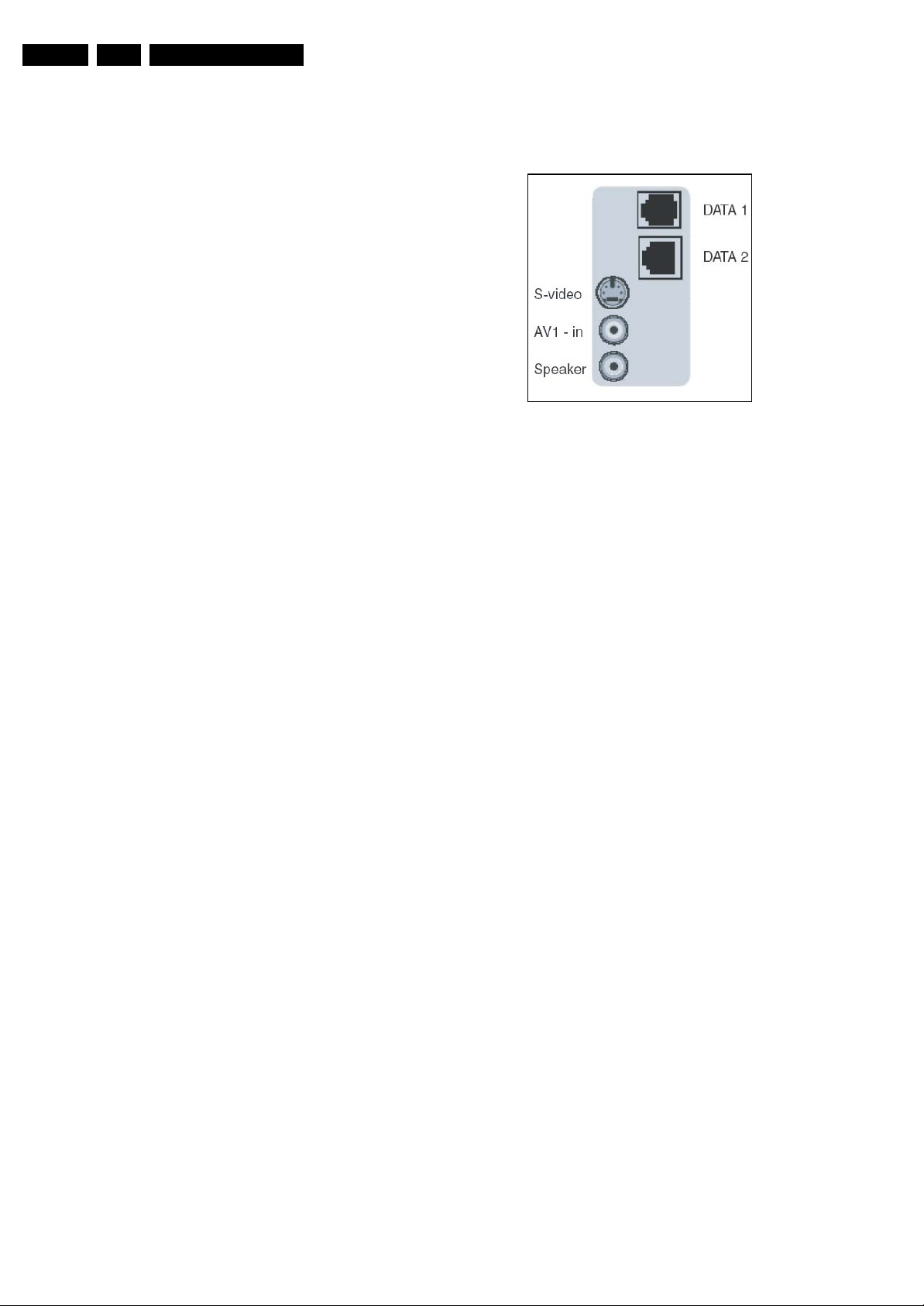
1.2.1 Side I/O connections
G_16250_040.eps
010806
Figure 1-1 Side I/O connections
RJ12 DATA1 (HM-Link - In/Out)
1 -LED_in < 0.3 V, active low j
2 -IR_in < 0.3 V, active low j
3-MODE Vcc j
4 -TV Power Status 4.5 to 5 V: TV “On”
< 0.3 V: TV “Stdby”
High impedance: TV “Off” k
5 - Gnd Gnd H
6 - IR_out Signal k
Response time (ms) : 8
Viewing angle (HxV degrees) : 176x176
1.1.2 Sound
Sound systems : Virtual dolby surround
: Dynamic Bass
Enhancement
Maximum power (W
) : 2 x 15
RMS
1.1.3 Miscellaneous
Power supply:
Mains voltage (V
) : 110 - 240
AC
Mains frequency (Hz) : 50 / 60
Ambient conditions:
- Temperature range (°C) : +5 to +40
- Maximum humidity : 90% R.H.
Power consumption:
Normal operation (W) : 65
Stand-by (W) : < 1
RJ45 DATA2 (Xpress Box - In/Out)
1 - +12V +12V/1W k
2 - Gnd Gnd H
3 - H-sync Signal k
4 - V-sync Signal k
5 - TXD232 Signal
6 - RXD232 Signal
7 - SDA3_IR-OUT Signal k
8 - DCM-POR Signal k
9 - CVBSterr Signal k
10 - Gnd CVBSterr Gnd H
S-Video (Hosiden): Video Y/C - In
1 - Ground Y Gnd H
2 - Ground C Gnd H
3 - Video Y 1 V
4 - Video C 0.3 V
/ 75 ohm j
PP
/ 75 ohm j
PP
AV1 Mini Jack: Video 1fH CVBS - In, Audio - In
1 - Audio R 0.5 V
/ 10 kohm oj
RMS
2 - Ground CVBS Gnd oj
3 - Video CVBS 1 V
4 - Audio L 0.5 V
/ 75 ohm oj
PP
/ 10 kohm oj
RMS
Mini Jack: Speaker - Out
- Loudspeaker 8 ohm ok
Dimensions
(WxHxD cm without stand) : 93.5 x 51.6 x 12.0
Weight (kg) : 19.2
1.2 Connection Overview
Note: The following connector color abbreviations are used
(acc. to DIN/IEC 757): Bk= Black, Bu= Blue, Gn= Green, Gy=
Grey, Rd= Red, Wh= White, and Ye= Yellow.
Page 3
Technical Specifications, Connections, and Chassis Overview
EN 3LC4.31HU AB 1.
1.2.2 Rear Connections
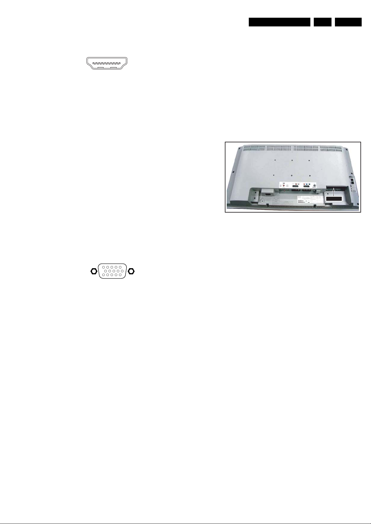
HDMI: Digital Video/Digital Audio - In
19
18 2
1
E_06532_017.eps
250505
Figure 1-2 HDMI (type A) connector
1 - D2+ Data channel j
2 - Shield Gnd H
3 - D2- Data channel j
4 - D1+ Data channel j
5 - Shield Gnd H
6 - D1- Data channel j
7 - D0+ Data channel j
8 - Shield Gnd H
9 - D0- Data channel j
10 - CLK+ Data channel j
11 - Shield Gnd H
12 - CLK- Data channel j
13 - n.c.
14 - n.c.
15 - DDC_SCL DDC clock j
16 - DDC_SDA DDC data jk
17 - Ground Gnd H
18 - +5V j
19 - HPD Hot Plug Detect j
20 - Ground Gnd H
Cinch: DVI Audio - In
Rd - Audio - R 0.5 V
Wh - Audio - L 0.5 V
/ 10 kohm jq
RMS
/ 10 kohm jq
RMS
VGA: Video RGB - In
1
5
6
11
10
15
E_06532_002.eps
050404
Cinch: Audio - In
Wh - Audio L 0.5 V
Rd - Audio R 0.5 V
/ 10 kohm jq
RMS
/ 10 kohm jq
RMS
Service connector (UART)
1 - UART_TX Transmit k
2 - Ground Gnd H
3 - UART_RX Receive j
Service connector (ComPair)
1 - SDA-S I
2 - SCL-S I
2
C Data (0 - 5 V) jk
2
C Clock (0 - 5 V) j
3 - Ground Gnd H
1.2.3 DCM Slot
Figure 1-4 DCM slot
The DCM slot can be used to connect consumer dedicated
applications on an Institutional TV set.
SDMDCM
G_16250_001.eps
270706
Figure 1-3 VGA Connector
1 - Video Red 0.7 V
2 - Video Green 0.7 V
3 - Video Blue 0.7 V
4-n.c.
/ 75 ohm j
PP
/ 75 ohm j
PP
/ 75 ohm j
PP
5 - Ground Gnd H
6 - Ground Red Gnd H
7 - Ground Green Gnd H
8 - Ground Blue Gnd H
9-+5V
10 - Ground Sync Gnd H
+5 V j
DC
11 - n.c.
12 - DDC_SDA DDC data j
13 - H-sync 0 - 5 V j
14 - V-sync 0 - 5 V j
15 - DDC_SCL DDC clock j
Cinch: Audio - In
Wh - Audio L 0.5 V
Rd - Audio R 0.5 V
/ 10 kohm jq
RMS
/ 10 kohm jq
RMS
Cinch: Video CVBS - In, Audio - In
Wh - Audio L 0.5 V
Rd - Audio R 0.5 V
Ye -Video CVBS 1 V
/ 10 kohm jq
RMS
/ 10 kohm jq
RMS
/ 75 ohm jq
PP
Cinch: Video YPbPr - In
Gn - Video Y 1 V
Bu -Video Pb 0.7 V
Rd - Video Pr 0.7 V
/ 75 ohm jq
PP
/ 75 ohm jq
PP
/ 75 ohm jq
PP
Page 4
EN 4 LC4.31HU AB1.
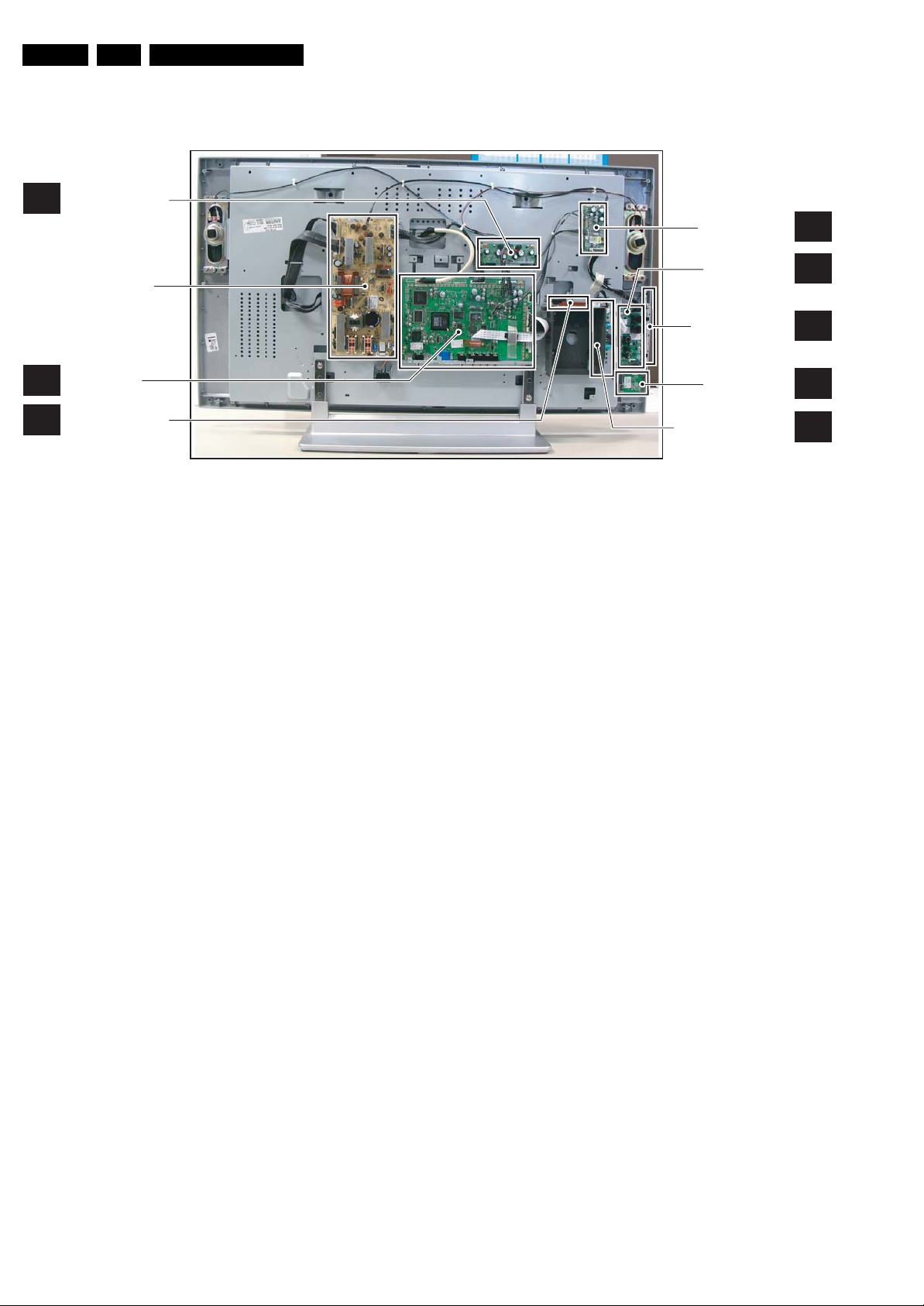
1.3 Chassis Overview
AUDIO AMPLIFIER
C
PANEL
Technical Specifications, Connections, and Chassis Overview
i-BOARD PANEL
HC
LCD SUPPLY
PANEL (item 1188)
SMALL SIGNAL
B
BOARD
SYSTEM INTERFACE
SI
PANEL
Figure 1-5 PWB/CBA locations (32” model)
G_16570_010.eps
180906
SIDE I/O PANEL
CONTROL PANEL
IR / LED PANEL
DC/DC
CONVERTER PANEL
D
E
J
DC
Page 5

Safety Instructions, Warnings, and Notes
2. Safety Instructions, Warnings, and Notes
EN 5LC4.31HU AB 2.
Index of this chapter:
2.1 Safety Instructions
2.2 Warnings
2.3 Notes
2.1 Safety Instructions
Safety regulations require the following during a repair:
• Connect the set to the Mains/AC Power via an isolation
transformer (> 800 VA).
• Replace safety components, indicated by the symbol h,
only by components identical to the original ones. Any
other component substitution (other than original type) may
increase risk of fire or electrical shock hazard.
Safety regulations require that after a repair, the set must be
returned in its original condition. Pay in particular attention to
the following points:
• Route the wire trees correctly and fix them with the
mounted cable clamps.
• Check the insulation of the Mains/AC Power lead for
external damage.
• Check the strain relief of the Mains/AC Power cord for
proper function.
• Check the electrical DC resistance between the Mains/AC
Power plug and the secondary side (only for sets that have
a Mains/AC Power isolated power supply):
1. Unplug the Mains/AC Power cord and connect a wire
between the two pins of the Mains/AC Power plug.
2. Set the Mains/AC Power switch to the "on" position
(keep the Mains/AC Power cord unplugged!).
3. Measure the resistance value between the pins of the
Mains/AC Power plug and the metal shielding of the
tuner or the aerial connection on the set. The reading
should be between 4.5 Mohm and 12 Mohm.
4. Switch "off" the set, and remove the wire between the
two pins of the Mains/AC Power plug.
• Check the cabinet for defects, to prevent touching of any
inner parts by the customer.
Service Default Mode (see chapter 5) with a colour bar
signal and stereo sound (L: 3 kHz, R: 1 kHz unless stated
otherwise) and picture carrier at 475.25 MHz for PAL, or
61.25 MHz for NTSC (channel 3).
• Where necessary, measure the waveforms and voltages
with (D) and without (E) aerial signal. Measure the
voltages in the power supply section both in normal
operation (G) and in stand-by (F). These values are
indicated by means of the appropriate symbols.
• Manufactured under license from Dolby Laboratories.
“Dolby”, “Pro Logic” and the “double-D symbol”, are
trademarks of Dolby Laboratories.
2.3.2 Schematic Notes
• All resistor values are in ohms, and the value multiplier is
often used to indicate the decimal point location (e.g. 2K2
indicates 2.2 kohm).
• Resistor values with no multiplier may be indicated with
either an "E" or an "R" (e.g. 220E or 220R indicates 220
ohm).
• All capacitor values are given in micro-farads (μ= x10
nano-farads (n= x10
• Capacitor values may also use the value multiplier as the
decimal point indication (e.g. 2p2 indicates 2.2 pF).
• An "asterisk" (*) indicates component usage varies. Refer
to the diversity tables for the correct values.
• The correct component values are listed in the Spare Parts
List. Therefore, always check this list when there is any
doubt.
2.3.3 BGA (Ball Grid Array) ICs
Introduction
For more information on how to handle BGA devices, visit this
URL: www.atyourservice.ce.philips.com (needs subscription,
not available for all regions). After login, select “Magazine”,
then go to “Repair downloads”. Here you will find Information
on how to deal with BGA-ICs.
-9
), or pico-farads (p= x10
-12
-6
),
).
2.2 Warnings
• All ICs and many other semiconductors are susceptible to
electrostatic discharges (ESD w). Careless handling
during repair can reduce life drastically. Make sure that,
during repair, you are connected with the same potential as
the mass of the set by a wristband with resistance. Keep
components and tools also at this same potential. Available
ESD protection equipment:
– Complete kit ESD3 (small tablemat, wristband,
connection box, extension cable and earth cable) 4822
310 10671.
– Wristband tester 4822 344 13999.
• Be careful during measurements in the high voltage
section.
• Never replace modules or other components while the unit
is switched "on".
• When you align the set, use plastic rather than metal tools.
This will prevent any short circuits and the danger of a
circuit becoming unstable.
2.3 Notes
2.3.1 General
• Measure the voltages and waveforms with regard to the
chassis (= tuner) ground (H), or hot ground (I), depending
on the tested area of circuitry. The voltages and waveforms
shown in the diagrams are indicative. Measure them in the
BGA Temperature Profiles
For BGA-ICs, you must use the correct temperature-profile,
which is coupled to the 12NC. For an overview of these profiles,
visit the website www.atyourservice.ce.philips.com (needs
subscription, but is not available for all regions)
You will find this and more technical information within the
"Magazine", chapter "Repair downloads".
For additional questions please contact your local repair help
desk.
2.3.4 Lead-free Soldering
Due to lead-free technology some rules have to be respected
by the workshop during a repair:
• Use only lead-free soldering tin Philips SAC305 with order
code 0622 149 00106. If lead-free solder paste is required,
please contact the manufacturer of your soldering
equipment. In general, use of solder paste within
workshops should be avoided because paste is not easy to
store and to handle.
• Use only adequate solder tools applicable for lead-free
soldering tin. The solder tool must be able:
– To reach a solder-tip temperature of at least 400°C.
– To stabilize the adjusted temperature at the solder-tip.
– To exchange solder-tips for different applications.
• Adjust your solder tool so that a temperature of around
360°C - 380°C is reached and stabilized at the solder joint.
Heating time of the solder-joint should not exceed ~ 4 sec.
Avoid temperatures above 400°C, otherwise wear-out of
tips will increase drastically and flux-fluid will be destroyed.
Page 6
EN 6 LC4.31HU AB2.
Safety Instructions, Warnings, and Notes
To avoid wear-out of tips, switch “off” unused equipment or
reduce heat.
• Mix of lead-free soldering tin/parts with leaded soldering
tin/parts is possible but PHILIPS recommends strongly to
avoid mixed regimes. If this cannot be avoided, carefully
clear the solder-joint from old tin and re-solder with new tin.
2.3.5 Alternative BOM identification
The third digit in the serial number (example:
AG2B0335000001) indicates the number of the alternative
B.O.M. (Bill Of Materials) that has been used for producing the
specific TV set. In general, it is possible that the same TV
model on the market is produced with e.g. two different types
of displays, coming from two different suppliers. This will then
result in sets which have the same CTN (Commercial Type
Number; e.g. 28PW9515/12) but which have a different B.O.M.
number.
By looking at the third digit of the serial number, one can
identify which B.O.M. is used for the TV set he is working with.
If the third digit of the serial number contains the number “1”
(example: AG1B033500001), then the TV set has been
manufactured according to B.O.M. number 1. If the third digit is
a “2” (example: AG2B0335000001), then the set has been
produced according to B.O.M. no. 2. This is important for
ordering the correct spare parts!
For the third digit, the numbers 1...9 and the characters A...Z
can be used, so in total: 9 plus 26= 35 different B.O.M.s can be
indicated by the third digit of the serial number.
2.3.7 Board Level Repair (BLR) or Component Level Repair (CLR)
If a board is defective, consult your repair procedure to decide
if the board has to be exchanged or if it should be repaired on
component level.
If your repair procedure says the board should be exchanged
completely, do not solder on the defective board. Otherwise, it
cannot be returned to the O.E.M. supplier for back charging!
2.3.8 Practical Service Precautions
• It makes sense to avoid exposure to electrical shock.
While some sources are expected to have a possible
dangerous impact, others of quite high potential are of
limited current and are sometimes held in less regard.
• Always respect voltages. While some may not be
dangerous in themselves, they can cause unexpected
reactions that are best avoided. Before reaching into a
powered TV set, it is best to test the high voltage insulation.
It is easy to do, and is a good service precaution.
Identification: The bottom line of a type plate gives a 14-digit
serial number. Digits 1 and 2 refer to the production center (e.g.
AG is Bruges), digit 3 refers to the B.O.M. code, digit 4 refers
to the Service version change code, digits 5 and 6 refer to the
production year, and digits 7 and 8 refer to production week (in
example below it is 2006 week 17). The 6 last digits contain the
serial number.
MODEL :
PROD.NO:
32PF9968/10
AG 1A0617 000001
220-240V 50/60Hz
VHF+S+H+UHF
S
Figure 2-1 Serial number (example)
2.3.6 Exchanging a Defective PDP
If a PDP has defective or "dead" pixels, do the following:
1. Locate the defective pixels.
2. Indicate their positions by means of a marker (with
erasable ink!).
3. Indicate the positions of the defective pixels in the Defects
Description Form (DDF), which is published in the PDP
manuals.
4. After this, remove the PDP and return it to your Service
organisation.
MADE IN BELGIUM
~
128W
BJ3.0E LA
E_06532_024.eps
130606
If a PDP has to be removed from the TV set, always keep in
mind that the PDP parts can easily be damaged by ESD, so
take the following protective measures:
• Do not damage the flex foils (they are located on the left,
right, upper and lower sides of the PDP).
• Do not scratch the glass plate.
• Avoid fingerprints.
Page 7

3. Directions for Use
You can download this information from the following websites:
http://www.philips.com/support
http://www.p4c.philips.com
Directions for Use
EN 7LC4.31HU AB 3.
Page 8
EN 8 LC4.31HU AB4.
Mechanical Instructions
4. Mechanical Instructions
Index of this chapter:
4.1 Cable Dressing
4.2 Service Position
4.3 Assy/Panel and STB removal (“piggy-backed” & “Smart
Card” STB versions)
4.4 Set Re-assembly
4.1 Cable Dressing
Notes:
• Only information that is related to the iTV module, is
published in this manual. For the other information, see
the relevant chassis manual (order code on front page).
• Some models in this chassis range have a different
mechanical construction. The information given here is
therefore model specific.
• Figures can deviate due to the different set executions.
4.2 Service Position
First, put the TV set in its service position. Therefore, place it
upside down on a table top (use a protection sheet or foam
bars).
4.2.1 The Foam Bars
The foam bars (order code 3122 785 90580) can be used for
all types and sizes of Flat TVs. By laying the plasma or LCD TV
flat on the (ESD protective) foam bars, a stable situation is
created to perform measurements and alignments. By first
placing a mirror flat on the table under the TV you can easily
see if something is happening on the screen.
Figure 4-1 Cable dressing (32” models)
Required for sets
1
42”
Figure 4-2 Foam bars
G_16570_011.eps
140906
1
E_06532_018.eps
171106
Page 9
Mechanical Instructions
s
6
s
6
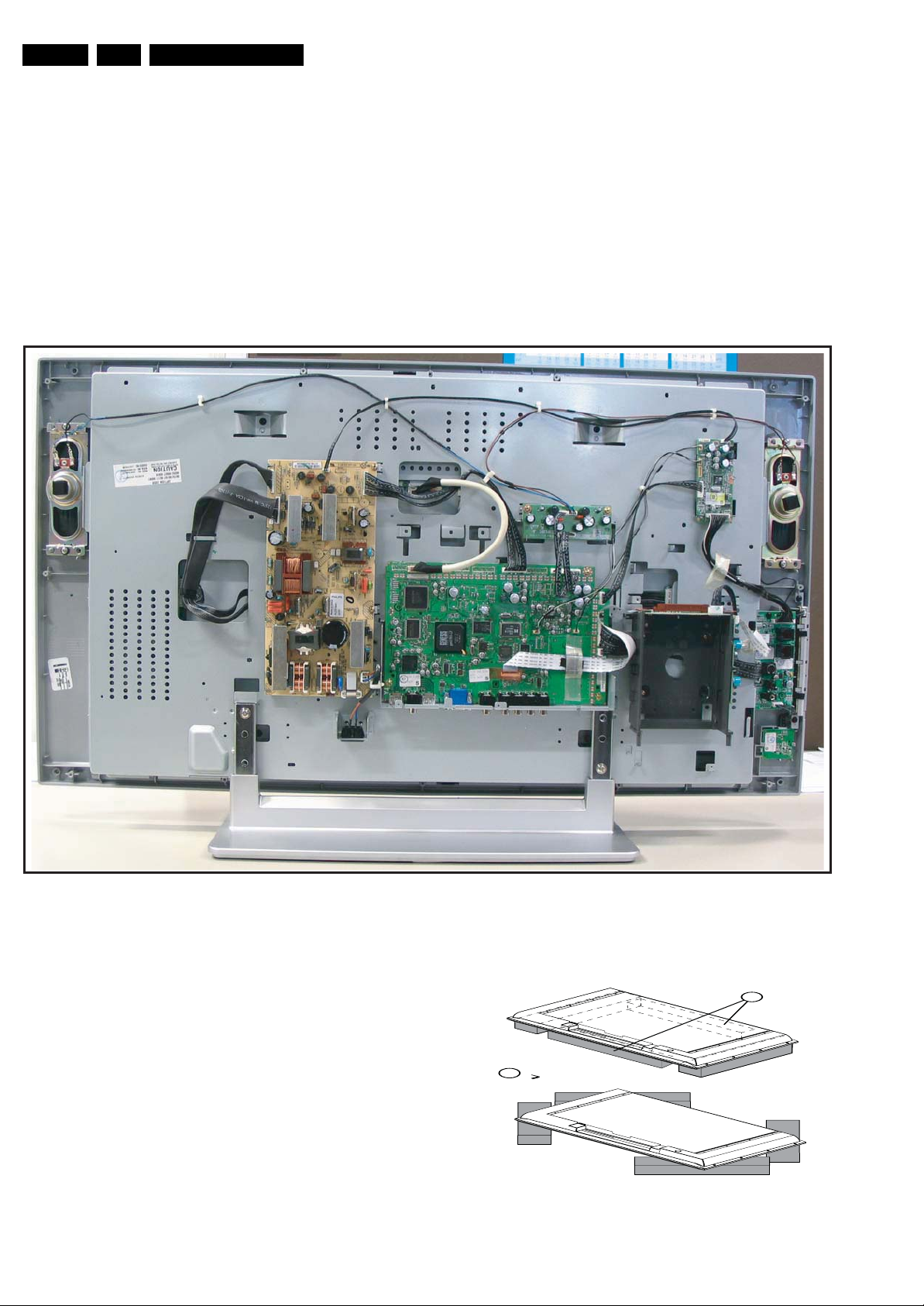
4.3 Assy/Panel and STB removal (“piggy-backed” & “Smart Card” STB versions)
4.3.1 Set Top Box and Bracket Removal (e.g. for TV-sets with STB “piggy-backed”on rear side)
EN 9LC4.31HU AB 4.
Warning: Before starting dismantling, disconnect all cables of
the Enseo Set Top Box and the TV set.
1. Remove the screws [1] of the Enseo cover.
2. Lift the Enseo cover from the bracket.
3. Do not damage cables and other internal components
while the Enseo cover is removed.
4. Disconnect all cables to and from the Enseo Set Top Box.
1
G_16570_006.eps
130906
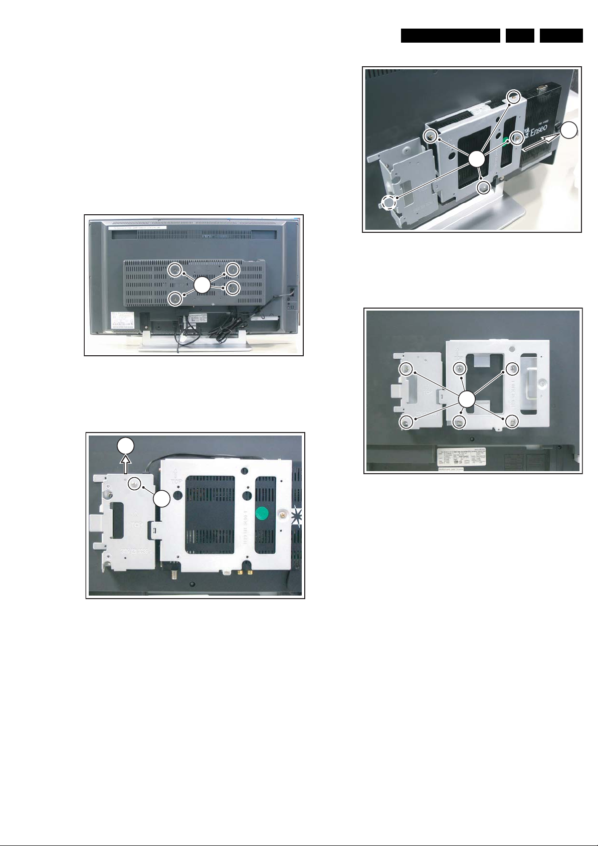
Figure 4-3 Set Top Box cover removal
5. Remove screw [1], and take the AC adapter from the
bracket [2] by sliding it upwards.
Figure 4-5 “Piggy-backed” STB removal
4.3.2 Rear Cover
2
1
G_16570_008.eps
140906
1
22
1
G_16570_007.ep
14090
Figure 4-4 12Vdc power adapter removal
6. Remove screws [1], and take the Enseo Set Top Box from
the bracket [2] by sliding it to the right.
Figure 4-6 STB bracket removal
1. Before the rear cover can be lifted from the TV set, all
external mounting brackets must be removed [1].
2. After the brackets have been removed, unscrew the rear
cover. Do not damage cables and other internal
components while the rear cover is lifted from the TV set.
4.3.3 i-Board Panel (32”)
Now you have access to the i-Board.
1. Remove all connectors from the i-Board.
2. Release the metal fixation clamp of the i-Board (e.g. bend
with a pair of pliers).
3. Remove the panel.
G_16570_009.ep
13090
Page 10
EN 10 LC4.31HU AB4.
4.3.4 DC/DC Converter Removal
Mechanical Instructions
3
1
2
G_16250_006.eps
Figure 4-7 DC/DC Converter removal (photo from 32HF7544D)
1. Remove connector [1] from the DC/DC Converter [2].
2. Carefully release the fixation clamps [3] and take out the
DC/DC Converter.
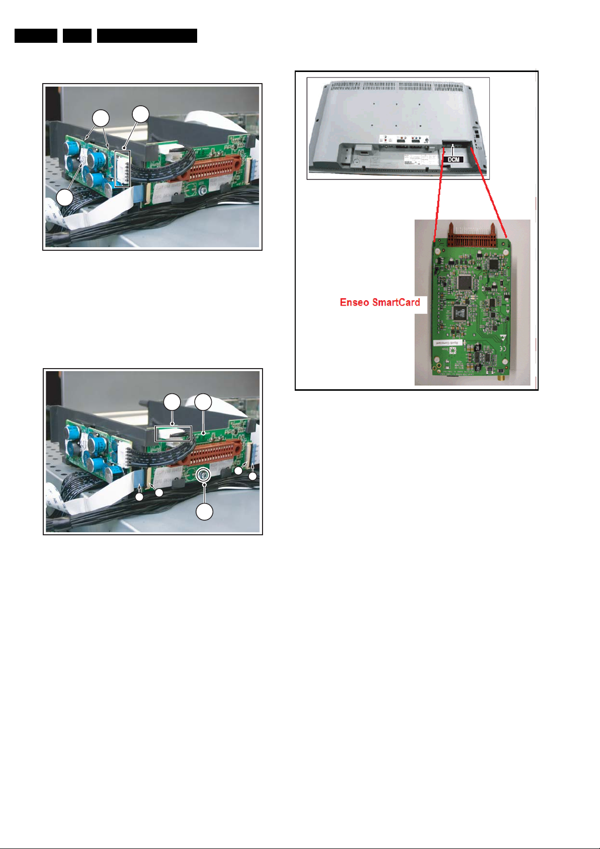
4.3.5 System Interface Removal
1 2
280706
G_16570_012.eps
130207
4
5
4
5
3
G_16250_002.eps
270706
Figure 4-8 System Interface removal
1. Remove connector [1] from the System Interface [2].
2. Remove screw [3].
3. Carefully lift the lever on both Flat Foil Connectors (FFC)
[4], on the left and right edge of the System Interface [2].
4. Pull out both Flat Foils [5].
5. Pull the System Interface out of the lower carriers.
6. To remove, place it in a backward position, and move down
the System Interface.
4.3.6 Enseo “Smart Card” Set Top Box Removal from DCM slot (only for TV-sets without “piggy-backed” STB on rear side)
Warning: Before removal of the “Smart Card” STB, switch off
the TV-set.
Figure 4-9 “Smart Card” Set Top Box removal
4.4 Set Re-assembly
To re-assemble the whole set, execute all processes in reverse
order.
Notes:
• While re-assembling, make sure that all cables are placed
and connected in their original positions. See Figure “Cable
dressing”.
Be careful with the fragile LVDS cable.
1. Remove the STB from the TV-set, by gently pulling it out of
its DCM slot (see picture “ ‘Smart Card’ Set Top Box
removal”).
Page 11
Service Modes, Error Codes, and Fault Finding
5. Service Modes, Error Codes, and Fault Finding
EN 11LC4.31HU AB 5.
Index of this chapter:
5.1 Hotel Mode, Service Modes
5.2 Error Codes
Notes:
• Only information that is related to the iTV module, is
published in this manual. For the other information, see
the relevant chassis manual (order code on front page).
5.1 Hotel Mode, Service Modes
5.1.1 Hotel Mode
Before the service modes can be activated, the set needs to be
switched into normal consumer mode (MTV-Mode) first. Use
an iTV setup remote control (type: RC2753/01, 12nc: 3139 228
88782) in “setup” mode, and key in the code “024995” directly
followed by the MENU button. The text messages “TV Is Now
In MTV Mode” and “Please Do A Cold Start!” appears on the
screen. Disconnect the set for a few seconds from the mains
supply, reconnect the set to the mains supply again. The set is
now in the normal consumer mode (MTV-Mode).
After repair, place the set into hotel mode (iTV-Mode) again.
Key-in the same code on the remote control as described
above. The text message “TV Is Now In ITV Mode” appears.
A cold start must be performed as described above. The set is
now in the hotel mode (iTV-Mode) again.
5.1.2 Service Modes
Only when the set is in normal consumer mode (MTV Mode),
all service modes can be accessed. Refer to the main chassis
manual for further explanation of the service modes.
5.2 Error Codes
The error code buffer contains all errors detected since the last
time the buffer was erased. The buffer is written from left to
right. When an error occurs that is not yet in the error code
buffer, it is displayed at the left side and all other errors shift one
position to the right.
Table 5-1 Error code overview
Error Error Description Check Item Diagram
0 No Error
1 Mis-match of TV (Hercules)
SW and Scaler SW
Software
versions
N.A.
2 +12V from PSU error PSU A
3Plasma I
2
C error (only for
N.A. N.A.
plasma sets)
2
C error while
4I
7801 B7 + B8
communicating with the
Genesis Scaler
5 +5V protection 7752 B6
6 General I
communication between
ADC, analogue tuner, and/or
Columbus I
2
7I
2
C error;
2
C failed
C error while
1102, 7L01,
7M00
B1 + B18
+ B19
7L01 B18
communicating with ADC
2
C error while
8I
7C01 B11
communicating with the
Scaler EEPROM
2
9I
C error while
7207 B2
communicating with the
Hercules EEPROM (NVM for
TV).
Remark: when the Hercules
EEPROM is defective, the
Hercules should operate with
its default values.
2
10 I
C error while
N.A. N.A.
communicating with the PLL
tuner
2
11 I
C error while
7M00 B19
communicating with the 3D
combfilter IC-7M00
(Columbus)
12 I
2
C error while
N.A. HC
communicating with i-Board
uP (only iTV sets)
2
13 I
C error while
N.A. N.A.
communicating with the
HDMI decoder IC-7D03 (only
for NAFTA and AP)
14 Read-write error with the
7B01 B10
Scaler SDRAM
2
15 I
C error while
N.A. N.A.
communicating with the OTC
2
C error while
16 I
communicating with EPLD or
7N00 B20 +
B21
Pacific III
2
17 I
C error while
N.A. N.A.
communicating with the
Digital Module (only for digital
sets)
18 IBO hardware error (only for
N.A. N.A.
digital sets)
Page 12

EN 12 LC4.31HU AB5.
5.3 Fault Finding and Repair Tips
5.3.1 General
Circuit diagram HC (chapter 7) shows the schematic diagram
of the i-Board together with IO for LC4.xHx. The main
microprocessor is the P89C664, a 64K flash microprocessor
from Philips. In some sets on the market, the P89C668 (96K)
microprocessor is used. There are 3 HEF switches (U2, U3,
U4) which select the different interface control protocols to
work with the external service providers. U7 is a RS232 IC.
The iTV i-Board is constantly powered by 5V, even when the
TV set is in its Stand-by mode or switched “off” by using the
power button on the local keyboard. The constant power supply
enables the i-Board to communicate constantly with the headend server of the service provider. In this chassis, only 3V3 is
available and this is converted to 5V.
5.3.2 Checking the i-Board
1. Check the voltages across C1 (= 3V3) and C4 (= 5V), for
32” type, (resp. C75 and C81 for 37” type).
If these are correct, the 3V3 to 5V converter is working
properly.
2. Check the clock signal on pin 2 (SCL), and data line pin 3
(SDA) of the i-Board microprocessor P89C664 with an
oscilloscope. If the communication between the
microprocessor P89C664 and the TV scaler board is
working correctly, the iTV OSD menu will appear when the
menu button on the setup remote control is activated.
3. Check pin 4 of the microprocessor P89C664, it should be
low when the microprocessor is operating normally. Pin 4
goes to the “high” state and causes the microprocessor to
“hang” if the supply voltage drops below 4.5 - 4.75V. U6 is
used to reset the microprocessor and to monitor the supply
voltage.
4. Check (using an oscilloscope) if the sine wave (16 MHz) is
present on pin 14 and 15 of the microprocessor P98C664
(internal Xtal oscillator).
Service Modes, Error Codes, and Fault Finding
5.3.3 Checking the Enseo “Smart Card” STB
1. Check if the TV-set is able to display “coded/scrambled”
signals as well as uncoded ones. If the set does not display
coded signals, the STB may be defective. In this case, the
STB module has to be treated as a “black box” and to
replaced by a new one. The defective one must be send
back for repair.
Page 13
Block Diagrams, Test Point Overviews, and Waveforms
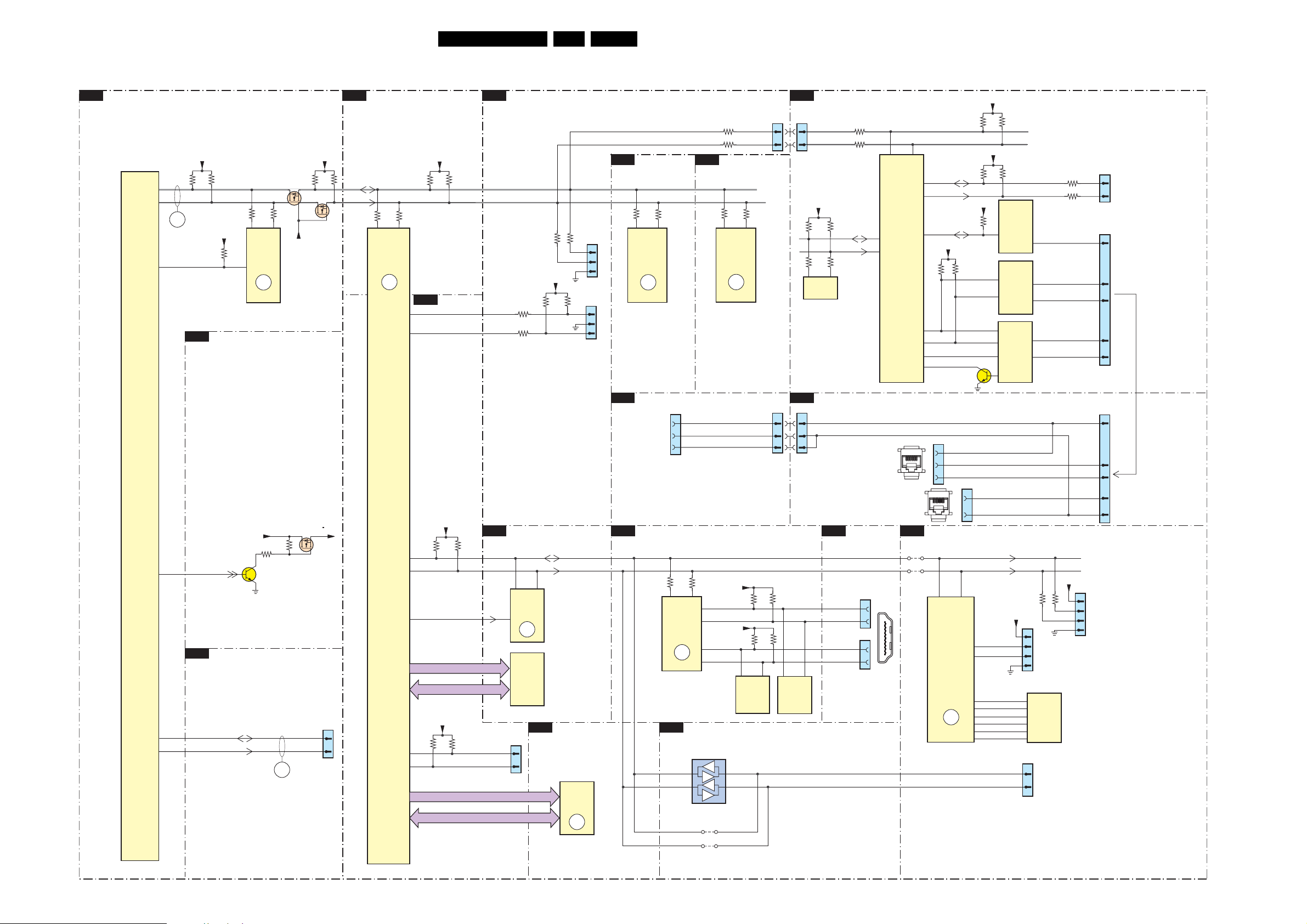
6. Block Diagrams, Test Point Overviews, and Waveforms
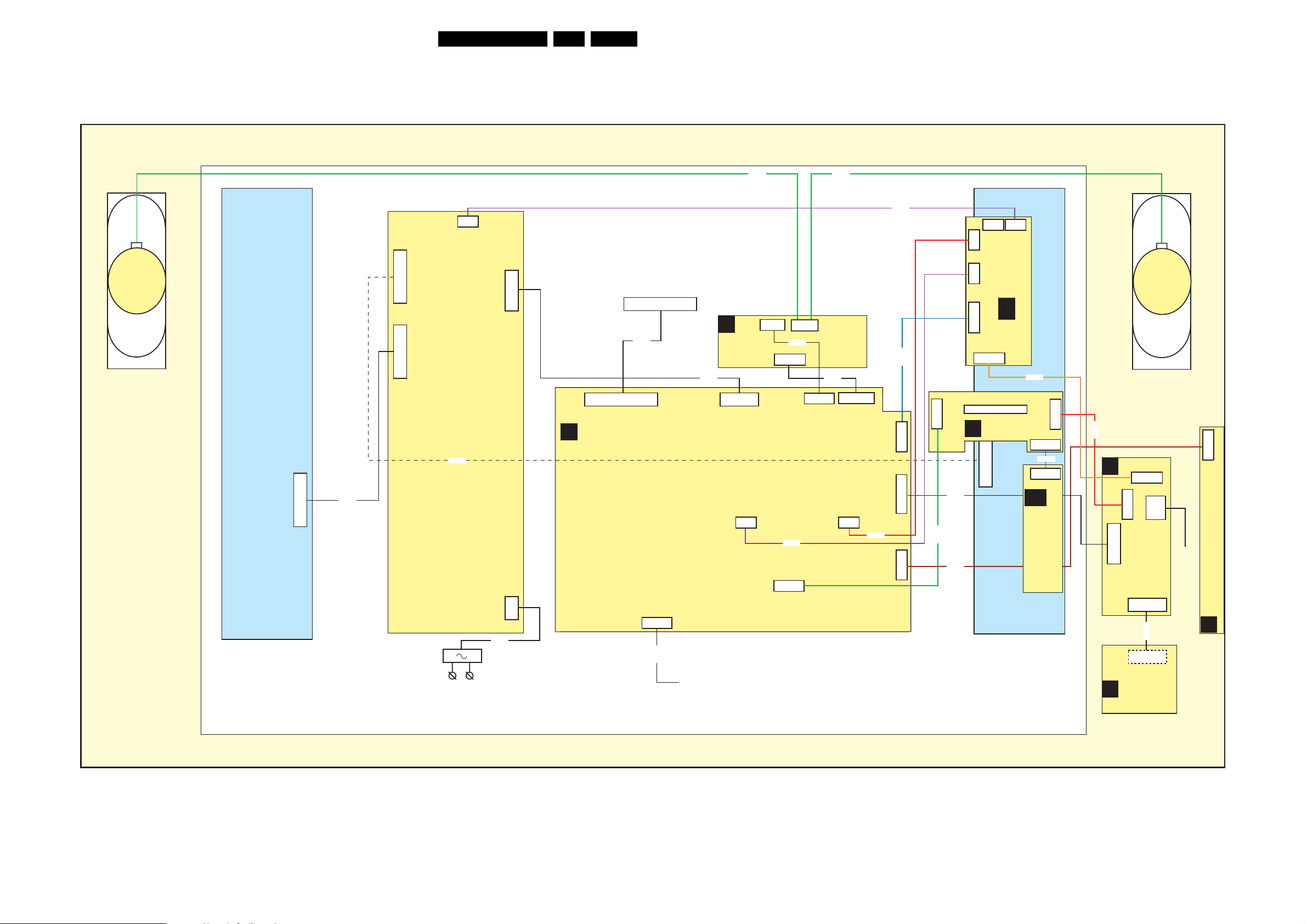
Wiring Diagram 32”
WIRING 32”
13LC4.31HU AB 6.
RIGHT
SPEAKER
14P
8520
X530
X520
12P
14P
3P
X220
POWER
SUPPLY
8520
AC POWER
INLET
POWER
IN
8002
X200
X002
12P
2P3
B
SSB
LVDS CONNECTION
TO DISPLAY
30P
8P06
30P
31P
1N16
HDMI
19P
8411
LCD PANEL
C
CLASS D
AUDIO
AMPLIFIER
8J02
TO ENSEO
SET TOP BOX
12P
1J02
1440
5P
8903
1003
3P
8J03
1002
9P
8402
1G03
32P
4P
1001
3P
1J03
8903
8J04
1J04(1M52)
1103
4P
9P
8403
8400
8407
6P
1K00(1M21)
12P
1K01(1M06)
3P
1K02
32P
8408
J1
8K01
8684
4P
5P
8P6
SI
INVERTERINVERTER
3P
4P
J10
J1
J2
J3
I-BOARD
HC
J6
J4
24P
J3
32P
SYSTEM
INTERFACE
12P
8406
DC
J4
J2
6P
8410
6P
J4
DC/DC
CONVERTER
20P
8409
D
J
LEFT
SPEAKER
SIDE AV
24P
1301
20P
RJ12
1309
1302
12P
1321
1340
5P
8870
5P
1540
IR/LED/LIGHT
SENSOR
TO ENSEO
SET TOP BOX
3P
KEYBOARD CONTROL
E
1684
G_16570_001.eps
130906
Page 14
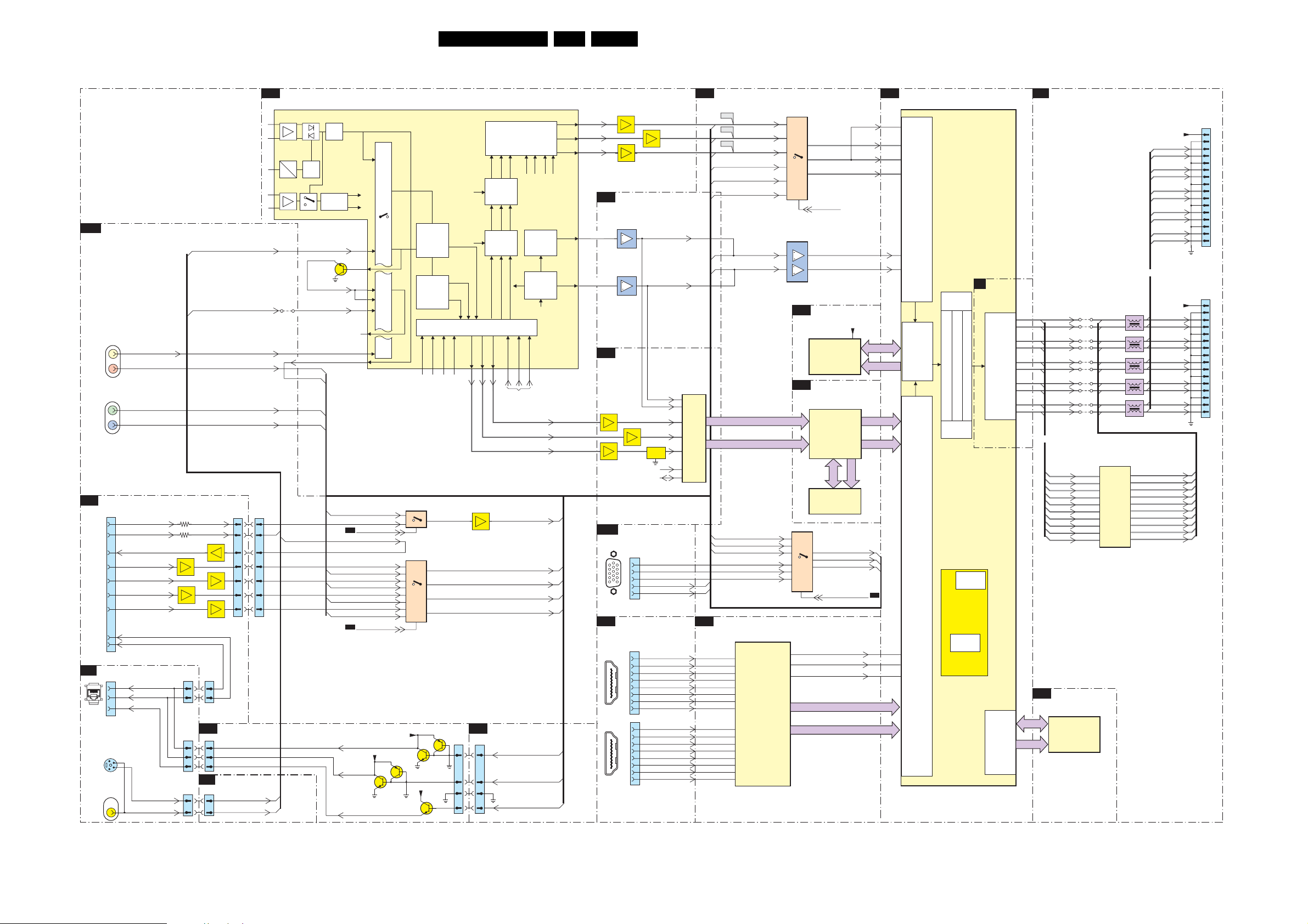
Block Diagrams, Test Point Overviews, and Waveforms
Block Diagram Video
VIDEO
(WITH SYSTEM INTERFACE FOR DATA COMMUNICATION MODULE)
CINCH ANALOGUE I/O
B23
1R07
1R06
J3
31
32
22
17
18
19
20
11
12
1303
1305
1
2
SVHS
1376
4
3
9
3
4
SC1_CVBS_IN
R55
YIN_32 CVBS_YIN
FBL_IN
R63
Q1,Q2,Q4
EF
Q5,Q11,Q12
EF
1309
17
16
1301
9
8
13
1321
4
2
CIN_32 C_IN
SC2_CVBS_OUT
B_PB_IN
G_Y_IN
R_PR_IN
HSYNC_OUT
VSYNC_OUT
VSYN
HSYN
CVBSterr
FRONT_C_IN
FRONT_Y_CVBS_IN
VIDEO
OUT
Pr
Y
Pb
SYSTEM INTERFACE
SI
32P CONN
FOR DCM
SIDE AV
D
RJ45
CONN.
5
S-VHS
VIDEO
IN
Q14
EF
Q3,Q9,Q10
EF
Q7
EF
J4
17
16
I-BOARD
HC
J4
9
8
13
SIDE
B17
CONNECTIONS
1K01
4
FRONT_YCVBS_IN
2
FRONT_C_IN
FRONT_Y_CVB
SC1_CVBS_IN
CVI_Pr_IN
CVI_Y_IN
CVI_Pb_IN
J1
8 8
22 22
20 20
10 10
12 12
14 14
15 15
FRONT_C_IN
S_IN
1G03
B2
7217
TDA15021H
24
25
31
29
30
B15a
HERCULES
AC
Detect
DC
4R64
SC1_CVBS_RF_OUT
7G11_12
B15a
B15a
Sound
Traps
AGC
QSS Mixer
AM Demod.
SC2_AV3_C_IN
CVBS_COMB
SC2_Y_IN_1
B3
CVBS1
Video
Switch
Control
QSS/FM
AM
59
7206
64
51
52
58
48
55
43
SC2_AV3_Y_IN
DMMI_CVBS_IN|Y_IN
AV2_DMMI_SW
B2
SC2_CVBS_MON_OUT
DMMI_B_Pb_IN
CVI_Pb_IN
DMMI_G_Y_IN
CVI_Y_IN
DMMI_R_Pr_IN
CVI_Pr_IN
FBL_HSYNC_PIN16_IN
SC1_FBL_IN
DMMI_RGB_SW
B2
HSYNC
+5VA
VSYNC
CVBSTERR
14LC4.31HU AB 6.
MUX-SYNC INTERFACE
B13
7208
7210
EF
7209
EF
EF
RGB Matrix
Blue & Black
Strech
Gamma Corr.
RO
85
RO
GO
86
GO
BO
87
BO
HERCULES
B_OSD
R_OSD
+
c
Dig. 2H/4H
Combfilter
Y Delay Adj.
Chroma
PAL / N TSC/
SECAM
Decoder &
Baseband
Delay
INSSW3
R/Pr-3
G/Y3
77 78 79 80
4
8
13
18
3
Q10
Q11
Q2
Yint
Uint
Vint
RGB/Pr Pb Insert
B/Pb-3
J3
cvbs/y
7R60
3
5
10
7R68
19
17
12
14
9
7
2
14
10
+5VA
Q8
Q9
+5VA
Skin Tone
SAT
U/V Tint
Saturation
SCAVEM
Peaking
on text
SCAVEM
U/V Delay
YUV Interface
YOUT
VOUT
UOUT
74 75 76 70 71 72
7R61
EF
SC1_CVI_DMMI_R_Pr_IN
SC1_CVI_DMM
SC1_CVI_DMM
SYNCINTERFACE
B3
1440
3
3
4
4
2
2
1
1
G_OSD
YUV
Vertical &
East-West
Geometry
YUV in/out
Sync Sep
H/V
H-OSC
H-Shift
H-Drive
CVBS/Y
VIN
UIN
YIN
N.C.
INTF_V_OUT
INTF_U_OUT
INTF_Y_OUT
SC2_Y_IN_1
I_G_Y_IN
I_B_Pb_IN
SC1_FBL_IN_
1
Hsync_SDTV
Vsync_SDTV
SC1_CVBS_RF_OUT
Fast Blanking
SYNC INTERFACE
B3
VSYNC
HOUT
B18
7L61/7L62
EF
7L71
EF
B23
5
1
PC-VGA/
CVI-2
B22
1
19
HDMI-1
1
19
HDMI-2
7436-2
7436-1
4 3
2 1
Vsync_SDTV
Hsync_SDTV
ADC
7L51/7L52
EF
7L72
VIN VOUT
COM
SCL
SDA
SCART ANALOG IO
1R02
10
1
15
2
3
6
13
11
14
DIGITAL IO
1F02
1
3
4
6
7
9
18 2
10
12
1F03
1
3
4
6
7
9
18 2
10
12
2
3
11
6
9
37
38
FBL_HSYNC_
PIN16_IN
VSYNC_IN
RX2+A
RX2-A
RX1+A
RX1-A
RX0+A
RX0-A
RXC+A
RXC-A
RX2+B
RX2-B
RX1+B
RX1-B
RX0+B
RX0-B
RXC+B
RXC-B
7L01
P3563M-LF
CONV.
VDRB
22
HOUT
67
B2
B2,B13
B2,B13
B2,B13
B2,B13
B3
B3
B2
A/D
B13
B13
B13
B3
B3
B15b
B15b
B15b
B12
FE00
R_OTC_SDTV
FE01
G_OTC_SDTV
FE02
B_OTC_SDTV
SC1_R_CVI_Pr_IN
SC1_G_CVI_Y_IN
SC1_B_CVI_Pb_IN
Vsync_SDTV
Hsync_SDTV
COL_Di(1-9)
COL_YA(1-9)
SC1_CV1_DMMI_R_Pr_IN
SC1_CV1_DMMI_G_Y_IN
SC1_CV1_DMMI_B_P
GINA|YINA
B13
B13
HDMI
7D03
TDA9974AEL
A9
A10
A12
A13
PANELLINK
A15
RECEIVER
A16
F16
G16
C10
C9
C13
C12
C16
C15
G14
F14
b_IN
RINA|Pr
BINA|Pb
HDMI
7E01
27
3
7
25
1
5
5
1
13
12
7E04
1
3
2
5
B10
B19
7E00
A2
A1
D1
R-PR-ADC
17
G-Y-ADC
14
B-PB-ADC
11
9
I_PC_HD_SEL
8
4
SDRAM
7B01
K4D263238I
1Mx32x4
COLUMBUS
(Dig. PAL/NTC Comb)
7M00
T6TU5XBG
COLUMBUS
DIGITAL COMB
7M01
MSM56V16
512Kx16x2
14
15
4
9
HDMI_CbCr(1-7)
SDRAM
FILTER
DRAM
SC1_R_CVI_Pr_IN
SC1_G_CVI_Y_IN
SC1_B_CVI_Pb_IN
RGB|CVI_HDA_SEL
HDMI_VCLK
HDMI_Y(0-7)
+2V5_DDR
COL_A
H_HDMI
V_HDMI
SOG
R_PR+
G_Y+
B_PB+
AVSYNC
AHSYNC
95
COL_Do(1-8)
COL_YB(1-8)
COL_DQ
FSDATA
FSADDR
B7
B13
B13
B13
B7
C3
D2
C2
B2
L3
L4
C14
B14
D16
SCALER
7801
GM1501
ANALOG
INPUT
PORT
FRAME
STORE
CONTROL
DVI/HDMI
INPUT
PORT
SCALER
GRAPHIC
ZOOM
OUT BLENDER
OSD CONTROLLER
BRIGHTNESS/CONTRAST/HUE/SAT
VIDEO
ZOOM
UART
INTERFACE
MICRO
CONTROLLER
INTERNAL
RAM
B9
SCALER
DISPLAY
TIMING
GEN.
EXTERNAL
ROM
INTERFACE
AE16
AF16
AE15
AF15
AE14
AF14
AF12
AF11
AF13
AE12
OCMADDR
B20
B11
OCMDATA
PACIFIC3
TXB0TXB0+
TXB1TXB1+
TXB2TXB2+
TXB3-
TXB3+
TXBCTXBC+
OR
TXB0+
TXB0TXB1+
TXB1TXB2+
TXB2TXB3+
TXB3-
TXBC+
TXBC-
FLASH/CONTROL
7C03
M29W400DT55N6E
FLASH
ROM
512Kx8
4N02
4N01
4N04
4N03
4N06
4N05
4N10
4N09
4N08
4N07
29
28
32
31
35
34
41
40
37
38
1N12
TXO0TXO0+
1N13
TXO1TXO1+
1N14
TXO2TXO2+
1N15
TXO3TXO3+
1N11
TXOCTXOC+
7N00
T6TF4AFG
LVD S
PACIFIC3
(RES For PIXEL+)
103
102
101
100
99
98
93
92
96
95
OR
LVD S_VCC
LVD SALVD SA+
LVD SBLVD SB+
LVD SCLVD SC+
LVD SDLVD SD+
LVD SCLKLVD SCLK+
LVD S_VCC
LVD SALVD SA+
LVD SBLVD SB+
LVD SCLVD SC+
LVD SDLVD SD+
LVD SCLKLVD SCLK+
TXO0-
TXO0+
TXO1-
TXO1+
TXO2-
TXO2+
TXO3-
TXO3+
TXOC-
TXOC+
1N16
1
11
12
13
14
15
16
17
18
19
20
24
25
26
21
22
1N17
1
11
10
12
14
13
15
19
18
20
27
26
28
22
21
23
G_16570_002.eps
121006
TO DISPLAY (26” & 32”) TO DISPLAY (LCD 37” & 42”, PDP 42” & 50”)
Page 15
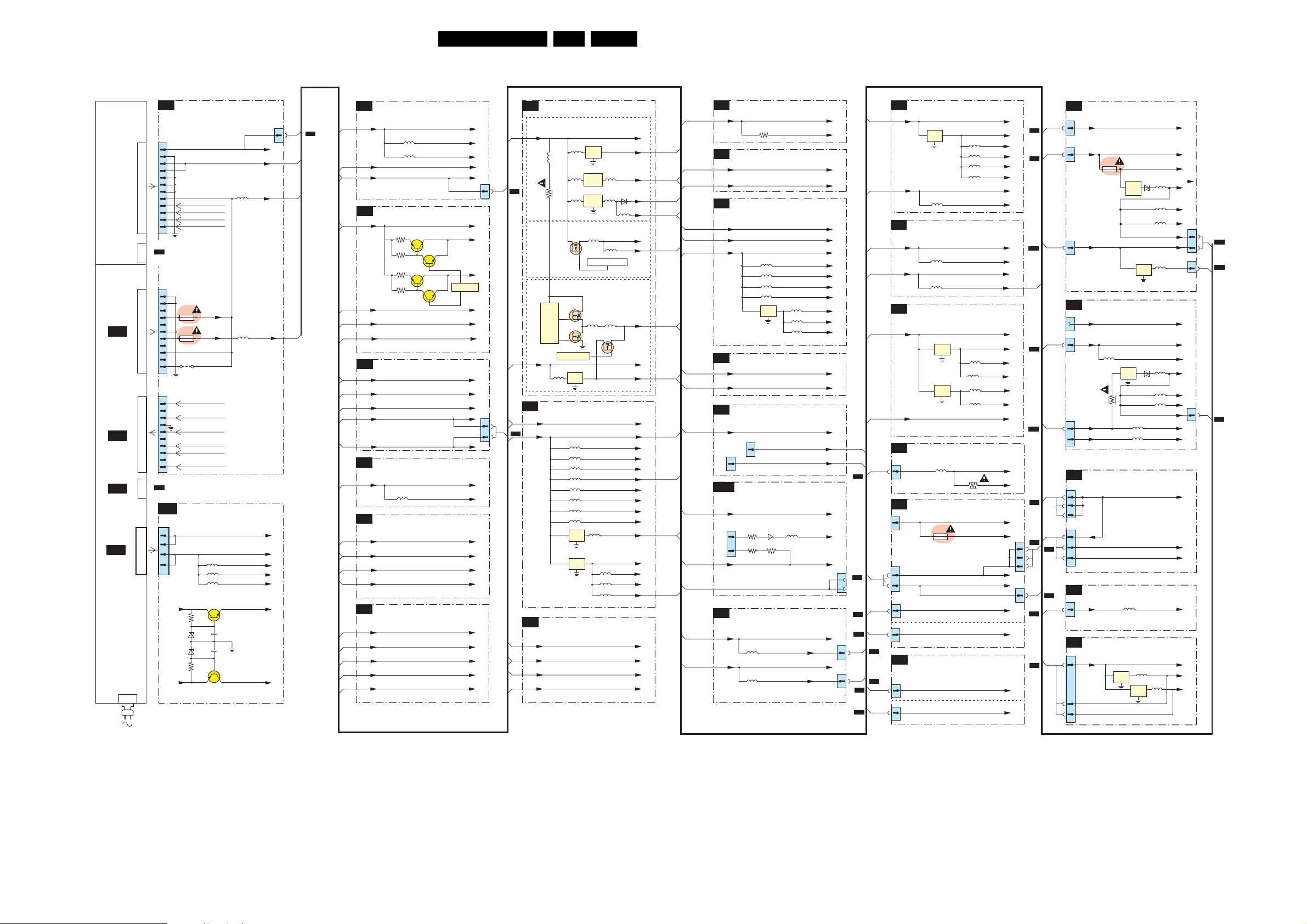
Block Diagrams, Test Point Overviews, and Waveforms
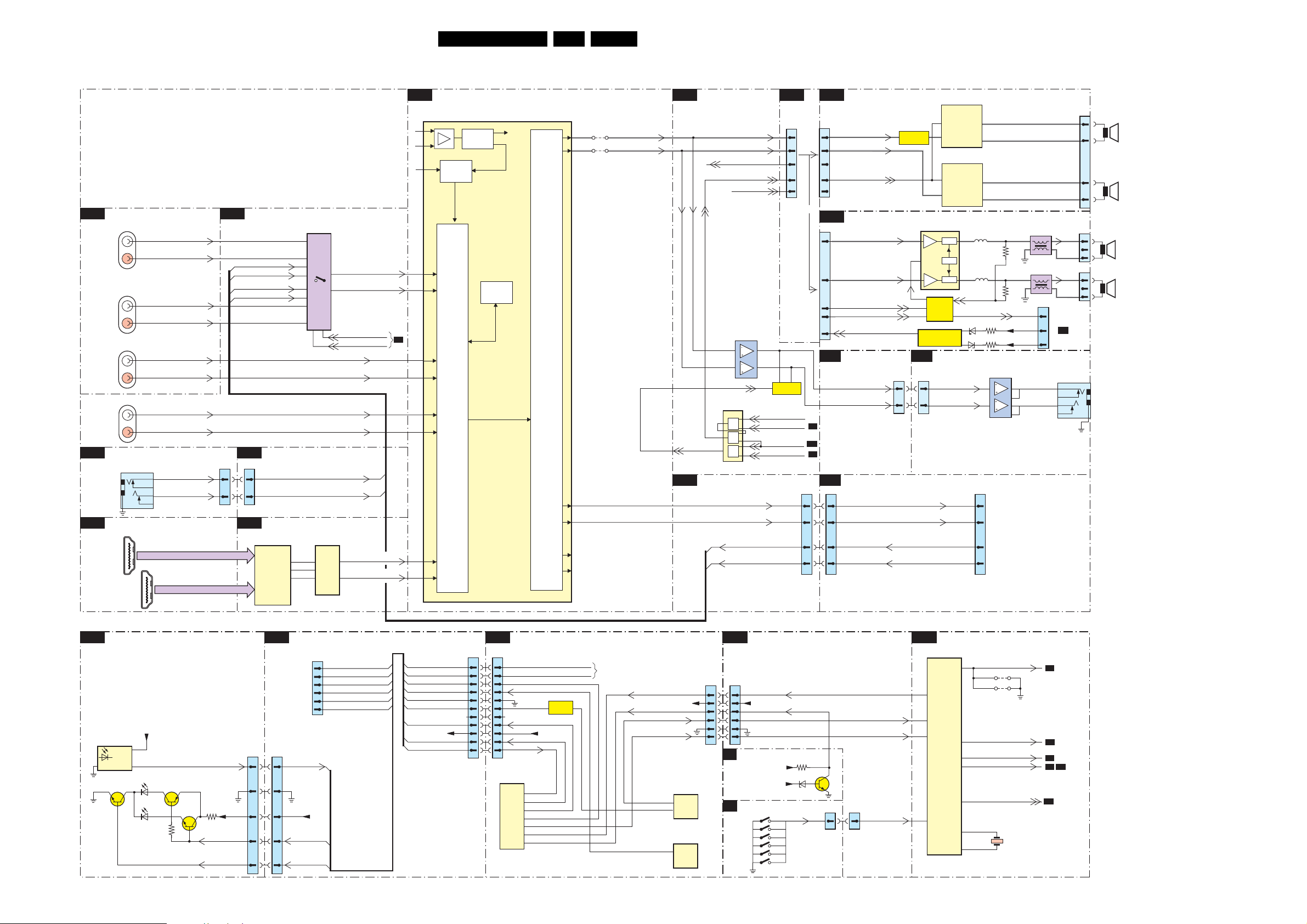
Block Diagram Audio & Control
AUDIO
CINCH ANALOGUE I/O
B23
1R07
AV
AUDI O
L/R IN
1R08
CVI-2
AUDI O
L/R IN
1R06
CVI-1
AUDI O
L/R IN
1F01
DVI
AUDI O
L/R IN
SIDE AV
D
1376
AUDI O
L/R IN
DIGITAL I/O
B22
1Q02
1
HDMI 1
19
HDMI 2
18 2
1Q03
1
19
AV1_Audio_INL
AV1_Audio_INR
AV2_Audio_INL
AV2_Audio_INR
HD_AudioINL
HD_AudioINR
DVI_D_AudioINL
DVI_D_AudioINR
L_FRONT_IN
7
R_FRONT_IN
1
2
HDMI_A
HDMI_B
18 2
B22
DMMI_AuidioINL
DMMI_AuidioINR
1330
66
88
DIGITAL I/O
SIDE_AudioINL
SIDE_AudioINR
SIDE CONNECTORS
B17
1K04
HDMI
B12
7D03
TDA9975
HDMI
10-BIT
VIDEO
CONVERTER
1
12
4
11
5
14
2
15
A5
A7
B7
7Q03
3
13
9
10
HD_AudioINL
HD_AudioINR
DVI_D_AudioINL
DVI_D_AudioINR
SIDE_AudioINL
SIDE_AudioINR
7D04
UDA1334ATS
DAC
1
3
2
Analog_AudioINL
Analog_AudioINR
Analog_AudioSEL1
Analog_AudioSEL2
HDMI_AudioINL
14
HDMI_AudioINR
16
15LC4.31HU AB 6.
HERCULES
B2
7217
TDA15021H
29
AD Conv.
Std Stereo
Decoder
AUDI O
SELECT
ADC/DAC
AM Demod.
30
33
34
35
B7
49
50
56
57
53
54
QSS Mixer
AM
QSS/FM
I2S
Processor
AUDI O
CONTROL
Vol/Treb/
Bass
Features
DACs
4211
61
60
36
37
62
63
4212
AUDOUTLSR
AUDOUTLSL
AUDIO PROCESSING
B5
SOUND-ENABLE
OUT_MUTE
3
6
OUT_MUTE
B23
8
CINCH ANALOGUE I/O
HER_SC2_AudioOutL
HER_SC2_AudioOutR
AUDI O-R
AUDIO-L
PROTECT_AUD
POR_AUDIO
7601
TS482ID
2
6
7602
74HC08PW
2
&
1
&
5
9
&
10
DMMI_AuidioINL
DMMI_AuidioINR
B16 C
1J04
1
7
7606
MUTE
HP_DET_R_DC_1
SOUND_ENABLE
POWER_DOWN
EXT_MUTE
AUDIO AMPLIFIER
(CLASS-D)
1002
33
11
77
88
99
FOR 32” ONLY
OR
SA3
1739
1
3
8
9
7
FOR 37”- 42” ONLY
B17
B2
B16
B2
1R03
44
66
18 18
16 16
(ONLY FOR SETS WITH SYSTEM INTERFACE GOR DATA COMMUNICATIE MODULE)
AUDI O-R
AUDI O-L
SOUND-ENABLE
AUDIO
AUDIO-L
AUDIO-R
SOUND-ENABLE
POR-CLASSD
PROT_AUDIOSUPPLY
SIDE
CONNECTORS
HP_LOUT
HP_ROUT
SYSTEM INTERFACE
SI
J1
7004
PHASE
INVERTER
1K01
(1K04)
10 10
11 11
AUD_R_OUT
AUD_L_OUT
RIGHT_AUDIO_IN
LEFT/MONO_AUDIO_IN
7700
TDA7490
10
stby-
6
mute
18
7701÷7707
SOUND
ENABLE
7708÷7711
AUDIO SUPPLY
PROT, CIRCUIT
D
1330
HEAD_PH_L
HEAD_PH_R
7001
TDA8931T
POWER
COMPARATOR
7
4
IN+
7000
TDA8931T
POWER
COMPARATOR
7
4
IN+
PWM
OSC
PWM
SIDE AV
OUT
HVPI
HVPI
3
23
PROT1
DCPROT
6703
6702
OUT
5702
5701
J3
16
13
16
13
3764
3761
7309
TDA1517ATW
3
18
AMPLIFIER
4
6
32P CONN
FOR DCM
18
16
3717
3718
-16 V-19V
+16 V+19V
8
9
12
13
5731
5730
1M02
7
1
5
TO 1M02
A
SUPPLY
1010
7
6
2
1001
1736
1735
4
3
SPEAKER
2
1
SPEAKER
1
2
3
SPEAKER
1
2
3
SPEAKER
BATHROOM
SPEAKER
RIGHT
LEFT
LEFT
RIGHT
CONTROL
IR LED PANEL
J
6541
GND
7542
OUT
SIDE AV
D
1302
LEDIN_CLK
1
IRIN_DATA-IN
2
3
RJ12 CONN
+5VA
VS
6540B
7540
Green
6540A
Red
3544
7541
3540
IR
+5VA
LED-SEL
PC-TV-LED
1540
44
55
22
33
11
1540
RC_IR
RD_GR_LED
LED_CTRL
MODE
4
STATUS_DATA-OUT
GND
5
6
IR_OUT
+5V
LEDIN_CLK
IRIN_DATA-IN
MODE
STATUS_DATA-OUT
GND
IR_OUT
LED_CTRL
RD_GR_LED
RC_IR
1301
+5V
11
22
33
44
55
66
17 17
20 20
21 21
22 22
23 23
I-BOARD
HC
J4
LEDIN_CLK_TXD_SCL1
IR_IN_DATA- IN_RXD_SDA1
MODE
STATUS_DATA_OUT
IR_OUT
PC_TV_LED_OUT
LED_SEL_OUT
RC_IR
U5
P89C664
MICRO
CONTR.
SIDE CONNECTORS
B17
See Blockdiagram
I²C
PC_TV_LED
CONTR.
+5V
9
18
13
11
1
10
40
+3V3STBY
LED-SEL
IR_IN_TV
LIGHT-SENSOR
15
4
4
U4
HEF4053BT
MULTI
PLEX
U3
HEF4053BT
MULTI
PLEX
1K00
J6
66
55
44
33
22
71
SYNC INTERFACE
B3
KEYBOARD CONTROL
E
Channel+
Channel-
Volume+
Vol ume -
Power
Menu
+3V3STBY
+3V3STBY
+5VSW
1703
1704
1701
1702
1706
1705
PC-TV-LED
LED-SEL
3431
6430
KB
7430
1684
LIGHT-SENSOR
1K02
22
IR
KEYBOARD
B2
7217
TDA15021H
107
97
115
120
HERCULES
HERCULES
127
10
11
114
102
111
122
SEL_IF_SDM
4204
4205
SERVICE
SMD
EXT_MUTE
SOUND-ENABLE
SC_STANDBY
AV2 _DMMI_SW
1202
B1
B5
B5
B6
B15
B15
G_16570_003.eps
130906
Page 16
Block Diagrams, Test Point Overviews, and Waveforms
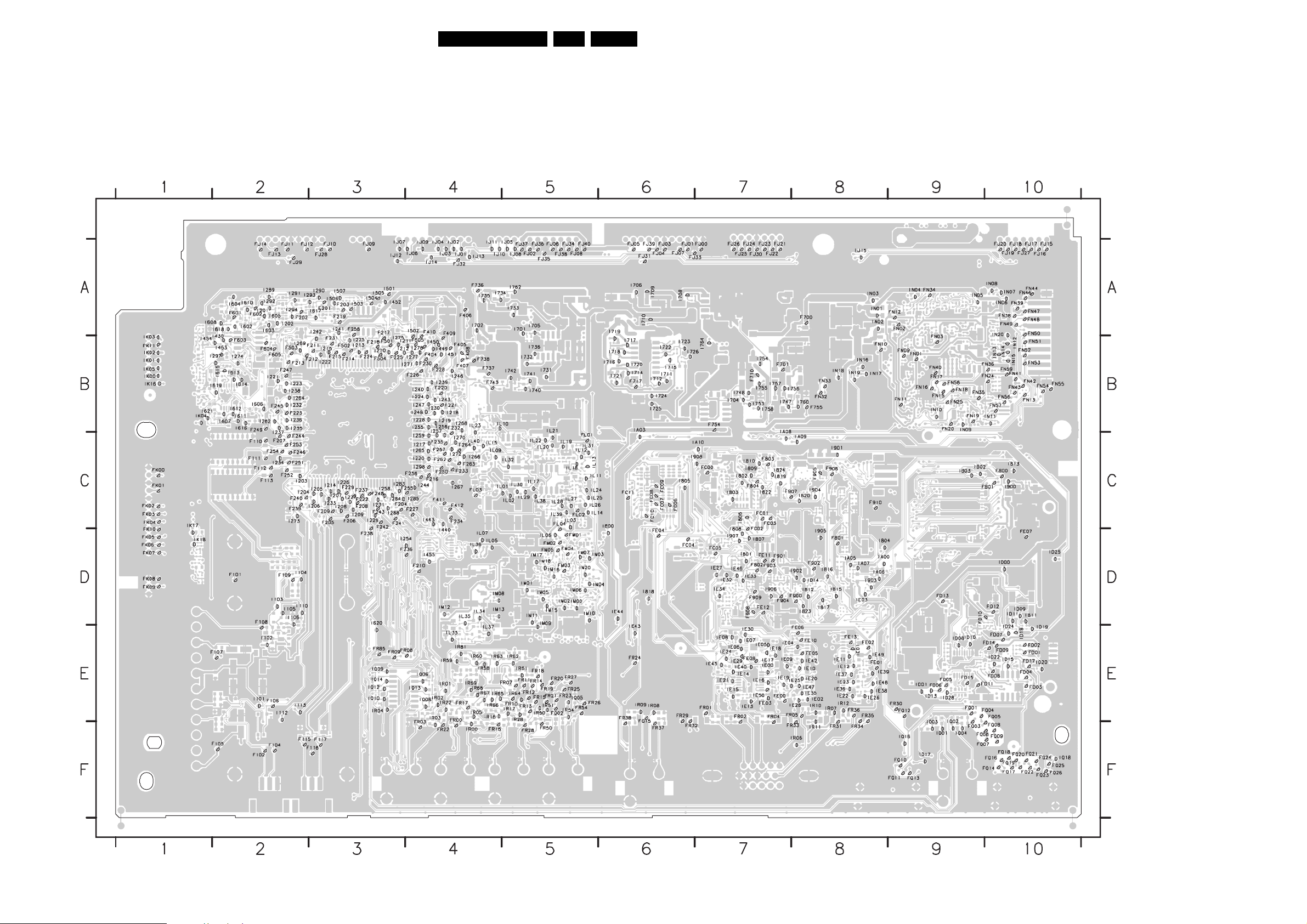
Test Point Overview SSB
F101 D2
F102 F2
F104 F2
F105 F2
F106 E2
F107 E2
F108 D2
F109 D2
F110 C2
F111 C2
F112 C2
F113 C2
F115 F2
F116 F3
F117 F3
F201 A3
F202 A2
F203 A3
F204 C3
F205 C3
F206 C3
F207 C2
F208 C3
F209 C3
F210 D4
F211 B3
F212 B3
F213 B2
F214 B3
F215 B3
F216 C4
F217 A3
F218 B3
F219 A3
F220 B4
F221 B4
F222 C3
F223 B2
F224 B3
F225 B3
F226 B4
F227 C4
F228 B4
F229 C3
F230 B4
3139 123 6125.2
F231 B3
F232 B4
F233 C4
F234 C4
F235 C4
F236 D4
F237 C3
F238 D3
F239 C2
F240 C2
F241 C3
F242 C3
F243 C3
F244 C2
F245 B2
F246 C2
F247 B2
F248 C3
F249 B2
F250 C4
F251 C2
F252 C2
F253 C2
F254 C2
F255 C4
F256 C4
F257 C4
F258 A3
F262 C4
F263 C4
F264 C4
F404 B4
F405 B4
F406 A4
F407 B4
F408 B4
F409 A4
F410 A4
F411 C4
F412 C4
F501 B3
F502 B3
F503 B2
F504 B3
F505 B4
F601 A2
F602 A2
F603 B2
F604 B2
F605 B2
F700 A8
F701 B7
F710 B7
F717 B6
F736 A4
F737 B4
F738 B4
F743 B4
F754 B7
F755 B8
F800 C10
F801 D8
F802 D7
F803 C7
F804 C7
F900 D8
F901 D7
F902 D8
F903 D7
F904 D7
F905 C8
F906 C8
F907 C7
F908 D7
F909 D7
F910 C8
FB01 C10
FC00 C7
FC01 C7
FC02 D7
FC03 C7
FC04 D6
FC05 D7
FC06 C6
FC07 C6
FC08 C6
FC09 C6
FC10 C6
FC11 C6
FD01 E10
FD02 E10
FD03 E10
FD04 E10
FD05 E9
FD06 E9
FD07 E10
FD08 E10
FD09 E10
FD10 D9
FD11 E10
FD12 D10
FD13 D9
FD14 E10
FD15 E9
FD17 E10
FE00 E7
FE01 E8
FE02 E8
FE03 E7
FE04 D6
FE05 E8
FE06 E8
FE07 D10
FE08 E7
FE10 E8
FE11 D7
FE12 D7
FE13 E8
FJ00 A7
FJ01 A6
FJ02 A5
FJ03 A6
FJ04 A6
FJ05 A6
FJ06 A5
FJ07 A6
FJ08 A5
FJ09 A3
FJ10 A3
FJ11 A2
FJ12 A2
FJ13 A2
FJ14 A2
FJ15 A10
FJ16 A10
FJ17 A10
FJ18 A10
FJ19 A10
FJ20 A10
FJ21 A7
FJ22 A7
FJ23 A7
FJ24 A7
FJ25 A7
FJ26 A7
FJ27 A10
FJ28 A3
FJ29 A2
FJ30 A7
FJ31 A6
FJ32 A4
FJ33 A7
FJ34 A5
FJ35 A5
FJ36 A5
FJ37 A5
FJ38 A5
FJ39 A6
FJ40 A5
FK00 C1
FK01 C1
FK02 C1
FK03 C1
FK04 C1
FK05 D1
FK06 D1
FK07 D1
FK08 D1
FK09 D1
FK10 D1
FK11 B1
FL01 C5
FL02 C5
FL03 C4
FL04 C5
FM01 D5
FM02 D5
FM03 D5
FM04 D5
FM05 D5
16LC4.31HU AB 6.
FN01 B9
FN02 A9
FN03 B9
FN09 B9
FN10 B8
FN11 B9
FN12 A9
FN13 B10
FN15 B9
FN16 B9
FN17 B9
FN18 B9
FN19 B9
FN20 B9
FN24 B10
FN25 B9
FN32 B8
FN33 B8
FN34 A9
FN35 B9
FN36 B10
FN38 A10
FN39 A10
FN40 B9
FN41 B10
FN42 B10
FN43 B10
FN44 A10
FN46 A10
FN47 A10
FN48 A10
FN49 A10
FN50 A10
FN51 B10
FN52 B10
FN53 B10
FN54 B10
FN55 B10
FN56 B10
FN57 B10
FN58 B9
FN59 B10
FQ01 E9
FQ02 E5
FQ03 F9
FQ04 E10
FQ05 E10
FQ06 F9
FQ07 F9
FQ08 F10
FQ09 F10
FQ10 F9
FQ11 F9
FQ12 E9
FQ13 F9
FQ14 F10
FQ15 E6
FQ16 F10
FQ17 F10
FQ18 F10
FQ19 F10
FQ20 F10
FQ21 F10
FQ22 F10
FQ23 F10
FQ24 F10
FQ25 F10
FQ26 F10
FR00 E4
FR01 E7
FR02 E7
FR03 F4
FR04 E7
FR05 E8
FR07 E5
FR08 E4
FR09 E3
FR10 E5
FR11 E5
FR12 E5
FR13 E5
FR14 E5
FR15 E5
FR16 F4
FR17 E4
FR18 E5
FR19 E5
FR20 E5
FR21 E5
FR22 F4
FR23 E5
FR24 E6
FR25 E5
FR26 E5
FR27 E5
FR28 F5
FR29 E6
FR30 E9
FR31 F8
FR32 F6
FR33 F8
FR34 F8
FR35 E8
FR36 E8
FR37 F6
FR38 E6
FR50 F5
FR54 E5
FR85 E3
I101 E2
I102 E2
I103 D2
I104 D2
I105 D2
I106 D2
I110 D2
I112 E2
I113 E2
I201 A2
I202 A2
I203 C2
I204 C2
I205 C3
I206 C3
I207 C3
I208 C3
I209 C3
I210 B3
I211 B4
I212 B3
I213 B3
I214 C3
I215 B3
I217 C4
I218 B4
I219 B4
I220 C4
I221 B2
I222 B3
I223 B2
I224 B4
I225 B3
I226 C3
I227 C3
I228 B4
I229 C3
I230 B4
I231 C3
I232 B2
I233 C3
I234 C2
I235 B2
I236 B2
I237 C2
I238 B2
I239 B4
I240 B4
I241 A3
I242 A3
I243 B4
I244 C4
I246 B4
I247 B4
I248 B4
I254 D4
I255 B4
I256 B4
I257 B4
I258 C3
I259 C4
I262 B2
I264 B2
I265 C4
I266 C4
I267 C4
I268 B4
I269 B2
I270 C4
I271 B4
I272 C4
I273 C2
I274 B2
I275 B3
I277 B4
I278 B4
I283 C3
I284 C3
I285 C4
I288 C3
I289 A2
I290 A3
I291 A2
I292 A2
I293 A3
I294 A2
I297 B2
I298 C4
I430 B2
I440 D4
I443 C4
I449 B4
I450 B4
I451 B4
I452 A3
I453 B2
I454 B1
I455 D4
I501 A3
I502 A4
I503 A3
G_16160_007.eps
I504 A3
I505 A3
I506 A3
I507 A3
I602 A2
I603 A2
I604 A2
I605 A2
I606 B2
I607 B2
I608 A1
I610 A2
I611 B2
I612 B2
I613 B2
040706
I614 B2
I615 B2
I616 B2
I617 A3
I618 A2
I619 B2
I620 D3
I621 B1
I701 A5
I702 A4
I704 B7
I705 A5
I706 A6
I708 A6
I709 A6
I710 A6
I711 B6
I712 B6
I714 B6
I715 B6
I716 B6
I717 B6
I718 B6
I719 A6
I720 B6
I721 B6
I722 B6
I723 B6
I724 B6
I725 B6
I726 B6
I731 B5
I732 B5
I733 A5
I734 A4
I735 A4
I736 B5
I740 B5
I741 B5
I742 B5
I747 B7
I748 B7
I753 B7
I754 B7
I755 B7
I756 B8
I757 B7
I758 B7
I760 B8
I762 A5
I764 B7
I800 C6
I801 D7
I802 C7
I803 C7
I804 D8
I805 C6
I806 C7
I807 D7
I808 D7
I809 C7
I810 C7
I811 D10
I812 D8
I813 C10
I815 D8
I816 D8
I817 D8
I818 D6
I819 C7
I820 C8
I822 C7
I823 D8
I824 C7
I900 C10
I901 C8
I902 D8
I903 D8
I904 C8
I905 D8
I906 D7
I907 D7
I908 C7
IA00 D8
IA03 B6
IA05 D8
IA06 D8
IA07 D8
IA08 B7
IA09 C8
IA10 C7
IB02 C9
IB03 C9
ID00 D10
ID01 E9
ID08 E9
ID09 D10
ID10 E9
ID11 D10
ID13 E9
ID14 D8
ID15 E10
ID18 E10
ID19 E10
ID20 E10
ID22 E10
ID24 E10
ID25 D10
ID28 E9
IE00 E7
IE01 E8
IE02 E8
IE03 D8
IE04 E7
IE05 E7
IE06 E7
IE07 E7
IE08 E7
IE09 E7
IE10 E8
IE11 E8
IE12 E8
IE13 E7
IE14 E7
IE15 E7
IE16 E7
IE17 E7
IE18 E7
IE19 E7
IE20 E8
IE21 E7
IE22 E8
IE23 E8
IE24 E7
IE25 E8
IE26 E8
IE27 D7
IE28 E8
IE29 E7
IE30 E7
IE32 D7
IE33 D7
IE34 D7
IE35 E8
IE36 E8
IE37 E8
IE38 E8
IE39 E8
IE40 E7
IE42 E8
IE43 E6
IE44 D6
IE45 E7
IE46 D7
IE47 E8
IE48 E8
IE49 E8
IE50 E7
IJ01 A4
IJ02 A4
IJ03 A4
IJ04 A4
IJ05 A5
IJ06 A4
IJ07 A3
IJ08 A5
IJ09 A4
IJ10 A4
IJ11 A4
IJ12 A3
IJ13 A4
IJ14 A4
IJ15 A8
IK00 B1
IK01 B1
IK02 B1
IK03 B1
IK04 B1
IK05 B1
IK16 B1
IK17 C1
IK18 D1
IL01 C5
IL02 C5
IL03 C5
IL05 D4
IL06 D5
IL07 D4
IL09 C4
IL10 B5
IL11 C5
IL12 C5
IL13 C5
IL14 C5
IL15 C4
IL17 C5
IL18 C5
IL19 C5
IL20 C5
IL21 B5
IL22 C5
IL23 B4
IL24 C5
IL25 C5
IL26 C5
IL27 C5
IL28 C5
IL29 C5
IL30 C5
IL31 C5
IL32 C5
IL33 E4
IL34 D4
IL35 D4
IL36 D4
IL37 E4
IL38 C5
IL39 C5
IL40 C4
IM00 D5
IM01 D5
IM02 D5
IM03 D5
IM04 D6
IM05 D5
IM06 D5
IM07 D5
IM08 D4
IM09 D5
IM10 D5
IM11 D5
IM12 D4
IM13 D4
IM15 D5
IM16 D5
IM17 D5
IM18 D5
IM20 D5
IN01 A8
IN02 A8
IN03 A8
IN04 A9
IN05 A9
IN06 A10
IN07 A10
IN08 A10
IN09 B9
IN10 B9
IN11 B10
IN12 B10
IN13 B10
IN14 B10
IN15 B10
IN16 B8
IN17 B8
IN18 B8
IN19 B8
IN20 A10
IQ01 F9
IQ02 E9
IQ03 F9
IQ04 F9
IQ05 E5
IQ06 E4
IQ08 E4
IQ09 E3
IQ10 E3
IQ12 E3
IQ13 E4
IQ14 E3
IQ16 F9
IQ17 F9
IQ18 F10
IR00 F4
IR01 E4
IR02 E4
IR03 E4
IR04 E3
IR05 E4
IR06 F8
IR07 E8
IR08 E6
IR09 E6
IR10 E8
IR11 F8
IR12 E8
IR16 E4
IR17 E5
IR22 E4
IR28 E5
IR50 E5
IR51 E5
IR54 E5
IR58 E4
IR59 E4
IR60 E4
IR61 E5
IR62 E5
IR63 E4
IR64 E5
IR65 E4
IR66 E4
IR67 E4
IR68 E4
IR69 E4
IR81 E4
Page 17
Block Diagrams, Test Point Overviews, and Waveforms
I2C Overview
I²C
(WITH SYSTEM INTERFACE FOR DATA COMMUNICATION MODULE)
HERCULES
B2
109
108
ERR
6
NVM_WP_HERC
104
+3V3STBY
3232
3233
+3V3STBY
3249
DC-DC CONVERTER
B6
3248
56
7207
M24C16
EEPROM
7
NVM
ERR
7217
TDA15021H
HERCULES
SET
PROCESSOR
17LC4.31HU AB 6.
SCALER
B8
+3V3SW
3297
3298
7221
3247
+3V3SW
9
7220
SDA
SCL
3904
N1 N2
7801
GM1501H
SCALER
ERR
4
+3V3STBY
3901
3902
3903
SCALER
B7
M1
M2
B1
UART_TX
UART_RX
TUNER & IF
3122
3123
3125
+3V3STBY
3170
3124
SDA
SCL
SERVICE
CONNECTOR
COMPAIR
3171
SERVICE
CONNECTOR
1101
1107
UART
I-BOARD
HC
1103
3167
3166
COLUMBUS
B19
3M14
3M15
A15 B15
7M00
1
2
3
1
2
3
T6TU5XBG
COLUMBUS
CTRL
ERR
11
B18
ADC
3L19
38 37
7L01
P3563M
ADC
ERR
3L18
7
J2
33
22
RP5
R35
MC24C16
+5VD
5
U8
RP5
R34
R26
R25
3 2
U5
P89C664
8 bit
MICRO
CONTROLLER
SDA1
SCL1
6
24
25
SDA2
22
21
SCL2
23
SDA3
+5VD
RP1
RP1
7
5
CLK_LED-IN_SCL
43
DATA-IN_SDA1
44
+5VD
TXD
RXD
TXD
RXD
R24
R39
R69
Q12
+5VD
+5VD
13
11
12
12
2
13
3
R23
R40
U3
HEF4053BT
MULTI
PLEXER
U7
ST202ECD
RS232
TRANCIEVER
U2
HEF4053BT
MULTIPLEX.
14
14
13
IR-IN_DATA-IN_
15
14
R67
R68
TXD232
RXD232
RXD_SDA1
LEDIN_CLK_
TXD_SCL1
J1
2
CLOCK MODULE
3
(Option
J4
24
10
11
2
1
TO
al)
122
112
113
+3V3STBY
SC_STANDBY
CINCH ANALOGUE I/0
B23
SWHW_I2C_SDA
SWHW_I2C_SCL
7756
3759
ERR
SYSTEM INTERFACE
SI
J3
15
32P CONN
FOR DCM
P3
P4
AF5
AF7
AD6
3838
+3V3SW
3817
3818
NVM_WP_SCALER
OCMADDR
OCMDATA
+3V3_IO
3837
JTAG_TDI_SDA
JTAG_CLK_SCL
FSADDR
FSDATA
FLASH / CONTROL
B11
5
7C01
M24C32
7
EEPROM
7C03
M29W400D
ERROM
1802
2
1
JTAG
I2C
SDA_IO
SCL_IO
ERR
8
B10
6
SDRAM
7B01
K4D263238F
SDRAM
ERR
HDMI
B12
14
+3V3SW
7758
3750
ADDRESS
DATA
1G03
1
2
Reserved
17
for DMMI
ADDRESS
DATA
14
7
3D05
3D06
75
7D03
SII9993CT
HDMI
PANELLINK
RECEIVER
ERR
13
SCALER INTERFACE
B9
3
2
TVCLK_SCL
+5VHDMI_A
74
K16
K15
+5VHDMI_B
J16
J15
7A00
PCA9515ADP
RES
4A01
4A00
SDA_I2C
SCL_I2C
EEPROM
6
7
J4
3D01
3D09
3D03
3D10
56
7D01
M24C02
256x8
33
22
99
EEPROM
SIDE I/O
D
1309
56
7D00
M24C02
256x8
B22
DOC_SDAA
DOC_SCLA
DOC_SDAB
DOC_SCLB
RJ45
CONN.
TO ENSEO
SET TOP BOX
DIGITAL I/O
1F02
16
15
1F03
16
15
2x HDMI
CONNECTOR
1301
1N04
FOR
24
10
11
2
1
1
2
3
4
SDA3_IR-OUT
IRIN_DATA-IN
SDA_PF3
SCL_PF3
SSDA
202
SSCL
204
PROGRAMMING (N.S.)
SPI_SO
192
SPI_SCK
191
SPI_CS
194
SPI_WP
188
SPI_RST
187
SPI_SI
193
LEDIN_CLK
TXD232
RYD2 32
LEDIN_CLK
+3V3SW
1N03
FOR PACIFIC3
5
6
1
3
7
2
1N17
(1G50)
DISPLAY
1
2
3
4
31
30
TO
3N21
7N02
M25P05
Flash
512k
+3V3SW
3N20
SDA
SCL
DEVELOPMENT
USE ONLY (N.S.)
1303
6
5
7
1302
2
198 200
7N00
T6TF4AFG
PACIFIC3
MISC
ERR
16
1
RJ12
CONN.
PACIFIC3
B20
4N30
4N31
1
18 2
19
SDA_DMA_BUS1_DISP
SDA_DMA_BUS1_DISP
FOR PDP ONLY
(Depending on screen manufacturer)
RESERVED FOR PIXEL+
G_16570_004.eps
270906
Page 18
Block Diagrams, Test Point Overviews, and Waveforms
Supply Voltage Overview
SUPPLY LINE OVERVIEW
18LC4.31HU AB 6.
SUPPLY
PANEL 26”- 32”
(PSU)
SUPPLY
PANEL 37”
(PSU)
TO 1M46
SA1
STBY-SUPPLY
TO 1M03
SA1
STBY-SUPPLY
TO 1M10
SA1
STBY-SUPPLY
TO 1M02
A2
SUPPLY 37”
1308
B16
1J02
1
2
3
4
5
6
7
X200
8
9
10
11
12
TO J10
HC
X220
iBOARD
1J01
(1M46)
1
2
3
4
5
6
1M46
7
8
9
10
11
1J00
(1M03)
1
2
3
4
5
6
1M03
7
8
9
10
TO 1329
D
1M10
SIDE-AV
SA3
1M02
6
5
2
1M02
1
(Only For 37”/42” Sets)
TOP CONNECTORS
26”- 32” SETS
POWER_DOWN
STANDBY
BACKLIGHT_CTRL
LAMP_ON_OFF
37” SETS
N.C
.
1J07
+12VUFD
N.C
.
1J08
+5V_UFD
N.C
.
N.C
.
4J01
UFD CONTROL
BACKLIGHT_CTRL
N.C
.
LAMP_ON_OFF
FAN_SPEED
N.C
.
STANDBY
PROTECT_AUD
N.C
.
POWER_UP_OK
AUDIO
+16V+19V
3759
67106711
3760
-16V-19V
5723
5707
5711
7712
7713
2797
2798
5J03
5J04
VP
+3V3STBY
+12VSW
+5V
+16V+19V
-16V-19V
-Vf21
-Vf11
-Vf1
Vp
Vm
1J03
SDRAM
B10
+2V5_DDR
FLASH / CONTROL
B11
+3V3_IO
+3V3SW
HDMI
B12
+5VHDMI_A
+5VHDMI_B
+3V3SW
MUX-SYNC INTERFACE
B13
+3V3SW
+5VSWI
DIGITAL IO
B22
+5VSW
1Q02
18
DVI
1Q03
18
DVI
SCART ANALOG IO
B23
+5VSW
1R02
3R01
9
VGA
3R02
10
+5VSWI
SIDE CONNECTORS
B17
+3V3STBY
5K00
+5VSW
5K01
3B01
5D06
5D00
5D01
5D02
7D02
IN OUT
COM
6R01
3R04
5D05
5D03
5D04
5R01
+3V3STBY_1
+5VSW_1
+2V5_DDR
FSVREF
+3V3_IO
+3V3SW
+5VHDMI_A
+5VHDMI_B
+3V3SW
VDDA_3V3PLL
VDDA_3V3
VDDD_3V3
VDDI_3V3
VDDC_1V8
VDD
A_1V8
VDDD_1V8
+3V3SW
+5VSWI
+5VSW
+5VHDMI_A
+5VHDMI_B
+5VSW
DDC_5V
+5VSWI
1R01
+3V3STBY
1K00
+5VSW
1K01
B19
B8
B6
B6
B6
B6
B12
B12
1J03
B16
EXTERNAL
12VDC
J4
26
HC
DMMI
27
1K01
B17
1M10
SA1
J6
5
HC
1304
7
D
1340
D
J4
HC
J2
HC
1301
D
B6
+12VSW
+5V
B8
+3V3STBY
+3V3SW
B9
+3V3SW
+3V3STBY
+5VSWI
DC-DC CONVERTER
5738
5709
5752
5730
3718
7754
7710
STEP
DOWN
CONTR
7711
11
7711
14
SC_STANDBY
7708
5704
IN OUT
COM
SCALER
5900
5901
5902
5903
5904
5905
5906
5907
7900
IN OUT
COM
7901
IN OUT
COM
SCALER INTERFACE
+5V
(Supply to Tuner & Hercules)
7738
IN OUT
COM
7752
DC/DC
Converter
7730
PWR
REG
5757
PANEL-PWR-CTL
(For 37”-50” Large Screen)
5717
5908
+8VSW_TV
5753
5754
6735
5733
5737
(For 26”-42” Screen)
LVDS_VCC
5700
5713
7754
3V3_LBADC
3V3_LVDSA
3V3_LVDSB
5909
5910
+1V8_CORE
5911
+12VSW
+5VSWI
PAN_VCC
+3V3SW
+3V3STBY
+3V3STBY
+3V3SW
3V3_PLL
3V3_ADC
3V3_DVI
3V3_IO
3V3_LVDS
+2V5_DDR
+1V8_ADC
+1V8_DV1
+3V3SW
+3V3STBY
+5VSWI
+VTUN
+5VSW
+5V
+1V8
+5V
B14
B14
B6,B16
B6,B16
B8
B2
B8
B4,B9,B19
B13,B23
B6
B1
B1,B2,B3,B5,
B17,B22,B23
B20
B6
B2,B3,B5,B7,
B8,B9,B11,B12
B13,B19,B20
B6
B1,B2,B3,B5,
B8,B9,B23
B6
B6
B7
B7,B11
B6
B7,B10
B18
B6
B7
B6
TUNER & IF
B1
1003
3
C
B1,B2,B3,
B5,B8,B9,
B23
B6,B16
B3,B6
B16
B5,B6,B9
B16
B16
+5VSW
B6
+VTUN
B1
+3V3STBY
B2
+3V3STBY
B6
+5VSW
B6
+8VSW_TV
B6
+3V3SW
B6
B3
+3V3STBY
B6
+3V3SW
B6
+5VSW
B6
B6
B6
+5V
+12VSW
B4
+5VSWI
B6
B5
+3V3SW
B6
+3V3STBY
B6
+5VSW
B6
B6
+5V
B7
+1V8_CORE
B8
+2V5_DDR
B8
+3V3SW
B6
+3V3_IO
B8
+3V3_PLL
B8
5152
5153
HERCULES
3265
7215
3264
7216-1
3263
7217
3262
7216-2
SYNC INTERFACE
AUDIO DELAY LINE
5501
AUDIO PROCESSING
SCALER
+5VSW
+5VSW_a
+5VSW_b
+VTUN
+3V3STBY
+3V3STBY
+1V8_A
+1V8_B
HERCULES
+5VSW
+8VSW_TV
+3V3SW
+3V3STBY
+3V3SW
+5VSW
+5V
+12VSW
(FOR PDP SETS ONLY)
+5VSWI
+5VD
+3V3SW
+3V3STBY
+5VSW
+5V
+1V8_CORE
+2V5_DDR
+3V3SW
+3V3_IO
+3V3_PLL
1103
1441
B16
4
B16
B6
2
B16
1
B6
B6
B6
B16
B6
B16
ADC
B18
+5VSWIA
7L02
IN OUT
COM
+2V5_DDR
5L21
COLUMBUS
B19
+3V3SW
5M03
+5VSWI
5M04
PACIFIC3
B20
+3V3SW
LVDS_VCC
C
1003
3
D
1304
1
1301
7
21
1321
7
1329
5
J
1540
5
0345
5
7N04
IN OUT
COM
7N03
IN OUT
COM
CLASS D AUDIO AMPLIFIER
5001
SIDE-AV
1312
(Only For 26” - 32” Sets)
(Only For 37” Sets)
LED PANEL
(Only For 26” - 32” Sets)
(Only For 37” Sets)
5N06
3001
5L01
5L11
5L17
5L19
5N04
5N05
5N03
+5VSWIA
+3V3SWB
VDDP
VAD C
VPLL
VMPLL
+2V5_DDR
VDDC
+3V3SW
+3V3SWA
+5VSWI
+5VSWIA
+3V3SW
+1V5
1V5CORE
+1V5PLL
+2V5PLL
+2V5VDD
LVDS_VCC
(26” - 32”)
VP
VP_SGN
+12V
+12VA
+12V
+5V
+5VSWI
12V
+5VA
+5V2-STBY
1309
1340
iBOARD
HC
J6
B18
SUPPLY
EXT.
J11
J14
J2
J10
J2
5
4
1
HC
1
4
1
2
1K00
B17
1103
X220
PSU
1103
1441
B3
B1
B1
SI
J4
1540
10
11
12
J2
1
J4
3
SI
5
O
J
1442
1
1309
D
J4
DC
10
11
12
7
J1
HC
DC
J2
SI
J4
1
3
5
(26”-32”)
+3V3S
+3V3STBY
1J07
U1
SMPS
CONTR
+12V
iBOARD
(37”-42”)
+12V
+3V3STBY
L21
U9
IN OUT
COM
R99
+12VSW
+5V
SYSTEM INTERFACE
+12V
CLOCK BOARD
L1
DC/DC CONVERTER
+12VB
7L02
IN OUT
COM
7L02
D2
7L02
IN OUT
COM
D2
L24
L25
(26”-32”)
(OPTIONAL)
(26”-32”)
L7
IN OUT
COM
L7
L4
L5
L6
L7
L4
L5
L6
+3V3S
+3V3STBY
+3V3
+5V
+5VD
+5V
+12V
+12V
+3V3STBY
+3V3
+5V
+5VA
+5VD
+5V
+12V
5V_J4
+12V
+3V3/1.5A
+5V
VDDVDD
+12VB
+3V3/1.5A
+5V
+3V3
J4
21
1301
D
7
J1
1442
1
O
J4
9
0345
J
G_16570_005.eps
130906
Page 19
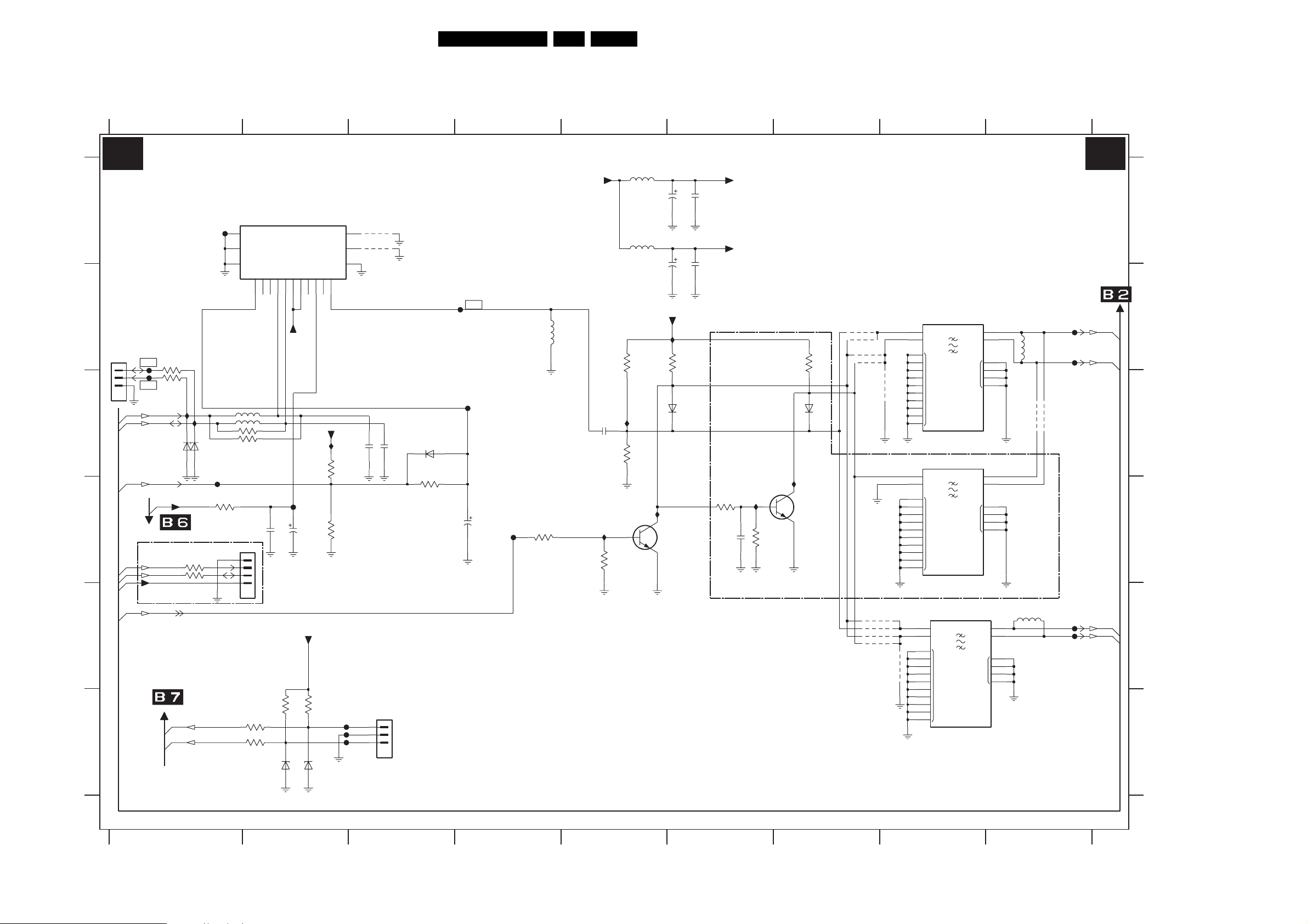
Circuit Diagrams and PWB Layouts
7. Circuit Diagrams and PWB Layouts
SSB: Tuner and IF
19LC4.31HU AB 7.
1 23456789
TUNER & IF
B1 B1
A
B
SERVICE
COMPAIR
1101
1
2
3
45
C
D
E
F
3139 123 6125.2
3112
18K
5102
6u8
5103
3107
6K8
I103
3109
2K2
7101
BC847BW
0V
6u8
5VSW_b
I105
0V
2101
100u
16V
2113
100u
16V
I102
3108
2K2
6104
1SS356
2102
10n
2103
10n
UV1318ST/AIH-MK3
3124
F102
100R
3125
F104
100R
I112
SCL
SDA
6101
BZX384-C6V8
RF_AGC
+VTUN
For ITV Only
3126
SCL
3127
SDA
+3V3STBY
TO/FROM iBOARD
SEL_IF_SDM
FROM SCALER
F101
I113
6102
BZX384-C6V8
F106
3105
1K0
100R
100R
UART_TX
UART_RX
1102
12
13
14
5107
5108
3102
3101
1103
1
2
3
4
3122 100R
TU
AGC1AS
2
NC
1V7
RES
RES
100R
100R
56
100R3123
6106
TUNER
SCL5SDA
4
3
2V6
5V3
2107
47n
NC16NC2
8
NC
2V6
5V3
5VSW_a
F107
2108
2u2
50V
3120 3121
10K
BZX384-C6V8
BZX384-C6V8
ADC
33V
10
11
95V7
0V
7V1
5VSW_a
+3V3STBY
10K
6107
15
16
17
IFOUT
I101
3103
10K
3106
RES
2104
22p
F115
F116
F117
RES
4115
RES
4116
SERVICE
UART
1107
2105
22p
45
+5VSW
F109
IF-TER
3111
22K
5101
390n
2106
10n
I104
F108
F105
6103
RES
3104
0R
2109
22u
16V
1
2
3
1 23456789
3113
22K
2114
1u0
5VSW_a
5VSW_b
I106
FOR I93 ONLY
3114
47K
3110
2K2
6105
1SS356
I110
7102
BC847BW
4102
*
4103
*
4104
4105
OFWK3955L
4109
4110
4111
4112
EUROPE & AP
PAL-MUTLI
ONLY
1104
OFWK3953L
38M9
OFWK9656L
I
ISWI
GND
38M
1106
40M4
*
7
O1
8
O2
11
12
NC
16
17
7
O1
8
O2
11
12
NC
16
17
*
O1
O2
NC
5106
7
8
11
12
16
17
2
I1
3
I2
4106
*
*
*
4113
1105
1
4
5
6
9
GND
10
13
14
15
18
*
2
I1
3
I2
1
4
5
6
9
GND
10
13
14
15
18
2
3
1
4
5
6
9
10
13
14
15
18
*
*
5105
RES
**
RES
4107
4108
VIF1
VIF2
SIF1
SIF2
F110
F111
F112
F113
G_16160_001.eps
030706
A
B
C
D
E
F
1101 B1
1102 A1
1103 D2
1104 B8
1105 C8
1106 E8
1107 F3
2101 A6
2102 A6
2103 A6
2104 C3
2105 C3
2106 C5
2107 D2
2108 D2
2109 D4
2113 A6
2114 D6
3101 C1
3102 C1
3103 C2
3104 C3
3105 D1
3106 D3
3107 B5
3108 B6
3109 C5
3110 B7
3111 D4
3112 D5
3113 D6
3114 D6
3120 F2
3121 F2
3122 F1
3123 F1
3124 B1
3125 C1
3126 D1
3127 D1
4102 B7
4103 B7
4104 B7
4105 B7
4106 C8
4107 C9
4108 C9
4109 E7
4110 E7
4111 E7
4112 E7
4113 E8
4115 A3
4116 A3
5101 B4
5102 A5
5103 A5
5105 B9
5106 E9
5107 C1
5108 C1
6101 C1
6102 C1
6103 C3
6104 C6
6105 C7
6106 F2
6107 F2
7101 D5
7102 D7
F101 A1
F102 B1
F104 C1
F105 C4
F106 D1
F107 D2
F108 B4
F109 D4
F110 B9
F111 B9
F112 E9
F113 E9
F115 F3
F116 F3
F117 F3
I101 C2
I102 B6
I103 C5
I104 D5
I105 D5
I106 D6
I110 D7
I112 C1
I113 C1
Page 20
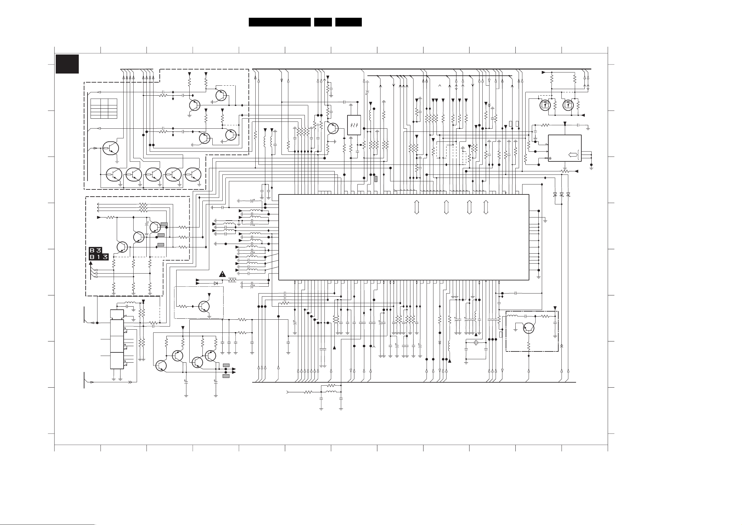
Circuit Diagrams and PWB Layouts
20LC4.31HU AB 7.
SSB: Hercules
123456789101112
B2
A
B
C
D
E
F
G
H
3139 123 6117.2
123456789101112
HERCULES
B15A
B15A
B15A
AUDIO PROCESSING
AUDOUTLSR
B5
HETV
(15W)
5K6
3203
3202
5K6
3206
5K6
3205
5K6
B5
AUDOUTLSL
PUMH7
7201-1
OUT_MUTE
B5
0V
7201-2 PUMH7
INTF_V_OUT
INTF_Y_OUT
INTF_U_OUT
+5VSW
/
R_OTC_SDTV
B_OTC_SDTV
G_OTC_SDTV
7219
RES
F210
SC2_OUT_SW
B7
14
15
4
SC2_CVBS_MON_OUT
B15A/B15B/B23
820R
820R
3250
100R
MTV
(5W)
10K
10K
16
VDD
MDX
B15A
SC1_L
SC2_L
SC1_R
SC2_R
3V9
7202-1
PUMH7
3V9
3228
3244
3289
I246
7209
BC847BW
7208
BC847BW
RES RES RES
3255
0R
3258
330R
5218
RES
2291
RES
6
G4
13
1
12
2
11
4X1
4X2
1
2
10
3
5
9
VEEVSS
8
7
3V9
2203
10u
16V
3256
0R
3259
330R
+5VSW
RES
3291
RES
3293
B15B
B15B
NC
NC
I289
2280
4u7
3201 100R
Const_L_OUT
Const_R_OUT
HER_SC2_AudioOutL
HER_SC2_AudioOutR
2281
3204 100R
F202
F201
F204
F203
3V9
7202-2
PUMH7
RES
RES
RES
7210
BC847BW
3257
0R
3260
330R
27K3292
150R3282
2290 4u7
47K
3294
5
2V5
7216-2
BC847BS
Const_L_OUT
Const_R_OUT
2201
I290
I292
4u7
2202
I293
7203-1
PUMH7
F220
F221
I218
420942084207
4206
3262 3265
3263
22K
3R9
7214
BCP69-25
2V1
3
4
+8VSW_TV
+8VSW_TV
*
3202
1u0
7204-2
BC857BS
1u0
3V9
3251
100R
3252
100R
3253
100R
+8VSW_TV
+5VSW
ES10.3B RESET (RESERVED)
3254
1K0
+3V3STBY
3
2
4
1V9
I294
7205-2
BC857BS
7203-2
PUMH7
I242
2V8
7216-1
BC847BS
2
2208
1u0
I291
22K
3264
50V
7204-1
BC857BS
+8VSW_TV
3V9
I243
I247
I248
BAS321
+1V8_B
2V
11
6
1V9
1
6201
*
3203
*
3205
+1V8_A
+1V8_B
7211
BC847BW
3R9
2V7
+8VSW_TV
7205-1
BC857BS
2230
GND
5206
2234 220n
5207
F227
3
7215
BCP69-25
2
4
2209
RES
4211
*
3206
100n
+3V3STBY
220n2235
+1V8_B
+1V8_A
+3V3STBY
+3V3STBY
+3V3STBY
+1V8_A
2u2
RES
2206
2205
F230
F231
I201
I202
4212
+5VSW
GND1
I221
5210
5211
2239 100n
5212
2240 220n
5213
2241
3280
1R0
3266
3267 5K6
2207
220n
+1V8_A
+1V8_B
2204
5204
5205
2232
2233
5208
2236
5209
2222
2243
220n
5K6
2258 10u
B1
B15A/B15B/B23
AV2_DMMI_SW
SEL_IF_SDM
+5VSW
+5VSW
100R
5201
5202
3296
10u
100n
RES
2228
2229
6.3V330u
F222
F223
F224
220n2231
100n
I220
10u 16V
I222
F225
220n
F226
220n2237
I223
220n2238
330u
6.3V
F228
I224
F229
100n2242
10u
16V
F234
F233
F232
SC1_CVI_DMMI_B_Pb_IN
SC1_CVI_DMMI_G_Y_IN
SC1_CVI_DMMI_R_Pr_IN
B15B/B23
B15B/B23
B15B/B23
CVBS_COMB
B1
SSIF
220n
2210
I219
7217
82
VP3
47
VP2
15
VP1
110
VDDP_3.3
69
VDDCOMB
3
VDDC4
124
VDDC3
100
VDDC2
117
VDDC1
96
VDDADC_1.8
4
VDDA3_3.3
94
VDDA2_3.3
88
VDDA1
93
VDDA_1.8
45
VCC8V
8V
2244 100n
2246
3268 100R
F235
SC1_FBL_IN_1
B15B/B23
B1
RF_AGC
MAIN_OUTR
MAIN_OUTL
680R
3207
100n2245
100n
2285
100n
100R3210
100R
10n2211
3208 100R
3209 100R
3211
I203
I285
I288
I283
I284
2V4
31
613637
626360
AGCOUT
AUDOUTLSL
AUDOUTHPL
AUDOUTLSR
AUDOUTHPR
Φ
VIDEO
SIGNAL
SSIF
AGC2SIF
AUDIOIN2L
AUDIOIN2R
AUDIOIN3L
46
53545657495034
I227
I254
2u2
50V
F236
2247
HDMI_AudioINL
DVI_D_AudioINL
DVI_D_AudioINR
HDMI_AudioINR
B12
B4/B22
B4/B22
B12
3286
+5VSW
B3
B15A
B15A
CVBS_COMB
3216 330R
SC1_L_RF_OUT
SC1_R_RF_OUT
330R
F206
F205
3215
2V2
100R
100R
*EMC
3213
3212
1n0
1n02216
*EMC
2214
I205
I204
F256
0V
33
AVL
SSIF
SWO
AUDOUTSL
AUDOUTSR
PROCESSOR
AUDIOIN4R
AUDIOIN5L
AUDIOIN5RBBCLIN
AUDIOIN3R
AUDIOIN4L
80
35
I255
F239
F240
F237
F238
2249
2248
RES
RES
HD_AudioINL
Analog_AudioINL
HD_AudioINR
B15A/B23
B15A/B23
B14/B22
3285
100R
2288
RES
100n
2218
2219
100n
1201
SFSKA
2213
4M5
RES
1V6
7206
BC857B
3214
680R
F255
8578
86
87
BO
RO
GO
REFO
REFIN
G
PBIN3
YIN3
79
I256
I257
I230
RES
RES
1n0
3271
2250
3270
+3V3STBY
Analog_AudioINR
B14/B22
0R
5217
RES
RES
I244
1K03217
CVBSO
PRIN3
I228
2287
RES
83
10u2251 25V
I206
2
GND
3
100K
RES
3218
2220
I207
44
43
PIP
DVBO
FMRO
C2C4CVBS2
BLKIN
84
59
I258
2252 100n
F241
AGC_Y_FB
SC2_AV3_C_IN
B18
B15A/B23
B15A
B3 /
16V
100u
2221
+5VSW
F250
SC1_CVBS_RF_OUT
1
I
F209
5203
SANDCASTLE
O
RES
RES
100R
47K3220
I208
3287
3288
3219
I298
F207
F208
66
21
AVL
EWD
IFVO
DVBO
FMRO
FBISO
HERCULES
TDA15021H/N1A11
C3
Y2
Y3
CVBS3
55585164201438
52
F248
I229
I231
100n
100n2253
2254
2286 100n
2255 100n
F243
F242
CVBS_COMB
SC2_Y_IN_1
SC1_CVBS_IN
B15B/B23
B15A/B23
B3
HOUT
67
CSY
CVBS4
16V
10u
2256
RES
3290
RES
3283
I209
48
HOUT
Y4
F244
100n
2257
RES
3284
SVO
IFVO
DECBG
DECDIG
I232
B4
I2SDI1
F212
106
CVBSI
I2SDI1
DECSDEM
DECV1V8
118
I233
10u2260
100n
2259
O
EHTO
32
3295 100K
2262 10u
B4
I2SDO1
105
I2SDO1
INSSW3
77
I259
39K
6n8
3281
2263
16V
B4
B5
I2SCLK
EXT_MUTE
100R3222
3V2
I210
104
103
102
I2SCLK
I2SDO2
IREF
PH1LF
27
17
16
I234
I235
I236
1K0
3273
3272 4K7
10V
I262
10V2265 1u0
470n
2264
B15B/B17
+3V3STBY
RC_OUT
I297
3225
10R
I211
3223
100R
I278
3227 4K7
I277
97
INT0
I2SWS
PH2LF
PLLIFRSECPLL
41
19
I237
220n
3274 390R
2267
100n
2266
B7
B7
TV_IRQ
TV_SC_COM
100p
I275
100R
2223
3226
+3V3STBY
4K7
3224
I212
RES
1u0
F211
2224
3V1
126
99
98
P0<0:5>
DVBAGC
SIFAGC
422930
1V9
I226
2268 2u2 50V
F251
B1
B17
+3V3STBY
PC-TV-LED
I274
3230 10K
3231 2K2
3229 4K7
0V
107
127
T1
RX
INT2T0INT1
DVBIN1
SIFIN1
SIFIN2
1V9
F252
SIF2
SIF1
B1
+3V3STBY
+3V3STBY
3K3
3233 3K3
3232
+3V3STBY
4216
4217
I273
3V2
128
108
109
TX
SCL
SDA
SWIO
DVBIN2
VGUARD
24
13
1V9
1V9
I264
100R
3275
F245
F254
F253
DMMI_RGB_SW
VIF2
VIF1
B1
B1
B15B/B23
/B23
B15B
/B23
B15B
B5
+3V3STBY
+3V3STBY
SOUND_ENABLE
4K7
4K7
SW|HW_I2C_SDA
SW|HW_I2C_SCL
3235
3234
+3V3STBY
4219
4218
RES
4204
FOR SERVICE
0V
3V2
3V2
114
122
112
113
111
PWM3
PWM2
PWM1
PWM0
TPWM
P1<0:7>
VREF_POS_HPR
VREF_POS_LSL
VIFIN2
VREF_NEG_HPL+HPR
VREF_NEG_LSL+HPL
VIFIN1
86957
25
I238
2269 470u 16V
2270 100n
3276 75R
5214 1m0
+3V3STBY
B15B
B15A
B8
B17
B9,B17
+3V3STBY
4K73236
RES
RES
4205
3237
F213
123
PWM4
VREF_POS_LSR+HPR
918990
I239
100u 16V
100n
2271
2272
+3V3STBY
RES
8p2
2275
KEYBOARD
+3V3STBY
STATUS_1
STATUS_2
1%
F214
F215
+3V3STBY
3240 1K0
LS|PDP_DVB_SEMISTANDBY
I241
4K73299
100R
3n3
100R
3238
2226
3239
I214
0V
0V
I225
I213
115
116
119
120
39
ADC3
ADC1
ADC0
ADC2
QSSO
P2<0:5>
P3<0:3>
VREFAD
VREFAD_NEG
VREFAD_POS
VSC
26
10
1V4
I240
F246
150n2274
5216
2273 220n
1202
24M576
XTALIN
XTALOUT
11
1V4
8p2
2276
UIN
RES
2282
F262
RES
INT_U_IN
B18
B9/B20
B6/B15B/B23
SC_STANDBY
1n0
2225
3241 100R
10K
I215
3242
F216
657175
SVM
AMOUT
AUDEEM
VIN
YIN
YSYNC
727473
70
F257
2277 100n
1K5
RES
RES
2284
2283
3277
F263
F264
INT_V_IN
INT_Y_IN
B18
B18
B3/B18
B18
B3
VSYNC
INTF_V_OUT
INTF_U_OUT
+3V3STBY
I271
I272
I270
RES
220K
3245
2293
3243 4K7
POWER_DOWN_BOLTON_P50
23
22
76
VDRB
VDRA
VOUT
UOUT
SWO1
INSSW2
VSSP2
VSSCOMB
VSSC4
VSSC3
VSSC2
VSSC1|P
VSSADC
VSSA1
GNDIF
2292
I265
100n
2278
5215
47u
I266
INTF_Y_OUT
B18
+3V3SW
B3/B15B/B23
RES
4220
7220
BSN20
P50_LINE_ITV_IR_SW_RST
2227
1n0
NVM_WP_HERC
F218
3V2
3247
7
100R
F217
6
2V9
3248
5
100R
2V8
F258
I269
I217
YOUT
F247
1
68
GND1
2
125
101
121
95
12
92
GNDA
81
GND3
40
GND2
18
GND1
28
F249
I267
3278
27p
68K
8V
7218
BC847BW
0V
SECAM CIRCUIT
3279
100R
(RESERVED)
I268
Y_NOTCH
B7
WC
SCL
3297
3K3
3221
4K73249
100n
2279
4221
3
RES
7221
BSN20
+3V3STBY
Φ
(2Kx8)
EEPROM
3246
BAT54 COL
6205
6204 BAT54 COL
+8VSW_TV
POWER_DOWN
B6
3298
3K3
RES
2312
3261
1
2212
100n
3V2
7207
84
M24C16-WMN6
ADR
4K7
BAT54 COL
6206
IRQ_DIGITAL
B15B/B23
G_16210_002.eps
B8
SCL
RES
+3V3SW
0
1
2SDA
F219
+3V3STBY
SDA
1201 B7
1202 G10
2201 A3
2202 B3
2203 D2
2204 C5
2205 G4
A
B
C
D
E
F
G
H
2206 G4
2207 F5
2208 G4
2209 G4
2210 B5
2211 B6
2212 B12
2213 B7
2214 B6
2216 B6
2218 A7
2219 A7
2220 B7
2221 A7
2222 E5
2223 B8
2224 C8
2225 B10
2226 C10
2227 B11
2228 C5
2229 C5
2230 D4
2231 D5
2232 D5
2233 D5
2234 D4
2235 D4
2236 D5
2237 D5
2238 E5
2239 E5
2240 E5
2241 E5
2242 E5
2243 E5
2244 E5
2245 E5
2246 F5
2247 F6
2248 G6
2249 G6
2250 F7
2251 F7
2252 F7
2253 F7
2254 F7
2255 F7
2256 F8
2257 F8
2258 G5
2259 G8
2260 F8
2262 G8
2263 F8
2264 G8
2265 G8
2266 G8
2267 F8
2268 G8
2269 F9
2270 F9
2271 F9
2272 F9
2273 F10
2274 F10
2275 G9
2276 G10
2277 F10
2278 F11
2279 F11
2280 A3
2281 B3
2282 F10
2283 F10
2284 F10
2285 F6
2286 F7
2287 H7
2288 H6
2290 F3
2291 F2
2292 E11
2293 C10
3201 A3
3202 A4
3203 A4
3204 B3
3205 B4
3206 B4
3207 B6
3208 B6
3209 B6
3210 B6
B8
1
2
3
160106
3211 B6
3212 B6
3213 B6
3214 B7
3215 B6
3216 A6
3217 B7
3218 B7
3219 B7
3220 B7
3221 A11
3222 B8
3223 B8
3224 B8
3225 B8
3226 B9
3227 C8
3228 D2
3229 C9
3230 B9
3231 B9
3232 B9
3233 B9
3234 B9
3235 B9
3236 B9
3237 C9
3238 B10
3239 C10
3240 B10
3241 B10
3242 C10
3243 C10
3244 D2
3245 C10
3246 C11
3247 B11
3248 C11
3249 B11
3250 D2
3251 D3
3252 D3
3253 D3
3254 F3
3255 E2
3256 E2
3257 E3
3258 E2
3259 E2
3260 E3
3261 A12
3262 F3
3263 F3
3264 F4
3265 F4
3266 F4
3267 F4
3268 F5
3270 F7
3271 F7
3272 F8
3273 F8
3274 F8
3275 F9
3276 F9
3277 F10
3278 F11
3279 G11
3280 E4
3281 F8
3282 F3
3283 B8
3284 B8
3285 G6
3286 H6
3287 B7
3288 B7
3289 D2
3290 B8
3291 F2
3292 F2
3293 G2
3294 G2
3295 F8
3296 B5
3297 A11
3298 A12
3299 B10
4204 C9
4205 C9
4206 F3
4207 E2
4208 E2
4209 E3
4211 A4
4212 B4
4216 B9
4217 B9
4218 B9
4219 B9
4220 A11
4221 A12
5201 B5
5202 B5
5203 B7
5204 D5
5205 D5
5206 D4
5207 D4
5208 D5
5209 D5
5210 D5
5211 E5
5212 E5
5213 E5
5214 G9
5215 F10
5216 F10
5217 H7
5218 F2
6201 E4
6204 C11
6205 C11
6206 C12
7201-1 B1
7201-2 C2
7202-1 C2
7202-2 C3
7203-1 C3
7203-2 C3
7204-1 A4
7204-2 A3
7205-1 B4
7205-2 B4
7206 B6
7207 B12
7208 D2
7209 D2
7210 D3
7211 F4
7214 G3
7215 G4
7216-1 G3
7216-2 G3
7217 C6
7218 F11
7219 F2
7220 A11
7221 A12
F201 B2
F202 B2
F203 B3
F204 B3
F205 B6
F206 B6
F207 C7
F208 C7
F209 B7
F210 F2
F211 C9
F212 C8
F213 C10
F214 B10
F215 B10
F216 C10
F217 B11
F218 B11
F219 C12
F220 D3
F221 D3
F222 D5
F223 D5
F224 D5
F225 D5
F226 D5
F227 D4
F228 E5
F229 E5
F230 G4
F231 G4
F232 F5
F233 F5
F234 F5
F235 F5
F236 F6
F237 F6
F238 F6
F239 F6
F240 F6
F241 G7
F242 G7
F243 G7
F244 F8
F245 F9
F246 F10
F247 D11
F248 F8
F249 E11
F250 A7
F251 G9
F252 G9
F253 G9
F254 G9
F255 C7
F256 B6
F257 E10
F258 C11
F262 F10
F263 F10
F264 F10
I201 A5
I202 B5
I203 B6
I204 B6
I205 B6
I206 A7
I207 C7
I208 B7
I209 C8
I210 C8
I211 B8
I212 B9
I213 C10
I214 C10
I215 C10
I217 C11
I218 D3
I219 C5
I220 D5
I221 D5
I222 D5
I223 D5
I224 E5
I225 C10
I226 F8
I227 F6
I228 F7
I229 F7
I230 F7
I231 F7
I232 F8
I233 F8
I234 F8
I235 F8
I236 F8
I237 F8
I238 F9
I239 F9
I240 F10
I241 B10
I242 F4
I243 C4
I244 B7
I246 D2
I247 D4
I248 D4
I254 F6
I255 F6
I256 E7
I257 E7
I258 E7
I259 F8
I262 F8
I264 F9
I265 F10
I266 F10
I267 F11
I268 G11
I269 C11
I270 B11
I271 B10
I272 B10
I273 C9
I274 A9
I275 A9
I277 C8
I278 C8
I283 B6
I284 B6
I285 B6
I288 B6
I289 A3
I290 A3
I291 A4
I292 B3
I293 B3
I294 B3
I297 B8
I298 C7
Page 21
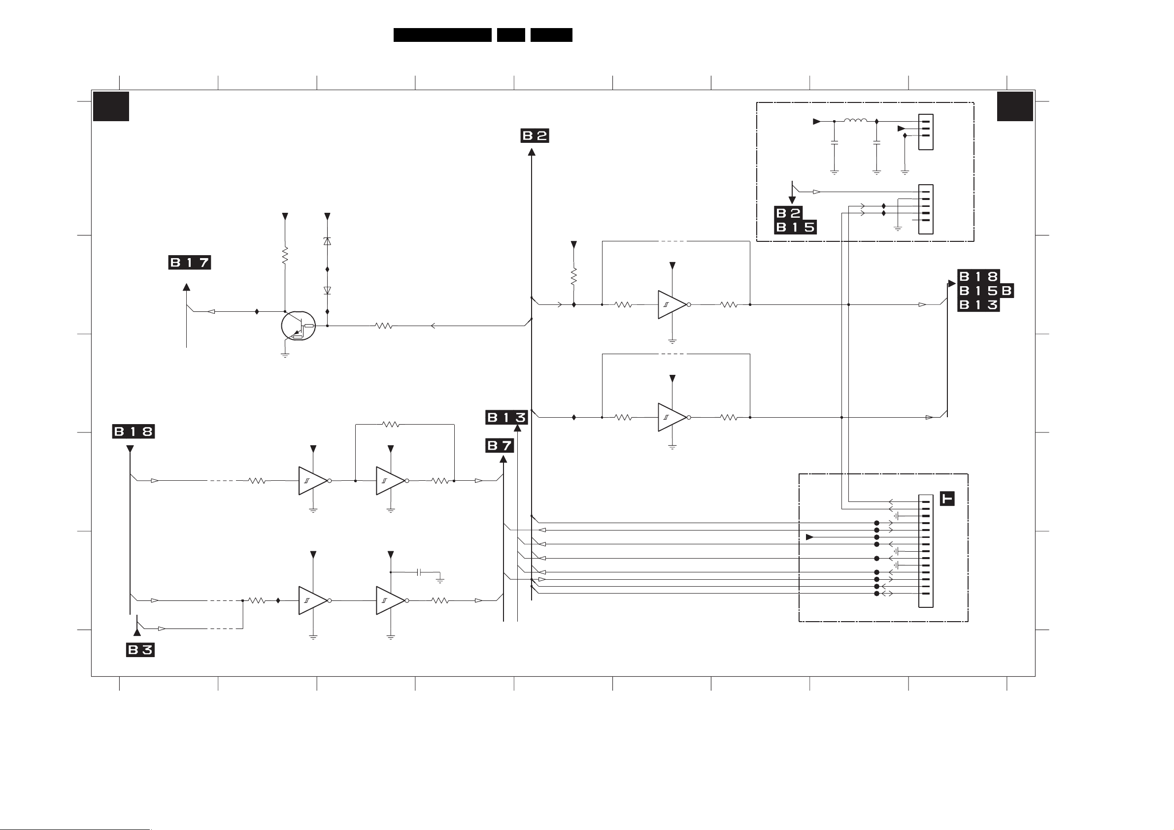
SSB: Sync Interface
123456789
Circuit Diagrams and PWB Layouts
21LC4.31HU AB 7.
B3 B3
SYNC INTERFACE
FOR ITV ONLY
+12VSW
2447
10p
5431
I451
2448
10p
+5V
I452
1441
1
2
3
45
B3B-PH-SM4-TBT(LF)
A
1440
1
2
3
4
5
67
BM05B-SRSS-TBT
1442
1
2
3
4
5
6
7
8
9
10
11
12
13
14
16
15
BM14B-SRSS-TB
TO/FROM 1000 OF
B
C
D
E
TO SIDE CONNECTORS
COL_HREF
COL_VA
Vsync_SDTV
4440
4441
4439
RES
LED_SEL
I454
3458
3461
100R
+3V3STBY
3431
1K0
7430
PDTC114ET
0V
7436-3
74LVC14APW
5
I455
13
+3V3SW
14
7
+3V3SW
74LVC14APW
14
7
+5VSW
3V1
7436-6
6430
BZX384-C2V7
I453
6431
1N4148
I430
6
74LVC14APW
12
3432
9
11
+3V3SW
+3V3SW
7436-5
RES
3463
RES
7436-4
74LVC14APW
14
7
14
7
8
2449
100n
10
P50_LINE_ITV_IR_SW_RST
3459
H_1FH
100R100R
3462
V_1FH
100R
SC1_CVBS_RF_OUT
I449
&
+3V3STBY
3451
4K7
I443
HOUT Hsync_SDTV
VSYNC
I440
CVBS_COMB
INT_OTC
R_OTC_SDTV
G_OTC_SDTV
B_OTC_SDTV
RESET_FLASH
SCL
SDA
74LVC14APW
3453
100R
3455
1
3
7436-1
4436
RES
+3V3SW
14
7
4437
RES
+3V3SW
74LVC14APW
14
7
7436-2
3454
2
100R
3456
4
100R100R
+3V3SW
I450
Vsync_SDTV
FOR OTC ONLY (1000pg TEXT)
F404
F405
F406
F407
F408
F409
F410
F411
F412
A
B
C
D
E
1440 A9
1441 A9
1442 D9
2447 A8
2448 A8
2449 E4
3431 B2
3432 B3
3451 B5
3453 B6
3454 B7
3455 C6
3456 C7
3458 D2
3459 D4
3461 E2
3462 E4
3463 C3
4436 B6
4437 C6
4439 E1
4440 D2
4441 E2
5431 A8
6430 B3
6431 B3
7430 B2
7436-1 B6
7436-2 C6
7436-3 D2
7436-4 D3
7436-5 E3
7436-6 E3
F404 D8
F405 D8
F406 E8
F407 E8
F408 E8
F409 E8
F410 E8
F411 E8
F412 E8
I430 B3
I440 C5
I443 B5
I449 A8
I450 A8
I451 A8
I452 A8
I453 B3
I454 B2
I455 E2
3139 123 6117.2
G_16210_003.eps
160106
123456789
Page 22
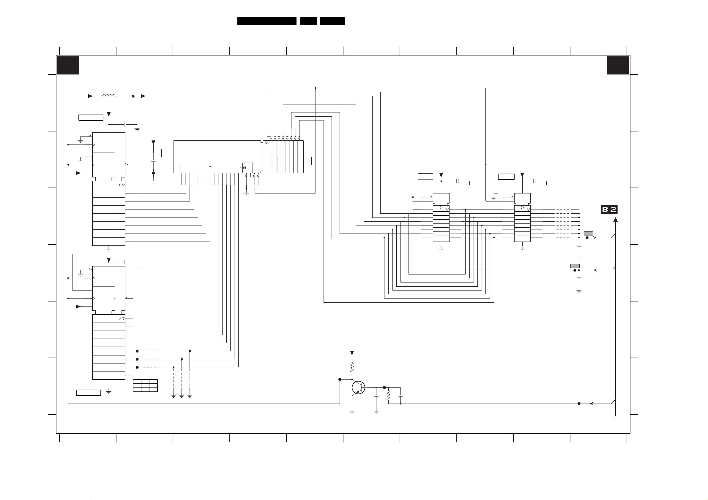
Circuit Diagrams and PWB Layouts
SSB: Audio Delay Line (PDP Only)
22LC4.31HU AB 7.
12345678910
B4 B4
AUDIO DELAY LINE (LIPSYNC) (FOR PDP SETS ONLY)
+5VSWI
1u05501
F501
+5VD
A
+5VD
B
C
D
E
F
COUNTER
+5VD
+5VD
COUNTER
7501
M74HC590T
14
13
2V3
12
11
2V3
10
5V3
14
13
12
5V3
11
2V3
10
5V3
7503
M74HC590T
EN3
C2
G1
1+
CT=0
EN3
C2
G1
1+
CT=0
VCC
CTR8
(CT=255)Z4
GND
+5VD
16
VCC
CTR8
(CT=255)Z4
GND
2501 100n
16
2D 3
8
2D 3
8
2V5
7502
+5VD
2502
9
4
4
100n
5V3
F502
15
1
2V6
2
2V6
3
2V6
4
2V6
5
2V6
6
2V6
7
2V6
100n2503
5V3
9
15
1
2
3
I503
4
4501
I504
5
4502
I505
6
4503
*
7
LCD PDP
*
4503
NYY
4504
N
CY62256LL-70ZC
5V3
2V6
2V6
2V6
2V6
2V6
2V6
2V6
*
4504
RAM
32kx8
0
2425261234
21
23
I506
I507
RES
RES
4506
4505
0
A
32k-1
1110987654321
5
8910
6
7
2EN
14
13
12
222827
11121315161718
A
A,1D
2C1
G2
20
2V3
19
14
+5VD
2505
100n
20
5V3
1
EN
11
C1
2
1D
3
4
5
6
7
8
9
19
18
17
16
15
14
13
12
10
4507
4508
4509
4510
4511
4512
4513
4514
RES
RES
RES
RES
RES
RES
RES
F504
2V6
F505
F503
2506
330p
2507
470p
I501
2V3
+5VD
3501
470R
BC847BW
7504
0V2
I502
2508
82p
3502
47K
2V3
2509
82p
LATCH
7505
74HC573PW
1
11
2V6
2
3
4
5
6
7
8
9
EN
C1
1D
5V3
+5VD
2504
100n
20
2V3
19
18
17
16
15
14
13
12
10
LATCH
7506
74HC573PW
2V5
2V5
2V5
2V5
2V5
2V5
2V5
I2SDI1
I2SDO1
I2SCLK
A
B
C
D
E
F
2501 A2
2502 B2
2503 D2
2504 B8
2505 B9
2506 C10
2507 D10
2508 F6
2509 F7
3501 F6
3502 F6
4501 E2
4502 F2
4503 F2
4504 F2
4505 F3
4506 F3
4507 C9
4508 C9
4509 C9
4510 C9
4511 C9
4512 C9
4513 C9
4514 C9
5501 A1
7501 A1
7502 B3
7503 F1
7504 F6
7505 B7
7506 B8
F501 A2
F502 B2
F503 C10
F504 D10
F505 F10
I501 F5
I502 F6
I503 E2
I504 E2
I505 F2
I506 E3
I507 E3
3139 123 6117.2
123456789
G_16210_004.eps
10
160106
Page 23
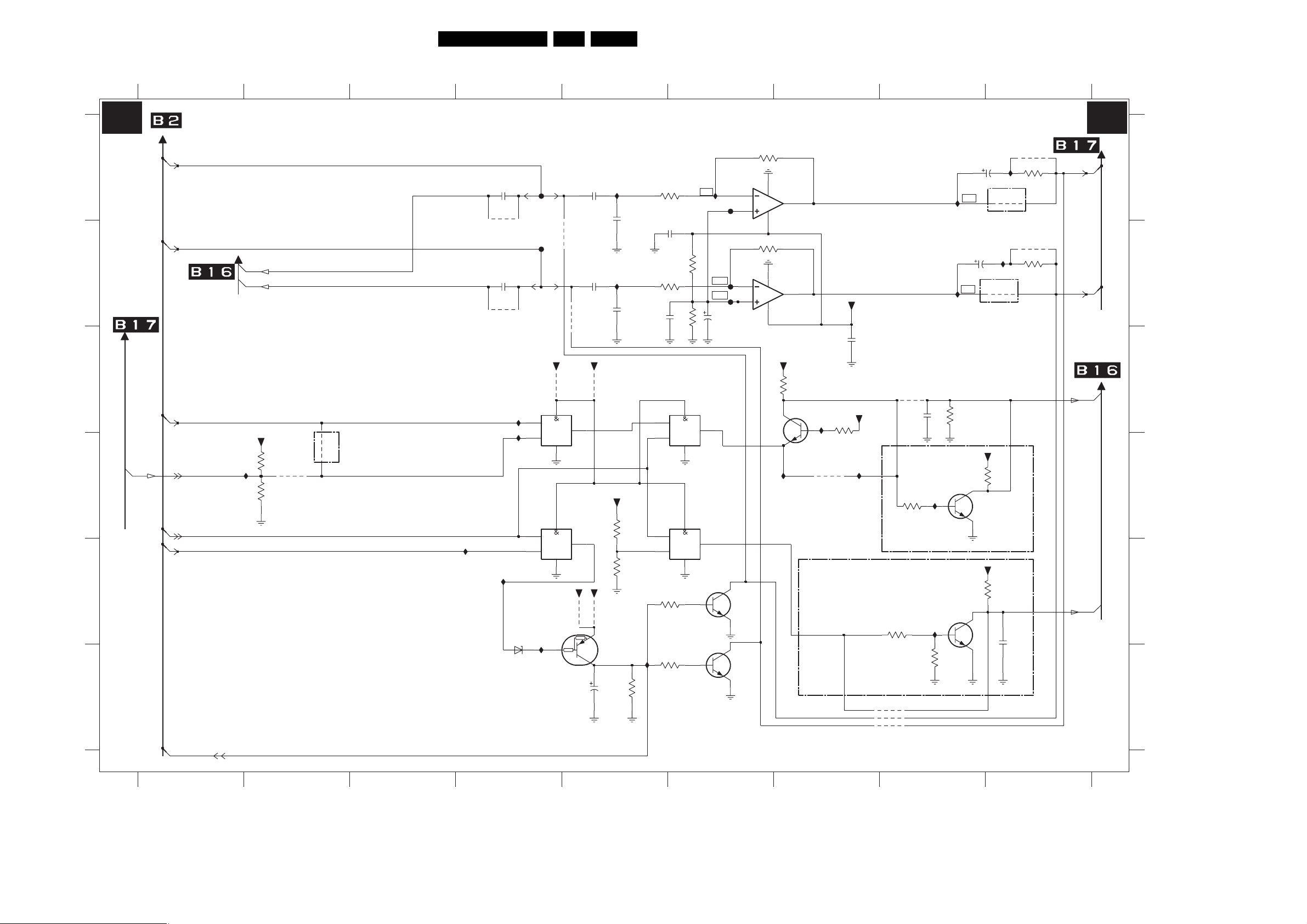
Circuit Diagrams and PWB Layouts
23LC4.31HU AB 7.
SSB: Audio Processing
123456789
FROM HERCULES
B5 B5
A
B
C
D
E
F
OUT_MUTE
3139 123 6117.2
AUDIO PROCESSING
AUDOUTLSL
AUDOUTLSR
AUDIO-L
AUDIO-R
SOUND_ENABLE
HP_DET_R_DC
POWER_DOWN
EXT_MUTE
+5VSW
I620
3626
10K
3627
22K
4613
ITV ONLY
4601
*
RES
I613
2616
2u2
4618
*
RES
2617
2u2
4619
*
RES
I614
BZX384-C3V3
7602-1
74HC08PW
I606
I607
6601
F601
F602
1
2
9
10
4611
+3V3SW
4616
14
7
14
7
7605
PDTA143ET
I615
5V
RES
RES
4612
+3V3STBY
3
7602-3
74HC08PW
8
+5V
RES
4621
2619
47u
6.3V
2603
1u0
2608
1u0
4617
3V3
+5VSW
4620
5V2
RES
I610
+5V
0V
I608
3623
47K
HPIC_LIN
2604
470p
HPIC_RIN
2609
470p
3628
RES
3629
RES
I617
3604
22K
2605
1u0
3609
22K
2610
1u0
7602-2
74HC08PW
4
5
12
13
3630
470R
3631
470R
3610
100K
3611
100K
14
14
7
7
I618
7602-4
74HC08PW
11
F603
F604
F605
2611
100u
16V
6
0V
0V
7606-1
BC847BS
7606-2
BC847BS
2V6
2
2V6
3
84
3612 22K
2V6
6
2V6
5
84
3625
3K3
7601-1
TS482IDT
5V3
7601-2
TS482IDT
5V3
I612
22K3605
2V6
2V6
+5VSW
3V4
1
7
BC847BW
I611
3V2
7607
4606
*
FOR LCD 37" - 50"
+5VSW
3615
10K
2614
100n
+3V3SW
I621
HPIC_LOUT
HPIC_ROUT
3.2 TO 4.3V
4602
*
FOR LARGE SCREEN 37" - 50"
3620
10K
4603
4614
RES
*
4615
RES
*
*
3619
10K
3621
RES
I616
2613
1u0
BC847BW
I619
BC847BW
7604
3618
22K
7603
470u 16V
I602
2618
470u
I603
+3V3STBY
+3V3STBY
2615
16V
**
4609
3632
I604
39R
4604
**
RES
4610
I605
3633
39R
4605
RES
SOUND_ENABLE_1
3617
1K0
3616
1K0
2612
1u0
10V
HP_LOUT
HP_ROUT
POR_AUDIO
G_16210_005.eps
160106
A
B
C
D
E
F
2603 A5
2604 A5
2605 B6
2608 B5
2609 B5
2610 B5
2611 B6
2612 E9
2613 C8
2614 C7
2615 A9
2616 A4
2617 B4
2618 B8
2619 F5
3604 A6
3605 A6
3609 B6
3610 B6
3611 B6
3612 B6
3615 C7
3616 E9
3617 D9
3618 C8
3619 D8
3620 E8
3621 F8
3623 F5
3625 C6
3626 D2
3627 D2
3628 D5
3629 E5
3630 E6
3631 F6
3632 A9
3633 B9
4601 D2
4602 C8
4603 F8
4604 A9
4605 B9
4606 D7
4609 A9
4610 B9
4611 B4
4612 B5
4613 D2
4614 F8
4615 F8
4616 C4
4617 C5
4618 A4
4619 B4
4620 E5
4621 E5
6601 E4
7601-1 A7
7601-2 B7
7602-1 C4
7602-2 C5
7602-3 D5
7602-4 D6
7603 E8
7604 D8
7605 E4
7606-1 E6
7606-2 F6
7607 D7
F601 A4
F602 B4
F603 A6
F604 B6
F605 B6
I602 A8
I603 B8
I604 A9
I605 B9
I606 C4
I607 C4
I608 A5
I610 B5
I611 C7
I612 D7
I613 E3
I614 E4
I615 E4
I616 E8
I617 F5
I618 A6
I619 D8
I620 D2
I621 D7
123456789
Page 24
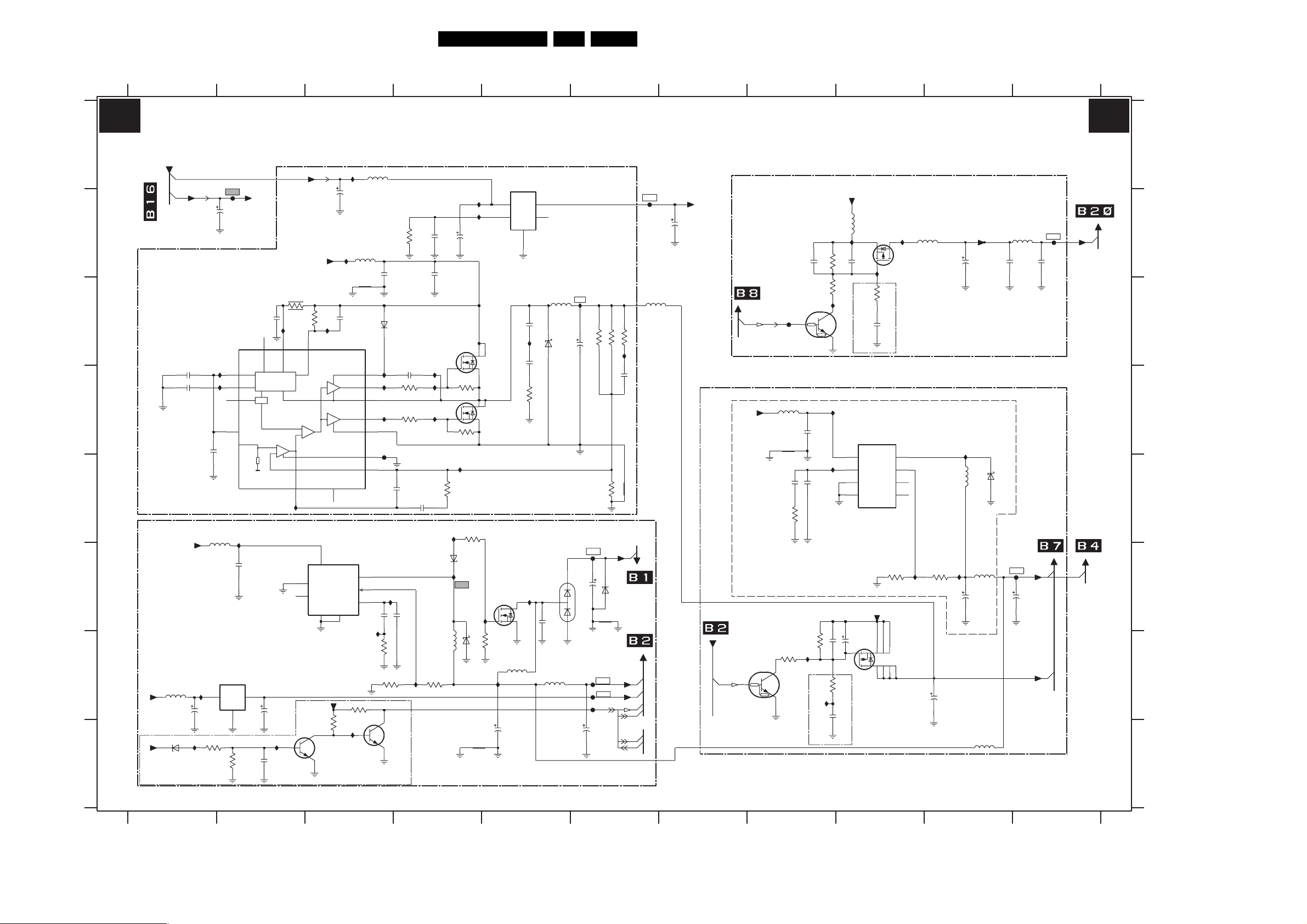
Circuit Diagrams and PWB Layouts
24LC4.31HU AB 7.
SSB: DC-DC Converter
1234567891011
B6 B6
DC-DC CONVERTER
A
B
C
D
E
F
G
H
3139 123 6117.2
+5V
2702
100n
SIG_GND2
I711
I712
F701
+12VSW
2704
16V
10u
+12VSW
3718
2719
100n
10R
I714
15
VCC
I722
3
OCSET
COMP
5
9
7710
L6910
1
4
2
8
VREF
SS
OSC
EAREF
SIG_GND2
PGOOD
Monitor
Protection & Ref
OSC
+12VSW
FROM TOP CONNECTORS
100n2717
2718
100n
SIG_GND2
FOR 37"-50" LARGE SCREEN
SUPPLY TO TUNER & HERCULES
+12VSW
5730
I731
10u
2730
16V22u
SUP_GND1
SUP_GND1
COM
OUTIN
2
3741
1K5
7738
L78M08CDT
3
5738
120R
PDZ8.2-B
I740
I702
2738
1
16V47u
3740
1K5
+12VSW +8VSW_TV
+12VSW 6740
2739
47u
I741
2741
220n
16V
7730
L5973D
3
2
+3V3STBY
INH
SYNC
FOR 37"-50" LARGE SCREEN
123456789
3719
680R 1n0
I715
NC
16
8
VREFVCC
Φ
GND GND_HS
7
SUP_GND1
3742
15K
7741
BC847BW
I706
2706
10u 16V
5709
I710
2720
BOOT
HGATE
PHASE
LGATE
PGND
GND
VFB
6
OUT
FB
COMP
9
SUP_GND1
SUP_GND1
3743
22K
I742
5704
I709
I708
2709
27083709
6K8
RES
10u
22u 16V
6717
BAS316
2721
12
I716
11
3720
I718
10
14
I720
13
F717
7
SIG_GND2
6
2722
1n0
2723
1
5
I705
4
2734
2733
22n
220p
I701
3736
4K7
SUP_GND1
3732
1%1K0
7742
BC847BW
I732
100n
2R2
3733
27112710
22u
SUP_GND2SUP_GND2
I717
I719
2R23721
I721
47n
6734
5733
33u
3K3
16V
I762
1%
2
3701
10K
4
3702
10K
I723
3722
2K7
3734
100R
BZX384-C6V8
I733
6733
SUP_GND1
16V47u
7
1
5
3
I734
SS14
SUP_GND1
1
2
8
7711-1
SI4922DY
6
7711-2
SI4922DY
2N7002
3735
1K0
I736
SUP_GND1
7708
LF33CPT
CTRL NC
2724
1n0
2725
1n0
3723
10R
SUP_GND2
7735
SUP_GND1
5735
100u
2731
COM
I724
16V470u
3
OUTIN
I735
SUP_GND1
5
4
NC
SS246718
BAV99
2735
680p
5737
10u
5717
10u
6735
I725
2726
SUP_GND2
SIG_GND2
2736
22u
35V
SUP_GND1
SUP_GND1
5V2
8V
1%
3K3
15K3724
16V
470u
3725
3727
1%
1K0
F736
+VTUN
6736
BZX384-C33
TO HERCULES CELL
F737
F738
F743
POWER_DOWN
2737
470u
16V
F710
1K2
3726
I726
10n
2727
32V9
TO TUNER CELL
+5VSW
B5
B7
B16
5713
3u3
+3V3STBY
2716
470u
16V
FROM HERCULES
FOR 26"-42" SCREEN
FROM SCALER
PANEL-PWR-CTL
SUPPLY TO SCALER
+12VSW
GND
SUP_GND3
0V
SC_STANDBY
3V1
7755
PDTC114ET
(0V)
F755
0V6
5752
10u
2753
22u 16V
SUP_GND3
2763
22n
3737
4K7
SUP_GND3
3759
12K
7756
PDTC114ET
I748
3750
22K
2756
220p
RES
RES
2749
3758
15K
I760
I764
I758
SUP_GND3
I704
RES
2750
3755
10K
3761
100R
2761
1u0
25V
I756
+12VSW
5756
SI2301BDS-T1-E3
11V5
2751
4u7
I747
RES
7752
L5970D
8
VCC
4
COMP5FB
3
INH
7
GND
SUP_GND3
3V2
2762
16V22u
4
7754
2
1
6V8
3760
100R
2760
1u0
25V
SYNC
VREF
+3V3STBY
123
567
OUT
1K0
SS = 4V9
I757
3
3753
1%
7758
SI4423DY
8
3V2
5757
120R
PAN_VCC
2752
47u 16V
120R
2700
RES
5700
2701
100p
F700
RES
3754
1%
100u 16V
I754
SUP_GND3
2759
I755
5753
220u
SUP_GND3
2757
470u 16V
5754
10u
5751
10u
6751
SS14
TO SCALER CELL
F754
+5VSWI
5V4
2758
470u
+3V3SW
16V
1
2
6
I753
1V2
3K3
10 11
TO PACIFIC3
LVDS_VCC
11V5
TO LIPSYNC
G_16210_006.eps
160106
A
B
C
D
E
F
G
H
2700 B11
2701 B11
2702 D1
2704 B2
2706 A3
2708 B4
2709 B4
2710 B4
2711 B4
2716 B7
2717 D1
2718 D1
2719 C2
2720 C3
2721 D4
2722 E4
2723 E4
2724 C5
2725 C5
2726 C5
2727 D6
2730 F2
2731 H5
2733 F4
2734 F3
2735 F5
2736 F6
2737 H6
2738 G1
2739 G2
2741 H2
2749 B8
2750 F9
2751 B9
2752 B10
2753 D8
2756 E8
2757 F10
2758 F11
2759 G10
2760 C9
2761 G9
2762 G9
2763 E8
3701 D4
3702 D4
3709 B4
3718 C2
3719 C3
3720 D4
3721 D3
3722 E4
3723 D5
3724 C6
3725 C6
3726 C6
3727 E6
3732 G3
3733 G4
3734 E4
3735 G5
3736 G3
3737 E8
3740 H2
3741 H2
3742 H3
3743 G3
3750 G8
3753 F9
3754 F10
3755 B9
3758 C8
3759 G8
3760 C9
3761 G9
5700 B11
5704 A3
5709 B3
5713 C6
5717 C5
5730 E2
5733 G4
5735 G5
5737 G5
5738 G1
5751 H10
5752 D8
5753 E10
5754 F10
5756 B9
5757 B10
6717 C3
6718 C5
6733 G4
6734 F4
6735 F5
6736 F6
6740 H1
6751 E10
7708 A5
7710 C2
7711-1 C4
7711-2 D4
7730 F2
7735 F5
7738 G2
7741 H3
7742 H3
7752 D9
7754 B9
7755 C8
7756 G8
7758 G9
F700 B11
F701 B2
F710 B6
F717 D3
F736 F6
F737 G6
F738 G6
F743 G6
F754 F11
F755 C8
I701 F3
I702 G1
I704 G8
I705 F3
I706 A3
I708 B4
I709 B4
I710 B3
I711 D2
I712 D2
I714 C2
I715 C3
I716 D3
I717 D4
I718 D3
I719 D4
I720 D3
I721 D4
I722 E2
I723 E4
I724 C5
I725 C6
I726 C6
I731 E2
I732 G4
I733 F4
I734 F4
I735 F5
I736 G5
I740 H1
I741 H2
I742 H3
I747 B9
I748 G8
I753 F9
I754 F10
I755 D10
I756 B9
I757 B9
I758 E8
I760 C8
I762 E4
I764 D8
Page 25

Circuit Diagrams and PWB Layouts
B
C
SSB: Diversity Tables B1-B6
B01
25LC4.31HU AB 7.
B05 B06
Item nr.
1152 TUN V+U PLL IEC BGHIL B
3163 RST SM 0603 100R PM5 COL
3164 RST SM 0603 100R PM5 COL
5152 FXDIND SM 1008 1U PM5 COL R
5157 FXDIND 0603 100MHZ 600R COL R
5158 FXDIND 0603 100MHZ 600R COL R
Description
EU non DVB
EU DVB
TUNER UV1318SD/A CP H N-4
FXDIND SM 1008 6U8 PM5 COL R
B02
Item Nr.
2203 319803041090 ELCAP SM 16V 10U PM20 COL R
2244 319803571040 CER2 0402 Y5V 16V 100N COL
2245 319803571040 CER2 0402 Y5V 16V 100N COL
2246 319803571040 CER2 0402 Y5V 16V 100N COL
2280 202055200005 CER2 0603 X5R 6V3 4U7 PM10 R
2281 202055200005 CER2 0603 X5R 6V3 4U7 PM10 R
2289 319802131510 RST SM 0603 150R PM5 COL
2290 222224059872 CER2 0805 Y5V 10V 4U7 P8020 R
2291 319803571040 CER2 0402 Y5V 16V 100N COL
3250 319803101010 RST SM 0402 100R PM5 COL
3251 319803101010 RST SM 0402 100R PM5 COL
3252 319803101010 RST SM 0402 100R PM5 COL
3253 319803101010 RST SM 0402 100R PM5 COL
3255 319803190010 RST SM 0402 JUMP. 0R05 COL
3256 319803190010 RST SM 0402 JUMP. 0R05 COL
3257 319803190010 RST SM 0402 JUMP. 0R05 COL
3258 319803101020 RST SM 0402 1K PM5 COL
3259 319803101020 RST SM 0402 1K PM5 COL
3260 319803101020 RST SM 0402 1K PM5 COL
3282 319802131510 RST SM 0603 150R PM5 COL
3294 319803104730 RST SM 0402 47K PM5 COL
3296 319803101010 RST SM 0402 100R PM5 COL
4206 319802190020 RST SM 0805 JUMP. 0R05 COL R
4218 319803190010 RST SM 0402 JUMP. 0R05 COL
4219 319803190010 RST SM 0402 JUMP. 0R05 COL
5218 242254945333 IND FXD 1206 EMI 100MHZ 120R R
6206 319801010660 DIO SIG SM BAT54 SOD323 COL R
7208 319801042310 TRA SIG SM BC847BW (COL) R
7209 319801042310 TRA SIG SM BC847BW (COL) R
7210 319801042310 TRA SIG SM BC847BW (COL) R
7217 935280215557 IC SM TDA15031H/N1C91 (PHSE)Y
935280366557 IC SM TDA15021H/N1C91 (PHSE) Y
935280367557 IC SM TDA15011H/N1CD0 (PHSE) Y
7219 319801071090 IC SM 74HC4053D (COL) R
/93 China
AP 10pg TXT
EU 10pg TXT
EU 10pg TXT DVB
EU 1000pg TXT
EU 1000pg TXT DV
Description
B03
Item Nr.
2612 319801741050 CER2 0603 Y5V 10V 1U COL
2613 319801741050 CER2 0603 Y5V 10V 1U COL
2616 202055200035 CER2 0603 X5R 6V3 2U2 PM10 R
2617 202055200035 CER2 0603 X5R 6V3 2U2 PM10 R
2619 319803024790 ELCAP SM 6V3 47U PM20 COL R
3615 319803101030 RST SM 0402 10K PM5 COL
3616 319803101020 RST SM 0402 1K PM5 COL
319803190010 RST SM 0402 JUMP. 0R05 COL
3617 319803101020 RST SM 0402 1K PM5 COL
3618 319803102230 RST SM 0402 22K PM5 COL
3619 319803101030 RST SM 0402 10K PM5 COL
3620 319803101030 RST SM 0402 10K PM5 COL
3623 319803104730 RST SM 0402 47K PM5 COL
3625 319803103320 RST SM 0402 3K3 PM5 COL
3627 319803102230 RST SM 0402 22K PM5 COL
3628 319803101030 RST SM 0402 10K PM5 COL
3629 319803102230 RST SM 0402 22K PM5 COL
3630 319803102220 RST SM 0402 2K2 PM5 COL
319803103310 RST SM 0402 330R PM5 COL
3631 319803102220 RST SM 0402 2K2 PM5 COL
319803103310 RST SM 0402 330R PM5 COL
3632 232270570569 RST SM 0402 RC31 56R PM5 R
3633 232270570569 RST SM 0402 RC31 56R PM5 R
4601 319802190030 RST SM 0603 JUMP. 0R05 COL
4602 319802190030 RST SM 0603 JUMP. 0R05 COL
4603 319802190030 RST SM 0603 JUMP. 0R05 COL
4606 319802190030 RST SM 0603 JUMP. 0R05 COL
4609 319802190030 RST SM 0603 JUMP. 0R05 COL
4610 319802190030 RST SM 0603 JUMP. 0R05 COL
4611 319802190030 RST SM 0603 JUMP. 0R05 COL
4612 319802190030 RST SM 0603 JUMP. 0R05 COL
4613 319802190030 RST SM 0603 JUMP. 0R05 COL
4614 319802190030 RST SM 0603 JUMP. 0R05 COL
4615 319802190030 RST SM 0603 JUMP. 0R05 COL
4618 319802190030 RST SM 0603 JUMP. 0R05 COL
4619 319802190030 RST SM 0603 JUMP. 0R05 COL
7603 319801042310 TRA SIG SM BC847BW (COL) R
7604 319801042310 TRA SIG SM BC847BW (COL) R
7607 319801042310 TRA SIG SM BC847BW (COL) R
LCD 37" - 50"
LCD 26" - 32"
PDP 42" - 50"
Decription
Item Nr.
2701 319803401010 CER1 0402 NP0 50V 100P COL
2702 319803571040 CER2 0402 Y5V 16V 100N COL
2706 319803041090 ELCAP SM 16V 10U PM20 COL R
2709 319803044790 ELCAP SM 16V 47U PM20 COL R
2710 202055200211 CER2 1210 X5R 16V 22U PM10 R
2711 202055200211 CER2 1210 X5R 16V 22U PM10 R
2717 319803571040 CER2 0402 Y5V 16V 100N COL
2718 319803571040 CER2 0402 Y5V 16V 100N COL
2719 319803571040 CER2 0402 Y5V 16V 100N COL
2720 319803501020 CER2 0402 X7R 50V 1N COL
2721 319803571040 CER2 0402 Y5V 16V 100N COL
2722 319803501020 CER2 0402 X7R 50V 1N COL
2723 319803574730 CER2 0402 Y5V 16V 47N COL
2724 319801631020 CER1 0603 NP0 25V 1N COL
2725 319801631020 CER1 0603 NP0 25V 1N COL
2726 202002100097 ELCAP SM SGV 16V 470U PM20 R
2727 319803521030 CER2 0402 X7R 16V 10N COL
2741 319801732240 CER2 0603 X7R 10V 220N COL
222224059872 CER2 0805 Y5V 10V 4U7 P8020 R
2752 319803044790 ELCAP SM 16V 47U PM20 COL R
3701 319803101030 RST SM 0402 10K PM5 COL
3702 319803101030 RST SM 0402 10K PM5 COL
3709 319803106820 RST SM 0402 6K8 PM5 COL
3718 232275061009 RST SM FUSE 1206 10R PM5 R
3719 319803106810 RST SM 0402 680R PM5 COL
3720 319802132280 RST SM 0603 2R2 PM5 COL
3721 319802132280 RST SM 0603 2R2 PM5 COL
3722 319803102720 RST SM 0402 2K7 PM5 COL
3723 319802151090 RST SM 0805 10R PM5 COL R
3724 319803101530 RST SM 0402 15K PM5 COL
3725 232270463302 RST SM 0603 RC22H 3K3 PM1 R
3726 319803101220 RST SM 0402 1K2 PM5 COL
3727 232270461002 RST SM 0603 RC22H 1K PM1 R
3740 319803101520 RST SM 0402 1K5 PM5 COL
3741 319803101520 RST SM 0402 1K5 PM5 COL
3742 319803101530 RST SM 0402 15K PM5 COL
3743 319803102230 RST SM 0402 22K PM5 COL
3750 319803102230 RST SM 0402 22K PM5 COL
3755 319803101030 RST SM 0402 10K PM5 COL
3758 319803101530 RST SM 0402 15K PM5 COL
3759 319803101230 RST SM 0402 12K PM5 COL
5700 242254945333 IND FXD 1206 EMI 100MHZ 120R R
5704 242254945333 IND FXD 1206 EMI 100MHZ 120R R
5709 242253594134 IND FXD SM 7032 10U PM20 R
5713 242253601218 IND FXD SM DRH104RNP 3U3 PM30
5717 242253600671 IND FXD SM 12575 10U PM20 R
5754 242253594134 IND FXD SM 7032 10U PM20 R
5756 242254945333 IND FXD 1206 EMI 100MHZ 120R R
5757 242254945333 IND FXD 1206 EMI 100MHZ 120R R
6717 319801010630 DIO SIG SM BAS316 (COL) R
6718 319801010720 DIO REC SS24 COL R
6740 934054857115 DIO REG SM PDZ8.2B (PHSE) R
6751 319801010710 DIO REC SS14 COL R
7708 932213916668 IC SM LF33CPT (ST00) R
7710 932218277668 IC SM L6910 (ST00) R
7711 932216070668 FET POW SM SI4936ADY-E3(VISH)R
7741 319801042310 TRA SIG SM BC847BW (COL) R
7742 319801042310 TRA SIG SM BC847BW (COL) R
7754 932221400668 FET POW SM SI2301BDS-E3(VISH)R
7755 319801044110 TRA SIG SM PDTC114ET (COL) R
7756 319801044110 TRA SIG SM PDTC114ET (COL) R
7758 932221214668 FET POW SM SI4423DY-E3 (VISH)R
PDP - 42" - 50"
LCD 26" - 32"
LCD 37" - 42"
Description
Item Nr.
1442 242202519085 CON V 14P M 1.00 SM SR R
3432 319803102720 RST SM 0402 2K7 PM5 COL
6430 934054842115 DIO REG SM PDZ2.4B (PHSE) R
6431 932220595685 DIO SIG SM 1N4148WS-V (VISH) R
10pg TXT (w/o OTC)
1000pg TXT (with OTC)
DVB 10pg TXT (w/o OTC)
DVB 1000pg TXT (with OT
Description
G_16210_065.eps
190106
Page 26

Circuit Diagrams and PWB Layouts
26LC4.31HU AB 7.
SSB: Scaler
123456789101112131415
B7 B7
+2V5_DDR
A
FROM FLASH / CONTROL
B
FROM SDRAM
C
D
E
F
G
H
I
3139 123 6117.2
SCALER
+3V3_PLL
2800
2801
100u16V
I813
#RESET
FSVREF
FSDATA(21)
FSDATA(11)
FSDATA(10)
FSDATA(19)
FSDATA(14)
FSDATA(18)
FSDATA(16)
FSDATA(15)
FSDATA(5)
FSDATA(6)
FSDATA(4)
FSDATA(3)
TO COLUMBUS
FROM SYNC INTERFACE
COL_YB(1:8)
COL_Do(1:7)
FROM HDMI
HDMI_CbCr(0:7)
FROM MUX-SYNC INTF
2802
100n
100n
3801-3 3 6
3801-2 2 7
3802-4 22R45
3802-3
3802-2 22R27
3803-4 4
3803-2 2 7
3803-1 1 8
3804-1 22R18
3804-2 22R27
3804-3
3804-4 22R
3805-3
3805-2 22R27
3806-1 22R
3806-2 22R
3806-3 22R
3807-4 22R
3807-2 2 7
3808-2 22R
3808-3 22R3
3808-4 22R45
3808-1 22R
COL_DE
V_1FH
H_1FH
28042803
100n
45
18
36
45
18
18
27
36
45
45
36
27
18
3820 10K
COL_YB(1)
COL_YB(2)
COL_YB(3)
COL_YB(4)
COL_YB(5)
COL_YB(6)
COL_YB(7)
COL_YB(8)
COL_Do(1)
COL_Do(2)
COL_Do(3)
COL_Do(4)
COL_Do(5)
COL_Do(6)
COL_Do(7)
HDMI_CbCr(0)
HDMI_CbCr(1)
HDMI_CbCr(2)
HDMI_CbCr(3)
HDMI_CbCr(4)
HDMI_CbCr(5)
HDMI_CbCr(6)
HDMI_CbCr(7)
100n100n
22R3801-4
22R
22R
22R3801-1
22R36
8
22R3802-1 1
5
22R
22R3803-3
22R
22R
22R36
22R3805-4 4 5
22R36
22R3805-1
22R3806-4
22R3807-3
22R
22R3807-1 1 8
6
28062805
100n100n
FSDATAU0FSDATA(0)
FSDATAU1FSDATA(1)
FSDATAU2FSDATA(2)
FSDATAU29FSDATA(29)
FSDATAU26FSDATA(26)
FSDATAU7FSDATA(7)
FSDATAU25FSDATA(25)
FSDATAU24FSDATA(24)
FSDATAU21
FSDATAU11
FSDATAU10
FSDATAU19
FSDATAU14
FSDATAU18
FSDATAU16
FSDATAU15
FSDATAU17FSDATA(17)
FSDATAU20FSDATA(20)
FSDATAU12FSDATA(12)
FSDATAU13FSDATA(13)
FSDATAU23FSDATA(23)
FSDATAU22FSDATA(22)
FSDATAU9FSDATA(9)
FSDATAU8FSDATA(8)
FSDATAU5
FSDATAU6
FSDATAU4
FSDATAU3
FSDATAU30FSDATA(30)
FSDATAU31FSDATA(31)
FSDATAU27FSDATA(27)
FSDATAU28FSDATA(28)
+3V3SW
3819
RES
I800
I816
COL_Do(8)_INV
2809
28082807
100n100n
3800
10K
2813
2814
100n 100n
FSDATAU0
FSDATAU1
FSDATAU2
FSDATAU3
FSDATAU4
FSDATAU5
FSDATAU6
FSDATAU7
FSDATAU8
FSDATAU9
FSDATAU10
FSDATAU11
FSDATAU12
FSDATAU13
FSDATAU14
FSDATAU15
FSDATAU16
FSDATAU17
FSDATAU18
FSDATAU19
FSDATAU20
FSDATAU21
FSDATAU22
FSDATAU23
FSDATAU24
FSDATAU25
FSDATAU26
FSDATAU27
FSDATAU28
FSDATAU29
FSDATAU30
FSDATAU31
3840
22R
F801
3839
100R
2810 2811
100n
100n
+2V5_DDR
K1
M3
M4
R4
J24
K26
W25
W24
E24
E25
E26
G26
G24
H26
H24
J25
T26
R25
P24
P26
N24
N26
M25
L24
L25
M26
M24
N25
N23
P25
R26
R24
K24
J26
H25
G23
G25
F24
F25
F26
I812
I818
I815
2812
100n
AA23
AB23
AC23
RESET_
IR0|GPIO_29
IR1|GPIO_28
EXTCLK|GPI_02
FSVREF1
FSVREFVSS1
FSVREF2
FSVREFVSS2
FSDATA0
FSDATA1
FSDATA2
FSDATA3
FSDATA4
FSDATA5
FSDATA6
FSDATA7
FSDATA8
FSDATA9
FSDATA10
FSDATA11
FSDATA12
FSDATA13
FSDATA14
FSDATA15
FSDATA16
FSDATA17
FSDATA18
FSDATA19
FSDATA20
FSDATA21
FSDATA22
FSDATA23
FSDATA24
FSDATA25
FSDATA26
FSDATA27
FSDATA28
FSDATA29
FSDATA30
FSDATA31
B17
VCLAMP|GPIO_31
D20
VDV|VSOG|GPIO07
B20
VODD|HSOUT|GPIO_06
C20
VVS|GPIO_05
D19
VHS_CSYNC|GPIO_04
A23
VGRN0|GPIO_G02_B0
C22
VGRN1|GPIO_G02_B1
B22
VGRN2|GPIO_G02_B2
A22
VGRN3|GPIO_G02_B3
D21
VGRN4|GPIO_G02_B4
C21
VGRN5|GPIO_G02_B5
B21
VGRN6|GPIO_G02_B6
A21
VGRN7|GPIO_G02_B7
C19
VRED0|GPIO_G01_B0
B19
VRED1|GPIO_G01_B1
A19
VRED2|GPIO_G01_B2
D18
VRED3|GPIO_G01_B3
C18
VRED4|GPIO_G01_B4
B18
VRED5|GPIO_G01_B5
A18
VRED6|GPIO_G01_B6
C17
VRED7|GPIO_G01_B7
B25
VBLU0|GPIO_G03_B0
A25
VBLU1|GPIO_G03_B1
D24
VBLU2|GPIO_G03_B2
C24
VBLU3|GPIO_G03_B3
B24
VBLU4|GPIO_G03_B4
A24
VBLU5|GPIO_G03_B5
C23
VBLU6|GPIO_G03_B6
B23
VBLU7|GPIO_G03_B7
Y23
W23
V23
T23
+2V5_DDR +1V8_CORE
7801-12
R23
GM1501-LF-CF
SYSTEM
VSSA18_DLL
K25
7801-6
GM1501-LF-CF
VIDEO
J23
L23
F23
E23
P23
H23
M23
FS_2.5FS_2.5
FSADDR0
FSADDR1
FSADDR2
FSADDR3
FSADDR4
FSADDR5
FSADDR6
FSADDR7
FSADDR8
FSADDR9
FSADDR10
FSADDR11
FSBKSEL0
FSBKSEL1
MSTR_SCL|GPI_03
MSTR_SDA|GPI_04
SVCLK|GPI_0
SVHSYNC|GPIO_02
SVVSYNC|GPIO_01
SVODD|GPIO_00
SVDV|VCOAST|GPIO_03
SVDATA7|GPIO_G00_B7
SVDATA6|GPIO_G00_B6
SVDATA5|GPIO_G00_B5
SVDATA4|GPIO_G00_B4
SVDATA3|GPIO_G00_B3
SVDATA2|GPIO_G00_B2
SVDATA1|GPIO_G00_B1
SVDATA0|GPIO_G00_B0
VCLK|GPI_01
K23
FSDQM0
FSDQM1
FSDQM2
FSDQM3
FSCKE
FSWE
FSCAS
FSRAS
FSCLKn
FSCLKp
FSDQS
VDDA18_DLL
AD25
AD26
AC24
AC25
AB26
AA24
AA25
AA26
Y24
AB25
AC26
AB24
Y25
Y26
T25
U25
U26
T24
W26
V26
V25
V24
U23
U24
L26
P4
P3
D16
C14
B14
I823
A14
A17
D14
A15
B15
C15
D15
A16
B16
C16
I817
A20
FSADDRU0
FSADDRU1
FSADDRU2
FSADDRU3
FSADDRU4
FSADDRU5
FSADDRU6
FSADDRU7
FSADDRU8
FSADDRU9
FSADDRU10
FSADDRU11
FSBKSELU0
FSBKSELU1
FSDQMU0
FSDQMU1
FSDQMU2
FSDQMU3
FSCKEU
FSWEU
FSCASU
FSRASU
3818 10K
3823
RES
3822
100R
4801
FSADDRU3
3809-3 22R3
FSADDRU2 FSADDR(2)
FSADDRU1 FSADDR(1)
FSADDRU0
3810-1 1 8
FSADDRU8 FSADDR(8)
3810-2
FSADDRU7 FSADDR(7)
FSADDRU6 FSADDR(6)
FSADDRU5 FSADDR(5)
3811-4 22R
FSADDRU4
FSADDRU9
FSADDRU11
FSADDRU10
FSDQMU0
FSDQMU1
3812-4
FSDQMU2
FSDQMU3
FSWEU
FSCASU
3813-3 22R36
FSRASU
FSCKEU
FSBKSELU0
FSBKSELU1
10K3817
3814
3815 22R
3816
+3V3SW
27622R3809-2
45
36
27
18
SCL_IO
SDA_IO
22R3809-4 4 5
22R3809-1 1 8
22R
22R27
22R3810-3 3 6
22R3810-4 4 5
22R3811-3
22R3811-2
22R3811-1
83812-1 22R1
22R3812-3 3 6
22R45
22R3812-2 2 7
8
22R3813-1 1
22R3813-2 2 7
22R3813-4 4 5
22R
22R
TO SCALER INTRF
TO FLASH CONTROL
TO HDMI
TO PACIFIC3
FROM HDMI
HDMI_VCLK
H_HDMI
V_HDMI
HDMI_VDV
COL_CLKASB
COL_CLKASA
HDMI_Y(0:7)
HDMI_Y(7)
HDMI_Y(6)
HDMI_Y(5)
HDMI_Y(4)
HDMI_Y(3)
HDMI_Y(2)
HDMI_Y(1)
HDMI_Y(0)
B19
B18
HDMI_PD
HDMI_PL
HDMI_INT
FROM COLUMBUS
/
TO SDRAM
FSADDR(3)
FSADDR(0)
FSADDR(4)
FSADDR(9)
FSADDR(11)
FSADDR(10)
FSDQM(0)
FSDQM(1)
FSDQM(2)
FSDQM(3)
FSWE
FSCAS
FSRAS
FSCKE
FSBKSEL(0)
FSBKSEL(1)
FSCLK-
FSCLK+
FSDQS
TO SYNC INTF
FROM DIGITAL-IO
TO ADC
TO TOP CONN.
TO FLASH / CONTROL
/
TO PACIFIC3
3831 100R
Analog_AudioSEL2
DMMI_SC2_REC_SEL
ADC_RESET
HDMI_HOTPLUG_RESET
RESET_FLASH
PIXEL+_RESET
Analog_AudioSEL1
CVI_VGA_SEL
12345678910
2815
22u
OCMADDR(0)
OCMADDR(1)
OCMADDR(2)
OCMADDR(3)
OCMADDR(4)
OCMADDR(5)
OCMADDR(6)
OCMADDR(7)
OCMADDR(8)
OCMADDR(9)
OCMDATA(0)
OCMDATA(1)
OCMDATA(2)
OCMDATA(3)
OCMDATA(4)
OCMDATA(5)
OCMDATA(6)
OCMDATA(7)
/
FROM ANALOG-IO
+3V3_IO
100R3832
POWER_UP_OK
INT_OTC
F802F800
2816
16V 100n
100n100n
+3V3_PLL
2823
22p
3825-3 3 6
3825-2 2
18
3825-1
3826-3 3 6
3826-1 1 8
3825-4 4 5
3826-2 2 7
45
3826-4
+3V3_IO
3830
RES
(RES - CINCH ONLY)
PDP_GO_UP
VS_ON
I819
I824
I820
SD_HD_SEL
28182817
3842
10K
2819
100n
G3
7
I802
I803
10K
AD23
AD24
AE24
AF24
AF25
AF26
AE25
AE26
NC
AD21
AD22
NC
AC18
AD18
AE18
AF18
AE8
AF8
AC9
AD9
AE9
AF9
AD10
AE10
100n
+3V3_PLL
I801
3824
3K3
I804
I805
V-CHIP_INT
I806
I807
I808
AD6
I809
AE6
AF6
I810
AE7
AF7
I822
AD8
AE4
SC2|AV2_SIDE_SW
AF4
AC5
AD5
AE5
AF5
AF17
AD16
AD7
2822
100n
2824
22p
1801
14M31818
SMD-49
(RESERVED)
3828 10K
3836 10K
TO ANALOG-IO
POWER_DOWN
10K3827
10K3829
10K3834
10K3835
NVM_WP_SCALER
(SCART)
OCMADDR(10)
OCMADDR(11)
OCMADDR(12)
OCMADDR(13)
OCMADDR(14)
OCMADDR(15)
OCMADDR(16)
OCMADDR(17)
OCMADDR(18)
OCMADDR(19)
TO SCALER INTRF
BU_LHT_ADJ1
UART_RX
UART_TX
#OCM_WE
#OCM_RE
+3V3SW
#ROM_CS
JTAG_CLK_SCL
JTAG_TDI_SDA
RGB|CVI_HDA_SEL
TV_SC_COM
TV_IRQ
SC2_OUT_SW
Y_NOTCH
+3V3_IO
3837
10K 10K
PC_HD_SEL
TO HERCULES
J3
F4
H3
VDDA33_RPLL
VDDA33_SDDS
VDDA33_DDDS
TCLK
VSSA33_SDDS
VSSA33_DDDSH4VSSA33_FPLL
VSSA33_RPLL
H2
F3
J2
AA1
OCMADDR0
AA2
OCMADDR1
AA3
OCMADDR2
Y1
OCMADDR3
Y2
OCMADDR4
Y3
OCMADDR5
W1
OCMADDR6
W2
OCMADDR7|GPIO_18
W3
OCMADDR8|GPIO_G11_B0
V1
OCMADDR9|GPIO_G11_B1
AD4
OCMDATA0
AF3
OCMDATA1
AE3
OCMDATA2
AD3
OCMDATA3
AF2
OCMDATA4
AE2
OCMDATA5
AD2
OCMDATA6
AF1
OCMDATA7
AE1
OCMDATA8|GPIO_G10_B0
AD1
OCMDATA9|GPIO_G10_B1
AC1
OCMDATA10|GPIO_G10_B2
AC2
OCMDATA11|GPIO_G10_B3
AC3
OCMDATA12|GPIO_G10_B4
AB1
OCMDATA13|GPIO_G10_B5
AB2
OCMDATA14|GPIO_G10_B6
AB3
OCMDATA15|GPIO_G10_B7
GPIO_G04_B0|DOBLU2
GPIO_G04_B1|DOBLU3
GPIO_G04_B2|DOBLU4
GPIO_G04_B3|DOBLU5
GPIO_G04_B4|DOBLU6
GPIO_G04_B5|DOBLU7
GPIO_G04_B6|DOBLU8
GPIO_G04_B7|DOBLU9
GPIO_G05_B0|DOGRN2
GPIO_G05_B3|DOGRN5
GPIO_G06_B0|DORED2
GPIO_G06_B1|DORED3
GPIO_G06_B2|DORED4
GPIO_G06_B3|DORED5
GPIO_G07_B0|DERED2
GPIO_G07_B1|DERED3
GPIO_G07_B2|DERED4
GPIO_G07_B3|DERED5
GPIO_G07_B4|DERED6
GPIO_G07_B5|DERED7
GPIO_G07_B6|DERED8
GPIO_G07_B7|DERED9
7801-11
G1
GM1501-LF-CF
CLK-SYN
VDDA33_FPLL
VSSD33_DDDSG2VSSD33_PLL
VSSD33_SDDS
K4
J4
7801-4
GM1501-LF-CF
OCM-ADR
OCMADDR10|GPIO_G11_B2
OCMADDR11|GPIO_G11_B3
OCMADDR12|GPIO_G11_B4
OCMADDR13|GPIO_G11_B5
OCMADDR14|GPIO_G11_B6
OCMADDR15|GPIO_G11_B7
OCMADDR16|GPIO_19
OCMADDR17|GPIO_20
OCMADDR18|GPIO_21
OCMADDR19|GPIO_22
7801-5
GM1501-LF-CF
OCM_DATA
OCM_TIMER1|PWM3|GPIO_13
7801-9
GM1501-LF-CF
GPIO
GPIO_G08_B0|JTAG_CLK|DORED0
GPIO_G08_B1|JTAG_MODE|DORED1
GPIO_G08_B2|JTAG_TDI|DOGRN0
GPIO_G08_B4|JTAG_TDO|DOBLU0
GPIO_G08_B5|JTAG_RESET|DOBLU1
2820 2821
100n
H1
J1
F2
VDDD33_PLL
VDDD33_DDDS
XTAL
ACS_RSET_HD
G4
U1
U2
U3
U4
VDDD33_SDDS
D25
OCM_UDI|GPIO_27
OCM_UDO|GPIO_26
OCM_INT1|GPIO_30
OCM_INT2|GPI_10
OCM_CS0_|GPIO_23
OCM_CS1_|GPIO_24
OCM_CS2_|GPIO_25
ROM_CS_|GPI_9
GPIO_G08_B3|DVS|DOGRN1
M2
M1
L2
L1
R3
OCM_WE_
R2
OCM_RE_
T4
P1
P2
R1
GPIO_G09_B0|DERED0
GPIO_G09_B1|DERED1
GPIO_G09_B2|DEGRN0
GPIO_G09_B3|DEGRN1
GPIO_G09_B4|DEBLU0
GPIO_G09_B5|DEBLU1
GPIO_14|DHS
GPIO_15|DVS
GPIO_16|DEN
K2
V2
V3
V4
T1
T2
T3
11 12 13 14 15
TO TUNER
TO DC-DC CONVERTER
B3B-PH-SM4-TBT(LF)
FOR SW TESTING
3838
F803
F804
TO MUX-SYNC INTF
+3V3_IO
TO FLASH / CONTROL
3841
10K
COL_RST
(RES)
1802
I811
45
3
2
1
TO COLUMBUS
G_16210_007.eps
160106
A
B
C
D
E
F
G
H
I
1801 B13
1802 F15
2800 A1
2801 A1
2802 A2
2803 A2
2804 A2
2805 A2
2806 A2
2807 A3
2808 A3
2809 A3
2810 A3
2811 A4
2812 A4
2813 C3
2814 C3
2815 A10
2816 A10
2817 A10
2818 A10
2819 A10
2820 A12
2821 A13
2822 A13
2823 B10
2824 B13
3800 B3
3801-1 C2
3801-2 C2
3801-3 C2
3801-4 C2
3802-1 D2
3802-2 C2
3802-3 C2
3802-4 C2
3803-1 D2
3803-2 D2
3803-3 D2
3803-4 D2
3804-1 D2
3804-2 D2
3804-3 D2
3804-4 D2
3805-1 E2
3805-2 E2
3805-3 D2
3805-4 D2
3806-1 E2
3806-2 E2
3806-3 E2
3806-4 E2
3807-1 E2
3807-2 E2
3807-3 E2
3807-4 E2
3808-1 F2
3808-2 E2
3808-3 F2
3808-4 F2
3809-1 B7
3809-2 B7
3809-3 B7
3809-4 B7
3810-1 C7
3810-2 C7
3810-3 C7
3810-4 C7
3811-1 C7
3811-2 C7
3811-3 C7
3811-4 C7
3812-1 C7
3812-2 D7
3812-3 C7
3812-4 D7
3813-1 D7
3813-2 D7
3813-3 D7
3813-4 D7
3814 D7
3815 D7
3816 E7
3817 E6
3818 E6
3819 F3
3820 G2
3822 G6
3823 G6
3824 B13
3825-1 F10
3825-2 F10
3825-3 F10
3825-4 F10
3826-1 F10
3826-2 F10
3826-3 F10
3826-4 F10
3827 F13
3828 F13
3829 F13
3830 H10
3831 I9
3832 I9
3834 G13
3835 H13
3836 H13
3837 G14
3838 G14
3839 G3
3840 I3
3841 H15
3842 G10
4801 H6
7801-11 A11
7801-12 B4
7801-4 C12
7801-5 E12
7801-6 F5
7801-9 G11
F800 A1
F801 C3
F802 A10
F803 G15
F804 G15
I800 G3
I801 B13
I802 F10
I803 F10
I804 E13
I805 F13
I806 F13
I807 F13
I808 F13
I809 G13
I810 H13
I811 G15
I812 G3
I813 A1
I815 G3
I816 G3
I817 H6
I818 G3
I819 I10
I820 I10
I822 H13
I823 G6
I824 I10
Page 27

Circuit Diagrams and PWB Layouts
27LC4.31HU AB 7.
SSB: Scaler
1234567891011
B8 B8
A
B
C
D
E
F
G
3139 123 6117.2
SCALER
SUPPLY FOR SCALER
+3V3SW
5900
5901
5902
5903
5904
5905
5906
5907
+3V3SW
+3V3SW
7900
LF25CDT
13
OUTIN
COM
2900
100n
I901
2903
100n
2
7901
LD1086D2T18
32
OUTIN
COM
1
F900
+3V3_PLL
+3V3_ADC
+3V3_DVI
+3V3_IO
+3V3_LBADC
+3V3_LVDSA
+3V3_LVDSB
+3V3_LVDS
I900
1n0
+1V8
I902
2904
16V47u
29022901
100u
16V
2960
100u
16V
5908
5909
5910
5911
+2V5_DDR
+1V8_ADC
+1V8_DVI
+1V8_CORE
+3V3_IO
2905
100u
16V
F901
A13
I905
2906 2907
K13
K12
B13
HD_FILTER
100n100n
+3V3_IO
K14
K15
2908
100n
AC8
AC10
D_GND
L10
L12
3900 3K3
AC6
L13
AC4
L14
2909
AA4
AB4
IO_3.3
L15
L17
I904
Y4
M10
AC16
C26
C25
W4
M11
100n100n
D23
M12
2930
29112910
D17
D22
M17
M13
M14
M15
M16
F903
100n100n
GM1501-LF-CF
OEXTR
PWM0|GPIO_10
PWM1|GPIO_11
100n100n
N10
N11
29322931
7801-7
CTRL
NC
+1V8_CORE
U16
U17
P17
R10
+3V3_DVI
C10
C11
D11
(RES)
&
2917
100u
16V
T16
T17
U10
U11
CORE_1.8
R13
R14
R11
R12
C6C8C9
TO TOP CONN.
29132912
100n100n
7801-13
GM1501-LF-CF
100n
100n
+1V8_CORE
2916
2915
2914
SUPPLY
D_GND D_GND
P11
P12
P13
P14
P15
7801-2
D9
D10
GM1501-LF-CF
DVI
DVI_GND
A7
A11
B5
B7C7D7
PANEL-PWR-CTL
LAMP_ON_OFFFAN_SPEED
NC
I903
BU_LHT_ADJ2
TO PACIFIC-3
P16
N12
N13
N14
N15
N16
2933
100n100n
N4
DVI_SCL|GPI_07
N3
DVI_SDA|GPI_08
A6
RXCp
B6
RXCn
A8
RX0p
B8
RX0n
A9
RX1p
B9
RX1n
A10
RX2p
B10
RX2n
B11
REXT
PPWR|GPIO_08
PBIAS|GPIO_09
DCLK|GPIO_17
PWM2|GPIO_12
N17
P10
+1V8_DVI
D6
D8
DVI_1.8 DVI_3.3
I906
FROM DC-DC CONVERTER
A26
B26
AC7
D26
F902
2919
2918
100n
L11
L16
T11
R15
R16
HERCULES
K10
K11
K16
K17
R17
T10
TO MUX-SYNC INTERFACE
U12
T12
T13
T14
T15
F904
2934 2938
2935
16V47u
AVSYNC
AHSYNC
SCL
SDA
SOG
R_PR+
R_PR-
G_Y+
G_Y-
B_PB+
B_PB-
7801-14
GM1501-LF-CF
NC
A1
(RES)
(RES)
F909
22u
2941
100n
2955
16V
NC
C5
NC
D5
NC
7801-3
GM1501-LF-CF
C12
LBADC_IN1
B12
LBADC_IN2
A12
LBADC_IN3
D12
LBADC_RETURN
+3V3_LVDS
F905
+3V3_LVDSA
F906
+3V3_LVDSB
F907
2939
100n100n
100n
2925
KEYBOARD
29272926
100n100n
RES
4900
29292928
100n
100n100n
2942
100n
7801-10
GM1501-LF-CF
2940
47u 16V
I908
29212920
100n100n
U13
U14
U15
AD15
100n100n
100n
100n100n
29372936
100n
2923 2924
2922
DISPLAY PWR
+3V3STBY
RES
39023901
RES
3903
2953 2954
100n
100n
I907
100R
100R3904
AD19
LVDSA_GND_1
AC19
LVDSA_GND_2
AC20
LVDSA_GND_3
AC13
LVDSB_GND_1
AC14
LVDSB_GND_2
AC15
LVDSB_GND_3
AD17
VSSD33_LVDS
F908
L3
AVSYNC
L4
AHSYNC
N2
VGA_SCL|GPI_05
N1
VGA_SDA|GPI_06
C3
SOG
D2
REDp
D1
REDn
C2
GREENp
C1
GREENn
B2
BLUEp
B1
BLUEn
VDDD33_LVDS
LVDSA_3.3_3
LVDSA_3.3_2
LVDSA_3.3_1
LVDSB_3.3_3
LVDSB_3.3_2
LVDSB_3.3_1
+1V8_ADC
A3
A4
7801-1
GM1501-LF-CF
ADC_1.8
ANA-IN
ADC_AGND ADC_DGND
C4D4E1E2E4
F910
+3V3_ADC
B3
ADC_3.3
A5
AE17
AC22
AC21
AD20
AC12
AD13
AD12
A2D3E3
B4
AC17
K3
NCNC
F1
+3V3_LBADC
C13D13
ADC
LBADC_33
LBADC_GND
2945
22u 16V 100n
100n
2950
2951
16V22u
100n
2957
2958
100n
2956
100n 100n
NC
NC
NC
29472946
2952
100n
2959
100n
1234567891011
2949
100n
2948
100n
G_16210_008.eps
160106
A
B
C
D
E
F
G
2900 D1
2901 D2
2902 D2
2903 E1
2904 E2
2905 A4
2906 A4
2907 A4
2908 A4
2909 A5
2910 A5
2911 A5
2912 A5
2913 A5
2914 A6
2915 A6
2916 A6
2917 A7
2918 A7
2919 A7
2920 A7
2921 A8
2922 A8
2923 A8
2924 A8
2925 A8
2926 A9
2927 A9
2928 A9
2929 A9
2930 C5
2931 C5
2932 C5
2933 C5
2934 C7
2935 C7
2936 C7
2937 C8
2938 C8
2939 C8
2940 B10
2941 B10
2942 C9
2945 D10
2946 D11
2947 D11
2948 D11
2949 D11
2950 D10
2951 D11
2952 D11
2953 E8
2954 E8
2955 E10
2956 E10
2957 E11
2958 E11
2959 E11
2960 D2
3900 F4
3901 E8
3902 E8
3903 F8
3904 F8
4900 B9
5900 A1
5901 B1
5902 B1
5903 B1
5904 B1
5905 C1
5906 C1
5907 C1
5908 C3
5909 D3
5910 E3
5911 E3
7801-1 F9
7801-10 C9
7801-13 B6
7801-14 A10
7801-2 C6
7801-3 B10
7801-7 F5
7900 C1
7901 D1
F900 B2
F901 A4
F902 A7
F903 C5
F904 C7
F905 D10
F906 D10
F907 D10
F908 E9
F909 E10
F910 G9
I900 C2
I901 E1
I902 E2
I903 G6
I904 F4
I905 C4
I906 E6
I907 F8
I908 B10
Page 28

SSB: Scaler Interface
Circuit Diagrams and PWB Layouts
28LC4.31HU AB 7.
1234
B9 B9
A
B
C
SCALER INTERFACE
7801-8
GM1501-LF-CF
ACp|GPIO_G06_B6|DORED8
ACn|GPIO_G06_B7|DORED9
A3p|GPIO_G06_B4|DORED6
A3n|GPIO_G06_B5|DORED7
A2p|GPIO_G05_B1|DOGRN3
A2n|GPIO_G05_B2|DOGRN4
A1p|GPIO_G05_B4|DOGRN6
A1n|GPIO_G05_B5|DOGRN7
A0p|GPIO_G05_B6|DOGRN8
A0n|GPIO_G05_B7|DOGRN9
SHIELD5|DEBLU5
SHIELD4|DEBLU2
SHIELD3|DEGRN5
SHIELD2|DEGRN4
SHIELD1|DEGRN3
SHIELD0|DEGRN2
BCp|DEGRN8
BCn|DEGRN9
B3p|DEGRN6
B3n|DEGRN7
B2p|DEBLU3
B2n|DEBLU4
B1p|DEBLU6
B1n|DEBLU7
B0p|DEBLU8
B0n|DEBLU9
LVDS
AE20
AF20
AE19
AF19
AE21
AF21
AE22
AF22
AE23
AF23
AD14
AE13
AE11
AD11
AC11
AF10
AE12
AF13
AF11
AF12
AF14
AE14
AF15
AE15
AF16
AE16
TO SCALER
NC
TO PACIFIC3
TXBC+
TXBC-
TXB3+
TXB3-
TXB2+
TXB2-
TXB1+
TXB1-
TXB0+
TXB0-
BU_LHT_ADJ1
56789
RESERVED
IA07 IA05
4A02
RES
BACKLIGHT CONTROL
5V DC 5V PWM 3V3 DC 3V3 PWM
3A03
390R
390R
RES
+5VSWI
3A03
RES
3A02
1K0
SI2301DS-T1
2
1
3
7A01
3A04
1K0
4A03
*
FOR LARGE SCREEN 37"~50"
3A05
RES
IA06
3A05
3A04
7A01
4A03
3A06
2A03
3A06
10K
1K
Y
-
10K
1u
IA00
2A03
1u0
+3V3STBY +3V3STBY
-
-
-
1K
-
Y
-
-
Y
0R
10K
-
1u
-
-
-
-
Y
0R
-
BACKLIGHT_DIM
TO TOP CONNECTORS
BACKLIGHT_CTRL
+5V
D
FROM PACIFIC3
A
B
C
D
2A00 E3
2A01 F2
2A02 F2
2A03 C7
2A12 E6
2A13 D8
2A14 F8
3A00 E2
3A01 E2
3A02 C5
3A03 C6
3A04 C6
3A05 C6
3A06 C7
3A07 E2
3A08 E2
3A10 E6
3A11 D7
3A13 D8
3A14 D9
3A15 F9
3A16 F8
4A00 F3
4A01 F3
4A02 B6
4A03 D6
4A04 F4
4A05 F6
4A06 F8
5A00 E3
6A01 E9
7801-8 A2
7A00 E4
7A01 C6
7A02 E6
7A03 E8
7A04 F8
IA00 C7
IA03 E6
IA05 B8
IA06 C7
IA07 B6
IA08 E3
IA09 E3
IA10 F8
E
F
3139 123 6117.2
TO PACIFIC3
FOR PDP ONLY
+3V3SW
3A08
3A07
10K10K
SDA_DMA_BUS1_DISP SDA_IO
SCL_DMA_BUS1_DISP
2A02
2A01
100p100p
3A00
68R
3A01
68R
2A00 100n
IA08
IA09
NC (PDP)
+3V3SW
5A00
8
7A00
PCA9515ADP
VCC
3SDA06 SDA1
SCL0 27SCL1
1
NC
GND
4
4A00
4A01
RES
RES
5EN
4A04
SCL_IO
BUF_ENABLE
FROM HERCULES
SC_STANDBY
IA03
3A10
10K
LS|PDP_DVB_SEMISTANDBY
BC847BW
2A12
10n
7A02
4A05
3A11
4K7
2A13
100n
7A03
BC847BW
4A06
3A13
10K
FOR PDP DVB ONLY
BC847BW
IA10
3A16
10K
2A14
10n
7A04
6A01
3A14
4K7
BZX384-C3V9
3A15
3K3
STANDBY
RESERVED
G_16210_009.eps
123456789
E
F
160106
Page 29

Circuit Diagrams and PWB Layouts
29LC4.31HU AB 7.
SSB: SDRAM
123456789
B10 B10
A
B
C
D
E
F
SDRAM
+2V5_DDR
47u
16V
2B022B01
47u
6.3V
2B03
TO/FROM SCALER
100n100n
2B052B04
FSRAS
FSCAS
FSWE
FSCLK+
FSCLKFSCKE
FSDQM(0)
FSDQM(1)
FSDQM(2)
FSDQM(3)
FSBKSEL(0)
FSBKSEL(1)
FSADDR(0)
FSADDR(1)
FSADDR(2)
FSADDR(3)
FSADDR(4)
FSADDR(5)
FSADDR(6)
FSADDR(7)
FSADDR(8)
FSADDR(9)
FSADDR(10)
FSADDR(11)
100n100n
FSVREF
2B072B06
IB03
IB02
100n100n
+2V5_DDR
FB01
2B092B08
3B01
10K
1%
3B02
10K
1%
K4D263238F-UC50
150R3B03 1%
100n100n
+2V5_DDR
D
D
2B152B14
100n
86
NC
0
1
2
3
4
5
6
7
8
9
10
11
12
13
14
15
16
17
18
19
20
21
22
23
24
25
26
27
28
29
30
31
DQS
2B112B10
100n100n
2B19
RES
2B18
22u16V
2B17
100n
7B01
5816
65962958142259677379
15
35
VREF
28
CS
RAS
26
CAS
25
WE
55
CK
54
CK
53
CKE
23
0
56
1
DM
24
2
57
3
29
0
30
BA
1
31
0
32
1
33
2
34
3
47
4
48
5
A
49
6
50
7
51
8
45
9
36
10
37
11
38
39
40 77
NC
41
42
43
93
RFU
52
MCL
VSS VSSQ
466685
2B132B12
100n100n
Φ
SDRAM
1M X 32 X 4
5
111962
VDDQVDD
7076829299
100
2B16
100n
TO/FROM SCALER
FSDATA(0)
FSDATA(1)
FSDATA(2)
FSDATA(3)
FSDATA(4)
44
87
8827
89
90
91
97
98
1
3
4
6
7
60
61
63
64
68
69
71
72
9
10
12
13
17
18
20
21
74
75
78
80
81
83
84
94
FSDATA(5)
FSDATA(6)
FSDATA(7)
FSDATA(8)
FSDATA(9)
FSDATA(10)
FSDATA(11)
FSDATA(12)
FSDATA(13)
FSDATA(14)
FSDATA(15)
FSDATA(16)
FSDATA(17)
FSDATA(18)
FSDATA(19)
FSDATA(20)
FSDATA(21)
FSDATA(22)
FSDATA(23)
FSDATA(24)
FSDATA(25)
FSDATA(26)
FSDATA(27)
A
B
C
D
E
F
2B01 A1
2B02 A1
2B03 A2
2B04 A2
2B05 A2
2B06 A3
2B07 A3
2B08 A3
2B09 A3
2B10 A4
2B11 A4
2B12 A4
2B13 A5
2B14 A5
2B15 A5
2B16 A5
2B17 B4
2B18 B4
2B19 B4
3B01 B3
3B02 B3
3B03 C3
7B01 C4
FB01 B3
IB02 C3
IB03 C3
G
3139 123 6117.2
FSDATA(28)
FSDATA(29)
FSDATA(30)
FSDATA(31)
FSDQS
G_16210_010.eps
G
160106
123456789
Page 30

Circuit Diagrams and PWB Layouts
30LC4.31HU AB 7.
SSB: Flash / Control
1234567
B11 B11
FLASH / CONTROL
+3V3_IO
+3V3_IO
A
B
C
D
E
F
TO SCALER
OCMADDR(1)
OCMADDR(2)
OCMADDR(3)
OCMADDR(4)
OCMADDR(5)
OCMADDR(6)
OCMADDR(7)
OCMADDR(8)
OCMADDR(9)
OCMADDR(10)
OCMADDR(11)
OCMADDR(12)
OCMADDR(13)
OCMADDR(14)
OCMADDR(15)
OCMADDR(16)
OCMADDR(17)
OCMADDR(18)
+3V3_IO
#OCM_WE
#OCM_RE
#ROM_CS
NVM_WP_SCALER
SCL_IO
SDA_IO
3C22
3C23 220K
1K0
FC11
2C04
10n 10n
M29W400DT-55N6
25
24
23
22
21
20
19
18
8
7
6
5
4
3
2
1
48
17
15
12
11
28
26
47
2C05
+3V3SW
0V
3V2
3V2
7C03
37
EPROM
512Kx8/256Kx16
0
1
2
3
4
5
6
7
8
9
10
11
12
13
14
15
16
17
RB
RP
WE
OE
CE
BYTE
3C00
10K
FC01
FC02
FC03
0
A
4M-1
27
2C02
100n
7
WC
6
SCL
5
5C00
FC00
D
A-1
NC
46
+3V3SW
3V2
8
M24C32-WMN6
Φ
(4Kx8)
EEPROM
ADR
4
2C00
100n
2C01
16V10u
29
0
31
1
33
2
35
3
38
4
40
5
42
6
44
7
30
8
32
9
34
10
36
11
39
12
41
13
43
14
45
15
9
10
13
14
16
7C01
1
0
2
1
3
2SDA
OCMDATA(0:7)
OCMDATA(0)
OCMDATA(1)
OCMDATA(2)
OCMDATA(3)
OCMDATA(4)
OCMDATA(5)
OCMDATA(6)
OCMDATA(7)
TO SCALER
OCMADDR(0)
2
4
OCMADDR(0:19)
1C00
SKQR
For Software
Development
only - (RES)
OCMADDR(0)
OCMADDR(1)
OCMADDR(2)
OCMADDR(3)
OCMADDR(4)
OCMADDR(5)
OCMADDR(6)
OCMADDR(7)
OCMADDR(8)
OCMADDR(9)
OCMADDR(10)
OCMADDR(11)
OCMADDR(12)
OCMADDR(15)
OCMADDR(17)
OCMADDR(18)
OCMADDR(16)
OCMADDR(14)
OCMADDR(13)
OCMADDR(19)
FC04
1
3
2C03
100n
3C01
0R
3C06-1 10K1
3C06-2 10K
3C06-3 10K
3C06-4 10K
3C08-1 10K18
3C08-2 10K27
3C08-3 10K3
3C08-4 10K
3C10-1 10K
3C10-3 10K36
3C10-4 10K4
3C10-2 10K27
+3V3SW
3V2
5
1
MR
VCC
SUB
2
8
27
36
45
18
45
27
36
45
18
7C02
PST596J
VOUT
GND
3
10K3C07-1
10K3C07-2 2 7
10K3C07-3 3 6
10K3C07-4 4 5
6
10K3C09-1 1 8
10K3C09-2
10K3C09-3
10K3C09-4
5
FC05
4
3V20V
10K
10K
10K
10K
36
183C04-1
3C04-4 4 5
3C04-2 2 7
3C04-3
3C02
1K0
#RESET
3C03
RES
3C05 10K
+3V3_IO
3C17
3C16-4
45
FC07
FC06
3C19
RES RES RES
TO SCALER
10K
10K
3C16-1
3C16-3
36
FC08
&
TO COLUMBUS
3C18
10K
3C16-2
27
18
FC09
3C213C20
FC10
A
B
C
D
E
F
1C00 E4
2C00 A3
2C01 B3
2C02 E2
2C03 E4
2C04 D1
2C05 D1
3C00 E2
3C01 F4
3C02 E6
3C03 F6
3C04-1 B6
3C04-2 B6
3C04-3 B6
3C04-4 B6
3C05 B6
3C06-1 B5
3C06-2 B5
3C06-3 B5
3C06-4 B5
3C07-1 C5
3C07-2 C5
3C07-3 C5
3C07-4 C5
3C08-1 C5
3C08-2 C5
3C08-3 C5
3C08-4 C5
3C09-1 C5
3C09-2 C5
3C09-3 C5
3C09-4 C5
3C10-1 D5
3C10-2 D5
3C10-3 D5
3C10-4 D5
3C16-1 C7
3C16-2 C7
3C16-3 C6
3C16-4 C6
3C17 C6
3C18 C7
3C19 D6
3C20 D7
3C21 D7
3C22 D1
3C23 D1
5C00 A2
7C01 E3
7C02 E5
7C03 B2
FC00 A2
FC01 E2
FC02 F2
FC03 F2
FC04 F4
FC05 F5
FC06 D6
FC07 D6
FC08 C7
FC09 C7
FC10 C7
FC11 D1
3139 123 6117.2
G_16210_011.eps
160106
1234567
Page 31

SSB: HDMI
2D00 A10
2D01 B10
2D02 F2
2D08 B1
2D09 B1
2D10 B2
2D11 B2
2D12 B1
2D13 B1
2D14 B2
123456789101112131415
2D15 B2
2D16 B2
2D17 B2
2D18 B2
2D21 E2
2D22 E2
2D23 E2
2D24 E2
2D25 E2
2D29 C1
Circuit Diagrams and PWB Layouts
2D30 D1
2D31 D1
2D32 E1
2D34 E2
2D35 E2
2D36 E2
2D37 E2
2D38 E2
2D39 E2
2D42 G2
2D43 G2
2D44 G2
2D45 H1
2D46 H2
2D47 I2
2D48 I3
2D49 H5
2D50 G9
2D51 G9
2D52 G10
2D53 G10
2D54 G11
2D55 G11
2D56 H10
2D57 H10
2D58 I11
2D59 I11
3D00 A9
3D01 A10
3D02 B9
3D03 B10
3D05 I4
3D06 I4
3D07 E10
3D08 E10
3D09 A10
3D10 B10
3D11 E13
3D15-1 C14
3D15-2 C14
3D15-3 C14
3D15-4 C14
3D16-1 D14
3D16-2 D14
3D16-3 D14
31LC4.31HU AB 7.
3D16-4 C14
3D17-1 B14
3D17-2 B14
3D17-3 B14
3D17-4 A14
3D18 F10
3D19 F9
3D20-1 G8
3D20-2 H8
3D20-3 H8
3D20-4 G8
3D21-1 B14
3D21-2 B14
3D21-3 B14
3D21-4 B14
3D22 E14
3D23 D14
3D24 H11
3D26 H11
3D27 H4
4D02 G8
4D03 H8
4D04 I4
4D05 I4
4D06 I4
5D00 F1
5D01 G1
5D02 G1
5D03 H2
5D04 I2
5D05 H2
5D06 F1
7D00 A8
7D01 B8
7D02 H1
7D03-1 A11
7D03-2 G6
7D03-3 A5
7D04 G9
7D05 H4
FD01 B9
FD02 B9
FD03 C9
FD04 C9
FD05 E15
FD06 E15
FD07 G1
FD08 G1
FD09 G1
FD10 I2
FD11 I2
FD12 F1
FD13 G9
FD14 H2
FD15 G9
FD17 A9
ID00 H1
ID01 H2
ID08 H10
ID09 H11
ID10 G10
ID11 H11
ID13 E15
ID14 D15
ID18 H14
ID19 I14
ID20 A9
ID22 E10
ID24 I5
ID25 I4
ID28 G8
A
B
C
D
E
B12
VDDA_3V3PLL
VDDA_1V8
VDDA_3V3
VDDD_1V8
VDDC_1V8
VDDI_3V3
VDDD_3V3
HDMI
1n0
1n0
1n0
2D09
2D08
2D10
1n0
1n0
1n0
2D12
2D14
2D13
2D29 1n0
1n0
1n0
2D30
2D31
1n0
1n0
2D34
2D32
2D21 1n0
1n0
2D11
1n0
2D15
1n0
2D35
100n
2D22
1n0
2D16
1n0
2D36
1n0
2D23
1n0
2D37
1n0
2D24 1n02D17
1n0
2D18
1n0
2D38
2D25 100n
1n0
2D39
M11
N11
M10
N10
P10
P11
N12
N13
N14
E12
E13
D10
D11
D12
D13
D14
G13
F13
N7
M7
M9
N9
D8
D9
E6
T4
D4
E4
F4
G4
H4
J4
K4
L4
M4
VDDAPLL
VDD18APLL
VDDR
VDDG
VDDB
VDDBIAS
VDDSOG
VDDFRO
VDDPLL
VDD18PLL
VDD18HDMI
VDD18RRX
VDDRX2A
VDDRX2B
VDDRX1A
VDDRX1B
VDDRX0A
VDDRX0B
VDDRXC
1
VDD18CORE
2
OTP7V
VDDIN
VDDQ0
VDDQ1
VDDQ3
VDDQ4
VDDQ5
VDDQ6
VDDQ7
VDDQ8
VDDQ9
F6
H6
G6
FROM DIGITAL-IO
7D03-3
TDA9975
SUPPLY
THERMAL GROUNDS
J9
J8
J7
J6
L6
F7
K7
K6
H7
G7
L8
L7
F8
K8
H8
G8
L9
F9
K9
H9
G9
J10
L10
F10
F11
K10
H10
G10
GNDAVI
GNDAPLL
GNDHDMI
GNDCORE
GNDI2C
GNDOUT
J11
H11
G11
M5
N5
P5
R5
T5
M8
N8
P6
P7
P8
P9
R10
R11
M12
P12
P13
P14
P15
R15
T15
M6
N6
A8
B8
C8
B9
B10
B11
B12
B13
B14
B15
B16
E7
E8
E9
E10
E11
F12
C7
D6
D7
E5
F5
D5
G5
J5
K5
L5
H5
L11
K11
/
+5VHDMI_A
DOC_SCLA
DOC_SDAA
+5VHDMI_B
DOC_SCLB
DOC_SDAB
RX2+A
RX2-A
RX1+A
RX1-A
RX0+A
RX0-A
RXC+A
RXC-A
RX2+B
RX2-B
RX1+B
RX1-B
RX0+B
RX0-B
RXC+B
RXC-B
7D00
M24C02-WMN6
1
2
3
M24C02-WMN6
1
2
3
84
Φ
(256x8)
EEPROM
0
1
ADR
2SDA
7D01
84
Φ
(256x8)
EEPROM
0
1
ADR
2SDA
FD17
7D03-1
TDA9975
3D01
3D00
47K
4K7
7
ID20
WC
6
SCL
5
FD01
FD02
3D03
3D02
47K
4K7
7
ID15
WC
6
SCL
5
FD03
FD04
3D08 1K0
3D09
47K
47K
2D00
100n
2D013D10
100n
1%
1K03D07
1%
NC
ID22
T10
RBIAS
T16
1
R16
HCSYNC
P16
3
N16
1
M16
NC
VSYNC
N15
3
T12
1
R12
SOG
T11
3
T14
1
R14
R/Pr
T13
3
T9
1
R9
G/Y
NC
T8
3
T7
1
R7
B/Pb
T6
3
R13
Rref
R8
Gref
R6
Bref
A9
RX2+A
A10
RX2-A
A12
RX1+A
A13
RX1-A
A15
RX0+A
A16
RX0-A
F16
RXC+A
G16
RXC-A
K15
HSCL A
K16
HSDA A
C10
RX2+B
C9
RX2-B
C13
RX1+B
C12
RX1-B
C16
RX0+B
C15
RX0-B
G14
RXC+B
F14
RXC-B
J15
HSCL B
J16
HSDA B
D15
RRXB
D16
RRXA
Φ
IN/OUT
VPA0
VPA1
VPA2
VPA3
VPA4
VPA5
VPA6
VPA7
VPA8
VPA9
VPA10
VPA11
VPB0
VPB1
VPB2
VPB3
VPB4
VPB5
VPB6
VPB7
VPB8
VPB9
VPB10
VPB11
VPC0
VPC1
VPC2
VPC3
VPC4
VPC5
VPC6
VPC7
VPC8
VPC9
VPC10
VPC11
VCLK
HREF
VREF
FREF
CS
HS
VS
/VAI
DE
E1
E2
F1
F2
G1
G2
H1
H2
J1
J2
K1
K2
L1
L2
M1
M2
N1
N2
P1
P2
R1
R2
NC NCNC
T1
T2
E3
F3
G3
H3
J3
K3
L3
M3
N3
P3
R3
T3
D1
D2
C1
C2
B2
A2
A1
B1
A3
A4
PL
3D17-3
3D17-2
3D17-1
3D21-4
3D21-3
3D21-2 33R
3D21-1 33R1
3D15-4 4 5
3D15-3 3 6
3D15-2
3D16-4 4 5
3D16-2 33R27
3D16-1 1 8
3D23 33R
3D22
3D11
5K6
27
18
8
6
33R3D17-4 4 5
33R36
33R27
33R18
33R45
33R36
33R
33R
33R27
33R3D15-1
33R
33R3D16-3 3
33R
33R
HDMI_CbCr(0)
HDMI_CbCr(1)
HDMI_CbCr(2)
HDMI_CbCr(3)
HDMI_CbCr(4)
HDMI_CbCr(5)
HDMI_CbCr(6)
HDMI_CbCr(7)
HDMI_Y(0)
HDMI_Y(1)
HDMI_Y(2)
HDMI_Y(3)
HDMI_Y(4)
HDMI_Y(5)
HDMI_Y(6)
HDMI_Y(7)
ID14
FD05
FD06
ID13
HDMI_CbCr(0:7)
HDMI_Y(0:7)
HDMI_VCLK
TO SCALER
H_HDMI
V_HDMI
HDMI_INT
HDMI_VDV
HDMI_PL
TO SCALER
A
B
C
D
E
+3V3SW
F
G
LD1086D2T18
ID00
3
2D45
H
100n
I
3139 123 6117.2
5D06
5D00
5D01
5D02
7D02
COM
FD12
2D02
22u
6.3V
FD07
FD08
FD09
2D42
2D43
22u
22u
6.3V
6.3V
5D05
FD14
ID01
2
OUTIN
1
120R
2D46
47u
6.3V
5D03
FD10
FD11
5D04
120R
2D47
22u
6.3V
2D44
22u
6.3V
2D48
22u
6.3V
VDDA_3V3PLL
VDDA_3V3
VDDD_3V3
VDDI_3V3
VDDC_1V8
VDDA_1V8
VDDD_1V8
VDDI_3V3
HDMI_PD
ADC_XOUT
SCL_IO
SDA_IO
3D27
3K3
7D05
2560TK
1
13M5
4
3
2
ID25
3D05 100R
VDDA_3V3
1n0
2D49
4D04
4D05
4D06
100R3D06
7D03-2
TDA9975
C11
TM0
C14
TM1
A14
TM2
A11 K14
TM3
H12
AUX0
H13
AUX1
G12
AUX2
G15
AUX3
F15
AUX4
E14
AUX5
E15
AUX6
E16
AUX7
L12
CCLK
M13
CKEXT
M14
COAST
H15
GCP
H14
CLAMP
H16
ID24
PD
M15
MCLK
J13
/OE
L15
SCL
L16
SDA
CTRL
TDO
TRST
TMS
TCK
OR G/Y
OR B/U
OR R/V
CTL0
CTL1
CTL2
CTL3
AP0
AP1
AP2
AP3
ACLK
WS
+3V3SW
+3V3SW
3D19
1R0
2D50
FD13
47u
6.3V
UDA1334ATS
FD15
2D51
100n
7D04
13
Φ
1
BCK
VDDA
DAC
6
3
10
11
7
2
8
SYSCLK
PLL1
DATAI
PLL0
0
SFOR
1
WS
MUTE
VSSA
15
VREF_DAC
CLKOUT
VSSD
5
K13
TDI
L13
L14
J14
D3
C3
B3
R4
X0
P4
X1
X2
A0
DIS
NC
N4
C6
C5
C4
B4
A7
A6
NC
B6
NC
B5
NC
A5
B7
K12
J12
+3V3SW
4D024D03
ID28
3D20-1
3D20-4
3D20-3
3D20-2
33R18
45
33R
36
33R
7
33R2
4
VOUTL
VOUTR
DEEM
3D18
1R0
47u
VDDD
2D52
2D53
100n
6.3V
12
14
16
ID08
9
AUDIO DAC
ID10
2D56
2D54 2D55
47u 6.3V
ID09
10u
16V
10u2D57
ID11
16V
3D26
220R
2D59
10n
100n
3D24
220R
2D58
10n
ID18
ID19
TO HERCULES
HDMI_AudioINR
HDMI_AudioINL
G_16210_012.eps
F
G
H
I
160106
123456789101112131415
Page 32

Circuit Diagrams and PWB Layouts
32LC4.31HU AB 7.
SSB: MUX-Sync Interface
123456789101112
B13 B13
A
B
C
D
E
F
G
H
3139 123 6125.2
MUX-SYNC INTERFACE
/
FROM HERCULES / SYNC INTERFACE
R_OTC_SDTV
G_OTC_SDTV
B_OTC_SDTV
(SCART) (CINCH)
FROM ANALOG-IO
SYNC INTERFACE
FROM SCART-IO/ CINCH-IO
(SCART) (CINCH)
/
SC1_CVI_DMMI_R_Pr_IN
SC1_CVI_DMMI_G_Y_IN
SC1_CVI_DMMI_B_Pb_IN
RINA|Pr
GINA|YINA
BINA|Pb
/
(SCART) (CINCH)
Hsync_SDTV
FBL_HSYNC_PIN16_IN
Vsync_SDTV
VSYNC_IN
/
FE00
FE01
FE02
2E33 4u7
4u72E34
2E35 4u7
3E31 100R
IE50
100R3E32
BZX384-C2V7BZX384-C2V7
100R3E33
100R3E34
2E00
2E01
2E02
IE09
6E00
IE11
6E02
4u7
IE13
4u7
IE14
4u7
IE15
IE18
FOR CINCH ONLY
RES
4E10
IE10
6E01
BZX384-C2V7
IE12
6E03
BZX384-C2V7
3E50 47K
IE16
47K3E53
+5VSWI
47K3E51
3E52 47K
IE45
47K3E55
3E54 47K
7E03
74HC4053D
6
13
12
11
1
2
10
3
5
9
3V2
SD_HD_SEL
47K
3E06
47K3E11
+3V3SW
VDD
MDX
G4
1
2
4X1
4X2
VEE VSS
7
4E11
47K
3E07
3E10 47K
16
RES
5E03
8
47K
3E08
47K3E09
2E31
FOR CINCH ONLY
+5VSWI
3E00 56R
3E01 56R
3E02 56R
4u7
2E21
4u7
2E22
4u7
2E23
3E40
RES
3E41
RES
3E42
RES
RES
RES
RES
+5VSWI
3E61
100R
3E60
3E59
3E58
14
10
7
RESERVED
74LVC14APW
74LVC14APW
IE43
1
5
7E05-1
7E05-3
IE44
COL_Do(8)COL_Di(9)_INV
7E06
BC847BW
+3V3SW
IE20
IE22
9
23
22
26
25
27
2
1
3
6
5
7
20
21
+5VSWI
5E01
181512
VCC
DISABLE
THROUGH
MUXSEL
GSR1
RINA|YINA
RINB|YINB
GSG1
GINA|UINA
GINB|UINB
GSB1
BINA|VINA
BINB|VINB
RFC
VFC
161310
FROM ADC
COL_Di(9)
FE06
GND
VCC
Φ
ROUT|YOUT
GOUT|UOUT
BOUT|VOUT
GND_HS
19
29
3E37
22R
2E16
2E17
2E18
2E19
24
NC1
NC2
NC3
30
FE07
74LVC14APW
100n
100n
100n
47u2E20
6.3V
7E01
SM5301BS-G
4
8
28
R-PR-ADC
17
G-Y-ADC
14
B-PB-ADC
11
7E05-5
4u7
56R
56R
56R
2E04
2E05
IE48
2E06
IE49
3E183E173E16
0V
RES
3V2
IE25
2E07
33p
IE26
2E09
33p
IE39
2E11
33p
2E13
1u0
3E39
4
100R
IE40
3E38
8
100R
3E463E43
100R
IE35
4u7
IE36
4u7 100n
IE37
IE01
IE02
FE04
2E08
4u7
2E10
4u7
2E12
4u7
2E14 3E23
33p
IE27
AHSYNC
IE24
AVSYNC
IE23IE21
IE04
FE05
820R
II_PC_HD_SEL
3E13
3E14
3E15
RGB TEXT FOR
HER OTC
*
3E13
330R JMP
3E14
330R JMP
3E15
330R JMP
3E16
+5VSWI
100n
14
15
4
5E00
7E00
ADG733BRU
12
13
2
1
5
3
S1A
S1B
S2A
S2B
S3A
S3B
VSS
IE00
16
VDD
Φ
EN
A0
A1
A2
D1
D2
D3
GND
7
8
IE42
PC_HD_SEL
2E03
100n
11
10
14
15
3E35
100R
3E36
100R
100R
3E12
6
9
4
330R RES
3E17
330R RES
3E18
330R RES
10K
RGB|CVI_HDA_SEL
FE03
SC1_R_CVI_Pr_IN
SC1_G_CVI_Y_IN
SC1_B_CVI_Pb_IN
7E04-1
74LVC14APW
1
7E04-3
74LVC14APW
5
7E04-5
74LVC14APW
11
+3V3SW
FROM SCALER
3V2
IE19
IE38
TO SCALER
14
7
14
7
14
7
SD_HD_SEL
HD_FILTER
0V
I_PC_HD_SEL
2
6
10
IE47
*
*
*
***
4E03
3E19
3E20
3E21
3E22
IE03
100K
3E57
10R
2E32
100n
7E04-2
74LVC14APW
14
3
7
7E04-4
74LVC14APW
14
9
7
14
13
12
7
7E04-6
74LVC14APW
IE05
IE06
IE07
4E01
FE10
FE11
FE12
FE13
14
7
IE17
IE29
IE30
14
7
3E49
22R
5E02
16
18
20
2
0V6
1
2V7
14
0V8
15
12
0V4
11
2V7
4
5
3E25
3E26
3E27
3E28
3E29
3E30
3E24
3E62
1K0
74LVC14APW
2
74LVC14APW
6
74LVC14APW
123456789101112
S1
D1
S2
D2
S3
D3
S4
D4
7E05-2
3
7E05-4
9
7E05-6
13
IE08
5V4
13
VDD
SPST
SWITCH
NC
GND_HS
39R
22R
IE34
39R
22R
39R
22R
330R
2E15
100n
Φ
21
IE32
2E25 100n
2E28 100n
2E29 100n
2E30
2E37 180p
14
7
14
7
14
7
GND
2E36
100n
NC
IN1
IN2
IN3
IN4
3
4
8
1211
7E02
ADG781BCP
10
19
3V2
17
3V3
IE46
100n2E26
100n2E27
100n
IE33
100n2E24
IE28
6
8
9
7
FE08
R_PR+
R_PR-
B_PB+
B_PB-
TO SCALER
G_Y+
G_Y-
SOG
COL_Do(8)_INV
TO SCALER
G_16160_002.eps
030706
A
B
C
D
E
F
G
H
2E00 C3
2E01 C3
2E02 C3
2E03 B5
2E04 B7
2E05 B7
2E06 B7
2E07 C7
2E08 C8
2E09 D7
2E10 C8
2E11 D7
2E12 D8
2E13 D7
2E14 D8
2E15 A11
2E16 B9
2E17 B9
2E18 B9
2E19 B9
2E20 B9
2E21 B10
2E22 B10
2E23 B10
2E24 D11
2E25 C11
2E26 C11
2E27 C11
2E28 D11
2E29 D11
2E30 D11
2E31 E4
2E32 E7
2E33 C2
2E34 C2
2E35 D2
2E36 E11
2E37 D11
3E00 A10
3E01 A10
3E02 A10
3E06 C4
3E07 C4
3E08 C4
3E09 D4
3E10 D4
3E11 D4
3E12 C5
3E13 B6
3E14 B6
3E15 B6
3E16 B7
3E17 B7
3E18 B7
3E19 C7
3E20 C7
3E21 D7
3E22 D7
3E23 D8
3E24 D10
3E25 C10
3E26 C10
3E27 C10
3E28 D10
3E29 D10
3E30 D10
3E31 F2
3E32 F2
3E33 F2
3E34 F2
3E35 F5
3E36 F5
3E37 G9
3E38 F7
3E39 F7
3E40 C10
3E41 D10
3E42 D10
3E43 G5
3E46 G7
3E49 G10
3E50 C3
3E51 C3
3E52 C4
3E53 D3
3E54 D3
3E55 D4
3E57 D7
3E58 D9
3E59 D9
3E60 D9
3E61 D10
3E62 E10
4E01 D10
4E03 B7
4E10 E3
4E11 G4
5E00 B5
5E01 B8
5E02 A10
5E03 E4
6E00 F3
6E01 F3
6E02 G3
6E03 G3
7E00 C5
7E01 B9
7E02 A11
7E03 E4
7E04-1 E6
7E04-2 E7
7E04-3 F6
7E04-4 F7
7E04-5 G6
7E04-6 G7
7E05-1 E10
7E05-2 E11
7E05-3 F10
7E05-4 F11
7E05-5 G9
7E05-6 G11
7E06 E10
FE00 B2
FE01 B2
FE02 B2
FE03 C6
FE04 C8
FE05 D8
FE06 B9
FE07 E9
FE08 B11
FE10 C10
FE11 C10
FE12 C10
FE13 D10
IE00 B5
IE01 B8
IE02 B8
IE03 D7
IE04 D8
IE05 B10
IE06 B10
IE07 B10
IE08 A11
IE09 F3
IE10 F3
IE11 F3
IE12 F3
IE13 C3
IE14 C3
IE15 C3
IE16 C3
IE17 A10
IE18 D3
IE19 C6
IE20 C8
IE21 D6
IE22 C8
IE23 D8
IE24 F7
IE25 C7
IE26 C7
IE27 F7
IE28 G11
IE29 A10
IE30 A10
IE32 C11
IE33 D11
IE34 C11
IE35 B8
IE36 B8
IE37 B8
IE38 C6
IE39 D7
IE40 F7
IE42 F5
IE43 G10
IE44 G10
IE45 C4
IE46 C11
IE47 B7
IE48 B7
IE49 B7
IE50 C3
Page 33

Circuit Diagrams and PWB Layouts
33LC4.31HU AB 7.
SSB: DMMI
123456789101112
B15B B15B
A
B
C
D
E
F
G
H
3139 123 6117.2
123456789101112
DMMI
SC1_FBL_IN_1
B2
DMMI_RGB_SW
B2
B13
B2
B2
HER_SC2_AudioOutR
B2
HER_SC2_AudioOutL
DMMI_SC2_REC_SEL
B7
FBL_HSYNC_PIN16_IN
B13
B15A
AV2_DMMI_SW
B2
SC1_FBL_IN
CVI_Pr_IN
CVI_Pb_IN
CVI_Y_IN
DMMI_AudioINR
DMMI_AudioINL
SC2_L_MON_OUT
SC2_R_MON_OUT
+8VSW_TV
3S32
2K2
7G12
BC847BW
RGB-B_IN
RGB-G_IN
SC2_AV3_Y_IN
3S31
47K
FBL_HSYNC_PIN16_IN
2G62
FBL_HSYNC_PIN16_IN
+8VSW_TV
39K
47K
3S11
3S153S20
DMMI_CVBS_IN
39K
47K
3S16
DMMI_RGB_SW
4G29
*
FBL_HSYNC_PIN16_IN
2u2
2u22G63
4u72G31
39K 3S14 39K
3S19
4G30
39K
3S17 39K
RES
3S12
3S34
2K2
RES
39K3S18
3S13
39K
+5VSW
3G63
3G64
2G72
7G13
BC847BW
5G05
3G60
10K
100R 3S02
4G14
1u02G37 2G41 1u0
100R
4G15
2G36
3S21
2G523S22
180p
RES
+5VSW
47K
3S35
4u7
47K
+8VSW_TV
47K3S33
DMMI_B_Pb_IN
3S36
DMMI_G_Y_IN
IG28
3G62
3G61
47K
47K
1u0
3G65
47K
3G83 10K
3G84 10K
3G97
100R3G98
4G19
2G53
180p
4G07
4G08
4G09
74HC4053D
6
13
12
11
1
2
10
3
5
9
3G40
100R
3G41
100R
3G81
1K0
Provision for non-DVB set
+8VSW_TV
7G07
16
*
VDD
MDX
G4
1
2
4X1
4X2
VEE VSS
7
8
IG43
2G48
1u0
2G49
1u0
3G66
47K
14
15
3G43
47K
2G34
1K0
+5VSW
16V
IG60
IG29
1
2
3
4
10
9
8
7
10u
2G35 100n
DMMI CONNECTOR
FG35
FG36
FG37
3G82
75R
4
+5VSW
IG44
FG42
100n
2G58
3G42
47K
2G69
IG39IG38
3G45
47K
3G47
47K
2G45
1n0
16V
10u
3G44
1K0
3G46
1K0
10
11
12
13
14
15
16
17
18
19
20
21
22
23
24
25
26
27
28
29
30
31
32
AF732L-N2G1A
IG41
IG45
SWITCH
IN1
S1A
D1
S1B
IN2
S2A
D2
S2B
GND VSS
1G03
*
1
2
3
4
5
6
7
8
9
3334
16
VDD
SPDT
6
FG40
+5VSW
+5VSW
Φ
S3A
S3B
S4A
S4B
5
*
7G04
BC847BW
*
7G05
BC847BW
IN3
D3
IN4
D4
NC
3G49
1K0
3G51
1K0
7G09
ADG734BRU
11
12
13
14
20
19
18
17
15
FG32
FG33
FG34
FG38
FG39
FG41
FG43
FG44
FG45
FG47
FG48
FG49
FG51
FG53
FG54
FG56
2G46
1n0
3G67
47K
IG53
IG69
IG56
3G89
47K
(TO BE USED IN DVB SETS)
DMMI_CVBS_IN|Y_IN
DMMI_B_Pb_IN
DMMI_G_Y_IN
DMMI_R_Pr_IN
+3V3STBY
HP_DET_OUT|HSYNC_OUT
75R
3S24
*
3G48
68R
3G50
68R
IG70
3S04
3S05 1K0
75R
75R
3S26
3S25
3S07
7G06
ADG734BRU
1
IN1
2
S1A
3
D1
4
S1B
10
IN2
9
S2A
8
D2
7
S2B
GND VSS
SWITCH
3G69
3G68
47K
47K
3G85
47K
47K
1K0
IG61
1K03S06
IG62
3G90 1K0
75R
100R3S08
16
VDD
Φ
SPDT
IN3
S3A
D3
S3B
IN4
S4A
D4
S4B
NC
5
6
FBL_HSYNC_PIN16_IN
3S01
47K
2G40 1u0
2G39
2G38 1u0
3G873G86
47K
IG59
1K0
1K0
3G88
3G91
11
12
13
14
20
19
18
17
15
IG54
100R
1u0
IG55
IG30
100R3G71
3S23
SC2_CVBS_MON_OUT1
IG64
4u72G67
4G24
4G25
4G26
4G27
+5VSW
2G50
10u
16V
IG68
RGB-R|YC-C_IN
4G04
SC2_C_IN
4G17
4G16
100R
100R3S28
100R3S29
IG63
4G28
7G11_12
VSYNC_OUT|STATUS_2_IN
2G51
100n
7G10
BC847BW
IG71
3G80
68R
6G13 BAS316
+5VSW
3G52
1K0
IG66
IG58
IG65
3G79
+5VSW
3G54
1K0
SC1_CVI_DMMI_G_Y_IN
SC1_CVI_DMMI_B_Pb_INSC1_CVI_DMMI_R_Pr_IN
SW|HW_I2C_SDA
SW|HW_I2C_SCL
IRQ_DIGITAL
SC2_CVBS_MON_OUT
RC_OUT
VSYNC_IN
Vsync_SDTV
Hsync_SDTV
HP_DET_R_DC
SC_STANDBY
P50_LINE_ITV_IR_SW_RST
+8VSW_TV
3S30
47K
IG57
6G11
BAS316
2G61
3G70
220n
47K
3G53
47K
IG72
3G55
47K
27K3G57
2G32
1u0
STATUS_2_IN|OUT
IG326K8
DMMI_R_Pr_IN
IG74
RGB-R|YC-C_IN
FBL_HSYNC_OUT
7G08
BC847B
3G56
100R
SC2_C_IN
FOR DVB
+5VSW
IG67
3S09
560R
STATUS_2
SC2_Y_IN_1
4G31
B13
B2
B13
B2
B2
B2
B2
B15A
B2
B2
B13
B3
B3
B17
B2
B2
B2
B2
G_16210_016.eps
160106
A
B
C
D
E
F
G
H
1G03 C6
2G31 D3
2G32 F10
2G34 A5
2G35 A5
2G36 B4
2G37 B4
2G38 B8
2G39 A8
2G40 A8
2G41 B8
2G45 D6
2G46 E7
2G48 F5
2G49 G5
2G50 F9
2G51 F9
2G52 D4
2G53 D5
2G58 E5
2G61 F10
2G62 C3
2G63 C3
2G67 E8
2G69 E6
2G72 F4
3G40 F5
3G41 G5
3G42 F5
3G43 F5
3G44 F6
3G45 G6
3G46 G6
3G47 G6
3G48 F7
3G49 G6
3G50 F7
3G51 G6
3G52 F9
3G53 F10
3G54 F10
3G55 G10
3G56 F11
3G57 G10
3G60 A5
3G61 A5
3G62 A5
3G63 A4
3G64 B4
3G65 B5
3G66 B5
3G67 A7
3G68 A8
3G69 A8
3G70 F10
3G71 B8
3G79 G10
3G80 F9
3G81 D5
3G82 D5
3G83 C5
3G84 C5
3G85 B8
3G86 B8
3G87 B8
3G88 D8
3G89 B7
3G90 D8
3G91 D8
3G97 C5
3G98 C5
3S01 A8
3S02 A8
3S04 D8
3S05 D8
3S06 D8
3S07 D8
3S08 E8
3S09 F11
3S11 E3
3S12 E4
3S13 E4
3S14 E4
3S15 E3
3S16 F3
3S17 F4
3S18 F4
3S19 F4
3S20 F3
3S21 D4
3S22 D4
3S23 D8
3S24 D7
3S25 D7
3S26 D7
3S28 D8
3S29 D8
3S30 E10
3S31 F3
3S32 F2
3S33 G4
3S34 G4
3S35 E4
3S36 F4
4G04 F8
4G07 D5
4G08 D5
4G09 D5
4G14 A4
4G15 B4
4G16 B9
4G17 A9
4G19 D5
4G24 E8
4G25 E8
4G26 E8
4G27 E8
4G28 D9
4G29 G3
4G30 G4
4G31 F12
5G05 A4
6G11 E10
6G13 G9
7G04 F6
7G05 G6
7G06 E7
7G07 E5
7G08 E11
7G09 A7
7G10 F9
7G12 F2
7G13 G4
FG32 C7
FG33 C7
FG34 C7
FG35 C5
FG36 C5
FG37 D5
FG38 D7
FG39 D7
FG40 D6
FG41 D7
FG42 D5
FG43 D7
FG44 D7
FG45 D7
FG47 E7
FG48 E7
FG49 E7
FG51 E7
FG53 E7
FG54 E7
FG56 E7
IG28 A5
IG29 A6
IG30 B9
IG32 G10
IG38 F5
IG39 F6
IG41 F6
IG43 G5
IG44 G5
IG45 G6
IG53 A7
IG54 A9
IG55 B9
IG56 B7
IG57 E10
IG58 E10
IG59 D8
IG60 A6
IG61 D8
IG62 D8
IG63 D9
IG64 D8
IG65 E10
IG66 E10
IG67 F11
IG68 F9
IG69 B7
IG70 G7
IG71 F9
IG72 F10
IG74 F11
Page 34

SSB: Top Connectors
Circuit Diagrams and PWB Layouts
34LC4.31HU AB 7.
12345678
B16 B16
TOP CONNECTORS
A
FOR LARGE SCREEN 37"-50"
B
C
D
E
F
(1M03)
1J00
1
IJ01
2
3
4
5
6
7
8
9
10
UFD CONTROL
(1M46)
1J01
1
2
3
4
5
6
7
8
9
UFD SUPPLY
10
11
1J02
26"-32"
TO/FROM PSU
(SUPPLY FOR LCD)
B12P-PH-K-S(LF)
1J03
B3B-PH-K-S(LF)
3
2
1
(+18V / +24V)
TO/FROM 1003 OF
CLASS-D AUDIO AMP
POR
IJ02
IJ03
IJ04
TEMP_SENSOR (NC)
IJ05
IJ06
NC
IJ07
FJ00
FJ33
FJ01
(NC)
FJ02
5V(NC)
FJ03
FJ04
+33V_TUN(NC)
FJ05
NC
FJ39
FJ34
1
GND_AUDIO
2
FJ06
3
FJ38
4
FJ35
5
FJ36
6
FJ37
7
FJ40
8
9
10
11
12
FJ08
FJ09
GND_AUDIO
FROM SCALER INTERFACE
(NC)
LAMP_ON_OFF_1
5J05
STANDBY_1
POWER_UP_OK_1 POWER_UP_OK
RES
2J16
5J04
T
3V2
5J03
1n02J35
2J02 1n0
1J08
+5V_UFD
4J01
4J03
RES
VP
FJ07
IJ08
IJ09
IJ10
IJ11
VP
GND_AUDIO
1n0
2J31
2J03
1n0
RES
4J02
3A
1J07
+12V_UFD
2J30 1n0
RES
3J06
RES
2J33
FJ31
+3V3STBY
POWER_DOWN
3J05
1n02J17
100p
100p
2J19
2J18
FJ32
PROTECT_AUD
RES
RES
RES
2J20
2J34
TO DC-DC CONVERTER
+5V
11V6
+12VSW
100p
2J22
100p
2J23
2J21 100p
IJ14
IJ15
IJ13
68R
68R3J03
68R3J04
FAN_SPEED
IJ12
FROM SCALER INTERFACE
STANDBY
BACKLIGHT_CTRL
LAMP_ON_OFF
FROM SCALER
FROM SCALER
FROM SCALER
3V1
3V2
PROTECT_AUD
FROM AUDIO
FROM PACIFIC3
AUDIO-L
AUDIO-R
SOUND_ENABLE_1
3V3
POR_AUDIO
3V3
B_LT_PWM
G_LT_PWM
R_LT_PWM
B_RT_PWM
G_RT_PWM
R_RT_PWM
B_LB_PWM
G_LB_PWM
R_LB_PWM
B_RB_PWM
G_RB_PWM
R_RB_PWM
FJ28
2J26
5J01
FJ29
5J02
2J27 2J28
100p
100p100p
RESERVED
100p2J05
2J04 100p
100p2J10
2J11 100p
2J06 100p
100p2J12
100p2J07
2J13 100p
2J29
100p
FJ10
FJ12
AUDIO-SW (NC)
FJ13
FJ14
2J36
1n0
FJ15
FJ16
FJ17
FJ18
FJ19
FJ20
100p2J09
2J08 100p
FJ21
FJ22
FJ23
FJ24
FJ25
FJ26
100p2J14
2J15 100p
(1M52)
FJ11
B9B-PH-K-S(LF)
FJ27
B7B-PH-K-S(LF)
FJ30
B7B-PH-K-S(LF)
1J04
1J05
1J06
1
2
3
4
5
6
7
8
9
TO/FROM 1002 OF
1
2
3
4
5
6
7
AMBIENT LIGHT
1
2
3
4
5
6
7
AMBIENT LIGHT
3139 123 6117.2
12345678
1J00 A1
1J01 C1
1J02 D1
1J03 F1
1J04 B8
1J05 D8
1J06 E8
1J07 D2
1J08 C2
A
2J02 F2
2J03 F2
2J04 D6
2J05 D7
2J06 D7
2J07 D7
2J08 D7
2J09 D7
2J10 F6
2J11 F7
2J12 F7
2J13 F7
B
2J14 F7
2J15 F7
2J16 C2
2J17 F3
2J18 F2
2J19 F3
2J20 C3
CLASS-D AUDIO AMPLIFIER
2J21 F3
2J22 F3
2J23 F3
2J26 C6
2J27 C7
C
2J28 C7
2J29 C7
2J30 F2
2J31 D2
2J33 C2
2J34 C3
2J35 F2
2J36 C7
3J03 E3
(TOP)
D
3J04 E3
3J05 E3
3J06 B3
4J01 D2
4J02 B2
4J03 D2
5J01 B7
5J02 B7
5J03 E2
5J04 C2
5J05 B3
FJ00 C1
FJ01 C1
FJ02 C1
E
FJ03 C1
(BOTTOM)
FJ04 C1
FJ05 D1
FJ06 E1
FJ07 E2
FJ08 F1
FJ09 F2
FJ10 B7
FJ11 B7
FJ12 B7
FJ13 B7
FJ14 B7
F
FJ15 D7
FJ16 D7
FJ17 D7
FJ18 D7
FJ19 D7
G_16210_017.eps
160106
FJ20 D7
FJ21 E7
FJ22 E7
FJ23 E7
FJ24 E7
FJ25 E7
FJ26 E7
FJ27 D8
FJ28 B6
FJ29 B6
FJ30 E8
FJ31 C3
FJ32 B3
FJ33 C1
FJ34 D1
FJ35 E1
FJ36 E1
FJ37 E1
FJ38 E1
FJ39 D1
FJ40 E1
IJ01 B1
IJ02 B1
IJ03 B1
IJ04 B1
IJ05 B1
IJ06 B1
IJ07 B1
IJ08 E2
IJ09 E2
IJ10 E2
IJ11 E2
IJ12 B4
IJ13 E3
IJ14 E3
IJ15 E3
Page 35

SSB: Side Connectors
1K00 A10
1K01 C1
1K02 C10
1K04 C1
2K00 B9
2K01 B8
2K02 B3
2K03 B3
2K04 B3
12345678910
Circuit Diagrams and PWB Layouts
2K05 B3
2K06 C3
2K07 C3
2K08 C4
2K10 D3
2K11 D3
2K12 C4
2K13 D3
2K14 D3
2K15 E3
2K16 E3
2K17 E3
2K18 C10
2K19 C3
2K20 C3
2K21 B8
2K22 B8
2K23 B8
2K24 B8
2K25 B9
2K26 B9
2K27 B9
2K28 B9
3K00 B3
35LC4.31HU AB 7.
3K01 B3
3K02 C3
3K03 C4
3K05 C3
3K06 D4
3K07 D3
3K08 D3
3K09 E3
3K11 A8
3K12 B8
3K13 B8
4K01 A9
4K02 E2
4K03 A9
4K04 A9
4K05 A9
4K06 A10
4K07 A9
5K00 A8
5K01 C3
5K02 A8
FK00 C1
FK01 C1
FK02 D1
FK03 D1
FK04 D1
FK05 D1
FK06 D1
FK07 D1
FK08 C10
FK09 C10
FK10 D1
FK11 B10
IK00 A10
IK01 A10
IK02 A10
IK03 B10
IK04 B3
IK05 A10
IK16 A9
IK17 C3
IK18 D3
B17 B17
SIDE CONNECTORS
+3V3STBY_1
+5V
/
4K01
100p
2K26
4K03
4K04
4K07
4K05
100p
2K27
RES
RES
RES
2K28
IK00
IK05
IK01
IK02
IK03
4K06
LED_SEL_1
IR_1
LIGHT_SENSOR_1
TO/FROM 1540 OF
PC-TV-LED_1
+3V3STBY_1_+5V
FK11
TOP/SIDE KEYBOARD
FK08
FK09
2K18
100p
B3B-PH-K-S(LF)
A
B
FOR LARGE SCREEN
37"-50"
C
1K04
1
2
3
4
5
6
7
8
9
10
11
D
TO/FROM 1304
OF SIDE I/O
(1M36)
1K01
1
FK00
2
3
FK01
4
5
FK02
6
FK03
7
FK04
8
9
FK10
FK05
10
FK06
11
FK07
12
FRONT_Y_CVBS_IN_1
FRONT_C_IN_1
SIDE_AudioINL-1
+5VSW_1
SIDE_AudioINR-1
HP_LOUT_1
HP_DET_R_DC_1
HP_ROUT_1
3V3
3V3
2K02
10p
2K04
10p
2K06
2K19
1n0
2K10
100p
2K13
100p
3K00
100R
3K01
100R
3K02
10K
5K01
1u0
3K05
10K
3K07
39R
2K20
1n0
IK17
2K03
10p
2K05
10p
2K07100p
100p
IK18
2K11
100p
2K14
100p
IK04
3K03
15K
3K06
15K
2K08
2u2
+5VSW
2K12
2u2
FRONT_Y_CVBS_IN
FRONT_C_IN
HP_LOUT
SIDE_AudioINL
SIDE_AudioINR
IK16
100p
2K22
100p
2K23
3K11
3K12
3K13
RES
2K24
2K00
68R
1u05K00
68R
RES
1u05K02
100p
2K25
+3V3STBY
LED_SEL
PC-TV-LED
RC_OUT
LS|PDP_DVB_SEMISTANDBY
2K01
1n0 1n0
100p
2K21
/
KEYBOARD
IR/ LED
1K00
B6B-PH-K
1K02
1
2
3
(1M20)
6
5
4
3
2
1
(1M01)
A
B
C
D
E
3139 123 6117.2
FOR LARGE SCREEN
37"-50"
4K02
3K08
68R
2K15
100p
3K09
39R
2K16
**
100p
2K17
100p
HP_DET_R_DC
HP_ROUT
E
/
G_16210_018.eps
160106
12345678910
Page 36

Circuit Diagrams and PWB Layouts
36LC4.31HU AB 7.
SSB: ADC
1234
B18 B18
ADC
A
B2
B2
B2
B
INTF_U_OUT
B2
C
INTF_V_OUT
B2
D
INTF_Y_OUT
B2
E
F
B2
AGC_Y_FB
G
3139 123 6117.2
INT_U_IN
INT_V_IN
INT_Y_IN
IL36
2L70
10u
6.3V
3L53
330R
3L61
330R
3L71
330R
3L81
22K
2L77
10u
2L78
IL23
IL40
IL35
10u
+5VSWIA
3L54
470R
+5VSWIA
3L62
470R
7L71
BC847BW
+5VSWIA +5VSWIA
3L82
1K0
IL34
2L79
100n
7L80-1
BC847BS
BC847BW
IL37
7L51
BC847BW
IL22
7L61
BC847BW
3L72
470R
3L83 3L84
3K3
0R
3L69
7L81
3L55
100R
3L63
100R
0R
3L85
3L90
220R
IL21
2L10
560p
3L73
100R
3K3
IL33
7L80-2
BC847BS
3L89
0R
5L51 5L52
2L51
5L61
820n
220p
3L99
470R
+5VSWIA
3L87
3L86
4K7
20K
3L88
15K
3L91
820R
IL20
2L71
4u7
3u3820n
470p220p
5L62 5L63
3u3
2L622L61
SM5304AV-G-ET
3L11
22K
1
2
8
100n
7
2L72
3L75
6K8 1%
5L53
6u8
2L532L52
6u8
3L03
33K
1n0470p
IL26IL24 IL25
7L72
VIN
ENABLE
GSEL
VF
IL19
4
VCC
VOUT
GND
5
3L76
13K
BC847BW
RFC
3L57
100R
3L56
1K01n0
3L65
100R
3L642L63
1K0
7L74
1%
+5VSWIA
7L52
BC857BW
7L62
BC857BW
IL27
6
3
56K 1%
IL38
2L73
10u
2L75
2L26
2L27
2L74
RES
3L58
3L49
RES
1u0
1u0
1K0
+5VSWIA
1K0
5L71
3L783L77
3L80
47K
IL15
RES
2L54
RES
2L64
IL28
3L36
75R
+5VSWIA
1%68K
3L50 10R
3L51 10R
4u7
RES
3L59
390K
4u7
RES
3L66
390K
+5VSWIA
2L65
10u
3L70
390K
3L79
10K
3L20
10K
2L76
100n
IL18
RES
2L55
IL39
10u
IL32
123456
567891011
7L02
10R3L52
+5VSWIA
RES
5L54
8 3L60
1
IN1
7
IN2
2
CTL1
6
CTL2
4
8
1
IN1
7
IN2
2
CTL1
6
CTL2
4
RES
3L74
RESERVED
VCCGND
OUT1
OUT2
RES
7L53
BA7655A
VCCGND
OUT1
OUT2
RES
7L73
BA7655A
BW
+3V3SWB
3
5
3
5
3L67
0R
IL17
0R
3L68
0R
+5VSWIA
5L01
LD1117DT33
32
OUTIN
COM
1
VDDP
FL02
2L03
2L02
16V10u
B12
ADC_XOUT
3L97
3L98 68R
3L92 33R
3L93 68R
3L94 390R
B3
Hsync_SDTV
B3
Vsync_SDTV
B2
SCL
SDA
4L37
IL14
2L37
100n
B2
B7
ADC_RESET
FL01
2L052L04
1u0 1u01u0
14M31818
1L35
22p 2L35
3L13
VADC
33R
2L97
33R3L95
2L95 47n
68R3L96
2L92
2L93 47n
2L94
3L38 2K2
2L38
2L39
3L18
3L19
3L12
3L37
10K
2L01
10u 16V
1u0
2L3622p
RES
2K23L39
RES
150R
150R
10K
+3V3SWB
2L072L06
390R
47n
47n2L98
47n2L96
47n
1n0
1u01u0
P3563M-LF-80
34
33
NC
120
IL29
11
12
IL10
9
10
6
IL30
7
8
IL09
2
3
35
37
IL12
38
IL13
36
13
14
15
IL31
16
17
18
19
20
21
22
23
24
25
26
27
28
41
42
93
94
95
96
97
98
99
100
101
108
2L092L08
1u0
7L01
IN
OUT
REXT
+
RIN
-
+
GIN
-
+
BIN
-
SOGIN
HSYNC
VSYNC
HWRESET
SCL
SDA
A0
NC
NC
NC
VMPLL
126
32
MPLL
5
3031546674
5L19
5L17
39536573868890
123
GND
87
89
Φ
VDDPVPLL VDDC
VDDP VDDC
91
103
+3V3SWB
+3V3SWB
VADC
429113
119
ADC PLL
AVDD
XTAL
10 BIT ANALOG INTERFACE FOR
ADVANCED DIGITAL DISPLAYS
2L19
10u
104
2L17
10u
105
VMPLL
VPLL
102
107
110
2L20
1u0
2L18
1u0
116
67
122
+3V3SWB
+2V5_DDR
92
75
127
106
VREFP
VREFN
DATA
DATA
DATA
DATACK
SOGOUT
HSOUT
VSOUT
FIELD_GPO
5L11
5L21
128
1
85
0
84
1
83
2
82
3
81
4
80
5
79
6
78
7
77
8
76
9
64
10
63
11
62
12
61
13
60
14
59
15
58
16
57
17
56
18
55
19
52
20
51
21
50
22
49
23
48
24
47
25
46
26
45
27
44
28
43
29
68
69
70
71
72
40
INT
109
111
112
114
115
117
NC
118
121
124
125
VADC
FL03
2L11
1u0
10u 16V
VDDC
FL04
2L32
1u0
2L31
2L33
22R3L01-2
22R3L01-4
22R3L02-2
22R3L02-4
22R3L05-1
22R3L05-3
22R3L06-1
22R3L06-3
22R3L07
2L22
100n
100n
RES
RES
RES
22R3L10
RES
2L21
16V100u
IL01
IL02
3L00
D0
3L01-1 22R
D1
D2
3L01-3 22R
D3
D4
3L02-1 22R
D5
D6
3L02-3 22R
D7
D8
D10
3L04
D11
D12
3L05-2 22R
D13
D14
3L05-4 22R
D15
D16
3L06-2 22R
D17
D18
3L06-4 22R
D19
IL03
3L08
3L09 22R
IL06 IL07
3L17
IL11
2L132L12
1u0
1u01u0
COL_Di(1)
COL_Di(2)
COL_Di(3)
COL_Di(4)
COL_Di(5)
COL_Di(6)
COL_Di(7)
COL_Di(8)
COL_Di(9)
COL_YA(1)
COL_YA(2)
COL_YA(3)
COL_YA(4)
COL_YA(5)
COL_YA(6)
COL_YA(7)
COL_YA(8)
COL_YA(9)
IL05
2L14
1u0 1u0
2L242L23
2L30
2L34
COL_Di(1:8)
COL_YA(1:9)
B7, B19
COL_CLKASA
COL_HREF
COL_VA
BW
AGC CIRCUIT
7891011
2L16
2L15
1u0
2L25
1u01u0
16V100u
16V100u
TO SYNC INTF
B19
B19
G_16210_019.eps
160106
A
B
C
D
E
F
G
1L35 C7
2L01 A7
2L02 A6
2L03 A6
2L04 A7
2L05 A7
2L06 A7
2L07 A7
2L08 A7
2L09 A8
2L10 D2
2L11 A10
2L12 A11
2L13 A11
2L14 A11
2L15 A11
2L16 A11
2L17 B9
2L18 A9
2L19 A9
2L20 A9
2L21 A10
2L22 A11
2L23 A11
2L24 A11
2L25 A11
2L26 E4
2L27 E4
2L30 B11
2L31 B10
2L32 B10
2L33 C10
2L34 C11
2L35 C7
2L36 B7
2L37 E7
2L38 D7
2L39 D7
2L51 C2
2L52 C3
2L53 C3
2L54 C4
2L55 B5
2L61 D2
2L62 D3
2L63 D3
2L64 D4
2L65 E4
2L70 F1
2L71 E2
2L72 F3
2L73 E4
2L74 F4
2L75 E4
2L76 F4
2L77 F1
2L78 F1
2L79 F2
2L92 D7
2L93 D7
2L94 D7
2L95 C7
2L96 C7
2L97 C7
2L98 C7
3L00 C10
3L01-1 C10
3L01-2 C10
3L01-3 C10
3L01-4 C10
3L02-1 C10
3L02-2 C10
3L02-3 C10
3L02-4 C10
3L03 E3
3L04 D10
3L05-1 D10
3L05-2 D10
3L05-3 D10
3L05-4 D10
3L06-1 D10
3L06-2 D10
3L06-3 D10
3L06-4 D10
3L07 D10
3L08 E10
3L09 E10
3L10 E10
3L11 E3
3L12 D7
3L13 C7
3L17 F10
3L18 D7
3L19 D7
3L20 F4
3L36 E4
3L37 E7
3L38 D7
3L39 D7
3L49 C4
3L50 A4
3L51 B4
3L52 B4
3L53 C1
3L54 C2
3L55 C2
3L56 C3
3L57 C3
3L58 B4
3L59 C4
3L60 C5
3L61 D1
3L62 D2
3L63 D2
3L64 D3
3L65 D3
3L66 D4
3L67 C5
3L68 D5
3L69 F2
3L70 E4
3L71 E1
3L72 E2
3L73 E2
3L74 F5
3L75 F3
3L76 F3
3L77 F4
3L78 F4
3L79 F4
3L80 F4
3L81 F1
3L82 F2
3L83 E2
3L84 E2
3L85 F2
3L86 F2
3L87 F2
3L88 F2
3L89 G2
3L90 G2
3L91 G2
3L92 D6
3L93 D6
3L94 D6
3L95 C6
3L96 C6
3L97 C6
3L98 C6
3L99 E2
4L37 E6
5L01 A6
5L11 A10
5L17 A9
5L19 A9
5L21 A10
5L51 C2
5L52 C3
5L53 C3
5L54 B5
5L61 D2
5L62 D3
5L63 D3
5L71 D4
7L01 B8
7L02 A6
7L51 C2
7L52 C4
7L53 D5
7L61 D2
7L62 D4
7L71 D1
7L72 D3
7L73 F5
7L74 F4
7L80-1 F1
7L80-2 F2
7L81 G2
FL01 A7
FL02 A6
FL03 A10
FL04 A10
IL01 B10
IL02 B10
IL03 E10
IL05 E11
IL06 E10
IL07 E11
IL09 D7
IL10 C7
IL11 F10
IL12 D7
IL13 D7
IL14 D7
IL15 B4
IL17 C5
IL18 C4
IL19 C3
IL20 C2
IL21 C2
IL22 C2
IL23 C1
IL24 D2
IL25 D3
IL26 D3
IL27 D4
IL28 D4
IL29 C7
IL30 D7
IL31 E7
IL32 E5
IL33 F2
IL34 F2
IL35 F1
IL36 F1
IL37 G2
IL38 F4
IL39 F5
IL40 D1
Page 37

Circuit Diagrams and PWB Layouts
37LC4.31HU AB 7.
SSB: Columbus
123456789101112
B19 B19
A
B
C
D
E
F
G
H
3139 123 6117.2
COLUMBUS
+3V3SWA
4M00
4M01
4M02
4M03
3M89
22R
22R3M90
N8
N14
N11
COLUMBUS_CTRL
C10N4N12
3M79
P13
N13P2P14
IM03
IM04
IM06
IM07
3K3
100n2M11
VSS
3M87
L14
DQM
K15
RAS_
K14
CAS_
J14
CLK
J15
WE_
P6
A0
R6
A1
P5
A2
R5
A3
R1
A4
R2
A5
R3
A6
P3
A7
R4
A8
P4
A9
R7
A10
P7
A11
H1 G1
CLKASA
B13 A1
WEA / DAVA
B7
YA0 / Di9
B9
YA1
A9
YA2
B10
YA3
A10
YA4
B11
YA5
A11
YA6
B12
YA7
A12
YA8
A13
VA
A14
HREF
A2
UVA0 / Di0
B3
UVA1 / Di1
A3
UVA2 / Di2
B4
UVA3 / Di3
A4
UVA4 / Di4
B5
UVA5 / Di5
A5
UVA6 / Di6
B6
UVA7 / Di7
A6
UVA8 / Di8
2M12 100n
C8C7D3
F13C3J3
J13
B14E3F3
+3V3SW
+5VSWI
+3V3SWA
FROM FLASH/
CONTROL
5M03
120R
5M04
120R
FM01
FM02
FM03
FM04
FM05
+3V3SWA
2M65
100n
2M67
100n
5M02
IM15
120R
FROM SCALER
#RESET
+3V3SWA
3M53
3M54
3M59 47R
100n2M00
47R
47R
47R3M55
47R3M57
3M58
10K
100u
2M68
100u
16V
3V2
2M66
16V
5V3
100n
2M01
COL_RST
10K
3M56
100n
2M02
10K
3M52
10K
3M50
100n2M03
3M51
10K
+3V3SWA
+5VSWIA
2M04 100n
3M10
3M11 4K7
4M06
3M12
FROM ADC
100n2M05
2M06 100n
IM16
4M17
4M04
RES
100p2M33
RES
4M05
RES
4M16
RES
COL_DQM
COL_RAS
COL_CAS
COL_CLK
COL_WE
COL_A0
COL_A1
COL_A2
COL_A3
COL_A4
COL_A5
COL_A6
COL_A7
COL_A8
COL_A9
COL_A10
COL_A11
COL_CLKASA
COL_YA(1:9)
COL_VA
COL_HREF
COL_Di(1:8)
2M08 100n
2M07 100n
G15
H15
IM17
H14
G14
IM18
A7
D15
F15
E15
E14
F14
A8
F1
H3
B8
3M13
4K7
COL_YA(1)
COL_YA(2)
COL_YA(3)
COL_YA(4)
COL_YA(5)
COL_YA(6)
COL_YA(7)
COL_YA(8)
COL_YA(9)
COL_Di(9)_INV
100n
100n
2M10
2M09
7M00-2
COLUMBUS
RESET
CLKSEL
CLKEXT
A0IIC
656SEL
TCK
TDI
TDO
TMS
TRST
TST1
TST2
TST3
BISTEN
22u2M31
16V
COL_Di(1)
COL_Di(2)
COL_Di(3)
COL_Di(4)
COL_Di(5)
COL_Di(6)
COL_Di(7)
COL_Di(8)
C4
C12
B2
3M00
RES
G3
G13
C5C6C13
7M17
RES
M3
L13
VDDS
D13C9M13
N3
123456789101112
+3V3SWA +3V3SWA
N6
E13
C11
H13
VDDC
K13L3N5N7N10
0R
656
Decod
N9
MUX
K3
MUX
100n
2M13
R11
R9
3M86
RES
COLUMBUS_IO
Memory
Interface
3D Comb
SWAN 3D
100n2M15
100n
2M14
AVD
AVS
SNDA
SNCL
SNRST
SDA
SCL
NC_2
NC_3
Noise Reduct
MUX
656
Encod
100n2M17
100n2M16
N1
P1
C14
D14
C15
A15
B15
D4
N2
COLUMBUS
CLKASB
WEB / DAVB
YB0 / Do9
UVB0 / Do0
UVB1 / Do1
UVB2 / Do2
UVB3 / Do3
UVB4 / Do4
UVB5 / Do5
UVB6 / Do6
UVB7 / Do7
UVB8 / Do8
100n2M19
2M18 100n
5M01
IM11
IM20
7M00-1
DQ1
DQ2
DQ3
DQ4
DQ5
DQ6
DQ7
DQ8
DQ9
DQ10
DQ11
DQ12
DQ13
DQ14
DQ15
DQ16
YB1
YB2
YB3
YB4
YB5
YB6
YB7
YB8
120R
1K0
3M78
4M08
4M09
3M14 100R
100R3M15
P12
3M01-1
R12
3M01-2 68R
P11
3M01-3
P10
3M01-4
R10
P9
P8
R8
R13
R14
3M03-3
R15
3M03-2
P15
3M03-1
N15
M14
M15
3M04-1
L15
G2
F2
E2
3M06-2 22R
3M06-3
E1
D2
D1
3M07-2 22R2
C2
3M07-3 22R
C1
3M07-4 4 5
B1
M2
M1
L2
3M08-3 22R36
L1
3M08-4 4 5
K2
3M09-1 22R1
K1
J2
3M09-3 3 6
J1
H2
IM01
16V
22u2M56
100n
2M21 2u2
2M20
+3V3SWA
SDA
SCL
27
36
45
27
3
45
45
36
27
18
45
36
2
3M88 22R
IM02
IM10
3M28
18
27
36
IM05
3M29
18
27
27
COL_Do(8)
7M03
LF15ABDT
OUT IN
1V5
COM
100n2M24
FROM HERCULES
8
6
7
8
RES
7
RES
8
2
68R1
68R
68R
68R3M02-1 1 8
68R3M02-2
68R3M02-3
68R3M02-4
68R3M03-4
68R
68R
68R
68R3M04-4
68R3M04-3
68R3M04-2
68R1
IM00
COL_CLKASB
22R3M06-1
22R36
22R3M06-4 4 5
22R3M07-1 1 8
22R
22R3M08-1
22R3M08-2
22R
22R3M09-2
22R
IM09
13
3V3
120R
2M22
100n
TO SCALER
COL_DE
COL_YB(1)
COL_YB(2)
COL_YB(3)
COL_YB(4)
COL_YB(5)
COL_YB(6)
COL_YB(7)
COL_YB(8)
COL_Do(1)
COL_Do(2)
COL_Do(3)
COL_Do(4)
COL_Do(5)
COL_Do(6)
COL_Do(7)
5M00
2M23
22u
16V
COL_DQ1
COL_DQ2
COL_DQ3
COL_DQ4
COL_DQ5
COL_DQ6
COL_DQ7
COL_DQ8
COL_DQ9
COL_DQ10
COL_DQ11
COL_DQ12
COL_DQ13
COL_DQ14
COL_DQ15
COL_DQ16
+3V3SWA
2M32
22u
16V
COL_A0
COL_A1
COL_A2
COL_A3
COL_A4
COL_A5
COL_A6
COL_A7
COL_A8
COL_A9
COL_A10
COL_A11
COL_CLK
COL_RAS
COL_CAS
COL_WE
2M25 2M26
100n
+3V3SWA
4K7
3M16
100n
IM12
IM13
4M10
2M27
100n
5M05
120R
IM08
2M29
2M28
100n
1
25
VDD
21
0
22
1
23
2
24
3
27
4
5
6
7
8
9
10
A11
CKE
CS
RAS
CAS
WE
CLK
A
26
512K-1
VSS
0
50
28
29
30
31
32
20
19
35
34
18
17
16
15
133844
7
VDDQ
Φ
DRAM
512K X 16 X 2
MSM56V16160F-7T3
VSSQ
4
104147
NC
D
DQM
2M30
100n
100n
7M01
33
37
2
1
3
2
5
3
6
4
8
5
9
6
11
7
12
8
39
9
40
10
42
11
43
12
45
13
46
14
48
15
49
16
36
U
14
L
COL_DQ1
COL_DQ2
COL_DQ3
COL_DQ4
COL_DQ5
COL_DQ6
COL_DQ7
COL_DQ8
COL_DQ9
COL_DQ10
COL_DQ11
COL_DQ12
COL_DQ13
COL_DQ14
COL_DQ15
COL_DQ16
COL_DQM
G_16210_020.eps
160106
A
B
C
D
G
H
E
F
2M00 E2
2M01 E2
2M02 E3
2M03 E3
2M04 E3
2M05 E3
2M06 E3
2M07 E3
2M08 E3
2M09 E4
2M10 E4
2M11 E5
2M12 E5
2M13 E6
2M14 E6
2M15 E6
2M16 E6
2M17 E6
2M18 E7
2M19 E7
2M20 E7
2M21 E7
2M22 E8
2M23 E8
2M24 F7
2M25 A9
2M26 A10
2M27 A10
2M28 A10
2M29 A11
2M30 A11
2M31 E4
2M32 A9
2M33 F3
2M56 E7
2M65 A2
2M66 A2
2M67 B2
2M68 B2
3M00 A4
3M01-1 B7
3M01-2 B7
3M01-3 B7
3M01-4 B7
3M02-1 B7
3M02-2 B7
3M02-3 B7
3M02-4 B7
3M03-1 B7
3M03-2 B7
3M03-3 B7
3M03-4 B7
3M04-1 C7
3M04-2 C7
3M04-3 C7
3M04-4 C7
3M06-1 C7
3M06-2 C7
3M06-3 C7
3M06-4 C7
3M07-1 C7
3M07-2 D7
3M07-3 D7
3M07-4 D7
3M08-1 D7
3M08-2 D7
3M08-3 D7
3M08-4 D7
3M09-1 D7
3M09-2 D7
3M09-3 E7
3M10 F3
3M11 F3
3M12 G3
3M13 H3
3M14 G7
3M15 G7
3M16 C9
3M28 C7
3M29 D7
3M50 G3
3M51 G3
3M52 G3
3M53 G2
3M54 G2
3M55 G2
3M56 G2
3M57 G2
3M58 G2
3M59 G2
3M78 F7
3M79 A5
3M86 A6
3M87 A5
3M88 C8
3M89 C5
3M90 E4
4M00 B5
4M01 B5
4M02 B5
4M03 B5
4M04 F3
4M05 F3
4M06 F3
4M08 F7
4M09 F7
4M10 D10
4M16 F3
4M17 F3
5M00 E8
5M01 F7
5M02 E2
5M03 A2
5M04 A2
5M05 A10
7M00-1 A7
7M00-2 F4
7M01 B11
7M03 E8
7M17 A4
FM01 G2
FM02 G2
FM03 G2
FM04 G2
FM05 G2
IM00 C8
IM01 E7
IM02 C7
IM03 C5
IM04 C5
IM05 D7
IM06 C5
IM07 C5
IM08 A10
IM09 E8
IM10 C7
IM11 F7
IM12 C10
IM13 C10
IM15 E2
IM16 F3
IM17 F3
IM18 F3
IM20 G7
Page 38

Circuit Diagrams and PWB Layouts
38LC4.31HU AB 7.
SSB: Pacific 3
1 2 3 4 5 6 7 8 9 10 11 12 13 14
B20 B20
A
B
C
D
E
F
G
H
I
J
3139 123 6117.2
PACIFIC 3
4N01
4N02
4N03
4N04
4N05
4N06
4N07
4N08
4N09
+1V5
5N10
FN01
35V4u7
100n
2N55
2N54
7N00-1
T6TF4AFG-0002
7
8
9
10
13
14
15
16
20
19
5N04
6.3V47u
100n
2N11
IN01
100n
2N12
+1V5
100n
2N13
22
23
25
26
28
29
31
32
34
35
38
37
40
41
44
45
46
47
48
49
52
53
100n
2N19
100n
2N14
FROM SCALER
INTERFACE
TXB0+
TXB0-
TXB1+
TXB1-
TXB2+
TXB2-
TXBC+
TXBC-
TXB3+
TXB3-
+3V3SW
100n
100n
100n
2N01
2N02
2N03
3N01
100R
3N02
100R
3N03
100R
3N04
100R
3N05
100R
7N04
LF15ABDT
13
OUTIN
COM
2
100n
2N05
100n
2N06
100n
2N07
100n
2N08
100n
2N04
100n
2N09
2N17
100n
2N10
123456
+1V5LVDS
100n
2N56
CLKI
HSI
N
P
N
P
N
P
N
P
N
P
N
P
N
P
N
P
N
P
N
P
N
P
N
P
100n
2N20
100n
2N15
+1V5
100n
2N57
ORX0
ORX1
ORX2
OCLK
ORX3
B<9:0>
ORX4
ERX0
ERX1
ERX2
ECLK
G<9:0>
ERX3
ERX4
R<9:0>
100n
2N21
100n
2N16
4N10
5N12
100n
100n
2N58
2N59
113042
637079
VDD_RX_1V5
172736516071768297
+1V5CORE
100n
100n
2N24
2N23
2N22
PLL2_GNDD
PLL1_GNDD
57
215
FN03
100n
100n
2N60
2N61
91
VDD_TX_1V5
LVDS
GND
47u 6.3V
12
PLL1_GNDA
55
213
PLL2_GNDA
+3V3LVDS
100n
100n2N62
FN02
2N63
647388
18
50
VDD_TX_3V3
VDD_RX_3V3
+3V3SW
FN09
24333943657285
SSCG_GND
5
108
112
5N11
+3V3SW
100n
100n
100n
100n
2N67
2N66
2N64
2N65
104
61
3
62
4
66
5
PWM
67
6
68
7
69
8
74
P
OTX0
75
N
77
P
OTX1
78
N
PA<0:9>
80
P
81
OTX2
N
83
P
84
OTX3
N
86
P
87
OTX4
N
89
P
90
OTX5
N
92
P
93
ETX0
N
PB<0:9>
95
P
96
ETX1
N
98
P
99
ETX2
N
100
P
101
ETX3
N
102
P
103
ETX4
N
106
P
107
ETX5
N
PC<0:9>
IN02
7N03
LF25ABDT
13
OUTIN
COM
2
2N25
111
119
136
147
156
176
182
94
VDD_1V5
125
131
105
142
152
19021197
GND
157
163
171
175
181
186
189
TXOC+
TXOC-
TXO3+
TXO3-
TXO0+
TXO0TXOC+
TXOC-
TXO2+
TXO2-
TXO1+
TXO1+
TXO1-
TXO1-
TXO0+
TXO0-
TXO2+
TXO2-
TXO3+
TXO3-
5N03
100n
100n
47u 6.3V
2N26
209
6
166
110
VDD_2V5
195
203
208
211
216
199
FN10
2N27
113
118
SUPPLY
218
217
+2V5VDD
138
124
130
219
220
221
+1V5
144
150
VDD_3V3
222
223
158
167
174
180
184
VIA
224
225
226
227
228
5N05
5N06
196
229
201
210
230
231
1N11
DLW21S
4
1
1N12
DLW21S
4
1
1N13
DLW21S
4
1
1N14
DLW21S
4
1
1N15
DLW21S
4
1
+2V5PLL
4u7
2N28
+1V5PLL
100n
2N31
214
565958
PLL2_VCCD_1V5
PLL1_VCCD_1V5
232
233
234
235
3
2
3
2
3
2
3
2
3
2
FN11
100n
100n
2N30
2N29
FN12
100n
100n
2N33
2N32
212
54
SSCG_VCC_1V5
PLL1_VCCA_2V5
PLL2_VCCA_2V5
236
237
238
239
240
FROM SCALER INTERFACE
2N80 10p
10p
2N81
10p
2N82
10p
2N83
2N84 10p
2N85 10p
2N86 10p
10p2N87
10p2N88
10p
2N89
GND_HS
241
242
LVDSCLK+
LVDSCLK-
LVDSA+
LVDSA-
LVDSB+
LVDSB-
LVDSC+
LVDSC-
LVDSD+
LVDSD-
100n
100n
100n
2N35
2N36
2N37
7N00-3
T6TF4AFG-0002
SDA_DMA_BUS1_DISP
SCL_DMA_BUS1_DISP
+3V3SW
3N80
3N81
4N21
LVDSD+
LVDSD-
LVDSCLK+
LVDSCLK-
LVDSC+
LVDSC-
LVDSB+
LVDSB-
LVDSA+
LVDSA-
RES
+3V3SW
RES
+3V3SW
RES
+3V3SW
RES
3N31
+3V3SW
RES
3N30
10K
2N90
LAMP_ON_OFF
10n
FROM SCALER
100n
100n
100n
100n
2N38
2N39
2N40
2N41
LVDS CONNECTOR MATRIX
LVDS_VCC
LVDS_OPT
4N20
RES
100R
100R
RES
IN06
FN34
IN05
4N22
4N23
4N24
4N25
4N26
4N27
4N38
7N05
BC847BW
100n
100n
2N42
2N43
4K7
100n
2N44
RES
+3V3SW
RES
IN07
IN08
SC_STANDBY
FROM DC-DC CONVERTER
FROM HERCULES
FOR LCD ONLY
DEBUGGER CONNECTION
FN59
100n
100n
100n
2N45
2N46
2N47
4N28
4N29
4N36
LVDS_VCC
1N19
1
2
3
4
5
6
7
8
9
10
11 12
B10B-PH-SM3-TBT
+3V3IO
100n
100n
100n
2N50
2N49
2N48
4N37
LVDS_OPT
CTRL_DISP2
CTRL_DISP1
(NC)
(NC)
3N27 4K7
2N51 47u
LCD 26" & 32"
1N16
NC
32
0-1453230-3
LCD 37" & 42"
PDP 42" & 50"
33
FN32
FN33
IN03
IN04
VDISP_2
VDISP2
FI-WE31P-HFE-E1500
+3V3SW
FN46
FN47
FN48
FN49
FN50
FN51
FN52
FN53
FN54
FN55
+3V3SW
5N07
6.3V
1N02
1
2
3
4
5
6
7
8
9
10
11
12
13
14
15
16
17
18
19
20
21
22
23
24
TO LCD PANEL (TIMING CONTROL)
25
26
27
28
29
30
31
(1G50)
1N17
32
31
30
29
28
27
26
25
24
23
22
21
20
19
18
17
16
15
14
13
12
11
10
9
8
7
6
5
4
3
2
1
60M
RST_N
SPI_SI
SPI_SCK
SPI_SO
SPI_CS
TCK
TDI
TDO
TMS
TRIG_OUT
+3V3IO
INT_OUT
+3V3IO
3N19
IN10
470R
SPI_RST
SPI_WP
SDA_PF3
SCL_PF3
SSDA
SSCL
RES
1N18
33
32
31
30
29
28
27
26
25
24
23
22
21
20
19
18
17
16
15
14
13
12
11
10
9
8
7
6
5
TO PLASMA PANEL (TIMING CONTROL)
4
3
2
1
FI-TWE31P-VF-E1400
4K73N28
TCK
TDO
TMS
4N34
4N35
RST_N
TRIG_OUT
TDI
PIXEL+_RESET
FN56
3N10
3N11
1M0
47R
FN57
FN13
FN15
FN16
FN17
FN18
FN19
4N11
3N12 4K7
IN09
6N19
FN20
TLMG3100
4N12
FN24
4N13
FN25
SPI_SO
SPI_SCK
SPI_CS
FN35
SPI_WP
FN36
SPI_RST
FOR DEBUGGING
1N04
1
2
3
4
56
FOR PACIFIC3 PROGRAMMING
+3V3SW
1N03
1
2
3
4
56
RESET
FROM SCALER
INTERFACE
SDA_IO
SCL_IO
PIXEL+_RESET
IN18
IN19
165
164
172
193
191
192
194
4
173
207
3
205
1
2
206
177
178
179
183
185
187
188
198
200
202
204
114
3N71 4K7
FN38
FN39
FN40
FN41
FN42
FN43
FN44
4K73N72
+3V3SW
T6TF4AFG-0002
OSC_Z
OSC_CLK_I
RSTN
SI
SCK
SO
CS
VSI
T1
TCK
TDI
TDO
TMS
TRST
TRIGOUT
MINTN
00
01
02
GPIO
03
04
05
SCL
SDA
MSDA
MSCL
SSDA
SSCL
DEO
3N73 4K7
5
D
6
C
1
S
3
W
7
HOLD
3N20
3N21
3N22
4K7
4N30
4N31
7N00-2
MISC
100n2N75
84
VCC
Φ
512K
FLASH
VSS
M25P05-AVMN6
100R
100R
+3V3IO
3N23
PWM
A<19:0>
PE<7:9>
PF<0:9>
Q
4K7
2N68
CLKO
VSO
HSO
0
1
2
0
1
2
3
4
PD
5
6
7
8
9
0
1
2
3
PE
4
5
6
RXD
RDN
TXD
7
6
5
4
D
3
2
1
0
PSEN
WRN
FN58
4u7
2N76
2
7N02
IN16
IN17
+3V3SW
16V100u
109
115
116
168
169
170
117
120
121
122
123
126
127
128
129
132
133
134
135
137
139
140
141
143
145
146
148
149
151
153
154
155
159
160
161
162
3N26
4K7
IN11
IN12
IN20
IN13
IN14
IN15
5N72
SPI_SI
SDA_PF3
SCL_PF3
SDA_PF3
SCL_PF3
1N05
SKQR
+3V3SW
SSDA
SSCL
A(15)
A(10)
A(9)
A(8)
RESET BUTTON
7 8 9 10 11 12 13 14
BACKLIGHT_DIM
100R3N29
2N69
4K73N13
3N17 4K7
3N14 4K7
3N15 4K7
4K73N16
100p
FOR OTC ONLY
BM03B-SRSS-TBT
G_16210_021.eps
1N20
1N02 A11
1N03 H12
1N04 G12
1N05 J13
1N11 D6
1N12 E6
1N13 F6
1N14 F6
A
1N15 G6
1N16 A10
1N17 D10
1N18 D11
1N19 G9
1N20 J14
2N01 J1
2N02 J1
2N03 J1
2N04 J1
2N05 J1
B
2N06 J1
2N07 J1
2N08 J2
2N09 J2
2N10 J2
2N11 J2
2N12 J2
2N13 J2
2N14 J2
2N15 J3
2N16 J3
2N17 I2
C
2N19 I2
2N20 I3
2N21 I3
2N22 I3
2N23 I3
2N24 I3
2N25 I4
2N26 I5
2N27 I5
2N28 H6
2N29 H7
2N30 H7
D
2N31 I6
2N32 I7
2N33 I7
2N35 I7
2N36 I7
2N37 I8
2N38 I8
2N39 I8
2N40 I8
2N41 I8
2N42 I8
E
2N43 I8
2N44 I9
2N45 I9
2N46 I9
2N47 I9
2N48 I9
2N49 I9
2N50 I9
2N51 I10
2N54 C2
2N55 C2
2N56 C3
F
2N57 C3
2N58 C3
2N59 C3
2N60 C3
2N61 C3
2N62 C4
2N63 C4
2N64 C4
2N65 C4
2N66 C4
2N67 C4
2N68 I13
G
2N69 B14
2N75 E13
2N76 E13
2N80 E7
2N81 E7
2N82 E7
2N83 E7
2N84 F7
2N85 F7
2N86 F7
2N87 F7
H
2N88 G7
2N89 G7
2N90 G8
3N01 E1
3N02 E1
3N03 F1
3N04 F1
3N05 F1
3N10 A12
3N11 A11
3N12 C12
3N13 B14
I
3N14 B14
3N15 B14
3N16 B14
3N17 B14
3N19 C11
3N20 G12
3N21 G12
3N22 H12
3N23 H13
3N26 I13
1
2
3
45
160106
3N27 G10
3N28 G10
J
3N29 B13
3N30 F8
3N31 F8
3N71 E12
3N72 E12
3N73 E12
3N80 E8
3N81 E8
4N01 A3
4N02 A3
4N03 A3
4N04 A3
4N05 B3
4N06 B3
4N07 B3
4N08 B3
4N09 B3
4N10 B3
4N11 B12
4N12 C12
4N13 C12
4N20 D8
4N21 E8
4N22 F8
4N23 F8
4N24 F8
4N25 F8
4N26 F8
4N27 F8
4N28 F9
4N29 F9
4N30 J12
4N31 J12
4N34 H10
4N35 H10
4N36 F9
4N37 F10
4N38 F8
5N03 H5
5N04 H2
5N05 H6
5N06 H6
5N07 I10
5N10 B2
5N11 B4
5N12 B3
5N72 E13
6N19 C11
7N00-1 C3
7N00-2 A13
7N00-3 J8
7N02 F13
7N03 H4
7N04 H2
7N05 G9
FN01 B2
FN02 C3
FN03 B3
FN09 I4
FN10 H5
FN11 H7
FN12 H7
FN13 B12
FN15 B12
FN16 B12
FN17 B12
FN18 B12
FN19 B12
FN20 C12
FN24 C12
FN25 C12
FN32 D10
FN33 D10
FN34 F10
FN35 F12
FN36 F12
FN38 G12
FN39 G12
FN40 G12
FN41 H12
FN42 H12
FN43 H12
FN44 H12
FN46 G10
FN47 H10
FN48 H10
FN49 H10
FN50 H10
FN51 H10
FN52 H10
FN53 H10
FN54 H10
FN55 H10
FN56 A12
FN57 A12
FN58 E13
FN59 I9
IN01 H2
IN02 H5
IN03 E10
IN04 E10
IN05 F9
IN06 F9
IN07 F9
IN08 F9
IN09 C12
IN10 C11
IN11 B13
IN12 B13
IN13 B13
IN14 B13
IN15 B13
IN16 G13
IN17 G13
IN18 J12
IN19 J12
IN20 B13
Page 39

SSB: Digital I/O
1Q01 A5
1Q02 A1
1Q03 C1
2Q01 C9
2Q02 C9
2Q03 D9
2Q04 D9
2Q13 A7
12345678910
2Q14 B7
2Q15 B8
2Q16 A8
3Q01 B2
Circuit Diagrams and PWB Layouts
3Q02 C2
3Q03 E2
3Q04 E2
3Q05 C6
3Q06 C7
3Q07 C7
3Q08 C7
3Q09 C7
3Q10 C7
3Q11 C8
3Q12 C8
3Q13 D6
3Q14 D7
3Q15 D7
3Q16 D7
3Q17 D7
3Q18 D7
3Q19 D8
3Q20 D8
3Q24 B7
3Q25 A7
3Q26 A8
3Q27 B8
3Q28 C3
3Q29 C4
3Q30 E3
3Q31 E4
7Q01 C2
7Q02 E2
7Q03 C8
7Q04 C3
7Q05 E3
FQ01 A1
FQ02 A1
FQ03 A1
FQ04 A1
39LC4.31HU AB 7.
FQ05 B1
FQ06 B1
FQ07 B1
FQ08 B1
FQ09 B1
FQ10 B1
FQ11 B1
FQ12 B1
FQ13 B1
FQ14 C1
FQ15 C1
FQ16 C1
FQ17 D1
FQ18 D1
FQ19 D1
FQ20 D1
FQ21 D1
FQ22 D1
FQ23 D1
FQ24 D1
FQ25 E1
FQ26 E1
IQ01 A6
IQ02 A6
IQ03 A7
IQ04 B7
IQ05 D6
IQ06 D6
IQ08 D6
IQ09 D6
IQ10 D6
IQ12 D6
IQ13 D9
IQ14 D9
IQ16 C3
IQ17 C2
IQ18 E2
S001 A6
S002 B6
B22 B22
A
B
C
D
E
DIGITAL IO
1Q02
DC1R019JDA
1
2
3
4
5
6
7
8
9
10
11
12
13
14
15
HDMI CONNECTOR-1
16
17
18
19
2021
2223
1Q03
DC1R019JDA
1
2
3
4
5
6
7
8
9
10
11
12
13
14
15
HDMI CONNECTOR-2
16
17
18
19
2021
22
23
FQ02
FQ15
FQ01
FQ03
FQ04
FQ05
FQ06
FQ07
FQ08
FQ09
FQ10
FQ11
FQ12
FQ13
FQ14
FQ16
FQ17
FQ18
FQ19
FQ20
FQ21
FQ22
FQ23
FQ24
FQ25
FQ26
7Q01
BC847BW
7Q02
BC847BW
3Q01 1K0
IQ17
3Q04 2K2
IQ18
TO HDMI
RX2+A
RX2-A
RX1+A
RX1-A
RX0+A
RX0-A
RXC+A
RXC-A
DOC_SCLA
DOC_SDAA
+5VHDMI_A
IQ16
2K23Q02
3Q28
100R
1K03Q03
3Q30
100R
HDMI_HOTPLUG_RESET
DDC_RESET
3Q29
22K
7Q04
BC847BW
7Q05
BC847BW
RX2+B
RX2-B
RX1+B
RX1-B
RX0+B
RX0-B
RXC+B
RXC-B
DOC_SCLB
DOC_SDAB
+5VHDMI_B
DDC_RESET
3Q31
22K
TO SCALER
FROM SIDE-IO
DVI-D AUDIO IN
1Q01
MSD-242V-01 NIDIP
AV1_AudioINR
DMMI_AudioINR
AV2_AudioINR
SIDE_AudioINR
AV1_AudioINL
DMMI_AudioINL
AV2_AudioINL
SIDE_AudioINL
FROM/TO CINCH-IO
1
3
2
Analog_AudioSEL2
Analog_AudioSEL1
IQ02
IQ01
S002
S001
+5VSW
3Q05
IQ05
IQ06
IQ08
IQ09
IQ10
IQ12
33K
3Q24 10K
3Q06
33K33K
3Q143Q13
3Q07
33K33K
3Q08
33K33K
3Q163Q15
33K
10K3Q25
+5VSW
3Q09
33K
3Q17
IQ04
2Q14
180p
IQ03
180p
3Q10
3Q18
33K33K
3Q27
15K
2Q16 2u2
3Q262Q13
15K
33K33K
3Q19
33K
3Q123Q11
33K
3Q20
33K
2u22Q15
74HC4052D
10
9
6
12
14
15
11
1
5
2
4
7Q03
4X
1
G4
0
1
2
3
0
1
2
3
VEE VSS
+5VSW
16
VDD
030
MDX
7
DVI_D_AudioINL
DVI_D_AudioINR
16V
2Q03
4u7
2Q04
4u7
2Q02
100n
Analog_AudioINR
Analog_AudioINL
2Q01
10u
IQ13
13
IQ14
3
8
To HERCULES
A
B
C
D
E
3139 123 6125.2
12345678910
G_16160_003.eps
030706
Page 40

Circuit Diagrams and PWB Layouts
40LC4.31HU AB 7.
SSB: Cinch Analog I/O
1234567891011121314
CINCH ANALOGUE IO (1FH)
B23 B23
A
CVBS+YPbPr+Audio L/R
B
C
D
E
F
AV1 : AV-IN / CVI-1
G
H
AV3: VGA / CVI-2
1R02
1
2
3
4
5
6
7
8
9
10
11
VGA Connector
12
13
14
15
1285-15S-064-98F
I
J
1R08
MSD-242V-01 NIDIP
K
3139 123 6125.2
6R65
BZX384-C3V9
6R67
BZX384-C3V9
RES
2R563R58
FR00
BZX384-C3V9
FR03
BZX384-C3V9
6R01
BAS316
10K
2R15
100n
3R13
10K
10K
2R17
180p
2R19
180p
3R51
10K
S061
3R54
10K
S062
3R57
100R
3R29
100R
3R17
100R
3R23
100R
3R00
10K
S051
3R03
10K
S052
IR11
DDC_5V
10K
2R16 2u2
2R18
5R01
2
1R07
4
6
IR04
5
1
IR17
FR28
3
2
1R06
4
6
FR85
5
1
3
FR30
SDA_VGA
SCL_VGA
1617
7R01
M24C02-WMN6
1
2
3
1
3
2
2R07
2R06
330p
330p
DDC_5V
84
Φ
(256x8)
EEPROM
0
1
ADR
2SDA
FR37
FR38
S056
S053
FR16
S054S055
FR22
FR01
FR02
FR04
FR05
3R01
150R
3R02 3R04
FR31
1K0
FR32
FR33
FR34
FR35
WC
SCL
3R20
S057
3R21 10K
S058
FR50
BZX384-C3V9
6R66
FR54
BZX384-C3V9
6R68
75R
3R28
75R
3R16
75R
3R22
75R
6R61
6R62
BZX384-C3V9
6R64
6R63
BZX384-C3V9
IR10
2R05
100n
IR12
IR07
FR36
7
6
5
1234567891011121314
IR28
IR16
IR22
2u2
2R51
IR51IR50
2u2
2R50
180p
IR54
2R54
2u2
2R55
180p
CVI_Pr_IN
CVI_Pb_IN
CVI_Y_IN
IR00
2R01
2u2
2R00
3R53
180p
15K
2R03
IR02
2u2
2R04
3R56
180p
15K
DDC_5V
+5VSWI
5R05
120R
5R06
3R183R15
10K
IR08
IR09
120R
AV2_AudioINL
AV2_AudioINR
IR01
IR03
3R10
3R12
2K2
2K2
AV1_AudioINL
AV1_AudioINR
2R08
3R05
75R
RES
2R09
3R06
75R
RES
2R10
3R07
75R
RES
3R09
220R
3R11
220R
TO DIGITAL-IO
TO DIGITIAL IO
TO HERCULES
SC1_CVBS_IN
HD_AudioINL
HD_AudioINR
TO PCHD-MUX
5R02
RINA|Pr
5R03
GINA|YINA
BINA|Pb
5R04
FBL_HSYNC_PIN16_IN
IR05
2R12
100p
VSYNC_IN
IR06
2R14
100p
TO HERCULES
AV2_DMMI_SW
DMMI_RGB_SW
DMMI_CVBS_IN
CVI_Pr_IN
CVI_Pb_IN
CVI_Y_IN
SC1_FBL_IN_1
DMMI_RGB_SW
TO MUX-SYNC INTF
SC1_CVI_DMMI_R_Pr_IN
SW|HW_I2C_SDA
SW|HW_I2C_SCL
IRQ_DIGITAL
DMMI_AudioINR
TO DIGITIAL IO
FROM SIDE CONNECTOR
FRONT_Y_CVBS_IN
DMMI_AudioINL
3R30
100R
FRONT_C_IN SC2_AV3_C_IN
3R31
100R
4R68
DMMI_CVBS_IN
+5VSW
2R67
4u7
3R62
47K
+5VSW
2R71
3R76 100R
2R41
4R13
3R32
DMMI_R_Pr_IN
100R
3R75
100R
3R59
47K
5R68
2R43
2u2
100R3R08
3R34
1K0
1u0
1u02R70
2u2
3R42
3R44
3R33
RES
RES
1K0
2R52
4u7
3R68
10K
3R46
1K0
IR69
3R69
47K
3R78
47K
2R42
180p
2R44
180p
3R45
1K0
+5VSW
+5VSW
+5VSW
3R48
47K
SC2_AV3_Y_IN
3R49
47K
2R68
3R70
10u
47K
16V
IR67
NC
IR68
IR64
IR65
IR66
3R79
47K
10K3R41
3R43
10K
3R47
75R
TO HERCULES
TO PCHD-MUX
2R60
10u
4R60
4R61
3R65 10K
2R69
100n
1
IN1
2
S1A
3
D1
4
S1B
10
IN2
9
S2A
8
D2
7
S2B
16V
VDD
SPDT
SWITCH
GND VSS
6
2R61
100n
6
13
12
11
1
2
10
3
5
9
7R68
ADG734BRU
16
Φ
11
IN3
IR61
12
S3A
IR62
13
D3
IR63
14
S3B
20
IN4
IR58
19
S4A
IR59
18
D4
IR60
17
S4B
15
NC
2R72
1u0
5
4R69
4R70
FBL_HSYNC_PIN16_IN
HER_SC2_AudioOutL
HER_SC2_AudioOutR
RC_OUT
VSYNC_IN
Vsync_SDTV
P50_LINE_ITV_IR_SW_RST
Hsync_SDTV
HP_DET_R_DC
SC_STANDBY
SC2_CVBS_MON_OUT
FROM SIDE CONNECTOR
SYNC INTERFACE
VDD
G4
1
2
4X1
4X2
VEE VSS
7
4R64
3R71
47K
3R82
47K
3R50
16
MDX
3R66
47K
14
3R67
15
47K
4
7R60
CD74HC4053M96
8
RESERVED FOR SET WITH DMMI ONLY
3R72
47K
47K
3R80
100R
IR81
3R81
100R
3R84
3R83
47K
47K
100R
4R08
4R05
4R04
2R24
4u7
C_IN
HP_DET_OUT|HSYNC_OUT
4R24
5R24
+5VSW
3R24
22K
3R19
1K0
3R25
47K
BAS316
2R64
220n
3R743R73
47K
2R73
3R85
47K
4R06
7R24
BC847BW
6R60
3R26
1K0
1u02R74
1u0
1u02R75
4R07
RESERVED FOR DMMI
7R61
BC847B
3R91
560R
3R38
100R
100R
3R35
1K03R40
1K03R37
1K03R36
3R39 1K0
DMMI_B_Pb_IN
DMMI_G_Y_IN
DMMI_FBL_IN
1n0
75R3R94
3R95 75R
3R86 75R
2R78
TO HERCULES
SC2_Y_IN_1
TO MUX-SYNC INTF
SC1_CVI_DMMI_G_Y_IN
SC1_CVI_DMMI_B_Pb_IN
RESERVED FOR DMMI
FR09
3R27
75R
+3V3STBY
1n0
2R80
FR08
FR07
FR10
FR11
FR12
FR13
FR14
FR15
FR17
FR18
FR19
FR21
FR23
FR24
FR25
FR26
FR27
FR29
FR20
1R01
NC
NC
NC
AF732L-N2G1A
1
2
3
4
5
6
7
8
9
10
11
12
13
14
(USED IN DVB SETS ONLY)
15
16
17
18
19
20
21
22
23
24
25
26
27
28
29
30
DMMI CONNECTOR
31
32
33 34
G_16160_004.eps
030706
1R01 H14
4R06 I12
1R02 G1
4R07 I12
1R06 D1
4R08 J11
1R07 B1
4R13 I9
1R08 J1
4R24 J12
2R00 E4
4R60 C10
2R01 E4
2R03 F4
2R04 F4
2R05 H2
2R06 I1
2R07 I2
2R08 G4
2R09 H4
2R10 H4
2R12 I5
2R14 I5
2R15 I2
2R16 J3
2R17 J3
2R18 K3
2R19 K3
2R24 J11
2R41 H9
2R42 H9
2R43 H9
2R44 H9
2R50 B3
2R51 B3
2R52 D9
2R54 B3
2R55 C3
2R56 C2
2R60 C10
2R61 C10
2R64 C12
2R67 D9
2R68 E10
2R69 E10
2R70 G9
2R71 F9
2R72 G11
2R73 F12
2R74 F12
2R75 F12
2R78 J13
2R80 K13
3R00 E3
3R01 H2
3R02 H2
3R03 F3
3R04 H3
3R05 G5
3R06 H5
3R07 H5
3R08 I9
3R09 I5
3R10 I4
3R11 I5
3R12 I4
3R13 I2
3R15 I3
3R16 D2
3R17 D3
3R18 I3
3R19 J12
3R20 J2
3R21 K2
3R22 E2
3R23 E3
3R24 J12
3R25 K12
3R26 K12
3R27 I13
3R28 D2
3R29 D3
3R30 I7
3R31 J7
3R32 I9
3R33 I9
3R34 I9
3R35 G13
3R36 G13
3R37 G13
3R38 G13
3R39 G13
3R40 G13
3R41 H9
3R42 H9
3R43 H10
3R44 H9
3R45 I9
3R46 I9
3R47 I10
3R48 C10
3R49 D10
3R50 I11
3R51 B3
3R53 E3
3R54 B3
3R56 F3
3R57 C3
3R58 C2
3R59 D9
3R62 D9
3R65 C10
3R66 C12
3R67 C12
3R68 E9
3R69 E9
3R70 E9
3R71 E11
3R72 E11
3R73 E12
3R74 E12
3R75 F9
3R76 F9
3R78 G9
3R79 G9
3R80 F11
3R81 F11
3R82 G11
3R83 G11
3R84 G12
3R85 G12
3R86 K13
3R91 C13
3R94 K13
3R95 K13
4R04 J11
4R05 J11
4R61 C10
4R64 E11
4R68 G8
4R69 H10
4R70 H10
5R01 H3
5R02 G5
5R03 H5
5R04 H5
5R05 I4
5R06 I4
5R24 J12
5R68 E9
6R01 H3
6R60 C12
6R61 E2
6R62 F2
6R63 G2
6R64 F2
6R65 B2
6R66 B2
6R67 C2
6R68 C2
7R01 I1
7R24 K12
7R60 D11
7R61 C13
7R68 E10
FR00 E3
FR01 G2
FR02 G2
FR03 F3
FR04 G2
FR05 H2
FR07 H14
FR08 H14
FR09 H14
FR10 H14
FR11 H14
FR12 H14
FR13 I14
FR14 I14
FR15 I14
FR16 D2
FR17 I14
FR18 I14
FR19 I14
FR20 I14
FR21 I14
FR22 E2
FR23 J14
FR24 J14
FR25 J14
FR26 J14
FR27 J14
FR28 B1
FR29 J14
FR30 H1
FR31 H2
FR32 H2
FR33 H2
FR34 H2
FR35 H2
FR36 I2
FR37 J1
FR38 K1
FR50 B2
FR54 B2
FR85 D1
IR00 E3
IR01 E4
IR02 F3
IR03 F4
IR04 B1
IR05 I5
IR06 I5
IR07 I2
IR08 J3
IR09 K3
IR10 G2
IR11 H3
IR12 H2
IR16 D3
IR17 B1
IR22 E3
IR28 D3
IR50 B3
IR51 B4
IR54 B3
IR58 F11
IR59 F11
IR60 G11
IR61 F11
IR62 F11
IR63 F11
IR64 F10
IR65 F10
IR66 G10
IR67 F10
IR68 F9
IR69 E9
IR81 F12
S051 E2
S052 F2
S053 D2
S054 E2
S055 E2
S056 D2
S057 J2
S058 K2
S061 B3
S062 C3
A
B
C
D
E
F
G
H
I
J
K
Page 41

Circuit Diagrams and PWB Layouts
T
n
n
c
41LC4.31HU AB 7.
SSB: Diversity Tables B9-B20
B09 B15AB B16
B20 Pac-3
Item Nr.
1G03 242202518872 CON H 32P F 0.50 SM FPC 0.3 R
2G31 202055200005 CER2 0603 X5R 6V3 4U7 PM10 R
Item Nr.
2A00 319801731040 CER2 0603 X7R 16V 100N COL
2A01 319803401010 CER1 0402 NP0 50V 100P COL
2A02 319803401010 CER1 0402 NP0 50V 100P COL
2A12 319803521030 CER2 0402 X7R 16V 10N COL
2A13 319803571040 CER2 0402 Y5V 16V 100N COL
2A14 319803521030 CER2 0402 X7R 16V 10N COL
3A00 319803106890 RST SM 0402 68R PM5 COL
3A01 319803106890 RST SM 0402 68R PM5 COL
3A02 319803101020 RST SM 0402 1K PM5 COL
3A07 319803101030 RST SM 0402 10K PM5 COL
3A08 319803101030 RST SM 0402 10K PM5 COL
3A10 319803101030 RST SM 0402 10K PM5 COL
3A11 319803101030 RST SM 0402 10K PM5 COL
3A13 319803101030 RST SM 0402 10K PM5 COL
3A14 319803104720 RST SM 0402 4K7 PM5 COL
3A15 319803103320 RST SM 0402 3K3 PM5 COL
3A16 319803101030 RST SM 0402 10K PM5 COL
4A03 319802190030 RST SM 0603 JUMP. 0R05 COL
4A04 319803190010 RST SM 0402 JUMP. 0R05 COL
4A05 319803190010 RST SM 0402 JUMP. 0R05 COL
4A06 319803190010 RST SM 0402 JUMP. 0R05 COL
5A00 319801890060 FXDIND 0805 100MHZ 30R COL R
7A00 935275998118 IC SM PCA9515ADP (PHSE) R
7A02 319801042310 TRA SIG SM BC847BW (COL) R
7A03 319801042310 TRA SIG SM BC847BW (COL) R
7A04 319801042310 TRA SIG SM BC847BW (COL) R
PDP 42" - 50"
LCD 26" - 32"
LCD 37" - 42"
PDP DVB 42" - 50"
PDP DVB SDI
PDP SDI
B13
Item Nr.
2E04 202055200005 CER2 0603 X5R 6V3 4U7 PM10 R
2E05 202055200005 CER2 0603 X5R 6V3 4U7 PM10 R
2E06 202055200005 CER2 0603 X5R 6V3 4U7 PM10 R
2E15 319803571040 CER2 0402 Y5V 16V 100N COL
2E21 202055200005 CER2 0603 X5R 6V3 4U7 PM10 R
2E22 202055200005 CER2 0603 X5R 6V3 4U7 PM10 R
2E23 202055200005 CER2 0603 X5R 6V3 4U7 PM10 R
3E00 232270570569 RST SM 0402 RC31 56R PM5 R
3E01 232270570569 RST SM 0402 RC31 56R PM5 R
3E02 232270570569 RST SM 0402 RC31 56R PM5 R
3E13 319803103310 RST SM 0402 330R PM5 COL
3E14 319803103310 RST SM 0402 330R PM5 COL
3E15 319803103310 RST SM 0402 330R PM5 COL
3E16 319803103310 RST SM 0402 330R PM5 COL
3E17 319803103310 RST SM 0402 330R PM5 COL
3E18 319803103310 RST SM 0402 330R PM5 COL
3E32 319803101010 RST SM 0402 100R PM5 COL
3E34 319803101010 RST SM 0402 100R PM5 COL
3E46 319803101010 RST SM 0402 100R PM5 COL
4E10 319803101090 RST SM 0402 10R PM5 COL
4E11 319803101090 RST SM 0402 10R PM5 COL
5E02 242254945333 IND FXD 1206 EMI 100MHZ 120R R
5E03 242254945333 IND FXD 1206 EMI 100MHZ 120R R
6E01 319802052780 DIO REG SM BZX384-C2V7 COL R
6E03 319802052780 DIO REG SM BZX384-C2V7 COL R
7E02 932219956668 IC SM ADG781BCPZ (ANA0) R
7E03 319801071090 IC SM 74HC4053D (COL) R
7E04 319801070740 IC SM 74LCX14T (COL) R
7E05 319801070740 IC SM 74LCX14T (COL) R
202055200027 CER2 0603 X5R 6V3 4U7 PM10 R
319803190010 RST SM 0402 JUMP. 0R05 COL
319803190010 RST SM 0402 JUMP. 0R05 COL
319803190010 RST SM 0402 JUMP. 0R05 COL
319803101090 RST SM 0402 10R PM5 COL
935260739118 IC SM 74LVC14APW (PHSE) R
935260739118 IC SM 74LVC14APW (PHSE) R
EU 10pg TXT
EU 1000pg TX
AP with TXT
AP non TXT
Decription
Description
2G32 319801741050 CER2 0603 Y5V 10V 1U COL
2G35 319803571040 CER2 0402 Y5V 16V 100N COL
2G36 202055200027 CER2 0603 X5R 6V3 4U7 PM10 R
2G37 202055200027 CER2 0603 X5R 6V3 4U7 PM10 R
2G38 202055200027 CER2 0603 X5R 6V3 4U7 PM10 R
2G39 202055200027 CER2 0603 X5R 6V3 4U7 PM10 R
2G40 202055200027 CER2 0603 X5R 6V3 4U7 PM10 R
2G41 202055200027 CER2 0603 X5R 6V3 4U7 PM10 R
2G45 319801731020 CER2 0603 X7R 50V 1N COL
2G48 319801741050 CER2 0603 Y5V 10V 1U COL
2G49 319801741050 CER2 0603 Y5V 10V 1U COL
2G50 319803041090 ELCAP SM 16V 10U PM20 COL R
2G51 319803571040 CER2 0402 Y5V 16V 100N COL
2G52 202055296703 CER1 0402 NP0 50V 180P PM5 R
2G53 202055296703 CER1 0402 NP0 50V 180P PM5 R
2G62 202055200035 CER2 0603 X5R 6V3 2U2 PM10 R
2G63 202055200035 CER2 0603 X5R 6V3 2U2 PM10 R
2G65 202055200005 CER2 0603 X5R 6V3 4U7 PM10 R
2G66 202055200005 CER2 0603 X5R 6V3 4U7 PM10 R
2G72 202055200005 CER2 0603 X5R 6V3 4U7 PM10 R
3G40 319803101010 RST SM 0402 100R PM5 COL
3G41 319803101010 RST SM 0402 100R PM5 COL
3G42 319803104730 RST SM 0402 47K PM5 COL
3G43 319803104730 RST SM 0402 47K PM5 COL
3G44 319803101020 RST SM 0402 1K PM5 COL
3G45 319803104730 RST SM 0402 47K PM5 COL
3G46 319803101020 RST SM 0402 1K PM5 COL
3G47 319803104730 RST SM 0402 47K PM5 COL
3G48 319803106890 RST SM 0402 68R PM5 COL
3G49 319803101020 RST SM 0402 1K PM5 COL
3G50 319803106890 RST SM 0402 68R PM5 COL
3G51 319803101020 RST SM 0402 1K PM5 COL
3G52 319803101020 RST SM 0402 1K PM5 COL
3G53 319803104730 RST SM 0402 47K PM5 COL
3G54 319803101020 RST SM 0402 1K PM5 COL
3G55 319803104730 RST SM 0402 47K PM5 COL
3G56 319803101010 RST SM 0402 100R PM5 COL
3G60 319803104720 RST SM 0402 4K7 PM5 COL
3G61 319803104730 RST SM 0402 47K PM5 COL
3G62 319803104730 RST SM 0402 47K PM5 COL
3G63 319803101010 RST SM 0402 100R PM5 COL
3G64 319803101010 RST SM 0402 100R PM5 COL
3G65 319803104730 RST SM 0402 47K PM5 COL
3G66 319803104730 RST SM 0402 47K PM5 COL
3G67 319803104730 RST SM 0402 47K PM5 COL
3G68 319803104730 RST SM 0402 47K PM5 COL
3G69 319803104730 RST SM 0402 47K PM5 COL
3G70 319803104730 RST SM 0402 47K PM5 COL
3G71 319803101010 RST SM 0402 100R PM5 COL
3G80 319803106890 RST SM 0402 68R PM5 COL
3G81 319803101020 RST SM 0402 1K PM5 COL
3G83 319803101030 RST SM 0402 10K PM5 COL
3G84 319803101030 RST SM 0402 10K PM5 COL
3G85 319803104730 RST SM 0402 47K PM5 COL
3G86 319803104730 RST SM 0402 47K PM5 COL
3G87 319803104730 RST SM 0402 47K PM5 COL
3G88 319803101020 RST SM 0402 1K PM5 COL
3G89 319803104730 RST SM 0402 47K PM5 COL
3G90 319803101020 RST SM 0402 1K PM5 COL
3G91 319803101020 RST SM 0402 1K PM5 COL
3G92 319803102230 RST SM 0402 22K PM5 COL
202055200027 CER2 0603 X5R 6V3 4U7 PM10 R
319803041090 ELCAP SM 16V 10U PM20 COL R
319803501020 CER2 0402 X7R 50V 1N COL
202055200183 CER2 0603 X5R 6V3 2U2 PM10 R
202055200183 CER2 0603 X5R 6V3 2U2 PM10 R
202055200027 CER2 0603 X5R 6V3 4U7 PM10 R
202055200027 CER2 0603 X5R 6V3 4U7 PM10 R
202055200027 CER2 0603 X5R 6V3 4U7 PM10 R
Non DVB
With DVB
Desciption
Item Nr.
1J00 242202510771 CON V 10P M 2.00 PH B
1J01 242202510655 CON V 11P M 2.00 PH B
1J02 242202510772 CON V 12P M 2.00 PH B
1J03 242202510768 CON V 3P M 2.00 PH B
1J07 242208611081 FUSE SM T 3A 125V UL R
1J08 242254945333 IND FXD 1206 EMI 100MHZ 120R R
2J18 319803401010 CER1 0402 NP0 50V 100P COL
2J19 319803401010 CER1 0402 NP0 50V 100P COL
2J22 319803401010 CER1 0402 NP0 50V 100P COL
2J23 319803401010 CER1 0402 NP0 50V 100P COL
2J31 319803401010 CER1 0402 NP0 50V 100P COL
3J03 319803106890 RST SM 0402 68R PM5 COL
3J04 319803106890 RST SM 0402 68R PM5 COL
4J01 319803190010 RST SM 0402 JUMP. 0R05 COL
5J04 242254945333 IND FXD 1206 EMI 100MHZ 120R R
LCD 37" - 42
LCD 26" - 32
PDP 42" - 50
Description
B17
Item Nr.
1K01 242202510772 CON V 12P M 2.00 PH B
1K04 242202510655 CON V 11P M 2.00 PH B
2K15 319803401010 CER1 0402 NP0 50V 100P COL
3K08 319803106890 RST SM 0402 68R PM5 COL
4K02 319802190030 RST SM 0603 JUMP. 0R05 COL
26in - 32i
37in - 50i
Description
B20 LVDS Conn.
Item Nr.
1N16 242202518772 CON V 30P M 1.25 SM 1453230 R
1N17 242202518427 CON H 31P F 1.25 SM FI-WE R
2N90 319803571030 CER2 0402 Y5V 16V 10N COL
3N30 319803101030 RST SM 0402 10K PM5 COL
3N31 319803104720 RST SM 0402 4K7 PM5 COL
3N80 319803101010 RST SM 0402 100R PM5 COL
3N81 319803101010 RST SM 0402 100R PM5 COL
4N24 319803190010 RST SM 0402 JUMP. 0R05 COL
4N26 319803190010 RST SM 0402 JUMP. 0R05 COL
4N36 319803190010 RST SM 0402 JUMP. 0R05 COL
4N37 319803190010 RST SM 0402 JUMP. 0R05 COL
7N05 319801042310 TRA SIG SM BC847BW (COL) R
PDP LG
LCD 37" - 42
LCD 26" - 32
PDP FHP
PDP SDI
Description
Item Nr.
1N02 242254000017 R
1N03 242202518779 CON V 4P M 2.00 SM PH R
1N04 242202518196 CON V 4P M 2.00 SM PH R
242202518779 CON V 4P M 2.00 SM PH R
1N05 242212802975 SWI TACT SM H=0.5 160G SKQR R
1N19 242202518734 CON V 10P M 2.00 SM PH R
2N01 319803571040 CER2 0402 Y5V 16V 100N COL
2N02 319803571040 CER2 0402 Y5V 16V 100N COL
2N03 319803571040 CER2 0402 Y5V 16V 100N COL
2N04 319803571040 CER2 0402 Y5V 16V 100N COL
2N05 319803571040 CER2 0402 Y5V 16V 100N COL
2N06 319803571040 CER2 0402 Y5V 16V 100N COL
2N07 319803571040 CER2 0402 Y5V 16V 100N COL
2N08 319803571040 CER2 0402 Y5V 16V 100N COL
2N09 319803571040 CER2 0402 Y5V 16V 100N COL
2N10 319803571040 CER2 0402 Y5V 16V 100N COL
2N11 319803571040 CER2 0402 Y5V 16V 100N COL
2N12 319803571040 CER2 0402 Y5V 16V 100N COL
2N13 319803571040 CER2 0402 Y5V 16V 100N COL
2N14 319803571040 CER2 0402 Y5V 16V 100N COL
2N15 319803571040 CER2 0402 Y5V 16V 100N COL
2N16 319803571040 CER2 0402 Y5V 16V 100N COL
2N17 319803024790 ELCAP SM 6V3 47U PM20 COL R
2N19 319803571040 CER2 0402 Y5V 16V 100N COL
2N20 319803571040 CER2 0402 Y5V 16V 100N COL
2N21 319803571040 CER2 0402 Y5V 16V 100N COL
2N22 319803571040 CER2 0402 Y5V 16V 100N COL
2N23 319803571040 CER2 0402 Y5V 16V 100N COL
2N24 319803024790 ELCAP SM 6V3 47U PM20 COL R
2N25 319803024790 ELCAP SM 6V3 47U PM20 COL R
2N26 319803571040 CER2 0402 Y5V 16V 100N COL
2N27 319803571040 CER2 0402 Y5V 16V 100N COL
2N28 202055200005 CER2 0603 X5R 6V3 4U7 PM10 R
202055200027 CER2 0603 X5R 6V3 4U7 PM10 R
2N29 319803571040 CER2 0402 Y5V 16V 100N COL
2N30 319803571040 CER2 0402 Y5V 16V 100N COL
2N31 319803571040 CER2 0402 Y5V 16V 100N COL
2N32 319803571040 CER2 0402 Y5V 16V 100N COL
2N33 319803571040 CER2 0402 Y5V 16V 100N COL
2N35 319803571040 CER2 0402 Y5V 16V 100N COL
2N36 319803571040 CER2 0402 Y5V 16V 100N COL
2N37 319803571040 CER2 0402 Y5V 16V 100N COL
2N38 319803571040 CER2 0402 Y5V 16V 100N COL
2N39 319803571040 CER2 0402 Y5V 16V 100N COL
2N40 319803571040 CER2 0402 Y5V 16V 100N COL
2N41 319803571040 CER2 0402 Y5V 16V 100N COL
2N42 319803571040 CER2 0402 Y5V 16V 100N COL
2N43 319803571040 CER2 0402 Y5V 16V 100N COL
2N44 319803571040 CER2 0402 Y5V 16V 100N COL
2N45 319803571040 CER2 0402 Y5V 16V 100N COL
2N46 319803571040 CER2 0402 Y5V 16V 100N COL
2N47 319803571040 CER2 0402 Y5V 16V 100N COL
2N48 319803571040 CER2 0402 Y5V 16V 100N COL
2N49 319803571040 CER2 0402 Y5V 16V 100N COL
2N50 319803571040 CER2 0402 Y5V 16V 100N COL
2N51 319803024790 ELCAP SM 6V3 47U PM20 COL R
2N54 319803074780 ELCAP SM 35V 4U7 PM20 COL R
With Pixel Plus (Pa
Non Pixel Plus
Description
G_16210_066.eps
190106
Page 42

Circuit Diagrams and PWB Layouts
Layout SSB (Top Side Overview)
1101 F2
1104 C2
1106 C2
1107 F3
1802 C8
1C00 D6
1N02 B10
1N11 A9
1N12 A9
1N13 A9
1N14 A9
1N15 A9
1N19 B10
2101 E2
2102 E2
2103 E2
2104 F2
2105 E2
2106 E2
2107 E2
2108 E2
2109 F2
2113 E2
2114 D2
2201 A2
2202 A2
2204 A4
2212 A3
2219 C3
2220 C3
2225 B3
2227 B3
2239 B4
2252 C3
2253 C3
2254 C3
2263 B2
2273 B4
2280 A2
2281 A2
2282 C4
2283 C4
2284 C4
2292 C4
2293 C2
2446 A4
2449 D4
2603 A2
2604 A2
2605 B2
2608 A2
2609 A2
2610 B2
2612 B2
2613 B1
2614 A2
2616 A2
2617 A2
2619 B2
2700 B8
2701 A8
2702 B6
2704 A5
3139 123 6125.2
2706 A6
2708 A6
2709 A6
2717 B6
2718 B6
2719 B6
2720 B6
2721 B6
2722 B6
2723 B6
2727 B6
2730 B5
2733 B5
2734 A5
2735 A4
2741 B5
2749 B8
2750 B7
2751 B7
2752 B7
2759 B6
2760 B7
2761 B7
2762 B7
2766 B5
2800 D9
2801 C8
2802 C8
2803 C8
2804 C8
2805 C8
2806 C8
2807 D8
2808 D8
2809 D8
2810 D8
2811 D8
2812 D8
2813 C8
2814 D8
2816 D7
2817 D7
2818 D7
2819 D7
2820 D7
2821 D7
2822 D7
2823 D7
2824 D7
2900 C10
2905 C7
2906 C7
2907 C7
2908 C7
2909 C7
2910 C7
2911 C7
2912 C7
2913 C7
2914 D8
2915 D8
2916 D8
2917 D8
G_16160_005a.eps
2918 D7
2919 D7
2920 D8
2921 D8
2922 D8
2923 C8
2924 C8
2925 C8
2926 C8
2927 C7
2928 C7
2929 C7
2930 D7
2931 D7
2932 D7
2933 D7
2935 D7
2936 D7
2937 D7
2938 D7
2939 D7
2941 D8
2942 D7
2945 C8
2946 C8
2947 C8
2948 C8
2949 C8
2950 C8
2951 C8
2952 C8
2953 D7
2954 D7
2955 D7
2956 D7
2957 D7
2958 D7
2959 D7
2A03 D8
2B03 C9
2B04 C9
2B06 C9
2B07 C9
2B08 C9
2B09 D9
2B10 D9
2B11 D9
2B12 D9
2B13 C9
2B14 D9
2B15 C9
2B16 C9
2C00 C7
2C01 C7
2C02 C7
2C03 D7
2C04 C6
2C05 C6
2D00 E10
2D01 E10
2D08 D10
2D09 E9
2D10 E10
Part 1
Part 3
G_16160_005c.eps
2D11 E9
2D12 E10
2D13 E9
2D14 D9
2D15 D10
2D16 D9
2D17 E9
2D18 E9
2D21 E9
2D22 E9
2D23 E9
2D24 E9
2D25 E10
2D29 E10
2D30 E9
2D31 E9
2D32 E10
2D34 E9
2D35 E9
2D36 E9
2D37 E9
2D38 E9
2D39 E9
2D45 D9
2D48 E9
2D49 E9
2D51 D9
2D53 E9
2D55 E9
2D56 D10
2D57 D10
2D58 E10
2D59 E10
2E00 E7
2E01 E7
2E02 E7
2E03 E7
2E04 E7
2E05 E8
2E06 E8
2E07 E7
2E08 E7
2E09 E8
2E10 E8
2E11 E8
2E12 E8
2E13 E7
2E14 E7
2E15 E7
2E16 E8
2E17 E8
2E18 E8
2E19 E8
2E21 E7
2E22 E7
2E23 E7
2E24 D7
2E25 D7
2E26 D7
2E27 D7
2E28 D7
2E29 D7
2E30 D7
2E33 E7
2E34 E7
2E35 E7
2E37 D7
2K00 B1
2K01 B1
2K10 D1
2K11 D1
2K12 D1
2K13 D1
2K14 D1
2K15 D1
2K16 D1
2K17 D1
2K18 D1
2K21 B1
2K22 B1
2K23 B1
2K24 B1
2K25 A1
2K26 B1
2K27 B1
2K28 B1
2L01 B5
2L03 C5
2L04 C5
2L05 C5
2L09 C5
2L10 C4
2L21 D5
2L22 C5
2L23 C5
2L24 D5
2L26 C5
2L27 C5
2L30 C4
2L34 C5
2L37 C5
2L51 C5
2L52 C5
2L53 C5
2L54 C5
2L55 C5
2L61 C5
2L62 C5
2L63 C5
2L64 C5
2L65 C5
2L71 C4
2L72 C4
2L73 C4
2L74 C5
2L75 C5
2L76 C5
2L77 E4
2L78 D4
2L79 E4
2L92 C4
2L94 C4
2L95 C4
2L97 C4
2M00 D5
2M01 D5
42LC4.31HU AB 7.
2M02 D5
2M03 D5
2M04 D5
2M05 D5
2M06 D5
2M07 D5
2M08 D5
2M09 D5
2M10 D5
2M11 D5
2M12 D5
2M13 D5
2M14 D5
2M15 D5
2M16 D5
2M17 D5
2M18 D5
2M19 D5
2M20 D5
2M21 D5
2M22 E5
2M23 E5
2M24 D5
2M25 D4
2M26 D4
2M30 D4
2M31 D5
2M32 D4
2M33 D5
2M56 D5
2M65 D4
2M66 D4
2M67 B4
2M68 B5
2N01 B9
2N02 B9
2N03 B9
2N04 B9
2N05 B9
2N06 B9
2N07 B9
2N08 A9
2N09 B9
2N10 A9
2N11 A9
2N12 A10
2N13 A10
2N14 B10
2N15 B10
2N16 B10
2N19 A9
2N20 B9
2N21 B9
2N22 B9
2N23 B10
2N26 B9
2N27 B9
2N28 A9
2N29 A9
2N30 B9
2N31 A9
2N32 A9
2N33 B9
2N35 B10
2N36 B10
2N37 B10
2N38 B9
2N39 B10
2N40 B10
2N41 B10
2N42 B10
2N43 B10
2N44 B9
2N45 B9
2N46 B9
2N47 B9
2N48 B9
2N49 B9
2N50 B9
2N51 B9
2N54 A9
2N55 B9
2N56 B9
2N57 B9
2N58 B9
2N59 B9
2N60 A9
2N61 A9
2N62 A9
2N63 A9
2N64 A9
2N65 A9
2N66 A9
2N67 B9
2N69 B9
2N75 B9
2N76 B9
2N80 A9
2N81 A9
2N82 A9
2N83 A9
2N84 A9
2N85 A9
2N86 A9
2N87 A9
2N88 A9
2N89 A9
2N91 B10
2N92 B10
2Q03 E4
2Q04 E3
2Q13 F9
2Q14 F9
2Q15 E9
2Q16 E9
2R00 F4
2R01 E4
2R03 F4
2R04 E4
2R05 E8
2R08 E7
2R09 E7
2R10 E7
2R16 E6
2R17 E6
2R18 E6
2R19 E6
2R50 E5
2R51 E5
2R54 E5
2R55 E5
2R56 F5
2R70 E4
2R71 E5
2R72 E4
2R73 E5
2R74 E5
2R75 E4
3101 F2
3102 E2
3103 E2
3104 F2
3105 E2
3106 E2
3107 E2
3108 E2
3109 E2
Part 2
G_16160_005b.eps
Part 4
G_16160_005d.eps
3110 E2
3111 D2
3112 D2
3113 D2
3114 D2
3120 F3
3121 F3
3122 F2
3123 F3
3124 E2
3125 E2
3201 A3
3202 A2
3203 A2
3204 A2
3205 A2
3206 A2
3208 C3
3209 C3
3210 C3
3211 C3
3212 C3
3213 C3
3218 C3
3219 C3
3220 B2
3221 A4
3228 C4
3229 B2
3232 B3
3233 B3
3237 B3
3238 B3
3239 B3
3240 A3
3241 B3
3243 A3
3246 B2
3247 B3
3248 B3
3249 B3
3250 B4
3251 B4
3252 B4
3253 B4
3254 B3
3255 B4
3256 B4
3257 B4
3258 B4
3259 B4
3260 B4
3261 A3
3272 B2
3273 B2
3275 B2
3276 B2
3283 C3
3284 C3
3287 C4
3288 C4
3289 C4
3290 C3
3296 B3
3297 A4
3298 A3
3299 B3
3431 B2
3432 B2
3451 C4
3453 D4
3454 D4
3455 D4
3456 D4
3458 D4
3459 D4
3461 D4
3462 D4
3463 D4
3604 A2
3605 A2
3609 A2
3610 B2
3611 B2
3612 B2
3615 B2
3616 B2
3617 B1
3618 B1
3619 B2
3620 B2
3621 B2
3623 B2
3625 B1
3626 B2
3627 B2
3628 B2
3629 B2
3630 B2
3631 B2
3632 A2
3633 A2
3701 B6
3702 B6
3709 A6
3718 B6
3719 B6
3720 B6
3721 B6
3722 B6
3724 B6
3725 B6
3726 B6
3727 B6
3732 B5
3733 B5
3734 A5
3735 A4
3736 B5
3740 B5
3741 B5
3742 B4
3743 B4
3750 B7
3755 B7
3758 B8
G_16160_005.eps
3759 B7
3760 B7
3761 B7
3800 C7
3817 C7
3818 C7
3819 D8
3820 D8
3822 D8
3823 D8
3824 D7
3825 C7
3826 C7
3827 C7
3828 D7
3829 C7
3830 C7
3831 C7
3832 C7
3834 C7
3835 C7
040706
3836 C7
3837 C7
3838 C7
3839 D8
3840 D8
3841 C8
3900 C8
3901 D7
3902 D7
3903 D7
3904 D7
3A02 D8
3A03 D8
3A04 D8
3A05 D8
3A06 D8
3C00 C7
3C01 D7
3C02 D7
3C03 D7
3C04 C6
3C05 C6
3C06 C6
3C07 C6
3C08 C6
3C09 C6
3C10 C6
3C16 C6
3C17 C6
3C18 C6
3C19 C6
3C20 C6
3C21 C6
3C22 C6
3C23 C6
3D00 E10
3D01 E10
3D02 E10
3D03 E10
3D07 E10
3D08 E10
3D09 E10
3D10 E10
3D19 D9
3D20 E9
3D22 E9
3D24 E10
3D26 E10
3D27 D9
3E00 E7
3E01 E7
3E02 E7
3E06 E7
3E07 E7
3E08 E7
3E09 E7
3E10 E7
3E11 E7
3E12 E7
3E13 E7
3E14 E8
3E15 E8
3E16 E8
3E17 E8
3E18 E8
3E19 E7
3E20 E8
3E21 E8
3E22 E7
3E23 E8
3E24 D7
3E25 D7
3E26 D7
3E27 D7
3E28 D7
3E29 D7
3E30 D7
3E40 D7
3E41 D7
3E42 D7
3E50 E7
3E51 E7
3E52 E7
3E53 E7
3E54 E7
3E55 E7
3E61 D7
3E62 D7
3K05 D1
3K06 D1
3K07 D1
3K08 D1
3K09 D1
3K11 A1
3K12 B1
3K13 B1
3L04 C5
3L08 C5
3L18 C5
3L19 C5
3L20 C5
3L36 C5
3L37 C5
3L49 C5
3L50 C4
3L51 C4
3L52 C4
3L53 C4
3L54 B4
3L55 C5
3L56 C5
3L57 C5
3L58 C5
3L59 C5
3L60 C5
3L61 B4
3L62 B4
3L63 C5
3L64 C5
3L65 C5
3L66 C5
3L67 C5
3L68 C5
3L69 D4
3L70 C5
3L71 C4
3L72 C4
3L73 C4
3L74 C4
3L75 C4
3L76 C4
3L77 C4
3L78 C4
3L79 C5
3L80 C5
3L81 D4
3L82 E4
3L83 D4
3L84 E4
3L85 E4
3L86 D4
3L87 E4
3L88 E4
3L89 E4
3L90 E4
3L91 E4
3L92 C4
3L94 C4
3L95 C4
3L97 C4
3L99 C4
3M10 D5
3M11 D5
3M12 D5
3M13 D5
3M14 D5
3M15 D5
3M28 D5
3M29 D5
3M50 D5
3M51 D5
3M52 D5
3M53 D5
3M54 D5
3M55 D5
3M56 D5
3M57 D5
3M58 D5
3M59 D5
3M78 D5
3M79 D5
3M86 D5
3M87 D5
3M88 D5
3M90 D5
3N10 B10
3N11 B10
3N12 B9
3N19 B9
3N27 A10
3N28 A10
3N29 B10
3N71 B9
3N72 B9
3N73 B9
3Q05 E4
3Q06 E4
3Q07 E4
3Q08 E4
3Q09 E3
3Q10 E3
3Q11 E3
3Q12 E3
3Q13 E4
3Q14 E4
3Q15 E4
3Q16 E4
3Q17 E3
3Q18 E3
3Q19 E3
3Q20 E3
3Q24 F9
3Q25 F9
3Q26 F9
3Q27 E9
3R00 F4
3R01 E8
3R02 E8
3R03 E4
3R04 E8
3R05 E7
3R06 E7
3R07 E7
3R16 E4
3R17 E4
3R20 F6
3R21 F6
3R22 E4
3R23 E4
3R28 F5
3R29 E5
3R35 E4
3R36 E4
3R37 E4
3R38 E5
3R39 E5
3R40 E5
3R51 F5
3R53 E4
3R54 F5
3R56 E4
3R57 F5
3R58 E5
3R68 E5
3R69 E4
3R70 E5
3R71 E4
3R72 E4
3R73 E5
3R74 E5
3R75 E4
3R76 E5
3R78 E4
3R79 E5
3R80 E5
3R81 E4
3R82 E4
3R83 E4
3R84 E5
3R85 E5
4102 D2
4103 D2
4104 D2
4105 D2
4106 D2
4109 D2
4110 D2
4111 D2
4112 D2
4113 D2
4115 D3
4116 D3
4204 C2
4207 B4
4208 B4
4209 B4
4211 A2
4212 A2
4220 A3
4221 A3
4436 D4
4437 D4
4439 D4
4440 D4
4441 D4
4501 A3
4502 A3
4503 A3
4504 A3
4505 A3
4506 A3
4601 B2
4602 B1
4603 B2
4604 A2
4605 A2
4606 B1
4609 A2
4610 A2
4611 A2
4612 A2
4613 B2
4614 A2
4615 A2
4618 A2
4619 A2
4801 D8
4A02 D8
4A03 D8
4D02 E9
4D03 E9
4D04 E10
4D05 E10
4D06 E10
4E01 D7
4K01 A1
4K02 D1
4K03 B1
4K04 A1
4K05 B1
4L37 C5
4M04 D5
4M05 D5
4M06 D5
4M08 D5
4M09 D5
4M10 D4
4M16 D5
4M17 D5
4N11 B9
4N12 B10
4N13 B9
4N34 B10
4N35 B10
4R06 E4
4R07 E4
4R68 E4
4R69 E4
4R70 E5
5101 E2
5102 E2
5103 E2
5105 C2
5106 C2
5107 E2
5108 E2
5211 B4
5214 B2
5216 B4
5700 A8
5704 A6
5709 A6
5713 B6
5730 B5
5733 A5
5735 A4
5738 B4
5751 A7
5754 B7
5756 B8
5757 B7
5901 D8
5903 C7
5905 C8
5906 C8
5907 C8
5908 C10
5909 D7
5910 D7
5911 D8
5C00 C7
5D03 D9
5D04 E9
5D05 E9
5E00 E7
5E01 E8
5E02 E7
5K00 B1
5K02 B1
5L21 C5
5L51 C5
5L52 C5
5L53 C5
5L54 C5
5L61 C5
5L62 C5
5L63 C5
5L71 C4
5M00 E4
5M01 D5
5M02 D5
5M03 D4
5M04 B4
5M05 D4
5N03 B8
5N04 A8
5N05 A8
5N06 A8
5N07 B9
5N10 A10
5N11 A8
5N12 A9
5N72 B9
5R01 E8
5R02 E7
5R03 E7
5R04 E7
6101 E2
6102 E2
6103 E2
6104 D2
6105 E2
6106 F3
6107 F2
6204 B2
6205 B2
6206 A2
6430 B2
6431 B2
6601 B2
6717 B6
6733 A5
6734 A5
6740 B5
6N19 B9
6R01 E8
6R61 E4
6R62 E4
6R63 E4
6R64 E4
6R65 E5
6R66 E5
6R67 E5
6R68 E5
7101 D2
7102 D2
7201 A3
7202 A3
7203 A3
7204 A2
7205 A2
7207 A3
7208 B4
7209 B4
7210 B4
7211 B3
7217 B3
7220 A3
7221 A3
7430 A2
7436 D4
7601 B2
7602 B2
7603 B2
7604 B1
7605 B2
7606 B2
7607 B2
7708 A7
7710 B6
7730 B5
7735 A4
7738 B5
7741 B5
7742 B4
7754 B7
7755 B8
7756 B7
7758 B7
7900 C10
7A01 D8
7C01 D7
7C02 D7
7D00 E10
7D01 E10
7D02 E9
7D04 E9
7D05 D10
7E00 E7
7E01 E8
7E02 E7
7E06 E7
7L02 B5
7L51 B4
7L52 C5
7L53 C5
7L61 B4
7L62 C5
7L71 C4
7L72 C4
7L73 C5
7L74 C5
7L80 E4
7L81 E4
7M03 E5
7M17 D5
7N02 B9
7N03 B8
7N04 A8
7Q03 E3
7R68 E4
Page 43

Circuit Diagrams and PWB Layouts
Layout SSB (Top Side Part 1)
43LC4.31HU AB 7.
Part 1
G_16160_005a.eps
040706
Page 44

Circuit Diagrams and PWB Layouts
Layout SSB (Top Side Part 2)
44LC4.31HU AB 7.
Part 2
G_16160_005b.eps
Page 45

Circuit Diagrams and PWB Layouts
Layout SSB (Top Side Part 3)
45LC4.31HU AB 7.
Part 3
G_16160_005c.eps
040706
Page 46

Circuit Diagrams and PWB Layouts
Layout SSB (Top Side Part 4)
46LC4.31HU AB 7.
Part 4
G_16160_005d.eps
040706
Page 47

Circuit Diagrams and PWB Layouts
Layout SSB (Bottom Side Overview)
1102 E9
1103 C9
1105 C9
1201 C8
1202 B9
1440 C7
1441 A7
1442 A7
1801 D4
1J00 A7
1J01 A5
1J02 A6
1J03 A8
1J04 A9
1J05 A1
1J06 A4
1J07 A6
1J08 A5
1K00 B10
1K01 C10
1K02 D10
1K04 C10
1L35 C6
1N03 B1
1N04 A1
1N05 B3
1N16 A2
1N17 A2
1N18 A2
1N20 B3
1Q01 F2
1Q02 F2
1Q03 F1
1R01 E6
1R02 F4
1R06 F7
1R07 F6
1R08 F5
2203 B7
3139 123 6125.2
2205 C8
2206 C8
2207 C8
2208 B8
2209 B8
2210 B7
2211 C9
2213 C7
2214 C8
2216 C8
2218 C7
2221 B9
2222 B8
2223 B7
2224 B7
2226 C8
2228 C8
2229 C8
2230 B8
2231 B8
2232 C8
2233 C8
2234 B8
2235 B8
2236 B8
2237 B7
2238 B8
2240 B7
2241 B7
2242 C8
2243 C8
2244 B7
2245 B7
2246 B7
2247 C8
2248 C8
2249 C8
2250 B7
2251 B7
2255 C8
2256 B8
2257 B8
2258 B8
2259 C8
2260 B8
2262 C9
2264 C9
2265 C9
2266 C8
2267 B8
2268 C8
2269 B9
2270 B8
2271 B7
2272 B7
2274 C8
2275 B8
2276 B8
2277 C7
2278 C7
2279 C7
2285 B9
2286 C8
2287 C8
2288 C8
2290 D8
2291 D8
2447 B7
2448 B7
2501 B8
2502 B8
2503 A8
2504 A9
2505 B9
2506 B8
2507 A9
2508 A7
2509 B7
Part 1
G_16160_006a.eps
Part 3
G_16160_006c.eps
2611 B9
2615 A9
2618 A9
2710 A5
2711 A5
2716 B5
2724 B5
2725 B5
2726 B4
2731 A6
2736 A7
2737 B6
2738 A7
2739 B7
2753 B4
2756 B4
2757 B4
2758 B4
2763 B4
2764 A5
2765 A5
2815 D4
2901 C1
2902 C1
2903 D5
2904 D5
2934 E5
2940 E3
2960 C1
2A00 C3
2A01 C3
2A02 C3
2A12 C5
2A13 C5
2A14 C4
2B01 D1
2B02 D1
2B05 C1
2B17 C1
2B18 D1
2B19 C1
2D02 D1
2D42 E1
2D43 D1
2D44 E1
2D46 E2
2D47 D2
2D50 D2
2D52 E2
2D54 E2
2E20 E3
2E31 E3
2E32 E4
2E36 E4
2J02 A6
2J03 A8
2J04 A1
2J05 A1
2J06 A1
2J07 A1
2J08 A1
2J09 A1
2J10 A4
2J11 A4
2J12 A4
47LC4.31HU AB 7.
2J13 A4
2J14 A4
2J15 A4
2J16 A8
2J17 A7
2J18 A7
2J19 A7
2J20 A8
2J21 A7
2J22 A7
2J23 A7
2J26 A8
2J27 A9
2J28 A8
2J29 A8
2J30 A5
2J31 A5
2J33 A7
2J34 A7
2J35 A6
2J36 A9
2K02 C10
2K03 C10
2K04 B10
2K05 C10
2K06 C10
2K07 C10
2K08 C10
2K19 C10
2K20 C10
2L02 D7
2L06 D6
2L07 D6
2L08 D6
2L11 C7
2L12 C6
2L13 C7
2L14 C7
2L15 C6
2L16 C7
2L17 C7
2L18 C7
2L19 B6
2L20 C6
2L25 C7
2L31 C7
2L32 C7
2L33 C7
2L35 C6
2L36 C6
2L38 C7
2L39 C7
2L70 B7
2L93 C6
2L96 C6
2L98 C6
2M27 D7
2M28 D7
2M29 E6
2N17 A3
2N24 A3
2N25 B3
2N68 A3
2N90 A1
2Q01 E8
2Q02 E8
2R06 F3
2R07 F3
2R12 F4
2R14 F3
2R15 F3
2R24 F6
2R41 E7
2R42 F7
2R43 E6
2R44 F6
2R52 E7
2R60 E8
2R61 E8
2R64 F7
2R67 E7
2R68 E7
2R69 E7
2R78 E6
2R80 E6
3126 C9
3127 C9
3207 C9
3214 C9
3215 C7
3216 C7
3217 C7
3222 B8
3223 B7
3224 B8
3225 B7
3226 B8
3227 B8
3230 B8
3231 B8
3234 B8
3235 B8
3236 B8
3242 C7
Part 2
G_16160_006b.eps
G_16160_006d.eps
3244 C7
3245 C8
3262 C8
3263 C8
3264 B8
3265 C8
3266 C8
3267 C8
3268 C7
3270 B7
3271 B7
3274 C8
3277 C7
Part 4
3278 C7
3279 C7
3280 C8
3281 C8
3282 D8
3285 C8
3286 C8
3291 D8
3292 D8
3293 D8
3294 D8
3295 C9
3501 A8
3502 B7
3723 B5
3737 B4
3753 B4
3754 B4
3801 D2
3802 D2
3803 C2
3804 D2
3805 D2
3806 C2
3807 D2
3808 D2
3809 C2
3810 C2
3811 C2
3812 C2
3813 C2
3814 C2
3815 C2
3816 D2
3842 C4
3A00 C3
3A01 C3
3A07 C3
3A08 C3
3A10 C5
3A11 C5
3A13 C5
3A14 C4
3A15 C4
3A16 C4
3B01 C1
3B02 C1
3B03 C1
3D05 E1
3D06 D1
3D11 E2
3D15 D2
3D16 D2
3D17 E2
3D18 E2
3D21 E2
3D23 E2
3E31 E4
3E32 E4
3E33 E3
3E34 E3
3E35 E4
3E36 E4
3E37 E4
3E38 E4
G_16160_006.eps
3E39 E4
3E43 E4
3E46 E4
3E49 E4
3E57 E3
3E58 E4
3E59 E3
3E60 E4
3J03 A6
3J04 A7
3J05 A7
3J06 A8
3J07 A7
040706
3K00 C10
3K01 B10
3K02 C10
3K03 C10
3L00 D6
3L01 D6
3L02 D6
3L03 C7
3L05 D6
3L06 D6
3L07 D6
3L09 D6
3L10 D6
3L11 C7
3L12 C6
3L13 C7
3L17 C6
3L38 C7
3L39 C7
3L93 C6
3L96 C6
3L98 C6
3M00 D6
3M01 D6
3M02 D6
3M03 D6
3M04 D6
3M06 E6
3M07 E6
3M08 E6
3M09 E6
3M16 D7
3M89 D6
3N01 B3
3N02 B3
3N03 B3
3N04 B3
3N05 B3
3N13 B1
3N14 B1
3N15 B1
3N16 B1
3N17 B1
3N20 A1
3N21 A1
3N22 B1
3N23 B1
3N26 B3
3N30 A1
3N31 A1
3N80 A2
3N81 A2
3Q01 F2
3Q02 F2
3Q03 F1
3Q04 F1
3Q28 F2
3Q29 F2
3Q30 F1
3Q31 F2
3R08 E6
3R09 F4
3R10 F4
3R11 F3
3R12 F3
3R13 F3
3R15 F3
3R18 F3
3R19 F6
3R24 F6
3R25 F6
3R26 F6
3R27 E6
3R30 E7
3R31 E6
3R32 F6
3R33 E6
3R34 F6
3R41 E7
3R42 F7
3R43 E6
3R44 F6
3R45 E6
3R46 F6
3R47 E6
3R48 E7
3R49 E7
3R50 E6
3R59 E7
3R62 E7
3R65 F8
3R66 E7
3R67 F7
3R86 E6
3R91 E7
3R94 F6
3R95 E6
4107 C9
4108 C9
4205 B8
4206 D8
4216 B8
4217 B8
4218 B8
4219 B8
4507 B9
4508 B9
4509 B9
4510 B9
4511 B8
4512 B8
4513 B8
4514 B8
4616 B9
4617 B9
4620 B9
4621 B10
4900 C4
4A00 C4
4A01 C4
4A04 C5
4A05 C5
4A06 C5
4E03 E3
4E10 E4
4E11 E3
4J01 A5
4J02 A7
4J03 A5
4K06 B10
4K07 B10
4M00 E6
4M01 D6
4M02 D7
4M03 D6
4N01 B2
4N02 B2
4N03 B2
4N04 B2
4N05 B2
4N06 B2
4N07 B2
4N08 B2
4N09 B2
4N10 B2
4N20 A2
4N21 A2
4N22 A2
4N23 A2
4N24 A1
4N25 A2
4N26 A2
4N27 A2
4N28 A1
4N29 A1
4N30 B3
4N31 B3
4N36 A1
4N37 A2
4N38 A1
4R04 E6
4R05 E6
4R08 E6
4R13 F6
4R24 F6
4R60 E7
4R61 E7
4R64 E7
5201 C8
5202 B7
5203 B8
5204 B8
5205 C8
5206 B8
5207 B8
5208 B8
5209 B8
5210 B8
5212 B8
5213 B8
5215 C7
5217 C8
5218 D7
5431 B7
5501 B8
5717 B5
5737 B6
5752 A4
5753 B4
5900 D5
5902 E4
5904 E3
5A00 C3
5D00 E1
5D01 D1
5D02 E1
5D06 D1
5E03 E3
5J01 A8
5J02 A9
5J03 A5
5J04 A5
5J05 A7
5K01 C10
5L01 C7
5L11 C6
5L17 C7
5L19 B6
5R05 F4
5R06 F4
5R24 F6
5R68 E7
6201 C8
6718 B5
6735 A6
6736 A6
6751 B4
6A01 C4
6E00 E4
6E01 E4
6E02 E3
6E03 E3
6R60 F7
7206 C7
7214 C8
7215 C8
7216 C8
7218 C7
7219 D7
7501 B8
7502 A8
7503 A8
7504 B7
7505 A9
7506 B9
7711 B5
7752 B4
7801 D3
7901 D5
7A00 C4
7A02 C5
7A03 C4
7A04 C4
7B01 C2
7C03 C5
7D03 E2
7E03 E3
7E04 E4
7E05 E4
7L01 C6
7M00 D6
7M01 D7
7N00 B2
7N05 A1
7Q01 F2
7Q02 F1
7Q04 F2
7Q05 F1
7R01 F3
7R24 F6
7R60 F7
7R61 E7
Page 48

Circuit Diagrams and PWB Layouts
Layout SSB (Bottom Side Part 1)
48LC4.31HU AB 7.
Part 1
G_16160_006a.eps
040706
Page 49

Circuit Diagrams and PWB Layouts
Layout SSB (Bottom Side Part 2)
49LC4.31HU AB 7.
Part 2
G_16160_006b.eps
040706
Page 50

Circuit Diagrams and PWB Layouts
Layout SSB (Bottom Side Part 3)
50LC4.31HU AB 7.
Part 3
G_16160_006c.eps
040706
Page 51

Circuit Diagrams and PWB Layouts
Layout SSB (Bottom Side Part 4)
51LC4.31HU AB 7.
Part 4
G_16160_006d.eps
040706
Page 52

Circuit Diagrams and PWB Layouts
52LC4.31HU AB 7.
Class D Audio Amplifier (32”)
123456789101112
C C
A
B
C
D
E
F
G
H
3139 123 5970.2
CLASS D AUDIO AMPLIFIER (26” & 32” ONLY)
POWER LINE FILTER
3038
68K
RES
2033
220n
2012
220u
CGND
I003
3039
10K
47K
HVPI-L
3007
47K
35V
3008
2K2
2047
1u0
PGNDPGND
HVPI-R
20323024
2n2
3025
2K2
F001
1003
3
2
1
B3B-PH-K
FROM 1J03 OF SSB BOARD
1002
1
2
3
4
5
6
7
8
9
FROM 1J04 OF SSB BOARD
F003
F004
F005
F006
F002
PGND
2001
220u
35V
PGND
AUDIO-L
5003
2u2
EMC
RES
CGND
PGND
CGND PGND
SOUND-ENABLE
PGND
2051
100p
5001
F007
2002
100n
PGND
2u2
2008
100p
PGND PGND
AUDIO-R
2u2
2006
100p
PGND
2u2
2027
100n
PGND
3001
10R
2003
100n
I001
5004
EMC
2009
100p
5002
I004
EMC
2007
100p
PGND
I008
5005
EMC
2028
100n
PGND
I042
PHASE INVERTER (UNITY GAIN)
F008
2039
10u
3019
10K
3021
4K7
2048
100n
SD2 ONLY
SD1 ONLY
10K
3028
10K
I043
I022
VP_SGN
4003
3045
4
2V5
CGND
RES
3034
I041
3K9
REF
4001
RES
NCNC
PGNDPGND
PGND
I010
VP
2004
220u
35V
2064
3002
5K6
I009
2041
10u
7V7
K
7004
TL431ACDBV
A
5312
VP
3004
10K
VP_SGN
PGND
I019
RES
3003
22K
6001
RES
3044
33K
RES
7005
BC847BW
RES
PGND
2065
I002
3013
10K
CGND
3020
10K
2029
220u
35V
CGND
RES
2013
220n
I040
3033
10K
CGND
2016
2n2
6003
BAT54 COL
I026
3047
1K0
I005
I006
I007
6002
BAT54 COL
I025
3046
1K0
HVPI-L
2014
3037
3K9
2017
100n
OUTIN-
DIAG
HVP
HVPI
3032
3K9
2034
100n
OUTIN-
DIAG
HVP
HVPI
2015
2030
2n2
3022
22R
19V8
2n2
I027
3005
0R
3010
6K8
PGND
I013
2018
15n
8V5
16
I014
17
I015
I031
8
9V
19
PGND
16
17
12V5
12V5
8
9V
19
2019 2u2
19V8
12V5
12V5
I012
HVPI-L
9V
I023
8V5
2038
15n
I024
2037
I037
3043 10K
I038
I016
HVPI-R
9V
30062015
2n2
1K0
I028
VP_SGN
2062
I029
3009
47n
2063
47n
I020
220K
7000
TDA8931
5
VDDA
9V
5V6
3V
PGND
2049
4u7
PGND
9V
5V6
3V
COMPARATOR
3
4
IN+
614
POWERUP
713
G
12
OVP
VSSA
CGND
9
PGND PGND
HVPI-R
I033
VP_SGN
I034
3027
220K
7001
TDA8931
5
VDDA
COMPARATOR
3
4
IN+
614
POWERUP
713
G
12
OVP
VSSA
CGND
9
PGND
PGND PGND
VP
17V9 18V2
18
VDDP
Φ
POWER
BOOT
STABI
VSSD
VSSP
2110
2031
2n2
17V9 18V2
POWER
2
Φ
VSSP
3023
1K0
18
VDDP
VP
VSSD
11011
112015
PGND
BOOT
STABI
PGND
3026
6K8
2010
100n
PGND
2u2
50V
PGND
50V
3029
2K2
2044
100n
VP
2020
220p
I011
3012
2021
10R
220p
PGND
5006
33u
/ 2.7A
3011
2K2
I030
10K3042
2026
220n
PGND
I035
3030
10R
I036
2040
220n
PGND
2022
220n
3014
22R
VP
2035
220p
2036
220p
PGND
5007
/ 2.7A
33u
I017
I021
22R
2045
220n
3031
2023
470n
PGND
2042
470n
3040
10K
2024
1m0
25V
PGND
3041
10K
2043
1m0
25V
1001
1
2055
2n2
2060
2061
2n2
2n2
F009
F010
F011
F012
(Mounting Hole)
(Mounting Hole)
2
3
4
*Connection Inverted (R_CH)
LL+
RR+
2054
2053
2052
2n2
PGND
2n2
PGND
PGND
2n2
PGND
RESERVED
PGND
PGND
-
L
+
-
+
R
G_16210_025.eps
180106
A
B
C
D
E
G
H
1001 E12
1002 C2
1003 A2
2001 B2
2002 B3
2003 B3
2004 B4
2006 C3
2007 C3
2008 C3
2009 C3
2010 C8
2012 A5
2013 B5
2014 A8
2015 A7
2016 A6
2017 B7
2018 C8
2019 C8
2020 A9
2021 B9
2022 C9
2023 C9
2024 C9
2026 C8
2027 D3
2028 D3
2029 F5
2030 D7
2031 E7
2032 F5
2033 F5
2034 E7
2035 E9
2036 E9
2037 F8
2038 F8
2039 F3
2040 G8
2041 F4
2042 F9
2043 F10
2044 G8
2045 F9
2047 C5
2048 B4
2049 D6
2051 C3
2052 E10
2053 E10
2054 E11
2055 E11
2060 F11
2061 F11
2062 B6
2063 E6
2064 B4
2065 F5
3001 A3
3002 C4
3003 C4
3004 B4
3005 B8
3006 A7
3007 B5
3008 B5
3009 B7
3010 B8
3011 C8
F
3012 B8
3013 C5
3014 C9
3019 F3
3020 F5
3021 G3
3022 E7
3023 E7
3024 F5
3025 F5
3026 E8
3027 E7
3028 F4
3029 F8
3030 E8
3031 F9
3032 E7
3033 F5
3034 F4
3037 B7
3038 C5
3039 C5
3040 C9
3041 F10
3042 C8
3043 F8
3044 D4
3045 D4
3046 D6
3047 G6
4001 E4
4003 D4
5001 A3
5002 C3
5003 C2
5004 B3
5005 D3
5006 C8
5007 F9
6001 C4
6002 C6
6003 F6
7000 C6
7001 F6
7004 F4
7005 D4
F001 A2
F002 B2
F003 C2
F004 C2
F005 C2
F006 C2
F007 A3
F008 A3
F009 E11
F010 E11
F011 E11
F012 E11
I001 B3
I002 B5
I003 B5
I004 C3
I005 C6
I006 C6
I007 C6
I008 D3
I009 D4
I010 D4
I011 B8
I012 C8
I013 C8
I014 C8
I015 C8
I016 F8
I017 C9
I019 E4
I020 F6
I021 F9
I022 G4
I023 F8
I024 F8
I025 D6
I026 G6
IXXX F3
IXXX F4
IXXX F4
IXXX F5
IXXX B6
IXXX E6
IXXX E6
IXXX B7
IXXX A8
IXXX C8
IXXX C8
IXXX E8
IXXX F8
IXXX F8
IXXX F8
123456789101112
Page 53

Circuit Diagrams and PWB Layouts
53LC4.31HU AB 7.
Layout Class D Audio Amplifier (32”) (Top Side)
1001 A2 1002 A3 1003 A3 2001 A2 2004 A3 2012 A4 2019 A4 2023 A3 2024 A4 2029 A1 2037 A1 2042 A2 2043 A2 5006 A3 5007 A2
3139 123 5970.2
Layout Class D Audio Amplifier (32”) (Bottom Side)
2002 A2
2003 A3
2006 A2
2007 A2
2008 A2
2009 A2
2010 A1
2013 A2
2014 A1
2015 A1
2016 A2
2017 A2
2018 A1
2020 A1
2021 A1
2022 A2
2026 A1
2027 A3
2028 A3
2030 A4
2031 A4
2032 A4
2033 A4
2034 A4
2035 A3
2036 A4
2038 A4
2039 A4
2040 A4
2041 A3
2044 A3
2045 A3
2047 A2
2048 A3
2049 A3
2051 A2
2052 A3
2053 A3
2054 A3
2055 A3
2060 A1
2061 A4
2062 A1
2063 A4
2064 A2
2065 A4
3001 A3
3002 A1
3003 A1
3004 A2
3005 A1
3006 A1
3007 A2
3008 A2
3009 A1
3010 A1
3011 A1
3012 A1
3013 A2
3014 A2
3019 A3
3020 A4
3021 A3
3022 A4
3023 A4
3024 A4
3025 A4
3026 A3
3027 A4
3028 A3
3029 A4
3030 A4
3031 A3
3032 A4
3033 A4
3034 A3
3037 A1
3038 A2
3039 A2
3040 A3
3041 A3
3042 A1
3043 A3
3044 A2
3045 A2
3046 A2
3047 A3
4001 A4
4003 A2
5001 A3
5002 A2
5003 A2
5004 A2
5005 A3
6001 A1
6002 A2
6003 A3
7000 A1
G_16210_026.eps
180106
7001 A4
7004 A3
7005 A2
3139 123 5970.2
G_16210_027.eps
180106
Page 54

Side I/O Panel (26 ‘& 32”)
Circuit Diagrams and PWB Layouts
54LC4.31HU AB 7.
D
C
B
A
D
1305
SVHS
6
1376
AV1
LGT1509-0200
3340
100K
3339
47R
HIS
HIS.SCH
54321
SIDE I/O (26” & 32” only)
1
GND
3
Y_in
4
C_in
2
GND
d
l
D
D
ie
N
N
h
G
G
S
5
7
1
4
3
2
1
2
3
3
2
7304
BC857BW
3338
100R
1
0
3
S
AP
G
7303
BC847BW
S304
GAP
S305
GAP
1
2
0
3
S
P
GA
S303
GAP
3337
1K
2305
RES
3301
75R
+5VSW1
3309
75R
2310
1uF
4
5
6
6301
BZA408B
3304
75R
1
3
2
3305
3307
100K
1K0
23
7301
1
2306
330pF
2307
330pF
1
3341
10K
1
2347
1uF
3335
100K
BSN20
7305
BC857B
+5V+5V
3342
10K
32
3310
56K
3306
15K
3308
15K
3336
10K
32
7302
BC847BW
2311
RES
2303
RES
3302
3303
10R
10R
1304
TC18-041-03
1306
Fish Hook Wi re
1
1
2302
47pF, EMC
2304
47pF, EMC
1
3
2
4301
0R
FRONT_C_IN
FRONT_Y_CVBS_IN
L_FRONT_IN
R_FRONT_IN
2341
1uF
1302
6PIN-CON N
2312
2u2
+5VSW1
1303
10PIN-CONN
3326
33K
1
2
3
4
5
6
3325
RES
1
2
3
4
5
6
7
8
9
10
HEAD_PH_L
HP_DET_R_DC 1
HEAD_PH_R
2342
1uF
3327
33K
3328
RES
RD_GR_LED
3323
1K
2346
1uF
3331
10K
6309
BZA408B
1
2
3
3324
1K
1
2
3
2316
10uF/16V
BZA408B
6310
1
2
3
4
5
6
7
8
9
10
11
12
1
3332
RES
1321
12PIN-CONN
+
3320
10K
32
+5VSW1
3343
4K7
6
5
4
2313
1uF
4
124308
HSYN
VSYN
TXD232
RXD232
SDA3 _IR- OUT
DCM-POR
CVBSterr
GNDA
D
SB B
S
OF
1
0
K
TO 1
2343
470pF, EMC
3333 10K
7309
BC847BW
1
7311
PBSS5350Z
32
JUM PER
6
5
4
6307
+12V
K
A
3
IN1+
18
IN2-
17
MODE
5
SVR R
+
2309
100uF/16V
V6
5
5V6
C
-
-C
4
38
X
Z
ZX384
6308
B
B
AK
3322
4K7
+12V
7307
TDA1517ATW
Ri
Ri
6
5
4
LEDIN_CLK
IRIN_DATA-IN
MODE
STA T US_DA T A -OUT
GND
IR OUT
1307
SPPH2
5301
BLM21P221
+12V
1311
1
2
3
4
5
6
7
8
9
10
11
12
13
14
15
16
17
18
19
20
21
22
23
24
1
2
3
4
5
PC_T V_L ED
RXEF020
2345
2u2
TO I board
1301
B24B-PHDSS-B
1340
5PIN-CON N
RC_IR
1308
12
34
56
78
910
1112
B12B-PHDSS-B
+5V
LIGHT _SENSOR
LED_SEL
+3V3
3329 1K
32
5305
6.8u H
3314
4K7
5306
6.8u H
7313
BC847BW
3315
1
10K
3317
0R
2301
+
470uF/10V
6
1
15
2
VP1
VP
8
OUT1A
+
A
-
+
B
-
Vcc
SGND
4
10
3
2
1
+3V3
+5V
3330
4K7
32
7314
BC847BW
GND
P
+5V
OUT1B
OUT2A
OUT2B
NC
NC
NC
NC
NC
NC
NC
GND
P
1
11
2
RC_Pull _UP
1
S
H
1310
3PIN
2
1
LED_CTRL
R
318 0
3
RD_GR_LED
RC_IR
3311
10K
3312
10K
9
12
13
1
2
6
7
14
19
20
3
IR_IN
5302
6u8
2340
2n2F
SDA3 _IR- OUT
IR OUT
IRIN_DATA-IN
STA T US_D AT A -OUT
HSYN
VSYN
POR
RC_Pull _UP
2308
100nF
4
Notice:
1308connector
Even nos. to SSB
Oddnos. to IRLED
+5V
2339
1nF
53
2348
220uF
7312
74HC1G86
5303
1
47uH
+
S308
S309
2338
1nF
+12V
1
2
3334
10K
GAP
GAP
1309
1
GND
2
SCL_I 2 C
3
SDA_I 2 C
4
IRQ_DIGITAL
5
RC_OUT
6
GND
7
DATA _IN
8
DATA _OUT_SDA
9
TVCLK_SCL
10
+12V
11
+12V
12
+12V
13
GND
14
GND
15
GND
16
HSYNC
17
VSYNC
18
SC2_MON_CVBS_OUT
19
RC_Pull _UP
20
GND
AF620X-A2G1T
3316
1K
6
6302
AK
SS14
7315
LX
ST5R 50 M
S307
GAP
2
5304
3
OUT
6u8
D
N
G
2349
+
220uF
S306
GAP
4
2
7
1
6
3
5
2350
220uF
1322
TC38-103-01
+5V+3V3
+
D
C
B
A
3139 123 6095.3
1 2 3 4 56
F_15800_009.eps
280505
Page 55

Circuit Diagrams and PWB Layouts
Layout Side I/O Panel (26 ‘& 32”) (Top Side)
55LC4.31HU AB 7.
3139 123 6095.3
Layout Side I/O Panel (26 ‘& 32”) (Bottom Side)
F_15800_010.eps
280505
3139 123 6095.3
F_15800_011.eps
280505
Page 56

DC/DC Converter Panel
Circuit Diagrams and PWB Layouts
56LC4.31HU AB 7.
4321
DC/DC CONVERTER
DC DC
D
C
+12VB
10uH
+12VB
L1
L4
10uH
C1
10uF
GND_PWR
C7
10uF
C2
10uF
GND_PWR
3
INH
2
SYNC
C8
10uF
8
VCC
GND
7
GND_PWR
3
INH
2
SYNC
L5973D
6
VREF
COMP
GND_HS
9
8
6
VCC
D
GN
7
GND_PWR
U1
OUT
VREF
FB
_HS
D
GN
9
1
5
4
C3
220pF
GND_PWR
U2
L5973D
OUT
FB
COMP
GND_PWR
1
5
4
C9
220pF
GND_PWR
C4
22nF
R1
4K7
GND_PWR
1 2
C10
22nF
R4
4K7
GND_PWR
L2
33uH
D1
SS34
+5V/1A
L3
NoLoad~5.0 V
1A ~ 4.89V
R2
5.6K, 1%
R3
1.8K,1%
GND_PWR
NoLoad~3.5V
L5
33uH
D2
1 2
SS34
R5
R6
+ C5
470uF, 16v
1A ~ 3.25V
1.5A ~ 3.1V
K,1%
9
3.
K,1%
2
2.
10uH
+ C11
470uF, 16v
GND_PWRGND_PWR
L6
10uH
+ C6
470uF, 16v
+3.3V/1.5A
C12
+
470uF, 16v
GND_PWRGND_PWR
D
C
B
A
3139 123 6187.1
J4
S6B-PH-K-S
1
2
3
4
5
6
1234
+12VB
1
2
+3.3V/1.5A
3
4
+5V/1A
5
6
GND_PWR
GND_PWR
GND_PWR
B
A
G_16250_021.eps
280706
Page 57

Circuit Diagrams and PWB Layouts
Layout DC/DC Converter (Top View)
57LC4.31HU AB 7.
Personal Notes:
3139 123 6187.1
Layout DC/DC Converter (Bottom View)
G_16250_022.eps
280706
3139 123 6187.1
G_16250_023.eps
280706
E_06532_012.eps
131004
Page 58

Circuit Diagrams and PWB Layouts
58LC4.31HU AB 7.
Keyboard Control Board (26” & 32”)
1234
KEYBOARD CONTROL
E E
A
1684
1
F309
2
3
B
S3B-PH-K
6306
TO 1K02 OF SSB BD
F308
BZX384-C4V7
3317
RES
KEYBOARD
3318
150R
3319 3320
390R
3324
560R
I303
1K8
3321
820R
I307I306I304 I305
A
B
1309 C2
1310 C2
1311 C3
1312 C4
1313 C4
1314 C3
1684 B1
3317 B2
3318 B2
3319 B2
3320 B3
3321 B4
3324 B3
3999 C1
6306 B1
6309 C2
6310 C2
6311 C3
6312 C4
6314 C3
F308 B1
F309 B1
F310 C1
F311 C1
I303 B3
I304 B2
I305 B2
I306 B3
I307 B4
I308 C3
I309 C4
Layout Keyboard Control Board (26” & 32”) (Top Side)
1309 A1 1310 A3 1311 A5 1312 A7 1313 A8 1314 A4 1684 A1
3139 123 6185.1
Layout Keyboard Control Board (26” & 32”) (Bottom Side)
3317 A8
3318 A7
3139 123 6185.1
3319 A7
3320 A4
3321 A3
3324 A5
3999 A2
6306 A8
6309 A7
6310 A7
6311 A4
6312 A3
6314 A6
G_16160_013.eps
G_16160_012.eps
040706
040706
C
3139 123 6185.1
I308
I309
C
Diversity Resistor
3999
RES
RES
F311F310
6309
RES
SKQNAB SKQNAB
13101309
CH- VOL+
6310
RES
6314
1314
SKQNAB
MENU
RES
6311
1311
SKQNABSKQNAB
RES
6312
1312
SKQNAB
VOL-
G_16160_011.eps
1313
ON / OFFCH+
040706
1234
Page 59

IR/LED Panel
Circuit Diagrams and PWB Layouts
59LC4.31HU AB 7.
D
C
B
J
LED & IR
12
1540
S5B-PHK
6544
SIR- 341ST3F
5
4
3
2
1
1
6543
TSML-1020
2
3545
220R
3549
Res
IR
LED-SEL
PC- T V- LE D
2541
10uF
54321
6
J
D
+5VA
3540
470R
12
6542
TSML-1020
1
3546
220R
SPR- 3 2 5MVW
32
1
7543
Res
3544
4K7
+5VA
23
7540
BC857BW-1
32
Green Red
6540B
SPR- 3 2 5MVW
1
3547
4K7
6540A
32
3
BC847BW-1
2
1
2
7542
BC847BW-1
7541
1
+5VA
3548
3542
4K7
220R
6541
3
VS
1
OUT
2
2540
100uF, 16V
+
GN D
TSOP34136
C
B
A
3139 123 6097.1
A
F_15800_012.eps
280505
1 2 3 4 56
Page 60

Circuit Diagrams and PWB Layouts
Layout IR/LED Panel (Top Side)
60LC4.31HU AB 7.
Personal Notes:
3139 123 6097.2
Layout IR/LED Panel (Bottom Side)
F_15800_013.eps
281105
3139 123 6097.2
F_15800_014.eps
281105
E_06532_012.eps
131004
Page 61

i-Board (26” & 32”)
Circuit Diagrams and PWB Layouts
61LC4.31HU AB 7.
87654321
HC HC
L3
+5VA
Q4
R76
10K
1
+5VA
68uH
R2
220R
R4
1K0
SCL2
SDA2
LCM_PO W
R75 0R
R18
1K0
R82
10K
32
1
Q15
BC847BW
R51
10K
R85
10K
R83
1K
8
Drive
Collector
7
Ipk Sens e
6
Vcc
5
Comparato r
Inv. I/p
R5
2K7
C40 1nF
0K
1
R15
R17
150R
R19
10K
32
Q8
BC857BW
1
U1
MC34063AD
Q3
BC857BW
U3
14
Za
15
Zb
4
Zc
11
Sa
10
Sb
9
Sc
HEF4053BT
Q5
BC847BW
1
R52
47K
23
R54
10K
Capacitor
1
+5VA
16
Switch
Collector
Switch
Emitter
Timing
Ground
R6
+5VA
23
C11 100nF
Y1a
Vdd
Y0a
Y1b
Y0b
Y1c
Y0c
Vss
Vee
E
+5VA
+5VA
R53
47K
1
D2
SS24
1
A K
2
C2
3
100pF
4
470R
13
12
1
RJIR_IN
2
Tristate
3
5
8
7
6
R48
22K
U4
14
Za
15
Zb
R20
4
Zc
10K
11
Sa
10
Sb
9
Sc
HEF4053BT
R55
4K7
32
Q9
BC847BW
10uF
IRIN_DATA-IN
14
Za
15
Zb
4
Zc
11
Sa
10
Sb
9
Sc
HEF4053BT
+5VA
16
R3
100R
R14
2K2
R12
10K
L4
6.8uH
C28
+ C3
220uF, 16V
+5VA
C9
100nF
U2
16
Y1a
Vdd
Y0a
Y1b
Y0b
Y1c
Y0c
Vss
Vee
E
STAT US_DATA_ OUT1
C12 100nF
d
13
Y1a
Vd
12
Y0a
1
Y1b
2
Y0b
3
Y1c
5
Y0c
8
Vss
7
Vee
6
E
1
T
U
LED_SEL_O
J10
1
2
D
LCD Cloc k
C
B
A
To Side
I/O
From TV
3P-CONN-P H-B
J1
4P-CONN-T YCO
J7
5P-CONN-T YCO
J4
24P-CO NN-PHDSS -B
SR
To TV
BD
5P-CONN-S R-V
SR
To TV
BD
4P-CONN-S R-V
SR
LC04V
10P-CONN-S R-V
SR
LC04C
8P-CONN-P H-V
P
b
LEADFREE
3
4
3
2
1
5
LCM_PO W
4
3
2
1
LEDIN_CLK_ TXD_S CL1
1
IR-IN_DATA-IN_RXD_SDA1
2
MODE
3
STAT US_DATA_ OUT
4
GND
5
IR_OUT
6
+12V
7
8
HSYNC
9
VSYNC
10
TXD232
11
RXD232
12
DCM_P OR
13
CVBSTERR
14
GNDA
15
HP_R OUT_R C-PULLUP
16
HP_LO UT
KEYBOARD_ TV INTP
17
18
19
PEND_IR
20
PC_ TV_LED_ OUT
21
L10 NLCV3225
22
LED_SEL_ OUT
23
RC_IR
24
R7
J3
100R
1
2
3
4
5
+3V3STBY
J2
4
3
2
1
J5
1
HP_R OUT_R C-PULLUP
2
HP_LO UT
3
PC_TV_LED
4
LED_SEL
5
GND
6
+3V3S
7
LIGHT S ENSOR
8
IR_IN TV
9
KEYBOARD_TV INTP
10
P50_ITV
J6
1
2
IR_IN TV
3
LED_SEL
4
5
PC_TV_LED
6
LIGHT S ENSOR
7
8
P50_ITV
SCL2
SDA2
R70 100R
BC847BW
GNDA
0.5A FUSE
R87
NFR254R7
U9 L ED50CZ
3
IN
C8
100nF
1
Q2
R38
220R
F1
OUT
GND
2
L7 Ferrite b ead
C7 100nF
+12V
GNDA
+5V
+5VA
R9
220R
32
HSYN
VSYN
SDA
SCL
+3V3S
R71
0R
1
R84
0R
R49 1R5
+
C1
220uF, 16V
C38
27pF
Q14
PBSS5140U
2 3
R73
4K7
+5V
R10 100R
R11 100R
R74 100R
R13 100R
R16 100R
R43
0R
CVBSTERR
R8
68R
HP_ROUT_RC-PULLUP
IR_IN TV
LED_SEL
VSYN
R50
1R5
C29
10uF
C39
27pF
R72
1
1K
32
BC847BW
R81 0R
+3V3STBY
+12V +3V3
13
12
1
2
3
5
8
7
6
RC_IR
32
SDA3
PEND_IR
Q1
BC847BW
D3
TXD
L5
6.8uH - 1008
BZX384-C5V6
RXD
R27
10K
+5V
Q12
1
BC847BW
R28
10K
C
VSYN
+5V
+ C4
220uF, 16V
IR_PULLUP_SW
HSYN
L6
6.8uH - 1008
+5VA
+
L8
6.8uH - 1008
100uF, 16V
32
LCM_PO W
C5
100uF, 16V
R1
100R
R56
10K
R86
10K
+5VD
+ C6
100uF, 16V
L14
BLM21P221SN1D
+C26
+5VD
1 8
2 7
3 6
Q10
BC857BW
1
4 5
R57
47K
C33
10nF
C34
10nF
C27
100nF
RP1
10K-RP
2
3
R59
10K
10K-RP
C13 27pF
C14 27pF
+5VA
R58
47K
1
SDA1
SCL1
+5VD
C42
100nF
+5VD +5VD
SPAREIO
J9
1 8
2 7
3 6
CLK_LED-IN_SCL1
DATA-IN_S DA1
LIGHT S ENSOR
SCL
TV_POR
Q11
BC847BW
3P-CONN-S R-V
2
1
4 5
C30
10nF
C32 10nF
*R77 10K
+5VD
R25 100R
R26 100R
IB_IROUT
RP2
A
D
S
R60
4K7
32
U8
5
SDA
6
SCL
7
WC
8
VCC
MC24C 16
3
SR
C31
10nF
+5VD
C43
1uF
*R80
0R
R23
4K7
R29
2K2
VSS
34
P0.3/AD3
35
P0.2/AD2
36
P0.1/AD1
37
P0.0/AD0
38
VCC
39
NIC*
40
P1.0/T2
41
P1.1/T2EX
42
P1.2/ECI
43
P1.3/CEX0
44
P1.4/CEX1
C24 100nF
C23 100nF
R37 100R
J8
1 2
Q7
2P-Shro uded-HDR
1
R46 4K7
R47
4K7
R39
4K7
R67
100R
R68
100R
L11
6.8uH - 1008
C25
1uF
DGND
C36
1uF
C46
+
100uF, 16V
STAT US_DATA_ OUT1
LED_SEL_ OUT
PC_ TV_LED_ OUT
C44 100nF
Q13
BC847BW
HSYNC
L12
NLCV3225
100uF, 16V
TXD232
RXD232
R21
100R
R44
10K
POR
M_
DC
C22
C19 100nF
C20 100nF
SDA3
R22 1K
X1
16MHz
D
RX
R62 100R
R61 100R
R69 10K
TXD
+
C21
100nF
2
V+
6
V-
14
T1_OUT
7
T2_OUT
13
R1_IN
8
R2_IN
+5VD
R33 100R
R34 100R
R35 100R
RP5
1 8
2 7
3 6
4 5
10K-RP
C16 27pF
C17 27pF
+5VD
RP4
4 5
3 6
2 7
1 8
10K-RP
SW1
1 2
TactSwitch,SKQNABD010
R30
5K6
16
VCC
R1_OUT
R2_OUT
GND
ST202ECD
15
+5VD
+5VD
U6
DS1813
RST1VCC
GND
3
U7
1
C1+
3
C1-
4
C2+
5
C2-
R36 100R
11
T1_IN
10
T2_IN
12
9
32
BC847BW
+5VD
R40
4K7
NVM DEFAULT DOWNLO AD
+5VD
2
+5V
4
3
E2
2
E1
1
E0
L13
BLM21P221SN1D
RP3
10K-RP
1 8
2 7
3 6
4 5
*R79 0R
33
28
29
NIC*
4/AD4
.
EA/Vpp
P0.7/AD730P0.6/AD631P0.5/AD532P0
P1.6/SCL
NIC*
P1.5/CEX2
P1.7/SDA
P3.0/RxD
RST
3
2
5
6
1
4
*R780
R24
4K7
R
RXD
32
C37
10nF
R63
47K
R64
10K
26
27
ALE
PSEN
P3.1/TxD7P3.2/INT0
8
RC_IR
TXD
Q6
BC847BW
1
C15
1uF
25
15
A
P2.7/
P3.3/INT1
9
P2.4/A12
P2.3/A11
P2.2/A10
P3.6/WR
C35 10nF
23
24
P2.5/A13
P2.6/A14
P2.1/A9
P2.0/A8
NIC*
VSS
XTAL1
XTAL2
P3.7/RD
P3.4/CEX3/T0
P3.5/CEX4/T1
11
10
D
PC_TV_LE
1
C41
Reserve
C18
100nF
22
21
20
19
18
17
16
15
14
13
IB_IROUT
12
U5
P89C664HBBD
C45
10nF
R42
0R
R31
R32
22K
22K
32
D1
BZX384-C2V7
R41
0R
LCM_PO WSERVICE- COLDSTART
M2
TXD
RXD
CVBSTERR
VSYNC
SCL1
SDA1
SDA2
SCL2
*R77, R80 for P89C669 only
*R78, R79 for P89C664/P89V664 only
i-BOARD
D
C
B
A
3139 123 6133.5
12345678
G_16250_015.eps
130906
Page 62

Circuit Diagrams and PWB Layouts
Layout i-Board (26” & 32”) (Top Side)
62LC4.31HU AB 7.
3139 123 6133.5
Layout i-Board (26” & 32”) (Bottom Side)
G_16250_016.eps
130906
3139 123 6133.5
G_16250_017.eps
130906
Page 63

System Interface
Circuit Diagrams and PWB Layouts
63LC4.31HU AB 7.
87654321
SI SI
D
C
B
SYSTEM INTERFACE
FROM DMMI
J1
DMMI_CVBS_IN/Y_IN
DMMI_FBL_ IN_2fH_HS YNC_IN
SC2_L_MON_OUT
SC2_R_MON_OUT
SC2_CVBS_MON_OUT
HP_DET _OUT_ H_SYNC _OUT
BOLT_ ON_ST BY
D50_LINE_ITV_IR_SW_RST
AF732L-N2G 1A-P
Reserve
CVBS_YIN
C_IN
R56
0R
VIDEO_I N
R60
75R
GND
R57 75R
C12 220uF /6V3
GND
R58 75R
C13 220uF /6V3
R59 75R
R62
R61
75R
75R
SW_I2C_SDA
SW_I2C_SCL
IRQ_DIGIT AL
DMMI_R_IN
GND
DMMI_L_IN
GND
GND
DMMI_B_P B_IN
GND
DMMI_G_Y_IN
GND
DMMI_R_ PR_I N
GND
GND
GND
C_IN
RC_OUT
2fH_VSYNC _IN
VSYNC_ OUT
3V3STBY
3V3STBY
GND
GND
+5V
+
C11
1uF
+
C14
1uF
R1
1
R2
2
R79
3
4
5
6
LEFT/MONO_AUDIO_IN
7
8
9
10
11
12
13
14
15
16
17
18
19
20
21
22
23
RC_OUT
24
2fH_VSYNC_IN
25
26
27
28
29
30
31
32
L5
6u8F
NL2520
R55
0R
U1
8
YOUT
7
VCCV
6
CVOUT
5
COUT
FMS6410
R63
0R
Reserve
reserve
Reserve
RIGHT_AUDIO_IN
CVBS_YIN
FBL_INA
C15 2.2uF
C16 2.2uF
C_IN
Reserve
R53
R3
Reserve
R4 Reserve
R8 Reserve
1
YIN
2
DNC
3
GNDV
4
CIN
SDA_I2C
SCL_I2C
IRQ_DIGIT AL
AUD_L_O UT
AUD_R_ OUT
RC_PULL-UP
VSYNC_OUT
HSYNC_OUT
POR
C9
0.1uF
GND
C10
0.1uF
YIN_32
CIN_32
GND
BLUE_Pb _IN
GREEN_ Y_IN
RED_Pr_IN
Reserve
R65
1K
Reserve
GND
GND
R6 68R
R66
R67
GND
C2
100nF
R19
68R
GND
C1
100nF
C3
100nF
R32
68R
R7
1K
+5V
GND
R33
1K
GND
1
32
GND
+5V
32
Q3
BC847BW
R20
1K
+5V
32
Q1
BC847BW
+5V
32
R68
1K
GND
1
Q5
BC847BW
1
Q14
BC847BW
+5V
GND
1
+5V
GND
R22
12K
R23
47K
L4
BLM31PG121SN1L
R9
12K
R11
100R
R10
47K
R69
68R
R24
100R
+5V
R35
12K
R37
100R
R36
47K
GND
+5V
R54
1K0
GND
23
23
32
BF824W
R13
220R
BF824W
R26
220R
23
Q4
1
Q10
1
Q12
BF824W
R39
220R
Q7
BC847BW
1
+5V
R14
+5V
560R
R16
47K
1
R17
47K
GND
SC2_CVBS_OUT
C17
+5V
10uF
R29
47K
1
R30
47K
GND
+5V
R42
Q11
47K
1
GND
FBL_IN
2.2uF, 16V
2.2uF, 16V
2.2uF, 16V
R43
47K
C4
R18
390R
R12
330R
C5
C6
GND
GND
GND
B
R70
G
R31
390R
R21
330R
82R
32
BC847BW
GND
+5V
R76
10K
IRQ_DIGIT AL
R
R44
390R
R25
330R
Q2
32
PMBT2369
R15
220R
GND
+5V
R27
560R
GND
Q9
32
PMBT2369
R28
220R
GND
+5V
R40
560R
1
32
PMBT2369
R41
220R
GND
R45
1K0
GND
J6
123
GND
+12V
R72
82R
Q15
Q16
32
1
1
BC847BW
GND
R71
4K7
R73
4K7
DATA_IN
GND
R74
82R
32
Q17
1
BC847BW
+12V
+12V1GN
R75
4K7
J2
D
6PIN-CONN
+5V
3V33GND
GND
6
4
5
2
+5V
GND
R64 0R2fH_ VSYNC_ IN
+5V
R49
4K7
23
Q6
BC858W
+5V
2
3
R48
10K
GND
1
R50
2K2
R51
100R
3
2
BC847BW
GND DATA_ IN
Q8
BC857BW
R47
1
10K
+3.3V/1.5A
L1
BLM31PG121SN1L
L2
BLM31PG121SN1L
GND
RC_PULL-UP
POR
TVCLK_SCL
DATA_IN_ SLOT
R5 100R
DATA_O UT
L3
+5V
GND
GND
R34
R77
75R
0R
GND GND
Q13
R52
1
100K
+5V
GND
R46
10K
DATA_IN_ SLOT
BLM31PG121SN1L
HSYNC_ OUT
VSYNC_ OUT
SCL_I2C
SDA_I2C
B_PB_ IN
G_Y_IN
R_PR_IN
FBL_IN
GND
SC2_CVBS_OUT
AUD_R_ OUT
AUD_L_O UT
RIGHT_AUDIO_IN
LEFT/MONO _AUDIO_IN
YIN_32
CIN_32
C8
R38
75R
D1 BAS316
C7
100nF
1N0
32PIN CARDSLOT
J3
1
3V3STBY
2
GND
3
+12V
4
GND
5
IR_DATA
6
POR
7
TV_CLK_SCL
8
DATA_IN
9
DATA_O UT_SDA
10
+5V/1A
11
HSYNC_ OUT/IN
12
VSYNC_ OUT/IN
13
GND_CVBS_IN
14
SCL_I2C
15
SDA_I2C
16
Reserved
17
B_Pb _IN
18
G_Y_IN
19
R_Pr_in
20
FBL_IN(2fH-HSYNC_IN)
21
GND_CVBS_OUT
22
CVBS_OUT
23
N.C.
24
Reserved
25
N.C.
26
GND_AUDIO_IN
27
AUDIO_R_MON_OUT
28
AUDIO_L_MON_OUT
29
R_AUDIO_IN
30
L_AUDIO_ IN
31
CVBS/Y_IN
32
C_IN
MOLEX 52613-3227
SCL_I2C
SDA_I2C
IRQ_DIGIT AL
RC
DATA_O UT
TVCLK_SCL
+12V
HSYNC_ OUT
VSYNC_ OUT
POR
RC_PULL-UP
CVBSterr
GND
R80 0R
GND
R78 0R
GND
FROM SIDE IO
J4
1
GND
2
SCL_I2C
3
SDA_I2C
4
IRQ_DIGIT AL
5
RC_OUT
6
GND
7
DATA_IN
8
DATA_O UT_SDA
9
TVCLK_SCL
10
+12V
11
+12V
12
+12V
13
GND
14
GND
15
GND
16
HSYNC_ OUT
17
VSYNC_ OUT
18
POR
19
RC_PULL-UP
20
CVBSterr
20PIN-C ONN
D
C
B
A
3139 123 6103.1
A
G_16250_018.eps
280706
12345678
Page 64

Circuit Diagrams and PWB Layouts
Layout System Interface (Top View)
64LC4.31HU AB 7.
Personal Notes:
3139 123 6103.1
Layout System Interface (Bottom View)
G_16250_019.eps
280706
3139 123 6103.1
G_16250_020.eps
280706
E_06532_012.eps
131004
Page 65

8. Alignments
Alignments
EN 65LC4.31HU AB 8.
Index of this chapter:
8.1 General Alignment Conditions
8.2 Hardware Alignments
8.3 Software Alignments
Note: Figures below can deviate slightly from the actual
situation, due to the different set executions.
8.1 General Alignment Conditions
Perform all electrical adjustments under the following
conditions:
Mains voltage and frequency: 110-240 V / 50/60 Hz.
Allow the set to warm up for approximately 10 minutes.
Test probe: Ri > 10 MΩ; Ci < 2.5 pF.
8.2 Hardware Alignments
There are no hardware alignments foreseen for the LCD TVs.
8.3 Software Alignments
With the software alignments of the Service Alignment Mode
(SAM) the geometry, white tone and tuner (IF) can be aligned.
To store the data: Use the RC button Menu to switch to the
main menu and next, switch to ‘Stand-by’ mode.
8.3.1 Options
Options OP1...OP7 in the SAM menu can be used for quickly
restoring 64 features or settings of the HERCULES part of the
TV set to their original default factory values (8 groups of 8
features/settings each). When the decimal value of one option
byte OP1...OP7 is changed (see the first table below) then a
group of 8 bits, representing 8 HERCULES options or features,
is changed as well (see the second table below for a detailed
description of the features or settings that are changed).
The second table shows which option byte (OP1...OP7)
represents which group of 8 option bits. Each bit (0...7)
switches a particular HERCULES feature or setting ON or OFF,
depending on its value (1 or 0).
It is also possible to change the features or settings mentioned
in the second table directly at bit level, by means of the NVM
Editor in the SAM menu. In the NVM Editor, first the correct
NVM address (ADR) has to be entered, then the correct value
(VAL, 1 or 0) for each bit (see second table), and finally the
settings have to be stored (STORE). For quickly restoring the
HERCULES part of the TV set to its original factory settings,
however, it is more convenient to simply enter the default
factory settings OP1...OP7 that are given in the first table
below. How to do this, is described in the next paragraph.
How to Change an Option Byte
As has been explained above, an Option byte (OP) represents
a number of different HERCULES options. Changing these
bytes directly makes it possible to set all HERCULES options
very fast. All options are controlled via seven option bytes.
Select the option byte (OP1.. OP7) with the Menu Up/ Down
keys, and enter the new (decimal) value. For the correct
Factory Default settings, see the first table below. For more
detailed information, see the second table.
Leaving the Option sub menu saves the changes in the Option
Byte settings. Some changes will only take effect after the set
has been switched “off” and “on” with the AC power switch (cold
start).
Table 8-1 Option codes OP1...OP7
Option Byte
26HF7544A/27
26HF7844T/27
32HF7544A/27
32HF7544D/27
OP1 152 152 152 152 152 152 152
OP2 167 167 167 167 167 167 167
OP3 111 111 111 111 111 111 111
OP4 81 81 81 81 81 81 81
OP5 252 252 252 252 252 252 252
OP6 27 27 27 27 27 27 27
OP7 16 16 16 16 16 16 16
32HF7844T/27
How to Change Options at Bit Level
If you wish to know which features or settings of the
HERCULES are changed via OP1...OP7, or if you want to
change each option or feature bit by bit, use the more detailed
table (refer to the relevant chassis manual, order code on the
front page).
Note: the table contains only part of the NVM settings that can
be changed. A second range of settings and features can be
found in Chapter 5 of the relevant chassis manual (order code
on the front page).
8.4 Setting the Correct iTV Mode
If the i-Board is directly replaced by a new off-the-shelf module
(already programmed with platform software), the correct iTV
model still must be programmed via below sequences to get to
the correct model type with its I/O configurations.
1. Put the iTV remote control (e.g. RC2573/10) in “setup”
mode.
2. Push a number on the remote control to switch “On” the TV.
3. Push the “Recall” button.
4. Check the model number, listed in line 05.
If it is correct (acc. to table below), the setting is done.If the
number is incorrect, continue with the next point.
5. Enter “042420”, immediately followed by “M” (Menu) key.
You now enter SDM.
6. Select and activate NVM EDIT mode.
7. Enter address “0022” (hex).
8. Push the “Arrow Down” button to activate the VAL (Value)
line.
9. Read the diversity code from the Diversity table below that
matches the TV set type you are adjusting. Enter this (hex)
number on the VAL (Value) line.
10. Select STORE to put the new value in the NVM.
11. Push the POWER button to switch “Off” the TV set.
12. Pull the mains plug.
13. Reconnect the mains plug after a few seconds.
14. The new setting is now active.
Table 8-2 Diversity table
Diversity Storage Byte
Model Address (hex) Diversity code (hex)
All 26” models (ref. = 26HF7844T/27) 0022 20
All 32” models (ref. = 32HF7844T/27) 0022 21
All 37” models (ref. = 37HF7444T/27) 0022 22
All 42” models (ref. = 42HF7444T/27) 0022 23
8.4.1 Required Software Versions
Be aware that the software used in these iTV sets is NOT
similar to the software in Mainstream LCD-TVs.
Ensure that the latest software is used in these sets (available
on the P4C service web site).
37HF7544D/27
37HF7444T/27
Page 66

EN 66 LC4.31HU AB9.
Circuit Descriptions, Abbreviation List, and IC Data Sheets
9. Circuit Descriptions, Abbreviation List, and IC Data Sheets
Index of this chapter:
9.1 Introduction
9.2 Abbreviation List
9.3 IC Data Sheets
9.1 Introduction
The LC4.31HU AB LCD iTV is a Hotel TV based on the
LC4.31A AA chassis. For a detailed description of the basic TV
circuits, please use this specific manual (order code on front
page). The iTV specific boards in this chassis (i-Board and
System Interface) are for Service a “black box”, and therefore
must be replaced completely when defective (board swap).
This also applies to the (optional) ATSC receiver box, which is
mounted on the rear cover.
9.2 Abbreviation List
0/6/12 SCART switch control signal on A/V
board. 0 = loop through (AUX to TV), 6
= play 16:9 format, 12 = play 4:3
format
1080i 1080 visible lines, interlaced
1080p 1080 visible lines, progressive scan
2CS 2 Carrier Sound (or 2 Channel Stereo)
480i 480 visible lines, interlaced
480p 480 visible lines, progressive scan
ACI Automatic Channel Installation:
algorithm that installs TV channels
directly from a cable network by
means of a predefined TXT page
ADC Analogue to Digital Converter
AFC Automatic Frequency Control; Control
signal used to tune and lock to the
correct frequency
AGC Automatic gain control (feedback)
signal to the tuner. This circuit ensures
a constant output amplitude
regardless of the input amplitude
AM Amplitude Modulation; A "data
encoding to a carrier" method, such
that the carrier amplitude is
proportional to the data value
AP or A/P Asia Pacific
AR Aspect Ratio: 4 by 3 or 16 by 9
ASD Automatic Standard Detection
AV External Audio Video
B-SC1-IN Blue SCART1/EXT1 in
B-SC2-IN Blue SCART2/EXT2 in
B-TXT Blue TeleteXT
B/G Monochrome TV system. Sound
carrier distance is 5.5 MHz. B= VHF-
band, G= UHF-band
C-FRONT Chrominance front input
CBA Circuit Board Assembly (also called
PCB or PWB)
CL Constant Level: audio output to
connect with an external amplifier
CLUT Color Look-Up Table
COFDM Coded Orthogonal Frequency Division
Multiplexing: a multiplexing technique,
that distributes the data to be
transmitted, over many carriers
COLUMBUS Color LUMinance Baseband Universal
Subsystem. IC performing noise
reduction and 2D/3D comb filtering
ComPair Computer aided rePair. A tool for
diagnosing a TV through a PC
controlled interface
CSM Customer Service Mode
CVBS Composite Video and Blanking Signal;
A single video signal that contains
luminance, color, and timing
information
DAC Digital to Analogue Converter
DBE Dynamic Bass Enhancement: extra
low frequency amplification
DCM Data Communications Module; the
DFU Directions For Use: Owner's manual
DNR Dynamic Noise Reduction / Digital
DRAM Dynamic RAM; dynamically refreshed
DSP Digital Signal Processing
DST Dealer Service Tool; Special remote
DVI Digital Visual Interface
EEPROM Electrically Erasable and
EPG Electronic Program Guide: system
EPLD Erasable Programmable Logic Device
EU Europe
EXT EXTernal (source), entering the set by
FBL Fast BLanking; DC signal
FM Field Memory; A memory chip that is
FRC Frame Rate Converter
H H_sync to the module
HA Horizontal Acquisition; horizontal sync
HD High Definition
HP HeadPhone
I Monochrome TV system. Sound
2
I
C Integrated IC bus
2
I
S Integrated IC Sound bus
IBO Intelligent Bolt-On module
IC Integrated Circuit
IF Intermediate Frequency
IR Infra Red
ITV Institutional TV
IRQ Interrupt ReQuest
Last Status The settings last chosen by the
LATAM LATin AMerica
LC04 Philips chassis name for LCD TV 2004
LCD Liquid Crystal Display
LED Light Emitting Diode; A semiconductor
device connected to a Philips
Institutional TV that supports
SmartPort communications
Noise Reduction; Noise reduction
feature of the set
RAM
control designed for dealers to enter
e.g. service mode (a DST-emulator is
available in ComPair)
Programmable Read Only Memory
used by broadcasters to transmit TV
guide information (= NexTView)
SCART or by cinches (jacks)
accompanying RGB signals. To blank
the video signal when it is returning
from the right side of the screen to the
left side. The video level is brought
down below the black video level
capable of storing one or more TV
picture fields / Frequency Modulation;
A technique that sends data as
frequency variations of a carrier signal
pulse
carrier distance is 6.0 MHz. VHF- and
UHF-band
customer and read and stored in RAM
or in the NVM. They are called at startup of the set to configure it according
to the customer's preferences
project
diode that emits light when a current is
passed through it
Page 67

Circuit Descriptions, Abbreviation List, and IC Data Sheets
EN 67LC4.31HU AB 9.
L/L' Monochrome TV system. Sound
carrier distance is 6.5 MHz. L' is Band
LS LoudSpeaker
LVDS Low Voltage Differential Signalling,
M/N Monochrome TV system. Sound
MOSFET Metal Oxide Semiconductor Field
MPEG Motion Pictures Experts Group. An
MSP Multi-standard Sound Processor: ITT
MTV Mainstream TV
MUTE MUTE Line
NC Not Connected
NICAM Near Instantaneously Companded
NTSC National Television Standard
NVM Non Volatile Memory; IC containing
O/C Open Circuit
ON/OFF LED On/Off control signal for the LED
OSD On Screen Display
OTC On screen display Teletext and
PAL Phase Alternating Line. Color system
PC Personal Computer
PCB Printed Circuit Board (or PWB)
PIP Picture In Picture
PLL Phase Locked Loop. Used, for
PSU Power Supply Unit
PWB Printed Wiring Board (also called PCB
RAM Random Access Memory
RC Remote Control transmitter
RC5 or 6 Remote Control system 5 or 6, the
RGB Red, Green, and Blue color space;
RGBHV Red, Green, Blue, Horizontal sync,
ROM Read Only Memory
SAM Service Alignment Mode
S/C Short Circuit
SCART Syndicat des Constructeurs
SCL Serial CLock Signal on I
SDM Service Default Mode
I, L is all bands except for Band I
data transmission system for high
speed and low EMI communication.
carrier distance is 4.5 MHz. M= 525
lines @ 60 Hz, N= 625 lines @ 50 Hz
Effect Transistor
ISO/IEC body that has given its name
to an image compressing scheme for
moving video
sound decoder
Audio Multiplexing; This is a digital
sound system, mainly used in Europe
Committee. Color system used mainly
in North America and Japan. Color
carrier NTSC M/N = 3.579545 MHz,
NTSC 4.43 = 4.433619 MHz (this is a
VCR norm, it is not transmitted off-air)
data such as alignment values, preset
stations
Control
used mainly in Western Europe (color
carrier = 4.433619 MHz) and South
America (color carrier PAL M =
3.575612 MHz and PAL N = 3.582056
MHz)
example, in FST tuning systems. The
customer can directly provide the
desired frequency
or CBA)
signal from the remote control receiver
The primary color signals for TV. By
mixing levels of R, G, and B, all colors
(Y/C) are reproduced
and Vertical sync
d'Appareils Radiorécepteurs et
Téléviseurs; This is a 21-pin connector
used in EU, that carries various audio,
video, and control signals (it is also
called Péritel connector)
2
C bus
SD Standard Definition
SDA Serial DAta Signal on I
SDRAM Synchronous DRAM
SECAM SÉquence Couleur Avec Mémoire;
Color system mainly used in France
and East Europe. The chroma is FM
modulated and the R-Y and B-Y
signals are transmitted line
sequentially. Color carriers= 4.406250
MHz and 4.250000 MHz
SIF Sound Intermediate Frequency
STB Set Top Box: separate tuner/decoder
combined with e.g. a monitor, a TV set
or an audio/hi-fi system
SMPS Switched Mode Power Supply
SND SouND
SOPS Self Oscillating Power Supply
SRAM Static RAM
SSB Small Signal Board
STBY STandBY
SVHS Super Video Home System
SW Software or Sub woofer or Switch
THD Total Harmonic Distortion
TXT Teletext; TXT is a digital addition to
analogue TV signals that contain
textual and graphical information (25
rows x 40 columns). The information is
transmitted within the first 25 lines
during the Vertical Blank Interval (VBI)
uP Microprocessor
VA Vertical Acquisition
VL Variable Level out: processed audio
output towards external amplifier
VCR Video Cassette Recorder
VGA Video Graphics Array; 640x480 (4:3)
WD Watch Dog
WYSIWYR What You See Is What You Record:
record selection that follows main
picture and sound
XTAL Quartz crystal
Y Luminance signal
Y/C Y consists of luminance signal,
blanking level and sync; C consists of
chroma (color) signal
YPbPr This is a scaled version of the YUV
color space. Y= Luminance, Pb/Pr=
Color difference signals B-Y and R-Y,
other amplitudes w.r.t. to YUV
YUV Color space used by the NTSC and
PAL video systems. Y is the luminance
and U/V are the color difference
signals.
2
C bus
Page 68

EN 68 LC4.31HU AB9.
9.3 IC Data Sheets
This section shows the internal block diagrams and pin layouts
of ICs that are drawn as "black boxes" in the electrical diagrams
(with the exception of "memory" and "logic" ICs).
9.3.1 Diagram HC, Type MC34063AD (U1 26”, U12 32”)
Circuit Descriptions, Abbreviation List, and IC Data Sheets
Internal Block Diagram
Drive
Collector
I
pk
Sense
V
CC
Comparator
Inverting
Input
8
1
Switch
Collector
100
Q2
Q1
2
Switch
SQ
R
7
Emitter
I
pk
Oscillator
6
Comparator
C
T
3
Timing
Capacitor
+
1.25 V
Reference
–
Regulator
45
Gnd
(Bottom View)
Pin Configuration
Switch
Collector
Switch
Emitter
Timing
Capacitor
Gnd
Figure 9-1 Internal Block diagram and pin configuration
Driver
1
2
3
8
Collector
7
Ipk Sense
6
V
CC
Comparator
45
Inverting
Input
G_16250_035.eps
310706
Page 69

Circuit Descriptions, Abbreviation List, and IC Data Sheets
9.3.2 Diagram HC, Type ST202ECD (U7)
Internal Block Diagram
EN 69LC4.31HU AB 9.
Pin Configuration
Figure 9-2 Internal block diagram and pin configuration
G_16250_036.eps
021006
Page 70

EN 70 LC4.31HU AB9.
9.3.3 Diagram SI, Type FMS 6410 (U1)
Internal Block Diagram
1
YIN
Circuit Descriptions, Abbreviation List, and IC Data Sheets
SYNC STRIP, REF,
AND TIMING
6dB
YOUT
8
2
NC (Reserved)
3
GND_VIDEO
4
CIN
Pin Configuration
gM
1V
FMS6410
gM
1V
6dB
FMS6410
8-Pin SOIC (SO8
VCC_VIDEO
)
CVOUT
COUT
7
6
5
YIN
NC
GND_VIDEO
CIN
Figure 9-3 Internal block diagram and pin configuration
1
2
3
4
8
7
6
5
YOUT
VCC_VIDEO
CVOUT
COUT
G_16250_039.eps
310706
Page 71

10. Spare Parts List
Spare Parts List
EN 71LC4.31HU AB 10.
Set Level per Model Number (CTN)
26HF7544A/27
0632 iBoard SW Download from website
0801 Proc. main SW Download from website
0802 Proc. NVM SW Download from website
0811 Scaler main SW Download from website
0812 Scaler NVM SW Download from website
0821 DDC HDMI1 SW Download from website
0822 DDC HDMI2 SW Download from website
0840 3139 127 07332 PACIFIC 3 SW
0860 DDC VGA SW Download from website
1099
h 9322 234 13682 LC260WX2-SLB2
1114 3139 268 03791 Keyb. Control Assy [E]
1125 3139 267 18131 LED/IR Assy [J]
1150 3139 268 01541 SSB Assy 26 [B]
1174 3139 267 26731 Audio Ampl. 26/32 [C]
1180 3139 267 28751 DC/DC Conv Assy [DC]
1181 3139 267 18551 System Interf. Assy [SI]
1182 3139 267 28601 i-Board Assy [HC]
1183 3139 267 18262 Side IO Assy [D]
h 3139 128 78371 Power Supply Unit 26" [A]
1188
1191 3139 268 04231 ENSEO Smart Card Assy
8002 3104 311 08061 Cable 2p3/120/Inlet
8187 2422 070 98208 Mains cord 6A 1.8m Bk
8195 2422 076 00792 Cable HDMI19p/2m/19p
8400 3104 157 03961 Cable 3p/180/3p
8402 3139 131 04481 Cable 5p/280/5p
8403 3139 131 04501 Cable 4p/280/4p
8406 3139 131 06351 Cable 24p/340/24p
8407 3139 131 06361 Cable 8p6/220/6p Bk
8408 3139 131 07861 Cable 32P/280/32P FFC
8409 2422 015 00723 Cable 20p/180/20p FFC
8410 3139 110 27861 Cable 06p/080/06p Bk
8520 3139 131 06081 Cable Inverter
8684 3139 131 04421 Cable 3p/340/3p
8870 3139 110 27811 Cable 5p/80/5p Bk
8903 3139 131 07781 Cable 04p/560 560/2x2ft
8P06 3139 131 06001 Cable 30p/140/30p
8J02 3139 131 05901 Cable 12p/280/12p
8J03 3139 110 27651 Cable 3p/100/3p
8J04 3139 111 04551 Cable 9p/140/09p
8K01 3139 131 05901 Cable 12p/280/12p
b
5213 2422 264 00539 Loudsp. 8Ω 15W
32HF7544A/27
0632 iBoard SW Download from website
0801 Proc. main SW Download from website
0802 Proc. NVM SW Download from website
0811 Scaler main SW Download from website
0812 Scaler NVM SW Download from website
0821 DDC HDMI1 SW Download from website
0822 DDC HDMI2 SW Download from website
0840 3139 127 07332 PACIFIC 3 SW
0860 DDC VGA SW Download from website
h 9322 230 03682 LC320W01-SL06
1099
1114 3139 268 03791 Keyb. Control Assy [E]
1125 3139 267 18131 LED/IR Assy [J]
1150 3139 268 01361 SSB Assy 32 [B]
1174 3139 267 26731 Audio Ampl. 26/32 [C]
1180 3139 267 28751 DC/DC Conv Assy [DC]
1181 3139 267 18551 System Interf. Assy [SI]
1182 3139 267 28601 i-Board Assy [HC]
1183 3139 267 18262 Side IO Assy [D]
h 3122 137 23171 Power Supply Unit 32" [A]
1188
1191 3139 268 04231 ENSEO Smart Card Assy
8002 3104 311 08061 Cable 2p3/120/Inlet
8187 2422 070 98208 Mains cord 6A 1.8m Bk
8195 2422 076 00792 Cable HDMI19p/2m/19p
8400 3139 110 27711 Cable 3p/560/3p Bk
8402 3139 131 06331 Cable 5p/340/5p
8403 3139 131 04501 Cable 4p/280/4p
8406 3139 131 06381 Cable 24p/220/24p
8407 3139 131 06361 Cable 8p6/220/6p Bk
8408 3139 131 07861 Cable 32P/280/32P FFC
8409 2422 015 00723 Cable 20p/180/20p FFC
8410 3139 110 27861 Cable 06p/080/06p Bk
8520 3139 131 07061 Cable 12p/14p/820
8684 3139 131 04421 Cable 3p/340/3p
8870 3139 110 27811 Cable 5p/80/5p Bk
8903 3139 131 07791 Cable 4p/560 680/2x2ft
8J02 3139 131 05901 Cable 12p/280/12p
8J03 3139 110 27651 Cable 3p/100/3p
8J04 3139 111 04551 Cable 9p/140/09p
8K01 3139 131 05901 Cable 12p/280/12p
8P06 3139 131 05471 Cable 30p/280/30p
b
5213 2422 264 00537 Loudsp. 4W 15W
32HF7544D/27
0632 iBoard SW Download from website
0801 Proc. main SW Download from website
0802 Proc. NVM SW Download from website
0811 Scaler main SW Download from website
0812 Scaler NVM SW Download from website
0821 DDC HDMI1 SW Download from website
0822 DDC HDMI2 SW Download from website
0840 3139 127 07332 PACIFIC 3 SW
0860 DDC VGA SW Download from website
1099
h 9322 230 03682 LC320W01-SL06
1114 3139 268 03791 Keyb. Control Assy [E]
1125 3139 267 18131 LED/IR Assy [J]
1150 3139 268 01361 SSB Assy 32 [B]
1174 3139 267 26731 Audio Ampl. 26/32 [C]
1180 3139 267 28751 DC/DC Conv Assy [DC]
1181 3139 267 18551 System Interf. Assy [SI]
1182 3139 267 28601 i-Board Assy [HC]
1183 3139 267 18261 Module Side IO Assy [D]
1183 3139 267 18262 Side IO Assy [D]
h 3122 137 23171 Power Supply Unit 32" [A]
1188
1190 3139 268 03951 ENSEO STB Assy
8002 3104 311 08061 Cable 2p3/120/Inlet
8186 3139 128 77591 Mains splitter NAFTA
8187 2422 070 98208 Mains cord 6A 1.8m Bk
8195 2422 076 00792 Cable HDMI19p/2m/19p
8400 3139 110 27711 Cable 3p/560/3p Bk
8402 3139 131 06331 Cable 5p/340/5p
8403 3139 131 04501 Cable 4p/280/4p
8406 3139 131 06381 Cable 24p/220/24p
8407 3139 131 06361 Cable 8p6/220/6p Bk
8408 3139 131 07861 Cable 32P/280/32P FFC
8409 2422 015 00686 Cable 20p/180/20p FFC
8409 2422 015 00723 Cable 20p/180/20p FFC
8410 3139 110 27861 Cable 06p/080/06p Bk
8411 2422 076 00792 Cable HDMI19p/2m/19p
8412 3139 131 07811 Cable 6p/1m8/6p Rj12
8520 3139 131 07061 Cable 12p/14p/820
8684 3139 131 04421 Cable 3p/340/3p
8870 3139 110 27811 Cable 5p/80/5p Bk
8903 3139 131 07791 Cable 4p/560 680/2x2ft
8J02 3139 131 05901 Cable 12p/280/12p
8J03 3139 110 27651 Cable 3p/100/3p
8J04 3139 111 04551 Cable 9p/140/09p
8K01 3139 131 05901 Cable 12p/280/12p
8P06 3139 131 05471 Cable 30p/280/30p
b
5213 2422 264 00537 Loudsp. 4W 15W
37HF7544D/27
0632 iBoard SW Download from website
0801 Proc. main SW Download from website
0802 Proc. NVM SW Download from website
0811 Scaler main SW Download from website
0812 Scaler NVM SW Download from website
0821 DDC HDMI1 SW Download from website
0822 DDC HDMI2 SW Download from website
0840 3139 127 07332 PACIFIC 3 SW
0860 DDC VGA SW Download from website
h 3104 328 38621 LCD Supply 37"
1068
1074 3104 328 47541 Audiostdby Panel [SA]37
1099
h 9322 233 19682 LC370WX1-SL04
1112 3104 328 42771 LED Panel [J]
1114 3104 328 39561 Keyb. Control Assy [E]
1116 3139 268 01921 Side IO Assy [D]
1150 3139 268 01351 SSB Assy 37 [B]
1174 3139 268 02421 Audio Stdby 37" [C]
1182 3139 268 03781 i-Board Panel [HC]
1190 3139 268 03951 ENSEO STB Assy
8002 3104 311 06951 Cable 2p3/180/2p
8101 3104 311 10171 Cable 3p/1000/3p
8136 3104 311 07951 Cable 11p/680/11p
8186 3139 128 77591 Mains splitter NAFTA
h 2422 070 98208 Mains cord 6A 1.8m Bk
8187
8195 2422 076 00792 Cable HDMI19p/2m/19p
8302 3104 311 07591 Cable 7p/820/7p
8304 3104 311 08291 Cable 4p/680/4p
8305 3104 311 08401 Cable 3p/280/3p
8306 3104 311 08351 Cable 2p3/340/2p3
8309 3104 311 08321 Cable 3p/680/3p
8322 3104 311 09221 Cable 10p/220/10p Wh
8337 3104 311 11551 Cable 11p/220/11p Wh
8402 3139 131 04351 Cable 05p/220/05p
8403 3139 131 04501 Cable 4p/280/4p
8408 3139 131 04171 Cable 03p/220/03p Bk
8409 3139 131 05361 Cable Lc04sd_dc Jack
8412 3139 131 07811 Cable 6p/1m8/6p Rj12
8520 3104 311 11571 Cable 14p/140/14p Wh
8521 3104 311 08191 Cable 12p/1200/12p
8870 3139 131 06631 Cable 12p/340 1000/6p
8902 3104 311 07491 Cable 2p3/480/2p
8903 3104 311 08481 Cable 2p3/1000/2 POSI
8J04 3104 311 06811 Cable 9p/340/9p
8P06 3139 131 07911 Cable 31p/400/30p
b
5213 2422 264 00583 Loudsp. 8Ω 15W FR
LCD Supply Panel 37" [A]
Various
0100 4822 070 35002 Fuse 5A
h 4822 071 55002 Fuse T5A 250V
1007
1302 4822 252 60151 Surge protect
1303 4822 252 60151 Surge protect
1304 2422 025 10647 Connector 4p m
1305 4822 267 10735 Connector 3p
1306 2422 025 16374 Connector 2p m
1308 4822 265 20723 Connector 2p
1309 2422 025 11143 Connector 3p m
1314 4822 265 11253 Fuse holder
1315 4822 265 11253 Fuse holder
h 2422 132 07411 Relay 1p 5V 5A
1350
1M02 2422 025 11244 Connector 7p m
g
2002 2020 012 00006 680μF 20% 25V
2003 4822 124 80061 1000μF 20% 25V
2006 5322 126 11578 1nF 10% 50V 0603
2007 2020 552 96684 470nF 10% 25V 0805
2008 4822 126 14583 470nF 10% 16V 0805
2009 4822 126 13881 470pF 5% 50V
2010 4822 124 40207 100μF 20% 25V
2012 4822 126 13862 1.5nF 10% 2kV
2013 4822 126 13862 1.5nF 10% 2kV
2014 4822 126 13451 2.2nF 10% 2kV
2015 5322 126 11583 10nF 10% 50V 0603
2016 2238 586 59812 100nF 20% 50V 0603
2018 4822 124 12417 2200μF 20% 25V
2019 5322 126 11583 10nF 10% 50V 0603
2020 2020 021 00039 1800μF 20% 35V
2021 4822 126 13881 470pF 5% 50V
2022 2020 021 00039 1800μF 20% 35V
2023 2020 552 96684 470nF 10% 25V 0805
2024 2238 586 59812 100nF 20% 50V 0603
2025 2022 552 05679 1μF 10% 16V 0805
2026 4822 126 14238 2.2nF 50V 0603
2028 5322 126 11578 1nF 10% 50V 0603
2029 5322 126 11578 1nF 10% 50V 0603
2031 5322 126 11583 10nF 10% 50V 0603
2033 2022 552 05679 1μF 10% 16V 0805
2034 4822 124 12417 2200μF 20% 25V
2035 5322 126 11578 1nF 10% 50V 0603
2036 5322 126 11578 1nF 10% 50V 0603
2037 4822 126 14238 2.2nF 50V 0603
2038 2020 021 00039 1800μF 20% 35V
2039 5322 126 11583 10nF 10% 50V 0603
2040 4822 126 14249 560pF 10% 50V 0603
2041 2020 021 00039 1800μF 20% 35V
2042 5322 126 11578 1nF 10% 50V 0603
2043 2020 021 00039 1800μF 20% 35V
2044 5322 126 11578 1nF 10% 50V 0603
2045 5322 126 11578 1nF 10% 50V 0603
2046 3198 017 34730 47nF 16V 0603
Page 72

EN 72 LC4.31HU AB10.
Spare Parts List
2047 5322 126 11583 10nF 10% 50V 0603
2048 5322 126 11578 1nF 10% 50V 0603
2049 5322 126 11578 1nF 10% 50V 0603
2050 5322 126 11578 1nF 10% 50V 0603
2051 5322 126 11583 10nF 10% 50V 0603
2052 4822 126 14238 2.2nF 50V 0603
2053 4822 126 13881 470pF 5% 50V
2054 4822 126 13881 470pF 5% 50V
2055 4822 126 14238 2.2nF 50V 0603
2056 4822 126 14238 2.2nF 50V 0603
2057 4822 126 14238 2.2nF 50V 0603
2058 2238 867 18101 100pF 1% 50V 0603
2059 2222 375 24153 15nF 5% 1kV
2060 2222 375 24153 15nF 5% 1kV
2061 2238 867 18101 100pF 1% 50V 0603
2062 2238 867 18101 100pF 1% 50V 0603
2063 2238 586 59812 100nF 20% 50V 0603
2300
h 2222 339 22474 470μF 20% 275V
h 2222 339 22474 470μF 20% 275V
2301
2315 2020 024 90748 820μF 20% 250V
2316 2020 024 90748 820μF 20% 250V
2319 2222 338 22105 1μF 20% 275V
2320 2020 024 90748 820μF 20% 250V
2321 2020 024 90748 820μF 20% 250V
f
3000h 4822 052 10478 4.7Ω 5% 0.33W
3001 4822 051 30101 100Ω 5% 0.062W
3002 4822 051 30222 2.2kΩ 5% 0.062W
3003 4822 051 30472 4.7Ω 5% 0.062W
3004 4822 051 30273 27kΩ 5% 0.062W
3005 4822 051 30333 33kΩ 5% 0.062W
3006 4822 051 30103 10kΩ 5% 0.062W
3007 4822 051 30103 10kΩ 5% 0.062W
3008 4822 051 30331 330Ω 5% 0.062W
3009 4822 051 30332 3.3Ω 5% 0.062W
3010 4822 051 30471 47Ω 5% 0.062W
3011 4822 051 30471 47Ω 5% 0.062W
3012 4822 051 30223 22kΩ 5% 0.062W
3013 4822 051 30103 10kΩ 5% 0.062W
h 4822 052 10101 100Ω 5% 0.33W
3014
3015
h 4822 052 10479 47Ω 5% 0.33W
3016 4822 051 30332 3.3Ω 5% 0.062W
3017
h 4822 052 10101 100Ω 5% 0.33W
h 4822 052 10479 47Ω 5% 0.33W
3018
3019 4822 051 30332 3.3Ω 5% 0.062W
3020 4822 051 30332 3.3Ω 5% 0.062W
3021 4822 051 20229 22kΩ 5% 0.1W
3022 4822 051 30681 680Ω 5% 0.062W
3023 4822 051 30103 10kΩ 5% 0.062W
3025 4822 051 30152 1.5Ω 5% 0.062W
3026 2120 368 90118 Potm. lin. 470Ω hor.
3027 4822 117 13632 100kΩ 1% 0603 0.62W
3028 4822 051 30102 1kΩ 5% 0.062W
3029 4822 051 30332 3.3Ω 5% 0.062W
3030 4822 051 30183 18kΩ 5% 0.062W
3031 4822 051 30103 10kΩ 5% 0.062W
3032 4822 051 30223 22kΩ 5% 0.062W
3033 4822 051 30561 560Ω 5% 0.062W
3034 4822 051 30471 47Ω 5% 0.062W
3035 4822 051 30101 100Ω 5% 0.062W
3036 4822 051 30103 10kΩ 5% 0.062W
3037 4822 051 30153 15kΩ 5% 0.062W
3039 4822 051 30102 1kΩ 5% 0.062W
3040 3198 021 38220 8.2kΩ 5% 0.062W 0603
3041 4822 051 30333 33kΩ 5% 0.062W
3042 4822 051 30222 2.2kΩ 5% 0.062W
3043 4822 051 30109 10Ω 5% 0.062W
3044 4822 051 30103 10kΩ 5% 0.062W
3045 4822 051 20229 22kΩ 5% 0.1W
3046 4822 051 20229 22kΩ 5% 0.1W
3047 4822 051 30479 47Ω 5% 0.062W
3048 4822 051 30272 2.7kΩ 5% 0.062W
3049 4822 117 13632 100kΩ 1% 0603 0.62W
3050 4822 053 20155 1.5MΩ 5% 0.25W
3051 4822 051 30103 10kΩ 5% 0.062W
3052 4822 051 30153 15kΩ 5% 0.062W
3054 4822 051 30683 68kΩ
3055 4822 051 30221 220Ω 5% 0.062W
3056 4822 051 30221 220Ω 5% 0.062W
3057 4822 051 30221 220Ω 5% 0.062W
3058 4822 053 20565 5.6MΩ 5% 0.25W
3059 5322 117 13019 100kΩ 1% 0.063W 0603
3060 4822 051 30103 10kΩ 5% 0.062W
3061 4822 051 30332 3.3Ω 5% 0.062W
3062 4822 051 30332 3.3Ω 5% 0.062W
3063 4822 051 30103 10kΩ 5% 0.062W
3065 4822 051 30102 1kΩ 5% 0.062W
3071 4822 050 25602 5K60 1% 0.6W
3073 4822 050 25602 5K60 1% 0.6W
3076 4822 050 25602 5K60 1% 0.6W
3077 4822 050 25602 5K60 1% 0.6W
5% 0.062W
3078 4822 050 25602 5K60 1% 0.6W
3079 4822 050 25602 5K60 1% 0.6W
3081 4822 050 25602 5K60 1% 0.6W
3082 4822 050 25602 5K60 1% 0.6W
3083 4822 050 25602 5K60 1% 0.6W
3085 4822 050 25602 5K60 1% 0.6W
3086 4822 050 25602 5K60 1% 0.6W
3087 4822 050 25602 5K60 1% 0.6W
3089 4822 051 30103 10kΩ 5% 0.062W
3300
h 2122 550 00158 VDR 1mA 612V
h 4822 053 21475 4.7MΩ 5% 0.5W
3301
3302
h 4822 053 21475 4.7MΩ 5% 0.5W
h 4822 053 21475 4.7MΩ 5% 0.5W
3303
3304 4822 116 83872 220Ω 5% 0.5W
3305 4822 116 83872 220Ω 5% 0.5W
3306 4822 051 30102 1kΩ 5% 0.062W
3308 4822 053 11223 22kΩ 5% 2W
3318 4822 053 10471 470Ω 5% 1W
3999 4822 051 30101 100Ω 5% 0.062W
9311 3198 021 90030 Jumper 0603
b
5001 2422 531 02444 S13932-04Y
5002 3104 308 21211 BS51321-02 B
5005 4822 526 10704 Bead 50 Ω at 100MHz
5007 4822 526 10704 Bead 50 Ω at 100MHz
5008 4822 526 10704 Bead 50 Ω at 100MHz
5009 4822 157 11411 Bead 80Ω at 100MHz
5010 4822 157 11411 Bead 80Ω at 100MHz
5011 3104 308 21211 BS51321-02 B
5012 4822 526 10704 Bead 50 Ω at 100MHz
5013 4822 526 10704 Bead 50 Ω at 100MHz
5015 4822 157 11411 Bead 80Ω at 100MHz
5016 4822 157 11411 Bead 80Ω at 100MHz
5017 4822 526 10704 Bead 50 Ω at 100MHz
5018 2422 535 94636 3.3μH 20% LHL08
5019 2422 536 00776 33μH 10%
5020 2422 536 00776 33μH 10%
5021 4822 157 11411 Bead 80Ω at 100MHz
5022 4822 157 11411 Bead 80Ω at 100MHz
5025 4822 157 11411 Bead 80Ω at 100MHz
5026 4822 157 11411 Bead 80Ω at 100MHz
h 2422 549 43563 Filt. 23MHz 3A DMF3520
5305
5306
h 2422 549 43563 Filt. 23MHz 3A DMF3520
5308 4822 157 11411 Bead 80Ω at 100MHz
d
6002 4822 130 11397 BAS316
6003 4822 130 11397 BAS316
6004 4822 130 80622 BAT54
6005 4822 130 80622 BAT54
6006 4822 130 11397 BAS316
6007 4822 130 11397 BAS316
6008 4822 130 11397 BAS316
6010 4822 130 11397 BAS316
6011 4822 130 11397 BAS316
6012 9322 208 80685 BZG05C15
6013 9322 208 80685 BZG05C15
6014 9340 548 71115 PDZ33B
6015 4822 130 11397 BAS316
6017 4822 130 11397 BAS316
6018 4822 130 11152 UDZ18B
6019 9322 173 47687 STPS20L40CFP
6021 4822 130 11596 BYW29EX-200
6022 4822 130 11148 UDZ4.7B
6023 4822 130 11397 BAS316
6024 9322 202 55685 BYG22D
6025 9322 202 55685 BYG22D
6026 4822 130 11397 BAS316
6027 4822 130 11397 BAS316
6028 4822 130 11397 BAS316
6029 4822 130 11596 BYW29EX-200
6030 4822 130 11596 BYW29EX-200
6031 4822 130 11596 BYW29EX-200
6032 9322 202 55685 BYG22D
6033 9322 202 55685 BYG22D
6038 4822 130 11397 BAS316
6040 4822 130 11596 BYW29EX-200
6041 4822 130 11596 BYW29EX-200
6304 4822 130 11397 BAS316
6305 4822 130 11397 BAS316
6306 4822 130 83147 DF06M
6307 3104 307 09981 932223700682
6307 9322 199 74682 GBJ6J-B15
6307 9322 246 54682 TS6B05G-07
6314 9340 292 50135 BZG03-C200
6315 9340 292 50135 BZG03-C200
6316 9340 548 71115 PDZ33B
6317 9340 548 71115 PDZ33B
6318 4822 130 11397 BAS316
6360 4822 130 11397 BAS316
6361 4822 130 11397 BAS316
ce
7001 9322 108 21682 MC34067P
h 9322 149 04682 TCET1102
7002
7003 3198 010 42310 BC847BW
7004 3198 010 42310 BC847BW
7005 9322 192 18687 STP15NK50ZFP
7006 9322 192 18687 STP15NK50ZFP
7007 3198 010 42320 BC857BW
7008 3198 010 42320 BC857BW
7009 3198 010 42320 BC857BW
7010 9322 192 16685 TS2431AI
7011 3198 010 42320 BC857BW
7012 3198 010 42310 BC847BW
7307
h 9322 149 04682 TCET1102
Small Signal Board [B]
Various
1101 2422 025 18749 Connector 3p m
1103 2422 025 17764 Connector 4P M
1107 2422 025 18749 Connector 3p m
1202 2422 543 01414 Xtal 24.576MHz
1440 2422 025 17931 Connector 5P m
1441 2422 025 18738 Connector 3p m
1801 2422 543 01133 Xtal 14.32MHz 20pF
1J00 2422 025 10771 Connector 10p m
1J01 2422 025 10655 Connector 11p m
1J02 2422 025 10772 Connector 12p m
1J03 2422 025 10768 Connector 3p m
1J04 2422 025 10769 Connector 9p m
1J08 2422 549 45333 Bead 120Ω at 100MHz
1K00 2422 025 08149 Connector 6p m
1K01 2422 025 10772 Connector 12p m
1K02 2422 025 10768 Connector 3p m
1K04 2422 025 10655 Connector 11p m
1L35 2422 543 01133 Xtal 14.32MHz 20pF
1N02 2422 540 00017 Reson. 60MHz CSTCW
1N11 2422 549 45325 Bead 67Ω at 100MHz
1N12 2422 549 45325 Bead 67Ω at 100MHz
1N13 2422 549 45325 Bead 67Ω at 100MHz
1N14 2422 549 45325 Bead 67Ω at 100MHz
1N15 2422 549 45325 Bead 67Ω at 100MHz
1N16 2422 025 18772 Connector 30p m
1N17 2422 025 18427 Connector 31p f
1Q01 2422 026 05647 Cinch 2P F 2L1
1Q02 2422 033 00505 Socket HDMI 19p f
1Q02 2422 033 00617 Socket HDMI
1Q03 2422 033 00505 Socket HDMI 19p f
1Q03 2422 033 00617 Socket HDMI
1R01 2422 025 18872 Connector 32p f
1R02 2422 025 18477 Socket sub-D 15p f h
1R06 2422 026 05705 Socket Cinch 4p f
1R07 2422 026 05704 Socket Cinch 4p f
1R08 2422 026 05647 Cinch 2P F 2L1
g
2101 4822 124 12095 100μF 20% 16V
2102 5322 126 11583 10nF 10% 50V 0603
2103 5322 126 11583 10nF 10% 50V 0603
2108 3198 030 82280 2.2μF 20% 50V
2113 4822 124 12095 100μF 20% 16V
2203 4822 124 23002 10μF 16V
2204 2020 012 00029 330μF 6.3V
2207 2020 552 96718 220nF 10% 6.3V 0402
2208 4822 124 12084 1μF 20% 50V
2210 2020 552 96718 220nF 10% 6.3V 0402
2211 2020 552 96628 10nF 10% 16V 0402
2212 3198 035 71040 100nF 10% 16V 0402
2214 3198 035 03310 330pF 5% 50V 0402
2216 3198 035 03310 330pF 5% 50V 0402
2218 3198 035 71040 100nF 10% 16V 0402
2221 4822 124 12095 100μF 20% 16V
2222 2020 012 00029 330μF 6.3V
2223 2238 869 15101 100pF 5% 50V 0402
2225 2020 552 96618 1nF 10% 50V 0402
2226 3198 035 03320 3.3nF 5% 50V 0402
2227 2020 552 96618 1nF 10% 50V 0402
2228 3198 035 71040 100nF 10% 16V 0402
2230 3198 035 71040 100nF 10% 16V 0402
2231 2020 552 96718 220nF 10% 6.3V 0402
2232 3198 035 71040 100nF 10% 16V 0402
2233 4822 124 23002 10μF 16V
2234 2020 552 96718 220nF 10% 6.3V 0402
2235 2020 552 96718 220nF 10% 6.3V 0402
2236 4822 126 14076 220nF +80/-20% 25V
Page 73

Spare Parts List
EN 73LC4.31HU AB 10.
2237 2020 552 96718 220nF 10% 6.3V 0402
2238 2020 552 96718 220nF 10% 6.3V 0402
2239 3198 035 71040 100nF 10% 16V 0402
2240 2020 552 96718 220nF 10% 6.3V 0402
2241 2020 552 96718 220nF 10% 6.3V 0402
2242 3198 035 71040 100nF 10% 16V 0402
2243 4822 124 23002 10μF 16V
2247 3198 030 82280 2.2μF 20% 50V
2250 2020 552 96618 1nF 10% 50V 0402
2251 2020 552 96656 10μF 20% 25V 1210
2252 3198 035 71040 100nF 10% 16V 0402
2253 3198 035 71040 100nF 10% 16V 0402
2254 3198 035 71040 100nF 10% 16V 0402
2255 3198 035 71040 100nF 10% 16V 0402
2256 4822 124 23002 10μF 16V
2257 3198 035 71040 100nF 10% 16V 0402
2258 2020 552 96637 10μF 10% 6.3V 0805
2259 3198 035 71040 100nF 10% 16V 0402
2260 2020 552 96637 10μF 10% 6.3V 0805
2262 4822 124 23002 10μF 16V
2263 3198 035 26820 6.8nF 10% 16V 0402
2264 3198 030 84770 0.47μ 20% 50V
2265 4822 124 12084 1μF 20% 50V
2266 3198 035 71040 100nF 10% 16V 0402
2267 2020 552 96718 220nF 10% 6.3V 0402
2268 3198 030 82280 2.2μF 20% 50V
2269 2022 031 00373 470μF 20% 16V
2270 3198 035 71040 100nF 10% 16V 0402
2271 4822 124 12095 100μF 20% 16V
2272 3198 035 71040 100nF 10% 16V 0402
2273 2020 552 96718 220nF 10% 6.3V 0402
2274 3198 017 31540 150nF 10V 0603
2277 3198 035 71040 100nF 10% 16V 0402
2280 2020 552 00027 4.7μF 2% 6.3V 0603
2281 2020 552 00027 4.7μF 2% 6.3V 0603
2285
h 3198 035 71040 100nF 10% 16V 0402
2286 3198 035 71040 100nF 10% 16V 0402
2449 3198 035 71040 100nF 10% 16V 0402
2603 2020 552 96834 1μF 20% 6.3V 0402
2604 3198 035 04710 470pF 50V 0402
2605 2020 552 96834 1μF 20% 6.3V 0402
2608 2020 552 96834 1μF 20% 6.3V 0402
2609 3198 035 04710 470pF 50V 0402
2610 2020 552 96834 1μF 20% 6.3V 0402
2611 4822 124 12095 100μF 20% 16V
2612 3198 017 41050 1μF 10V 0603
2613 3198 017 41050 1μF 10V 0603
2614 3198 035 71040 100nF 10% 16V 0402
2615 2022 031 00373 470μF 20% 16V
2616 2020 552 00183 2.2μF 10% 6.3V 0603
2617 2020 552 00183 2.2μF 10% 6.3V 0603
2618 2022 031 00373 470μF 20% 16V
2619 4822 124 11131 47μF 6.3V
2701 2238 869 15101 100pF 5% 50V 0402
2702 3198 035 71040 100nF 10% 16V 0402
2704 4822 124 23002 10μF 16V
2706 4822 124 23002 10μF 16V
2709 2020 012 93822 47μF 20% 16V
2710 2020 552 00231 22μF 20%
2711 2020 552 00231 22μF 20%
2716 2022 031 00371 470μF 20% 16V
2717 3198 035 71040 100nF 10% 16V 0402
2718 3198 035 71040 100nF 10% 16V 0402
2719 3198 035 71040 100nF 10% 16V 0402
2720 2020 552 96618 1nF 10% 50V 0402
2721 3198 035 71040 100nF 10% 16V 0402
2722 2020 552 96618 1nF 10% 50V 0402
2723 3198 035 74730 47nF 5% 16V 0402
2724 3198 016 31020 1nF 25V 0603
2725 3198 016 31020 1nF 25V 0603
2726 2022 031 00373 470μF 20% 16V
2727 2020 552 96628 10nF 10% 16V 0402
2730 2020 552 00231 22μF 20%
2731 2022 031 00373 470μF 20% 16V
2733 3198 035 02210 220pF 5% 50V 0402
2734 2020 552 96455 22nF 10% 16V 0402
2735 3198 035 06810 680pF 5% 50V 0402
2736 2022 031 00308 22μF 20% 35V
2737 2022 031 00373 470μF 20% 16V
2738 2020 012 93822 47μF 20% 16V
2739 2020 012 93822 47μF 20% 16V
2741 4822 126 13879 220nF +80-20% 16V
2751 2020 552 96305 4.7μF 20-80% 10V
2752 2020 012 93822 47μF 20% 16V
2758 2022 031 00373 470μF 20% 16V
2762 5322 124 41945 22μF 20% 35V
2800 2020 021 91557 100μF 20% 16V
2801 3198 035 71040 100nF 10% 16V 0402
2802 3198 035 71040 100nF 10% 16V 0402
2803 3198 035 71040 100nF 10% 16V 0402
2804 3198 035 71040 100nF 10% 16V 0402
2805 3198 035 71040 100nF 10% 16V 0402
2806 3198 035 71040 100nF 10% 16V 0402
2807 3198 035 71040 100nF 10% 16V 0402
2808 3198 035 71040 100nF 10% 16V 0402
2809 3198 035 71040 100nF 10% 16V 0402
2810 3198 035 71040 100nF 10% 16V 0402
2811 3198 035 71040 100nF 10% 16V 0402
2812 3198 035 71040 100nF 10% 16V 0402
2813 3198 035 71040 100nF 10% 16V 0402
2814 3198 035 71040 100nF 10% 16V 0402
2815 5322 124 41945 22μF 20% 35V
2816 3198 035 71040 100nF 10% 16V 0402
2817 3198 035 71040 100nF 10% 16V 0402
2818 3198 035 71040 100nF 10% 16V 0402
2819 3198 035 71040 100nF 10% 16V 0402
2820 3198 035 71040 100nF 10% 16V 0402
2821 3198 035 71040 100nF 10% 16V 0402
2822 3198 035 71040 100nF 10% 16V 0402
2823 4822 126 14519 22pF 5% 50V 0402
2824 4822 126 14519 22pF 5% 50V 0402
2900 3198 035 71040 100nF 10% 16V 0402
2901 2020 552 96618 1nF 10% 50V 0402
2902 2020 021 91557 100μF 20% 16V
2903 3198 035 71040 100nF 10% 16V 0402
2904 2020 012 93822 47μF 20% 16V
2905 2020 021 91557 100μF 20% 16V
2906 3198 035 71040 100nF 10% 16V 0402
2907 3198 035 71040 100nF 10% 16V 0402
2908 3198 035 71040 100nF 10% 16V 0402
2909 3198 035 71040 100nF 10% 16V 0402
2910 3198 035 71040 100nF 10% 16V 0402
2911 3198 035 71040 100nF 10% 16V 0402
2912 3198 035 71040 100nF 10% 16V 0402
2913 3198 035 71040 100nF 10% 16V 0402
2914 3198 035 71040 100nF 10% 16V 0402
2915 3198 035 71040 100nF 10% 16V 0402
2916 3198 035 71040 100nF 10% 16V 0402
2917 2020 021 91557 100μF 20% 16V
2918 3198 035 71040 100nF 10% 16V 0402
2919 3198 035 71040 100nF 10% 16V 0402
2920 3198 035 71040 100nF 10% 16V 0402
2921 3198 035 71040 100nF 10% 16V 0402
2922 3198 035 71040 100nF 10% 16V 0402
2923 3198 035 71040 100nF 10% 16V 0402
2924 3198 035 71040 100nF 10% 16V 0402
2925 3198 035 71040 100nF 10% 16V 0402
2926 3198 035 71040 100nF 10% 16V 0402
2927 3198 035 71040 100nF 10% 16V 0402
2928 3198 035 71040 100nF 10% 16V 0402
2929 3198 035 71040 100nF 10% 16V 0402
2930 3198 035 71040 100nF 10% 16V 0402
2931 3198 035 71040 100nF 10% 16V 0402
2932 3198 035 71040 100nF 10% 16V 0402
2933 3198 035 71040 100nF 10% 16V 0402
2934 2020 012 93822 47μF 20% 16V
2935 3198 035 71040 100nF 10% 16V 0402
2936 3198 035 71040 100nF 10% 16V 0402
2937 3198 035 71040 100nF 10% 16V 0402
2938 3198 035 71040 100nF 10% 16V 0402
2939 3198 035 71040 100nF 10% 16V 0402
2940 2020 012 93822 47μF 20% 16V
2941 3198 035 71040 100nF 10% 16V 0402
2942 3198 035 71040 100nF 10% 16V 0402
2945 5322 124 41945 22μF 20% 35V
2946 3198 035 71040 100nF 10% 16V 0402
2947 3198 035 71040 100nF 10% 16V 0402
2948 3198 035 71040 100nF 10% 16V 0402
2949 3198 035 71040 100nF 10% 16V 0402
2950 5322 124 41945 22μF 20% 35V
2951 3198 035 71040 100nF 10% 16V 0402
2952 3198 035 71040 100nF 10% 16V 0402
2953 3198 035 71040 100nF 10% 16V 0402
2954 3198 035 71040 100nF 10% 16V 0402
2955 5322 124 41945 22μF 20% 35V
2956 3198 035 71040 100nF 10% 16V 0402
2957 3198 035 71040 100nF 10% 16V 0402
2958 3198 035 71040 100nF 10% 16V 0402
2959 3198 035 71040 100nF 10% 16V 0402
2960 2020 021 91557 100μF 20% 16V
2A12 2020 552 96628 10nF 10% 16V 0402
2A13 3198 035 71040 100nF 10% 16V 0402
2B01 2020 012 93822 47μF 20% 16V
2B02 4822 124 11131 47μF 6.3V
2B03 3198 035 71040 100nF 10% 16V 0402
2B04 3198 035 71040 100nF 10% 16V 0402
2B05 3198 035 71040 100nF 10% 16V 0402
2B06 3198 035 71040 100nF 10% 16V 0402
2B07 3198 035 71040 100nF 10% 16V 0402
2B08 3198 035 71040 100nF 10% 16V 0402
2B09 3198 035 71040 100nF 10% 16V 0402
2B10 3198 035 71040 100nF 10% 16V 0402
2B11 3198 035 71040 100nF 10% 16V 0402
2B12 3198 035 71040 100nF 10% 16V 0402
2B13 3198 035 71040 100nF 10% 16V 0402
2B14 3198 035 71040 100nF 10% 16V 0402
2B15 3198 035 71040 100nF 10% 16V 0402
2B16 3198 035 71040 100nF 10% 16V 0402
2B17 3198 035 71040 100nF 10% 16V 0402
2B18 5322 124 41945 22μF 20% 35V
2C00 3198 035 71040 100nF 10% 16V 0402
2C01 4822 124 23002 10μF 16V
2C02 3198 035 71040 100nF 10% 16V 0402
2C03 3198 035 71040 100nF 10% 16V 0402
2C04 2020 552 96628 10nF 10% 16V 0402
2C05 2020 552 96628 10nF 10% 16V 0402
2D00 3198 035 71040 100nF 10% 16V 0402
2D01 3198 035 71040 100nF 10% 16V 0402
2D02 4822 124 23237 22μF 6.3V
2D08 2020 552 96618 1nF 10% 50V 0402
2D09 2020 552 96618 1nF 10% 50V 0402
2D10 2020 552 96618 1nF 10% 50V 0402
2D11 2020 552 96618 1nF 10% 50V 0402
2D12 2020 552 96618 1nF 10% 50V 0402
2D13 2020 552 96618 1nF 10% 50V 0402
2D14 2020 552 96618 1nF 10% 50V 0402
2D15 2020 552 96618 1nF 10% 50V 0402
2D16 2020 552 96618 1nF 10% 50V 0402
2D17 2020 552 96618 1nF 10% 50V 0402
2D18 2020 552 96618 1nF 10% 50V 0402
2D21 2020 552 96618 1nF 10% 50V 0402
2D22 3198 035 71040 100nF 10% 16V 0402
2D23 2020 552 96618 1nF 10% 50V 0402
2D24 2020 552 96618 1nF 10% 50V 0402
2D25 3198 035 71040 100nF 10% 16V 0402
2D29 2020 552 96618 1nF 10% 50V 0402
2D30 2020 552 96618 1nF 10% 50V 0402
2D31 2020 552 96618 1nF 10% 50V 0402
2D32 2020 552 96618 1nF 10% 50V 0402
2D34 2020 552 96618 1nF 10% 50V 0402
2D35 2020 552 96618 1nF 10% 50V 0402
2D36 2020 552 96618 1nF 10% 50V 0402
2D37 2020 552 96618 1nF 10% 50V 0402
2D38 2020 552 96618 1nF 10% 50V 0402
2D39 2020 552 96618 1nF 10% 50V 0402
2D42 4822 124 23237 22μF 6.3V
2D43 4822 124 23237 22μF 6.3V
2D44 4822 124 23237 22μF 6.3V
2D45 3198 035 71040 100nF 10% 16V 0402
2D46 4822 124 11131 47μF 6.3V
2D47 4822 124 23237 22μF 6.3V
2D48 4822 124 23237 22μF 6.3V
2D49 2020 552 96618 1nF 10% 50V 0402
2D50 4822 124 11131 47μF 6.3V
2D51 3198 035 71040 100nF 10% 16V 0402
2D52 4822 124 11131 47μF 6.3V
2D53 3198 035 71040 100nF 10% 16V 0402
2D54 4822 124 11131 47μF 6.3V
2D55 3198 035 71040 100nF 10% 16V 0402
2D56 4822 124 23002 10μF 16V
2D57 4822 124 23002 10μF 16V
2D58 2020 552 96628 10nF 10% 16V 0402
2D59 2020 552 96628 10nF 10% 16V 0402
2E00 2020 552 00027 4.7μF 2% 6.3V 0603
2E01 2020 552 00027 4.7μF 2% 6.3V 0603
2E02 2020 552 00027 4.7μF 2% 6.3V 0603
2E03 3198 035 71040 100nF 10% 16V 0402
2E04 2020 552 00027 4.7μF 2% 6.3V 0603
2E05 2020 552 00027 4.7μF 2% 6.3V 0603
2E06 2020 552 00027 4.7μF 2% 6.3V 0603
2E07 4822 126 14324 33pF 5% 50V 0402
2E08 2020 552 00027 4.7μF 2% 6.3V 0603
2E09 4822 126 14324 33pF 5% 50V 0402
2E10 2020 552 00027 4.7μF 2% 6.3V 0603
2E10 2238 586 59812 100nF 20% 50V 0603
2E11 4822 126 14324 33pF 5% 50V 0402
2E12 2020 552 00027 4.7μF 2% 6.3V 0603
2E13 3198 017 41050 1μF 10V 0603
2E14 4822 126 14324 33pF 5% 50V 0402
2E15 3198 035 71040 100nF 10% 16V 0402
2E16 3198 035 71040 100nF 10% 16V 0402
2E17 3198 035 71040 100nF 10% 16V 0402
2E18 3198 035 71040 100nF 10% 16V 0402
2E19 3198 035 71040 100nF 10% 16V 0402
2E20 4822 124 11131 47μF 6.3V
2E21 2020 552 00027 4.7μF 2% 6.3V 0603
2E22 2020 552 00027 4.7μF 2% 6.3V 0603
2E23 2020 552 00027 4.7μF 2% 6.3V 0603
2E24 3198 035 71040 100nF 10% 16V 0402
2E24 3198 035 74730 47nF 5% 16V 0402
2E25 3198 035 71040 100nF 10% 16V 0402
2E26 3198 035 71040 100nF 10% 16V 0402
2E27 3198 035 71040 100nF 10% 16V 0402
2E28 3198 035 71040 100nF 10% 16V 0402
2E29 3198 035 71040 100nF 10% 16V 0402
2E30 3198 035 71040 100nF 10% 16V 0402
2E31 3198 035 71040 100nF 10% 16V 0402
2E32 3198 035 71040 100nF 10% 16V 0402
2E33 2020 552 00027 4.7μF 2% 6.3V 0603
2E34 2020 552 00027 4.7μF 2% 6.3V 0603
2E35 2020 552 00027 4.7μF 2% 6.3V 0603
2E36 3198 035 71040 100nF 10% 16V 0402
Page 74

EN 74 LC4.31HU AB10.
Spare Parts List
2E37 4822 126 14519 22pF 5% 50V 0402
2J02 2020 552 96618 1nF 10% 50V 0402
2J03 2020 552 96618 1nF 10% 50V 0402
2J17 2020 552 96618 1nF 10% 50V 0402
2J18 2238 869 15101 100pF 5% 50V 0402
2J19 2238 869 15101 100pF 5% 50V 0402
2J21 2238 869 15101 100pF 5% 50V 0402
2J22 2238 869 15101 100pF 5% 50V 0402
2J23 2238 869 15101 100pF 5% 50V 0402
2J26 2238 869 15101 100pF 5% 50V 0402
2J27 2238 869 15101 100pF 5% 50V 0402
2J28 2238 869 15101 100pF 5% 50V 0402
2J29 2238 869 15101 100pF 5% 50V 0402
2J30 2020 552 96618 1nF 10% 50V 0402
2J31 2238 869 15101 100pF 5% 50V 0402
2J35 2022 552 05614 1μF 10% 6V3 0603
2J36 2020 552 96618 1nF 10% 50V 0402
2K00 2020 552 96618 1nF 10% 50V 0402
2K01 2020 552 96618 1nF 10% 50V 0402
2K02 2238 869 15109 10pF 5% 50V 0402
2K03 2238 869 15109 10pF 5% 50V 0402
2K04 2238 869 15109 10pF 5% 50V 0402
2K05 2238 869 15109 10pF 5% 50V 0402
2K06 2238 869 15101 100pF 5% 50V 0402
2K07 2238 869 15101 100pF 5% 50V 0402
2K08 2020 552 00183 2.2μF 10% 6.3V 0603
2K10 2238 869 15101 100pF 5% 50V 0402
2K11 2238 869 15101 100pF 5% 50V 0402
2K12 2020 552 00183 2.2μF 10% 6.3V 0603
2K13 2238 869 15101 100pF 5% 50V 0402
2K14 2238 869 15101 100pF 5% 50V 0402
2K15 2238 869 15101 100pF 5% 50V 0402
2K16 2238 869 15101 100pF 5% 50V 0402
2K17 2238 869 15101 100pF 5% 50V 0402
2K18 2238 869 15101 100pF 5% 50V 0402
2K19 2020 552 96618 1nF 10% 50V 0402
2K20 2020 552 96618 1nF 10% 50V 0402
2K21 2238 869 15101 100pF 5% 50V 0402
2K22 2238 869 15101 100pF 5% 50V 0402
2K23 2238 869 15101 100pF 5% 50V 0402
2K25 2238 869 15101 100pF 5% 50V 0402
2K26 2238 869 15101 100pF 5% 50V 0402
2K27 2238 869 15101 100pF 5% 50V 0402
2L01 4822 124 23002 10μF 16V
2L02 4822 124 23002 10μF 16V
2L03 2020 552 96834 1μF 20% 6.3V 0402
2L04 2020 552 96834 1μF 20% 6.3V 0402
2L05 2020 552 96834 1μF 20% 6.3V 0402
2L06 2020 552 96834 1μF 20% 6.3V 0402
2L07 2020 552 96834 1μF 20% 6.3V 0402
2L08 2020 552 96834 1μF 20% 6.3V 0402
2L09 2020 552 96834 1μF 20% 6.3V 0402
2L10 2020 552 96668 560P 10% 50V
2L11 4822 124 23002 10μF 16V
2L12 2020 552 96834 1μF 20% 6.3V 0402
2L13 2020 552 96834 1μF 20% 6.3V 0402
2L14 2020 552 96834 1μF 20% 6.3V 0402
2L15 2020 552 96834 1μF 20% 6.3V 0402
2L16 2020 552 96834 1μF 20% 6.3V 0402
2L17 2020 552 96637 10μF 10% 6.3V 0805
2L18 2020 552 96834 1μF 20% 6.3V 0402
2L19 2020 552 96637 10μF 10% 6.3V 0805
2L20 2020 552 96834 1μF 20% 6.3V 0402
2L21 4822 124 12095 100μF 20% 16V
2L22 2020 552 96834 1μF 20% 6.3V 0402
2L23 2020 552 96834 1μ
2L24 2020 552 96834 1μF 20% 6.3V 0402
2L25 2020 552 96834 1μF 20% 6.3V 0402
2L26 2020 552 00027 4.7μF 2% 6.3V 0603
2L27 2020 552 00027 4.7μF 2% 6.3V 0603
2L30 4822 124 12095 100μF 20% 16V
2L31 3198 035 71040 100nF 10% 16V 0402
2L32 2020 552 96834 1μF 20% 6.3V 0402
2L33 3198 035 71040 100nF 10% 16V 0402
2L34 4822 124 12095 100μF 20% 16V
2L35 4822 126 14519 22pF 5% 50V 0402
2L36 4822 126 14519 22pF 5% 50V 0402
2L37 3198 035 71040 100nF 10% 16V 0402
2L51 3198 035 02210 220pF 5% 50V 0402
2L52 3198 035 04710 470pF 50V 0402
2L53 2020 552 96618 1nF 10% 50V 0402
2L61 3198 035 02210 220pF 5% 50V 0402
2L62 3198 035 04710 470pF 50V 0402
2L63 2020 552 96618 1nF 10% 50V 0402
2L71 2020 552 00027 4.7μF 2% 6.3V 0603
2L72 3198 035 71040 100nF 10% 16V 0402
2L73 2020 552 96637 10μF 10% 6.3V 0805
2L92 3198 035 74730 47nF 5% 16V 0402
2L93 3198 035 74730 47nF 5% 16V 0402
2L94 2020 552 96618 1nF 10% 50V 0402
2L95 4822 117 13605 Jumper 0402
2L96 3198 035 71040 100nF 10% 16V 0402
2L97 3198 035 74730 47nF 5% 16V 0402
2L98 3198 035 74730 47nF 5% 16V 0402
F 20% 6.3V 0402
2M00 3198 035 71040 100nF 10% 16V 0402
2M01 3198 035 71040 100nF 10% 16V 0402
2M02 3198 035 71040 100nF 10% 16V 0402
2M03 3198 035 71040 100nF 10% 16V 0402
2M04 3198 035 71040 100nF 10% 16V 0402
2M05 3198 035 71040 100nF 10% 16V 0402
2M06 3198 035 71040 100nF 10% 16V 0402
2M07 3198 035 71040 100nF 10% 16V 0402
2M08 3198 035 71040 100nF 10% 16V 0402
2M09 3198 035 71040 100nF 10% 16V 0402
2M10 3198 035 71040 100nF 10% 16V 0402
2M11 3198 035 71040 100nF 10% 16V 0402
2M12 3198 035 71040 100nF 10% 16V 0402
2M13 3198 035 71040 100nF 10% 16V 0402
2M14 3198 035 71040 100nF 10% 16V 0402
2M15 3198 035 71040 100nF 10% 16V 0402
2M16 3198 035 71040 100nF 10% 16V 0402
2M17 3198 035 71040 100nF 10% 16V 0402
2M18 3198 035 71040 100nF 10% 16V 0402
2M19 3198 035 71040 100nF 10% 16V 0402
2M20 3198 035 71040 100nF 10% 16V 0402
2M21 2020 552 00183 2.2μF 10% 6.3V 0603
2M22 3198 035 71040 100nF 10% 16V 0402
2M23 5322 124 41945 22μF 20% 35V
2M24 3198 035 71040 100nF 10% 16V 0402
2M25 3198 035 71040 100nF 10% 16V 0402
2M26 3198 035 71040 100nF 10% 16V 0402
2M27 3198 035 71040 100nF 10% 16V 0402
2M28 3198 035 71040 100nF 10% 16V 0402
2M29 3198 035 71040 100nF 10% 16V 0402
2M30 3198 035 71040 100nF 10% 16V 0402
2M31 5322 124 41945 22μF 20% 35V
2M32 5322 124 41945 22μF 20% 35V
2M56 5322 124 41945 22μF 20% 35V
2M65 3198 035 71040 100nF 10% 16V 0402
2M66 4822 124 12095 100μF 20% 16V
2M67 3198 035 71040 100nF 10% 16V 0402
2M68 4822 124 12095 100μF 20% 16V
2N01 3198 035 71040 100nF 10% 16V 0402
2N02 3198 035 71040 100nF 10% 16V 0402
2N03 3198 035 71040 100nF 10% 16V 0402
2N04 3198 035 71040 100nF 10% 16V 0402
2N05 3198 035 71040 100nF 10% 16V 0402
2N06 3198 035 71040 100nF 10% 16V 0402
2N07 3198 035 71040 100nF 10% 16V 0402
2N08 3198 035 71040 100nF 10% 16V 0402
2N09 3198 035 71040 100nF 10% 16V 0402
2N10 3198 035 71040 100nF 10% 16V 0402
2N11 3198 035 71040 100nF 10% 16V 0402
2N12 3198 035 71040 100nF 10% 16V 0402
2N13 3198 035 71040 100nF 10% 16V 0402
2N14 3198 035 71040 100nF 10% 16V 0402
2N15 3198 035 71040 100nF 10% 16V 0402
2N16 3198 035 71040 100nF 10% 16V 0402
2N17 4822 124 11131 47μF 6.3V
2N19 3198 035 71040 100nF 10% 16V 0402
2N20 3198 035 71040 100nF 10% 16V 0402
2N21 3198 035 71040 100nF 10% 16V 0402
2N22 3198 035 71040 100nF 10% 16V 0402
2N23 3198 035 71040 100nF 10% 16V 0402
2N24 4822 124 11131 47μ
2N25 4822 124 11131 47μF 6.3V
2N26 3198 035 71040 100nF 10% 16V 0402
2N27 3198 035 71040 100nF 10% 16V 0402
2N28 2020 552 00027 4.7μF 2% 6.3V 0603
2N29 3198 035 71040 100nF 10% 16V 0402
2N30 3198 035 71040 100nF 10% 16V 0402
2N31 3198 035 71040 100nF 10% 16V 0402
2N32 3198 035 71040 100nF 10% 16V 0402
2N33 3198 035 71040 100nF 10% 16V 0402
2N35 3198 035 71040 100nF 10% 16V 0402
2N36 3198 035 71040 100nF 10% 16V 0402
2N37 3198 035 71040 100nF 10% 16V 0402
2N38 3198 035 71040 100nF 10% 16V 0402
2N39 3198 035 71040 100nF 10% 16V 0402
2N40 3198 035 71040 100nF 10% 16V 0402
2N41 3198 035 71040 100nF 10% 16V 0402
2N42 3198 035 71040 100nF 10% 16V 0402
2N43 3198 035 71040 100nF 10% 16V 0402
2N44 3198 035 71040 100nF 10% 16V 0402
2N45 3198 035 71040 100nF 10% 16V 0402
2N46 3198 035 71040 100nF 10% 16V 0402
2N47 3198 035 71040 100nF 10% 16V 0402
2N48 3198 035 71040 100nF 10% 16V 0402
2N49 3198 035 71040 100nF 10% 16V 0402
2N50 3198 035 71040 100nF 10% 16V 0402
2N51 4822 124 11131 47μF 6.3V
2N54 3198 030 74780 4u7 20% 35V
2N55 3198 035 71040 100nF 10% 16V 0402
2N56 3198 035 71040 100nF 10% 16V 0402
2N57 3198 035 71040 100nF 10% 16V 0402
2N58 3198 035 71040 100nF 10% 16V 0402
2N59 3198 035 71040 100nF 10% 16V 0402
2N60 3198 035 71040 100nF 10% 16V 0402
F 6.3V
2N61 3198 035 71040 100nF 10% 16V 0402
2N62 3198 035 71040 100nF 10% 16V 0402
2N63 3198 035 71040 100nF 10% 16V 0402
2N64 3198 035 71040 100nF 10% 16V 0402
2N65 3198 035 71040 100nF 10% 16V 0402
2N66 3198 035 71040 100nF 10% 16V 0402
2N67 3198 035 71040 100nF 10% 16V 0402
2N68 4822 124 12095 100μF 20% 16V
2N69 2238 869 15101 100pF 5% 50V 0402
2N75 3198 035 71040 100nF 10% 16V 0402
2N76 2020 552 00027 4.7μF 2% 6.3V 0603
2N80 2238 869 15109 10pF 5% 50V 0402
2N80 3198 034 02280 2.2pF 1% 50V 0402
2N81 2238 869 15109 10pF 5% 50V 0402
2N81 3198 034 02280 2.2pF 1% 50V 0402
2N82 2238 869 15109 10pF 5% 50V 0402
2N82 3198 034 02280 2.2pF 1% 50V 0402
2N83 2238 869 15109 10pF 5% 50V 0402
2N83 3198 034 02280 2.2pF 1% 50V 0402
2N84 2238 869 15109 10pF 5% 50V 0402
2N84 3198 034 02280 2.2pF 1% 50V 0402
2N85 2238 869 15109 10pF 5% 50V 0402
2N85 3198 034 02280 2.2pF 1% 50V 0402
2N86 2238 869 15109 10pF 5% 50V 0402
2N86 3198 034 02280 2.2pF 1% 50V 0402
2N87 2238 869 15109 10pF 5% 50V 0402
2N87 3198 034 02280 2.2pF 1% 50V 0402
2N88 2238 869 15109 10pF 5% 50V 0402
2N88 3198 034 02280 2.2pF 1% 50V 0402
2N89 2238 869 15109 10pF 5% 50V 0402
2N89 3198 034 02280 2.2pF 1% 50V 0402
2Q01 4822 124 23002 10μF 16V
2Q02 2238 586 59812 100nF 20% 50V 0603
2Q03 2020 552 00027 4.7μF 2% 6.3V 0603
2Q04 2020 552 00027 4.7μF 2% 6.3V 0603
2Q13 4822 126 14508 180pF 5% 50V 0603
2Q14 4822 126 14508 180pF 5% 50V 0603
2Q15 2020 552 00183 2.2μF 10% 6.3V 0603
2Q16 2020 552 00183 2.2μF 10% 6.3V 0603
2R00 4822 126 14508 180pF 5% 50V 0603
2R01 2020 552 00183 2.2μF 10% 6.3V 0603
2R03 2020 552 00183 2.2μF 10% 6.3V 0603
2R04 4822 126 14508 180pF 5% 50V 0603
2R05 2238 586 59812 100nF 20% 50V 0603
2R06 4822 126 14241 330pF 0603 50V
2R07 4822 126 14241 330pF 0603 50V
2R12 2020 552 94427 100pF 5% 50V
2R14 2020 552 94427 100pF 5% 50V
2R15 2238 586 59812 100nF 20% 50V 0603
2R16 2020 552 00183 2.2μF 10% 6.3V 0603
2R17 4822 126 14508 180pF 5% 50V 0603
2R18 2020 552 00183 2.2μF 10% 6.3V 0603
2R19 4822 126 14508 180pF 5% 50V 0603
2R41 2020 552 00183 2.2μF 10% 6.3V 0603
2R42 2020 552 96695 180pF 5% 50V 0603
2R43 2020 552 00183 2.2μF 10% 6.3V 0603
2R44 2020 552 96695 180pF 5% 50V 0603
2R50 4822 126 14508 180pF 5% 50V 0603
2R51 2020 552 00183 2.2μF 10% 6.3V 0603
2R52 2020 552 00027 4.7μF 2% 6.3V 0603
2R54 2020 552 00183 2.2μF 10% 6.3V 0603
2R55 4822 126 14508 180pF 5% 50V 0603
2R60 4822 124 23002 10μF 16V
2R61 2238 586 59812 100nF 20% 50V 0603
2R64 3198 017 42240 220nF 16V Y5V 0603
2R67 2020 552 00027 4.7μF 2% 6.3V 0603
2R68 4822 124 23002 10μF 16V
2R69 2238 586 59812 100nF 20% 50V 0603
2R70 3198 017 41050 1μF 10V 0603
2R71 3198 017 41050 1μF 10V 0603
2R72 3198 017 41050 1μF 10V 0603
2R73 2020 552 00027 4.7μF 2% 6.3V 0603
2R73 3198 017 41050 1μF 10V 0603
2R74 2020 552 00027 4.7μF 2% 6.3V 0603
2R74 3198 017 41050 1μF 10V 0603
2R75 3198 017 41050 1μF 10V 0603
2R78 5322 126 11578 1nF 10% 50V 0603
2R80 5322 126 11578 1nF 10% 50V 0603
f
3103 4822 117 13606 10kΩ 5% 0.01W 0402
3111 4822 051 30223 22kΩ 5% 0.062W
3112 4822 051 30183 18kΩ 5% 0.062W
3120 4822 117 13606 10kΩ 5% 0.01W 0402
3121 4822 117 13606 10kΩ 5% 0.01W 0402
3122 4822 117 13545 100Ω 1% 0402
3123 4822 117 13545 100Ω 1% 0402
3124 3198 031 02290 22Ω 5% 0.1W 0402
3125 3198 031 02290 22Ω 5% 0.1W 0402
3126 4822 117 13545 100Ω 1% 0402
3127 4822 117 13545 100Ω 1% 0402
3207 3198 031 06810 680Ω 5% 0.01W 0402
Page 75

Spare Parts List
EN 75LC4.31HU AB 10.
3208 4822 117 13545 100Ω 1% 0402
3209 4822 117 13545 100Ω 1% 0402
3210 4822 117 13545 100Ω 1% 0402
3211 4822 117 13545 100Ω 1% 0402
3212 4822 117 13545 100Ω 1% 0402
3213 4822 117 13545 100Ω 1% 0402
3214 3198 031 06810 680Ω 5% 0.01W 0402
3215 3198 031 02710 270Ω 5% 0.1W 0402
3216 4822 117 13597 330Ω 5% 0.01W 0402
3217 4822 117 13548 1kΩ 5% 0402
3218 4822 117 11297 100kΩ 5% 0.1W
3219 4822 117 13545 100Ω 1% 0402
3220 3198 031 04730 47Ω 5% 0402
3222 4822 117 13545 100Ω 1% 0402
3223 3198 031 01090 10Ω 5% 0.01W 0402
3224 3198 031 04720 4.7kΩ 5% 0402
3225 3198 031 04720 4.7kΩ 5% 0402
3226 4822 117 13545 100Ω 1% 0402
3227 4822 117 13545 100Ω 1% 0402
3229 3198 031 04720 4.7kΩ 5% 0402
3230 4822 117 13606 10kΩ 5% 0.01W 0402
3231 4822 117 13602 2.2kΩ 5% 0.01W 0402
3232 3198 031 04720 4.7kΩ 5% 0402
3233 3198 031 04720 4.7kΩ 5% 0402
3234 3198 031 04720 4.7kΩ 5% 0402
3235 3198 031 04720 4.7kΩ 5% 0402
3236 3198 031 04720 4.7kΩ 5% 0402
3238 4822 117 13545 100Ω 1% 0402
3239 4822 117 13545 100Ω 1% 0402
3240 2322 704 61002 1kΩ 1%
3241 4822 117 13545 100Ω 1% 0402
3242 4822 117 13606 10kΩ 5% 0.01W 0402
3243 3198 031 04720 4.7kΩ 5% 0402
3245 3198 031 02240 220kΩ
3246 3198 031 04720 4.7kΩ 5% 0402
3247 4822 117 13545 100Ω 1% 0402
3248 4822 117 13545 100Ω 1% 0402
3249 3198 031 04720 4.7kΩ 5% 0402
3250 4822 117 13545 100Ω 1% 0402
3251 4822 117 13545 100Ω 1% 0402
3252 4822 117 13545 100Ω 1% 0402
3253 4822 117 13545 100Ω 1% 0402
3255 4822 117 13605 Jumper 0402
3256 4822 117 13605 Jumper 0402
3257 4822 117 13605 Jumper 0402
3258 4822 117 13548 1kΩ 5% 0402
3259 4822 117 13548 1kΩ 5% 0402
3260 4822 117 13548 1kΩ 5% 0402
3262 4822 117 13601 22kΩ 5% 0402
3263 2322 702 70398 3.9Ω 5% 0603
3264 4822 117 13601 22kΩ 5% 0402
3265 2322 702 70398 3.9Ω 5% 0603
3266 3198 031 05620 5.6kΩ 5% 0.01W 0402
3267 3198 031 05620 5.6kΩ 5% 0.01W 0402
3268 4822 117 13545 100Ω 1% 0402
3272 3198 031 04720 4.7kΩ 5% 0402
3273 4822 117 13548 1kΩ 5% 0402
3274 3198 031 03910 390Ω 1% 0402
3275 4822 117 13545 100Ω 1% 0402
3276 3198 031 07590 75Ω 5% 0402
3277 3198 031 01520 1.2kΩ 5% 0.01W 0402
3281 3198 031 03930 39kΩ 5% 0402
3285 4822 117 13605 Jumper 0402
3286 4822 117 13545 100Ω 1% 0402
h 4822 117 11297 100kΩ 5% 0.1W
3295
3296 4822 117 13545 100Ω 1% 0402
3297 3198 031 03320 3.3kΩ 5% 0402
3297 4822 117 13606 10kΩ 5% 0.01W 0402
3298 3198 031 03320 3.3kΩ 5% 0402
3298 4822 117 13606 10kΩ 5% 0.01W 0402
3299 3198 031 04720 4.7kΩ 5% 0402
3431 4822 117 13548 1kΩ 5% 0402
3451 3198 031 04720 4.7kΩ 5% 0402
3453 4822 117 13545 100Ω 1% 0402
3454 4822 117 13545 100Ω 1% 0402
3455 4822 117 13545 100Ω 1% 0402
3456 4822 117 13545 100Ω 1% 0402
3458 4822 117 13545 100Ω 1% 0402
3459 4822 117 13545 100Ω 1% 0402
3461 4822 117 13545 100Ω 1% 0402
3462 4822 117 13545 100Ω 1% 0402
3604 4822 117 13601 22kΩ 5% 0402
3605 4822 117 13601 22kΩ 5% 0402
3609 4822 117 13601 22kΩ 5% 0402
3610 4822 117 11297 100kΩ 5% 0.1W
3611 4822 117 11297 100kΩ 5% 0.1W
3612 4822 117 13601 22kΩ 5% 0402
3615 4822 117 13606 10kΩ 5% 0.01W 0402
3616 4822 117 13548 1kΩ 5% 0402
3617 4822 117 13548 1kΩ 5% 0402
3618 4822 117 13601 22kΩ 5% 0402
3619 4822 117 13606 10kΩ 5% 0.01W 0402
3620 4822 117 13606 10kΩ 5% 0.01W 0402
3623 3198 031 04730 47Ω 5% 0402
5% 0.1W 0402
3625 3198 031 03320 3.3kΩ 5% 0402
3627 4822 117 13601 22kΩ 5% 0402
3628 4822 117 13606 10kΩ 5% 0.01W 0402
3629 4822 117 13601 22kΩ
3630 4822 117 13597 330Ω 5% 0.01W 0402
3630 4822 117 13602 2.2kΩ 5% 0.01W 0402
3631 4822 117 13597 330Ω 5% 0.01W 0402
3631 4822 117 13602 2.2kΩ 5% 0.01W 0402
3632 2322 705 70569 56Ω 5% 0402
3633 2322 705 70569 56Ω 5% 0402
3701 4822 117 13606 10kΩ 5% 0.01W 0402
3702 4822 117 13606 10kΩ 5% 0.01W 0402
3709 3198 031 06820 6.8kΩ 5% 0.01W 0402
3719 3198 031 01220 1.2kΩ 5% 0.01W 0402
3720 4822 117 13613 2.2Ω 5% 0603
3721 4822 117 13613 2.2Ω 5% 0603
3722 3198 031 02720 2.7kΩ 5% 0.01W 0402
3723 4822 051 20109 10Ω 5% 0.1W
3724 3198 031 01530 15kΩ 5% 0.01W 0402
3725 2322 704 63302 3.3kΩ 1% 0603
3726 3198 031 01220 1.2kΩ 5% 0.01W 0402
3727 2322 704 61002 1kΩ 1%
3732 2322 704 61002 1kΩ 1%
3733 2322 704 63302 3.3kΩ 1% 0603
3734 4822 117 13545 100Ω 1% 0402
3735 4822 117 13548 1kΩ 5% 0402
3736 3198 031 04720 4.7kΩ 5% 0402
3740 3198 031 01520 1.2kΩ 5% 0.01W 0402
3741 3198 031 01520 1.2kΩ 5% 0.01W 0402
3742 3198 031 01530 15kΩ 5% 0.01W 0402
3743 4822 117 13601 22kΩ 5% 0402
3750 4822 117 13601 22kΩ 5% 0402
3755 4822 117 13606 10kΩ 5% 0.01W 0402
3758 3198 031 01530 15kΩ 5% 0.01W 0402
3759 3198 031 01230 12kΩ 5% 0402
3800 4822 117 13606 10kΩ 5% 0.01W 0402
3801 2350 035 10229 4 x 22Ω 5% 1206
3802 2350 035 10229 4 x 22
3803 2350 035 10229 4 x 22Ω 5% 1206
3804 2350 035 10229 4 x 22Ω 5% 1206
3805 2350 035 10229 4 x 22Ω 5% 1206
3806 2350 035 10229 4 x 22Ω 5% 1206
3807 2350 035 10229 4 x 22Ω 5% 1206
3808 2350 035 10229 4 x 22Ω 5% 1206
3809 2350 035 10229 4 x 22Ω 5% 1206
3810 2350 035 10229 4 x 22Ω 5% 1206
3811 2350 035 10229 4 x 22Ω 5% 1206
3812 2350 035 10229 4 x 22Ω 5% 1206
3813 2350 035 10229 4 x 22Ω 5% 1206
3814 3198 031 02290 22Ω 5% 0.1W 0402
3815 3198 031 02290 22Ω 5% 0.1W 0402
3816 3198 031 02290 22Ω 5% 0.1W 0402
3817 4822 117 13606 10kΩ 5% 0.01W 0402
3818 4822 117 13606 10kΩ 5% 0.01W 0402
3820 4822 117 13606 10kΩ 5% 0.01W 0402
3822 4822 117 13545 100Ω 1% 0402
3824 3198 031 03320 3.3kΩ 5% 0402
3825 3198 031 11030 4 x 10kΩ 5% 1206
3826 3198 031 11030 4 x 10kΩ 5% 1206
3827 4822 117 13606 10kΩ 5% 0.01W 0402
3828 4822 117 13606 10kΩ 5% 0.01W 0402
3829 4822 117 13606 10kΩ 5% 0.01W 0402
3831 4822 117 13545 100Ω 1% 0402
3832 4822 117 13545 100Ω 1% 0402
3834 4822 117 13606 10kΩ 5% 0.01W 0402
3835 4822 117 13606 10kΩ 5% 0.01W 0402
3836 4822 117 13606 10kΩ 5% 0.01W 0402
3837 4822 117 13606 10kΩ 5% 0.01W 0402
3838 4822 117 13606 10kΩ 5% 0.01W 0402
3839 4822 117 13545 100Ω 1% 0402
3840 3198 031 02290 22Ω 5% 0.1W 0402
3841 4822 117 13606 10kΩ 5% 0.01W 0402
3842 4822 117 13606 10kΩ 5% 0.01W 0402
3900 3198 031 03320 3.3kΩ 5% 0402
3901 4822 117 13606 10kΩ 5% 0.01W 0402
3902 4822 117 13606 10kΩ 5% 0.01W 0402
3903 4822 117 13545 100Ω 1% 0402
3904 4822 117 13545 100Ω 1% 0402
3A10 4822 117 13606 10kΩ 5% 0.01W 0402
3A11 4822 117 13606 10kΩ 5% 0.01W 0402
3A13 4822 117 13606 10kΩ 5% 0.01W 0402
3A14 3198 031 04720 4.7kΩ 5% 0402
3B01 4822 117 12706 10kΩ 1% 0.063W 0603
3B02 4822 117 12706 10kΩ 1% 0.063W 0603
3B03 2322 704 61501 150Ω 1% 0603
3C00 4822 117 13606 10kΩ 5% 0.01W 0402
3C01 4822 117 13606 10kΩ 5% 0.01W 0402
3C02 4822 117 13548 1kΩ 5% 0402
3C04 3198 031 11030 4 x 10kΩ 5% 1206
3C05 4822 117 13606 10kΩ 5% 0.01W 0402
3C06 3198 031 11030 4 x 10kΩ 5% 1206
3C07 3198 031 11030 4 x 10kΩ 5% 1206
3C08 3198 031 11030 4 x 10kΩ 5% 1206
3C09 3198 031 11030 4 x 10kΩ 5% 1206
5% 0402
Ω 5% 1206
3C10 3198 031 11030 4 x 10kΩ 5% 1206
3C16 3198 031 11030 4 x 10kΩ 5% 1206
3C17 4822 117 13606 10kΩ 5% 0.01W 0402
3C18 4822 117 13606 10kΩ 5% 0.01W 0402
3C22 4822 117 13548 1kΩ 5% 0402
3C23 3198 031 02240 220kΩ 5% 0.1W 0402
3D00 3198 031 04720 4.7kΩ 5% 0402
3D01 3198 031 04730 47Ω 5% 0402
3D02 3198 031 04720 4.7kΩ 5% 0402
3D03 3198 031 04730 47Ω 5% 0402
3D05 4822 117 13545 100Ω
3D06 4822 117 13545 100Ω 1% 0402
3D07 2322 704 61002 1kΩ 1%
3D08 2322 704 61002 1kΩ 1%
3D09 3198 031 04730 47Ω 5% 0402
3D10 3198 031 04730 47Ω 5% 0402
3D11 3198 031 05620 5.6kΩ 5% 0.01W 0402
3D15 3198 031 13390 4 x 33Ω 5% 1206
3D16 3198 031 13390 4 x 33Ω 5% 1206
3D17 3198 031 13390 4 x 33Ω 5% 1206
3D18 3198 021 31080 1Ω 5% 0603
3D19 3198 021 31080 1Ω 5% 0603
3D20 3198 031 13390 4 x 33Ω 5% 1206
3D21 3198 031 13390 4 x 33Ω 5% 1206
3D22 3198 031 03390 33Ω 1% 0402
3D23 3198 031 03390 33Ω 1% 0402
3D24 4822 117 13596 220Ω 5% 0.01W 0402
3D26 4822 117 13596 220Ω 5% 0.01W 0402
3D27 3198 031 03320 3.3kΩ 5% 0402
3E00 2322 705 70569 56Ω 5% 0402
3E01 2322 705 70569 56Ω 5% 0402
3E02 2322 705 70569 56Ω 5% 0402
3E06 3198 031 04730 47Ω 5% 0402
3E07 3198 031 04730 47Ω 5% 0402
3E08 3198 031 04730 47Ω 5% 0402
3E09 3198 031 04730 47Ω 5% 0402
3E10 3198 031 04730 47Ω 5% 0402
3E11 3198 031 04730 47Ω 5% 0402
3E12 4822 117 13606 10kΩ 5% 0.01W 0402
3E13 4822 117 13597 330Ω 5% 0.01W 0402
3E14 4822 117 13597 330Ω 5% 0.01W 0402
3E15 4822 117 13597 330Ω 5% 0.01W 0402
3E16 4822 117 13597 330Ω 5% 0.01W 0402
3E17 4822 117 13597 330Ω 5% 0.01W 0402
3E18 4822 117 13597 330
3E19 2322 705 70569 56Ω 5% 0402
3E20 2322 705 70569 56Ω 5% 0402
3E21 2322 705 70569 56Ω 5% 0402
3E22 4822 117 13632 100kΩ 1% 0603 0.62W
3E23 3198 031 08210 820Ω 5% 0.5W
3E24 3198 031 01520 1.2kΩ 5% 0.01W 0402
3E24 4822 117 13543 470Ω 5% 0402
3E25 2322 705 70399 39Ω 5% 0402
3E26 3198 031 02290 22Ω 5% 0.1W 0402
3E27 2322 705 70399 39Ω 5% 0402
3E28 3198 031 02290 22Ω 5% 0.1W 0402
3E29 2322 705 70399 39Ω 5% 0402
3E30 3198 031 02290 22Ω 5% 0.1W 0402
3E31 4822 117 13545 100Ω 1% 0402
3E32 4822 117 13545 100Ω 1% 0402
3E33 4822 117 13545 100Ω 1% 0402
3E34 4822 117 13545 100Ω 1% 0402
3E35 4822 117 13545 100Ω 1% 0402
3E36 4822 117 13545 100Ω 1% 0402
3E37 3198 031 02290 22Ω 5% 0.1W 0402
3E38 4822 117 13545 100Ω 1% 0402
3E39 4822 117 13545 100Ω 1% 0402
3E43 4822 117 13545 100Ω 1% 0402
3E46 4822 117 13545 100Ω 1% 0402
3E49 3198 031 02290 22Ω 5% 0.1W 0402
3E50 3198 031 04730 47Ω 5% 0402
3E51 3198 031 04730 47Ω 5% 0402
3E52 3198 031 04730 47Ω 5% 0402
3E53 3198 031 04730 47Ω 5% 0402
3E54 3198 031 04730 47Ω 5% 0402
3E55 3198 031 04730 47Ω 5% 0402
3E57 3198 031 01090 10Ω 5% 0.01W 0402
3J03 3198 031 06890 68Ω 5% 0402
3J04 3198 031 06890 68Ω 5% 0402
3J05 3198 031 06890 68Ω 5% 0402
3J07 3198 031 01220 1.2kΩ 5% 0.01W 0402
3K00 4822 117 13545 100Ω 1% 0402
3K01 4822 117 13545 100Ω 1% 0402
3K02 4822 117 13606 10kΩ 5% 0.01W 0402
3K05 4822 117 13606 10kΩ 5% 0.01W 0402
3K07 2322 705 70399 39Ω 5% 0402
3K08 3198 031 06890 68Ω 5% 0402
3K09 2322 705 70399 39Ω 5% 0402
3K11 3198 031 06890 68Ω 5% 0402
3K12 3198 031 06890 68Ω 5% 0402
3L01 2350 033 11229 4x 22Ω 5% Netw.
3L02 2350 033 11229 4x 22Ω 5% Netw.
3L05 2350 033 11229 4x 22Ω 5% Netw.
3L06 2350 033 11229 4x 22Ω 5% Netw.
1% 0402
Ω 5% 0.01W 0402
Page 76

EN 76 LC4.31HU AB10.
Spare Parts List
3L07 3198 031 02290 22Ω 5% 0.1W 0402
3L09 3198 021 32290 22Ω 5% 0603
3L10 3198 021 32290 22Ω 5% 0603
3L12 4822 117 13606 10kΩ 5% 0.01W 0402
3L13 3198 031 03910 390Ω 1% 0402
3L18 3198 031 01510 150Ω 5% 0.01W 0402
3L19 3198 031 01510 150Ω 5% 0.01W 0402
3L38 4822 051 30222 2.2kΩ 5% 0.062W
3L39 4822 051 30222 2.2kΩ 5% 0.062W
3L49 4822 117 13548 1kΩ 5% 0402
3L53 4822 117 13597 330Ω 5% 0.01W 0402
3L54 4822 117 13543 470Ω 5% 0402
3L55 4822 117 13545 100Ω 1% 0402
3L56 4822 117 13548 1kΩ 5% 0402
3L57 4822 117 13545 100Ω 1% 0402
3L58 4822 117 13548 1kΩ 5% 0402
3L60 4822 117 13605 Jumper 0402
3L61 4822 117 13597 330Ω 5% 0.01W 0402
3L62 4822 117 13543 470Ω 5% 0402
3L63 4822 117 13545 100Ω 1% 0402
3L64 4822 117 13548 1kΩ 5% 0402
3L65 4822 117 13545 100Ω 1% 0402
3L67 4822 117 13605 Jumper 0402
3L68 4822 117 13605 Jumper 0402
3L71 4822 117 13597 330Ω 5% 0.01W 0402
3L73 4822 117 13545 100Ω 1% 0402
3L75 4822 051 30153 15kΩ 5% 0.062W
3L76 4822 051 30153 15kΩ 5% 0.062W
3L92 3198 031 03390 33Ω 1% 0402
3L93 3198 031 06890 68Ω 5% 0402
3L94 3198 031 03910 390Ω 1% 0402
3L95 4822 117 13605 Jumper 0402
3L96 4822 117 13605 Jumper 0402
3L97 3198 031 03390 33Ω 1% 0402
3L98 3198 031 06890 68Ω 5% 0402
3L99 3198 031 03910 390Ω 1% 0402
3M01 2350 035 10689 4 x 68Ω 5%
3M02 2350 035 10689 4 x 68Ω
3M03 2350 035 10689 4 x 68Ω 5%
3M04 2350 035 10689 4 x 68Ω 5%
3M06 2350 035 10229 4 x 22Ω 5% 1206
3M07 2350 035 10229 4 x 22Ω 5% 1206
3M08 2350 035 10229 4 x 22Ω 5% 1206
3M09 2350 035 10229 4 x 22Ω 5% 1206
3M11 3198 031 04720 4.7kΩ 5% 0402
3M13 3198 031 04720 4.7kΩ 5% 0402
3M14 4822 117 13545 100Ω 1% 0402
3M15 4822 117 13545 100Ω 1% 0402
3M16 3198 031 04720 4.7kΩ 5% 0402
3M50 4822 117 13606 10kΩ 5% 0.01W 0402
3M51 4822 117 13606 10kΩ 5% 0.01W 0402
3M52 4822 117 13606 10kΩ 5% 0.01W 0402
3M53 4822 117 13546 47Ω 5% 0402
3M54 4822 117 13546 47Ω 5% 0402
3M55 4822 117 13546 47Ω 5% 0402
3M56 4822 117 13606 10kΩ 5% 0.01W 0402
3M57 4822 117 13546 47Ω 5% 0402
3M58 4822 117 13606 10kΩ 5% 0.01W 0402
3M59 4822 117 13546 47Ω 5% 0402
3M78 4822 117 13548 1kΩ 5% 0402
3M79 3198 031 03320 3.3kΩ 5% 0402
3M87 4822 117 13605 Jumper 0402
3M89 3198 031 02290 22Ω 5% 0.1W 0402
3M90 3198 031 02290 22Ω 5% 0.1W 0402
3N01 4822 117 13545 100Ω 1% 0402
3N02 4822 117 13545 100Ω 1% 0402
3N03 4822 117 13545 100Ω 1% 0402
3N04 4822 117 13545 100Ω 1% 0402
3N05 4822 117 13545 100Ω 1% 0402
3N10 3198 031 01050 1MΩ 5% 0402
3N11 4822 117 13546 47Ω 5% 0402
3N12 3198 031 04720 4.7kΩ 5% 0402
3N14 3198 031 04720 4.7kΩ 5% 0402
3N15 3198 031 04720 4.7kΩ 5% 0402
3N16 3198 031 04720 4.7kΩ 5% 0402
3N17 3198 031 04720 4.7kΩ 5% 0402
3N20 4822 117 13545 100Ω 1% 0402
3N21 4822 117 13545 100Ω 1% 0402
3N22 3198 031 04720 4.7kΩ 5% 0402
3N23 3198 031 04720 4.7kΩ 5% 0402
3N26 3198 031 04720 4.7kΩ 5% 0402
3N27 3198 031 04720 4.7kΩ 5% 0402
3N28 3198 031 04720 4.7kΩ 5% 0402
3N29 4822 117 13545 100Ω 1% 0402
3N71 3198 031 04720 4.7kΩ 5% 0402
3N72 3198 031 04720 4.7kΩ 5% 0402
3N73 3198 031 04720 4.7kΩ 5% 0402
3N80 4822 117 13605 Jumper 0402
3N81 4822 117 13605 Jumper 0402
3Q01 4822 051 30102 1kΩ 5% 0.062W
3Q02 4822 051 30222 2.2kΩ 5% 0.062W
3Q03 4822 051 30102 1kΩ 5% 0.062W
3Q04 4822 051 30222 2.2kΩ 5% 0.062W
3Q05 4822 117 13603 33kΩ 5% 0402
5%
3Q06 4822 117 13603 33kΩ 5% 0402
3Q07 4822 117 13603 33kΩ 5% 0402
3Q08 4822 117 13603 33kΩ 5% 0402
3Q09 4822 117 13603 33kΩ 5% 0402
3Q10 4822 117 13603 33kΩ 5% 0402
3Q11 4822 117 13603 33kΩ 5% 0402
3Q12 4822 117 13603 33kΩ 5% 0402
3Q13 4822 117 13603 33kΩ 5% 0402
3Q14 4822 117 13603 33kΩ 5% 0402
3Q15 4822 117 13603 33kΩ 5% 0402
3Q16 4822 117 13603 33kΩ 5% 0402
3Q17 4822 117 13603 33kΩ 5% 0402
3Q18 4822 117 13603 33kΩ 5% 0402
3Q19 4822 117 13603 33k
3Q20 4822 117 13603 33kΩ 5% 0402
3Q24 4822 051 30103 10kΩ 5% 0.062W
3Q25 4822 051 30103 10kΩ 5% 0.062W
3Q26 4822 051 30153 15kΩ 5% 0.062W
3Q27 4822 051 30153 15kΩ 5% 0.062W
3Q28 4822 117 13545 100Ω 1% 0402
3Q29 4822 117 13602 2.2kΩ 5% 0.01W 0402
3Q30 4822 117 13545 100Ω 1% 0402
3Q31 4822 117 13602 2.2kΩ 5% 0.01W 0402
3R00 4822 051 30103 10kΩ 5% 0.062W
3R01 4822 051 30151 150Ω 5% 0.062W
3R02 4822 051 30102 1kΩ 5% 0.062W
3R03 4822 051 30103 10kΩ 5% 0.062W
3R04 4822 051 30103 10kΩ 5% 0.062W
3R05 4822 051 30759 75Ω 5% 0.062W
3R06 4822 051 30759 75Ω 5% 0.062W
3R07 4822 051 30759 75Ω 5% 0.062W
3R08 4822 051 30101 100Ω 5% 0.062W
3R09 4822 051 30221 220Ω 5% 0.062W
3R10 4822 051 30222 2.2kΩ 5% 0.062W
3R11 4822 051 30221 220Ω 5% 0.062W
3R12 4822 051 30222 2.2kΩ 5% 0.062W
3R13 4822 051 30103 10kΩ 5% 0.062W
3R15 4822 051 30103 10kΩ 5% 0.062W
3R16 4822 051 30759 75Ω 5% 0.062W
3R17 4822 051 30101 100Ω 5% 0.062W
3R18 4822 051 30103 10kΩ 5% 0.062W
3R20 4822 051 30103 10kΩ 5% 0.062W
3R21 4822 051 30103 10kΩ 5% 0.062W
3R22 4822 051 30759 75Ω 5% 0.062W
3R23 4822 051 30101 100Ω 5% 0.062W
3R27 4822 051 30759 75Ω 5% 0.062W
3R28 4822 051 30759 75Ω 5% 0.062W
3R29 4822 051 30101 100Ω 5% 0.062W
3R30 4822 051 30101 100Ω 5% 0.062W
3R31 4822 051 30101 100Ω 5% 0.062W
3R32 4822 051 30101 100Ω 5% 0.062W
3R33 4822 051 30008 Jumper 0603
3R35 4822 051 30101 100Ω 5% 0.062W
3R36 4822 051 30008 Jumper 0603
3R38 4822 051 30101 100Ω 5% 0.062W
3R39 4822 051 30008 Jumper 0603
3R41 4822 051 30103 10kΩ 5% 0.062W
3R43 4822 051 30103 10kΩ 5% 0.062W
3R45 4822 051 30008 Jumper 0603
3R48 4822 117 12925 47kΩ 1% 0.063W 0603
3R49 4822 117 12925 47kΩ 1% 0.063W 0603
3R50 4822 051 30101 100Ω 5% 0.062W
3R51 4822 051 30103 10kΩ 5% 0.062W
3R53 4822 051 30153 15kΩ 5% 0.062W
3R54 4822 051 30103 10kΩ 5% 0.062W
3R56 4822 051 30153 15kΩ 5% 0.062W
3R57 4822 051 30101 100Ω 5% 0.062W
3R58 4822 051 30759 75Ω 5% 0.062W
3R59 4822 117 12925 47kΩ 1% 0.063W 0603
3R62 4822 117 12925 47kΩ 1% 0.063W 0603
3R65 4822 051 30103 10kΩ 5% 0.062W
3R66 4822 117 12925 47kΩ 1% 0.063W 0603
3R67 4822 117 12925 47kΩ 1% 0.063W 0603
3R68 4822 051 30472 4.7Ω 5% 0.062W
3R69 4822 117 12925 47kΩ 1% 0.063W 0603
3R70 4822 117 12925 47kΩ 1% 0.063W 0603
3R71 4822 117 12925 47kΩ 1% 0.063W 0603
3R72 4822 117 12925 47kΩ 1% 0.063W 0603
3R73 4822 117 12925 47kΩ 1% 0.063W 0603
3R74 4822 117 12925 47kΩ 1% 0.063W 0603
3R75 4822 051 30101 100Ω 5% 0.062W
3R76 4822 051 30101 100Ω 5% 0.062W
3R78 4822 117 12925 47kΩ 1% 0.063W 0603
3R79 4822 117 12925 47kΩ
3R80 4822 051 30101 100Ω 5% 0.062W
3R81 4822 051 30101 100Ω 5% 0.062W
3R82 4822 117 12925 47kΩ 1% 0.063W 0603
3R83 4822 117 12925 47kΩ 1% 0.063W 0603
3R84 4822 117 12925 47kΩ 1% 0.063W 0603
3R85 4822 117 12925 47kΩ 1% 0.063W 0603
3R86 4822 051 30759 75Ω 5% 0.062W
3R91 4822 051 30561 560Ω 5% 0.062W
3R94 4822 051 30759 75Ω 5% 0.062W
3R95 4822 051 30759 75Ω 5% 0.062W
Ω 5% 0402
1% 0.063W 0603
4206 4822 051 20008 Jumper 0805
4211 4822 117 13605 Jumper 0402
4212 4822 117 13605 Jumper 0402
4440 4822 117 13605 Jumper 0402
4441 4822 117 13605 Jumper 0402
4601 4822 051 30008 Jumper 0603
4602 4822 051 30008 Jumper 0603
4603 4822 051 30008 Jumper 0603
4606 4822 051 30008 Jumper 0603
4609 4822 051 30008 Jumper 0603
4610 4822 051 30008 Jumper 0603
4611 4822 051 30008 Jumper 0603
4612 4822 051 30008 Jumper 0603
4613 4822 051 30008 Jumper 0603
4614 4822 051 30008 Jumper 0603
4615 4822 051 30008 Jumper 0603
4616 4822 051 30008 Jumper 0603
4618 4822 051 30008 Jumper 0603
4619 4822 051 30008 Jumper 0603
4620 4822 051 30008 Jumper 0603
4801 4822 117 13605 Jumper 0402
4A02 4822 117 13605 Jumper 0402
4A03 4822 051 30008 Jumper 0603
4A05 4822 117 13605 Jumper 0402
4A06 4822 117 13605 Jumper 0402
4D03 4822 117 13605 Jumper 0402
4D04 4822 117 13605 Jumper 0402
4E01 4822 117 13605 Jumper 0402
4J01 4822 117 13605 Jumper 0402
4K02 4822 051 30008 Jumper 0603
4K04 4822 117 13605 Jumper 0402
4K05 4822 117 13605 Jumper 0402
4K07 4822 051 30008 Jumper 0603
4L37 4822 117 13545 100Ω 1% 0402
4M00 4822 117 13605 Jumper 0402
4M01 4822 117 13605 Jumper 0402
4M02 4822 117 13605 Jumper 0402
4M03 4822 117 13605 Jumper 0402
4M05 4822 117 13605 Jumper 0402
4M08 4822 117 13605 Jumper 0402
4M09 4822 117 13605 Jumper 0402
4M10 4822 117 13605 Jumper 0402
4M16 4822 117 13605 Jumper 0402
4M17 4822 117 13605 Jumper 0402
4N11 4822 117 13605 Jumper 0402
4N12 4822 117 13605 Jumper 0402
4N13 4822 117 13605 Jumper 0402
4N23 4822 117 13605 Jumper 0402
4N25 4822 117 13605 Jumper 0402
4N27 4822 117 13605 Jumper 0402
4N29 4822 117 13605 Jumper 0402
4N30 4822 117 13605 Jumper 0402
4N31 4822 117 13605 Jumper 0402
4N34 4822 117 13605 Jumper 0402
4N35 4822 117 13605 Jumper 0402
4R04 4822 051 30008 Jumper 0603
4R07 4822 051 30008 Jumper 0603
4R24 4822 051 30008 Jumper 0603
4R60 4822 051 30008 Jumper 0603
4R64 4822 051 30008 Jumper 0603
4R68 4822 051 30008 Jumper 0603
4R69 4822 051 30008 Jumper 0603
4R70 4822 051 30008 Jumper 0603
b
5102 4822 157 71334 0.68μH 5% 1008
5103 4822 157 71334 0.68μH 5% 1008
5201 4822 157 11716 Bead 30Ω at 100MHz
5202 4822 157 11716 Bead 30Ω at 100MHz
5203 4822 157 11716 Bead 30Ω at 100MHz
5204 2422 549 42896 Bead 120Ω 100MHz
5205 4822 157 11716 Bead 30Ω at 100MHz
5206 4822 157 11716 Bead 30Ω at 100MHz
5207 2422 549 42896 Bead 120Ω 100MHz
5208 4822 157 11716 Bead 30Ω at 100MHz
5209 4822 157 11716 Bead 30Ω at 100MHz
5210 4822 157 11716 Bead 30Ω at 100MHz
5211 4822 157 11716 Bead 30Ω at 100MHz
5212 4822 157 11716 Bead 30Ω at 100MHz
5213 4822 157 11716 Bead 30Ω at 100MHz
5214 2422 536 00667 1000μH 20% 7032
5216 4822 157 11716 Bead 30Ω at 100MHz
5700 2422 549 45333 Bead 120Ω at 100MHz
5704 2422 549 45333 Bead 120Ω at 100MHz
5709 2422 535 94134 10μH 20% 0805
5713 2422 536 01218 3.3μH 30%
5717 2422 536 00671 10μH 20%
5730 2422 535 94134 10μH 20% 0805
5733 2422 536 00707 33μH 20%
5735 2422 536 00516 100μH 20%
5737 2422 535 94134 10μH 20% 0805
5738 2422 549 45333 Bead 120Ω at 100MHz
Page 77

Spare Parts List
EN 77LC4.31HU AB 10.
5751 2422 535 94134 10μH 20% 0805
5756 2422 549 45333 Bead 120Ω at 100MHz
5757 2422 549 45333 Bead 120Ω at 100MHz
5900 2422 549 45333 Bead 120Ω at 100MHz
5901 2422 549 45333 Bead 120Ω at 100MHz
5902 2422 549 45333 Bead 120Ω at 100MHz
5903 2422 549 45333 Bead 120Ω at 100MHz
5904 2422 549 45333 Bead 120Ω at 100MHz
5905 2422 549 45333 Bead 120Ω at 100MHz
5906 2422 549 45333 Bead 120Ω at 100MHz
5907 2422 549 45333 Bead 120Ω at 100MHz
5908 2422 549 45333 Bead 120Ω at 100MHz
5909 2422 549 45333 Bead 120Ω at 100MHz
5910 2422 549 45333 Bead 120Ω at 100MHz
5911 2422 549 45333 Bead 120Ω at 100MHz
5C00 2422 549 45333 Bead 120Ω at 100MHz
5D00 2422 549 42896 Bead 120Ω 100MHz
5D01 2422 549 42896 Bead 120Ω 100MHz
5D02 2422 549 42896 Bead 120Ω 100MHz
5D03 2422 549 42896 Bead 120Ω 100MHz
5D04 2422 549 42896 Bead 120Ω 100MHz
5D05 2422 549 42896 Bead 120Ω 100MHz
5D06 2422 549 42896 Bead 120Ω 100MHz
5E00 2422 549 45333 Bead 120Ω at 100MHz
5E01 2422 549 45333 Bead 120Ω at 100MHz
5E02 2422 549 45333 Bead 120Ω at 100MHz
5E03 2422 549 45333 Bead 120Ω at 100MHz
5J01 2422 549 42896 Bead 120Ω 100MHz
5J02 2422 549 42896 Bead 120Ω 100MHz
5J03 2422 549 45333 Bead 120Ω at 100MHz
5J04 2422 549 45333 Bead 120Ω at 100MHz
5K00 3198 018 51080 1μH 10% 0603
5K01 3198 018 51080 1μH 10% 0603
5K02 3198 018 51080 1μ
5L01 2422 549 45333 Bead 120Ω at 100MHz
5L11 2422 549 45333 Bead 120Ω at 100MHz
5L17 2422 549 45333 Bead 120Ω at 100MHz
5L19 2422 549 45333 Bead 120Ω at 100MHz
5L21 2422 549 45333 Bead 120Ω at 100MHz
5L51 4822 157 71694 0.82μH 10%
5L52 3198 018 53380 3.3μH 10% 0603
5L53 3198 018 56880 6.8μH 10% 0603
5L61 4822 157 71694 0.82μH 10%
5L62 3198 018 53380 3.3μH 10% 0603
5L63 3198 018 56880 6.8μH 10% 0603
5L71 2422 549 45333 Bead 120Ω at 100MHz
5M00 2422 549 45333 Bead 120Ω at 100MHz
5M01 2422 549 45333 Bead 120Ω at 100MHz
5M02 2422 549 45333 Bead 120Ω at 100MHz
5M03 2422 549 45333 Bead 120Ω at 100MHz
5M04 2422 549 45333 Bead 120Ω at 100MHz
5M05 2422 549 45333 Bead 120Ω at 100MHz
5N03 4822 157 11716 Bead 30Ω at 100MHz
5N04 4822 157 11716 Bead 30Ω at 100MHz
5N05 4822 157 11716 Bead 30Ω at 100MHz
5N06 4822 157 11716 Bead 30Ω at 100MHz
5N07 4822 157 11716 Bead 30Ω at 100MHz
5N10 4822 157 11716 Bead 30Ω at 100MHz
5N11 4822 157 11716 Bead 30Ω at 100MHz
5N12 4822 157 11716 Bead 30Ω at 100MHz
5N72 4822 157 11716 Bead 30Ω at 100MHz
5R01 2422 549 45333 Bead 120Ω at 100MHz
5R02 2422 549 45333 Bead 120Ω at 100MHz
5R03 2422 549 45333 Bead 120Ω at 100MHz
5R04 2422 549 45333 Bead 120Ω at 100MHz
5R05 2422 549 45333 Bead 120Ω at 100MHz
5R06 2422 549 45333 Bead 120Ω at 100MHz
5R68 2422 549 45788 Bead 30
H 10% 0603
Ω at 100MHz
d
6101 4822 130 11416 PDZ6.8B
6102 4822 130 11416 PDZ6.8B
6204 4822 130 80622 BAT54
6205 4822 130 80622 BAT54
6430 9340 548 42115 PDZ2.4B
6431 9965 000 20150 1N4148WS SOD-323
6601 4822 130 10838 UDZ3.3B
6717 4822 130 11397 BAS316
6718 3198 010 10720 SS24
6733 9322 128 70685 SMSS14
6734 4822 130 11416 PDZ6.8B
6735 5322 130 34337 BAV99
6736 9340 548 71115 PDZ33B
6740 4822 130 10837 UDZS8.2B
6E01 9322 102 64685 UDZ2.7B
6E03 9322 102 64685 UDZ2.7B
6R01 4822 130 11397 BAS316
6R60 4822 130 11397 BAS316
6R61 4822 130 11564 UDZ3.9B
6R62 4822 130 11564 UDZ3.9B
6R63 4822 130 11564 UDZ3.9B
6R64 4822 130 11564 UDZ3.9B
6R65 4822 130 11564 UDZ3.9B
6R66 4822 130 11564 UDZ3.9B
6R67 4822 130 11564 UDZ3.9B
6R68 4822 130 11564 UDZ3.9B
ce
7201 9340 550 49115 PUMH7
7202 9340 550 49115 PUMH7
7206 4822 130 60373 BC856B
7207 For SW see item 0802
7208 3198 010 42310 BC847BW
7209 3198 010 42310 BC847BW
7210 3198 010 42310 BC847BW
7214 9339 693 90135 BCP69-25
7215 9339 693 90135 BCP69-25
7216 9340 425 20115 BC847BS
7217 For SW see item 0801
7220 9340 560 36215 Pow FET SMBSH111
7221 9340 560 36215 Pow FET SMBSH111
7430 4822 130 11155 PDTC114ET
7436 3198 010 70740 74LCX14T
7601 9322 183 05668 TS482ID
7602 9351 742 70118 74HC08PW
7603 3198 010 42310 BC847BW
7604 3198 010 42310 BC847BW
7605 9340 310 50215 PDTA143ET
7606 9340 425 20115 BC847BS
7607 3198 010 42310 BC847BW
7708 9322 139 16668 LF33CPT
7710 9322 182 77668 L6910
7711 9322 160 70668 SI4936ADY
7730 9322 202 34668 L5973D
7735 4822 130 11057 2N7002
7738 9322 163 24668 L78M08CDT
7741 3198 010 42310 BC847BW
7742 3198 010 42310 BC847BW
7754 9322 214 00668 SI2301BDS-E3
7755 4822 130 11155 PDTC114ET
7756 4822 130 11155 PDTC114ET
7758 9322 212 14668 SI4423DY
7801 9322 230 32671 GM1501-LF-CF
7900 9322 142 88668 LF25CDT
7901 9322 189 19668 LD1086D2T18
7A02 3198 010 42310 BC847BW
7A03 3198 010 42310 BC847BW
7B01 9322 235 50671 K4D263238I-UC50
7C01 For SW see item 0812
7C02 9322 215 39685 PST596JN
7C03 For SW see item 0811
7D00 For SW see item 0821
7D01 For SW see item 0822
7D02 9322 189 19668 LD1086D2T18
7D03 9352 822 38557 IC SM TDA9974AEL/8
7D04 9352 668 39118 UDA1334ATS/N2
7D05 2722 171 00038 Xtal 13M5 15pF
7E00 9322 195 23668 ADG733BRU
7E01 9322 199 80668 SM5301BS-G
7E02 9322 199 56668 ADG781BCP
7E03 3198 010 71090 74HC4053D
7E04 3198 010 70740 74LCX14T
7E05 3198 010 70740 74LCX14T
7L01 9322 226 40671 P3563M-LF-80
7L02 4822 209 17398 LD1117DT33
7L51 3198 010 42310 BC847BW
7L52 3198 010 42320 BC857BW
7L61 3198 010 42310 BC847BW
7L62 3198 010 42320 BC857BW
7L71 3198 010 42310 BC847BW
7L72 9322 226 94668 SM5304AV-G
7M00 9322 204 76671 T6TU5XBG-0001
7M01 9322 206 19672 MSM56V16160F-7T3-FG
7M01 9322 232 60671 MSM56V16160J
7M03 9322 170 14668 LF15ABDT
7N00 9322 230 92671 PACIFIC3-N3(O2)
7N02 For SW see item 0840
7N03 9322 187 04668 LF25ABDT
7N04 9322 170 14668 LF15ABDT
7Q01 3198 010 42310 BC847BW
7Q02 3198 010 42310 BC847BW
7Q03 4822 209 15765 74HC4052D
7Q04 3198 010 42310 BC847BW
7Q05 3198 010 42310 BC847BW
7R01 For SW see item 0860
7R60 3198 010 71090 74HC4053D
7R61 5322 130 60159 BC846B
7R68 9322 198 55668 ADG734BRU
Audio Amplifier Panel [C]
Various
1001 2422 025 09406 Connector 4p m
1002 2422 025 10769 Connector 9p m
1003 2422 025 10768 Connector 3p m
g
2001 2020 024 00023 220μ 35V
2002 2238 586 59812 100nF 20% 50V 0603
2003 2238 586 59812 100nF 20% 50V 0603
2004 2020 024 00023 220μ 35V
2006 2020 552 94427 100pF 5% 50V
2007 2020 552 94427 100pF 5% 50V
2008 2020 552 94427 100pF 5% 50V
2009 2020 552 94427 100pF 5% 50V
2010 2238 586 59812 100nF 20% 50V 0603
2012 2020 024 00023 220μ 35V
2013 2020 552 96831 22nF 10% 50V
2014 4822 126 14238 2.2nF 50V 0603
2015 4822 126 14238 2.2nF 50V 0603
2016 4822 126 14238 2.2nF 50V 0603
2017 2238 586 59812 100nF 20% 50V 0603
2018 3198 017 31530 15nF 20% 50V 0603
2019 3198 037 52280 2.2μ 50V
2020 4822 126 13883 220pF 5% 50V
2021 4822 126 13883 220pF 5% 50V
2022 4822 126 14076 220nF +80/-20% 25V
2023 4822 121 51252 470nF 5% 63V
2024 2020 012 00036 1000μ 25V
2026 3198 017 42240 220nF 16V Y5V 0603
2027 2238 586 59812 100nF 20% 50V 0603
2028 2238 586 59812 100nF 20% 50V 0603
2029 2020 024 00023 220μ 35V
2030 4822 126 14238 2.2nF 50V 0603
2031 4822 126 14238 2.2nF 50V 0603
2032 4822 126 14238 2.2nF 50V 0603
2033 2020 552 96831 22nF 10% 50V
2034 2238 586 59812 100nF 20% 50V 0603
2035 4822 126 13883 220pF 5% 50V
2036 4822 126 13883 220pF 5% 50V
2037 3198 037 52280 2.2μ 50V
2038 3198 017 31530 15nF 20% 50V 0603
2039 2020 552 96656 10μF 20% 25V 1210
2040 3198 017 42240 220nF 16V Y5V 0603
2041 2020 552 96656 10μF 20% 25V 1210
2042 4822 121 51252 470nF 5% 63V
2043 2020 012 00036 1000μ 25V
2044 2238 586 59812 100nF 20% 50V 0603
2045 4822 126 14076 220nF +80/-20% 25V
2047 3198 017 41050 1μF 10V 0603
2048 2238 586 59812 100nF 20% 50V 0603
2049 2020 552 96305 4.7μF 20-80% 10V
2051 2020 552 94427 100pF 5% 50V
2052 4822 126 14238 2.2nF 50V 0603
2053 4822 126 14238 2.2nF 50V 0603
2054 4822 126 14238 2.2nF 50V 0603
2055 4822 126 14238 2.2nF 50V 0603
2060 4822 126 14238 2.2nF 50V 0603
2061 4822 126 14238 2.2nF 50V 0603
2062 3198 017 34730 47nF 16V 0603
2063 3198 017 34730 47nF 16V 0603
2064 5322 126 11579 3.3nF 10% 63V
2065 5322 126 11579 3.3nF 10% 63V
f
3001 5322 117 11726 10Ω 5%
3002 4822 051 30562 5.6kΩ 5% 0.063W 0603
3003 4822 051 30223 22kΩ 5% 0.062W
3004 4822 051 30332 3.3Ω 5% 0.062W
3006 4822 051 30102 1kΩ 5% 0.062W
3007 4822 117 12925 47kΩ 1% 0.063W 0603
3008 4822 051 30222 2.2kΩ 5% 0.062W
3009 4822 117 12891 220kΩ 1%
3010 4822 051 30272 2.7kΩ 5% 0.062W
3011 4822 051 30222 2.2kΩ 5% 0.062W
3012 4822 051 20109 10Ω 5% 0.1W
3013 4822 051 30123 12kΩ 5% 0.1W
3014 2322 762 60229 22Ω 5% 1005
3019 4822 051 30103 10kΩ 5% 0.062W
3020 4822 051 30332 3.3Ω 5% 0.062W
3021 4822 051 30472 4.7Ω 5% 0.062W
3022 3198 021 32290 22Ω 5% 0603
3023 4822 051 30102 1kΩ 5% 0.062W
3024 4822 117 12925 47kΩ 1% 0.063W 0603
3025 4822 051 30222 2.2kΩ 5% 0.062W
3026 4822 051 30272 2.7kΩ 5% 0.062W
3027 4822 117 12891 220kΩ 1%
Page 78

EN 78 LC4.31HU AB10.
Spare Parts List
3028 4822 051 30103 10kΩ 5% 0.062W
3029 4822 051 30222 2.2kΩ 5% 0.062W
3030 4822 051 20109 10Ω 5% 0.1W
3031 2322 762 60229 22Ω 5% 1005
3032 4822 051 30392 3.9Ω 5% 0.063W 0603
3033 4822 051 30123 12kΩ 5% 0.1W
3034 4822 051 30392 3.9Ω 5% 0.063W 0603
3037 4822 051 30392 3.9Ω 5% 0.063W 0603
3039 4822 051 30103 10kΩ 5% 0.062W
3040 4822 051 30103 10kΩ 5% 0.062W
3041 4822 051 30103 10kΩ 5% 0.062W
3042 4822 051 30103 10kΩ 5% 0.062W
3043 4822 051 30103 10kΩ 5% 0.062W
3046 4822 051 30102 1kΩ 5% 0.062W
3047 4822 051 30102 1kΩ 5% 0.062W
4001 3198 021 90030 Jumper 0603
b
5001 2422 549 44197 Bead 220Ω at 100MHz
5002 3198 018 52280 2.2μH 10% 0603
5003 3198 018 52280 2.2μH 10% 0603
5004 3198 018 52280 2.2μH 10% 0603
5005 3198 018 52280 2.2μH 10% 0603
5006 2422 536 01034 33μH
5007 2422 536 01034 33μH
d
6002 4822 130 80622 BAT54
6003 4822 130 80622 BAT54
ce
7000 9352 760 45118 TDA8931T/N1
7000 9352 800 09118 TDA8931T/N1
7001 9352 760 45118 TDA8931T/N1
7001 9352 800 09118 TDA8931T/N1
7004 9322 209 56685 TL431ACDBV
Keyboard Control Board [E]
Various
1309 4822 276 13775 Switch 1p 0.1A 12V
1310 4822 276 13775 Switch 1p 0.1A 12V
1311 4822 276 13775 Switch 1p 0.1A 12V
1312 4822 276 13775 Switch 1p 0.1A 12V
1313 4822 276 13775 Switch 1p 0.1A 12V
1314 4822 276 13775 Switch 1p 0.1A 12V
1684 2422 025 10775 Connector 3p m
1701 4822 276 13775 Switch 1p 0.1A 12V
1702 4822 276 13775 Switch 1p 0.1A 12V
1703 4822 276 13775 Switch 1p 0.1A 12V
1704 4822 276 13775 Switch 1p 0.1A 12V
1705 4822 276 13775 Switch 1p 0.1A 12V
1706 4822 276 13775 Switch 1p 0.1A 12V
1M01 2422 025 10775 Connector 3p m
f
3002 4822 051 30151 150Ω 5% 0.062W
3003 4822 051 30391 390Ω 5% 0.062W
3004 4822 051 30561 560Ω 5% 0.062W
3005 4822 117 12968 820Ω 5% 0.62W
3006 3198 021 31820 1.8kΩ 5% 0.062W 0603
3318 4822 051 30151 150Ω 5% 0.062W
3319 4822 051 30391 390Ω 5% 0.062W
3320 3198 021 31820 1.8kΩ 5% 0.062W 0603
3321 4822 117 12968 820Ω 5% 0.62W
3324 4822 051 30561 560Ω 5% 0.062W
3999 4822 117 11454 820Ω 1% 0.1W
d
6306 4822 130 11148 UDZ4.7B
6311 4822 130 11148 UDZ4.7B
6312 4822 130 11148 UDZ4.7B
6314 4822 130 11148 UDZ4.7B
IR & LED Panel [J]
Various
0345 2422 025 18741 Connector 6p m
1040 9322 208 00667 IR Receiver TSOP34136
1040 9322 223 74667 TSOP4136LL1
g
2040 4822 124 12095 100μF 20% 16V
f
3040 4822 117 13597 330Ω 5% 0.01W 0402
3051 4822 051 30221 220Ω 5% 0.062W
3061 4822 051 30221 220Ω 5% 0.062W
3063 4822 117 13606 10kΩ 5% 0.01W 0402
3097 4822 051 30331 330Ω 5% 0.062W
9012 4822 117 13605 Jumper 0402
9041 4822 117 13605 Jumper 0402
9042 4822 117 13605 Jumper 0402
9062 4822 117 13605 Jumper 0402
9066 4822 117 13606 10kΩ 5% 0.01W 0402
9081 4822 117 13605 Jumper 0402
9082 4822 117 13605 Jumper 0402
9111 4822 117 13605 Jumper 0402
9112 4822 117 13605 Jumper 0402
9115 4822 117 13605 Jumper 0402
9123 4822 117 13605 Jumper 0402
d
6051 9322 218 97685 SML-310VTK
6060 9322 134 46685 SML-310MT
6070 9322 213 82685 IR LED SM TSML1020
6071 9322 213 82685 IR LED SM TSML1020
ce
7051 3198 010 42310 BC847BW
7052 3198 010 42310 BC847BW
7062 4822 130 60373 BC856B
Standby & Audio Panel [SA]
Various
1304 2422 025 10647 Connector 4p m
1305 4822 267 10735 Connector 3p
1306 2422 025 16374 Connector 2p m
1309 2422 025 11143 Connector 3p m
1315 2422 025 10771 Connector 10p m
1316 2422 025 10772 Connector 12p m
1319 2422 025 10773 Connector 14p m
1500 4822 252 11144 19398E1(3,150A)
1735 4822 267 10918 Connector 3p
1736 2422 025 10768 Connector 3p m
1739 2422 025 10769 Connector 9p m
1M02 2422 025 11244 Connector 7p m
1M03 2422 025 10771 Connector 10p m
1M10 2422 025 09406 Connector 4p m
1M46 2422 025 10655 Connector 11p m
g
2101 4822 121 51598 2.2nF 5% 400V
2102 4822 124 40207 100μF 20% 25V
2103 2020 552 94427 100pF 5% 50V
2105 2020 552 94427 100pF 5% 50V
2109 4822 126 14583 470nF 10% 16V 0805
2110 2022 552 05679 1μF 10% 16V 0805
2111 4822 121 43526 47nF 5% 250V
2112 5322 126 11583 10nF 10% 50V 0603
2123 2238 586 59812 100nF 20% 50V 0603
2124 4822 124 40248 10μF 20% 63V
2129 5322 126 11578 1nF 10% 50V 0603
2140 4822 124 40248 10μF 20% 63V
2141 4822 126 14583 470nF 10% 16V 0805
2144 2022 552 05679 1μF 10% 16V 0805
2145 4822 126 13881 470pF 5% 50V
2149 4822 126 14583 470nF 10% 16V 0805
2152 4822 121 70162 10nF 5% 400V
2153 5322 126 11582 6.8nF 10% 63V
2154 3198 017 31530 15nF 20% 50V 0603
2163 4822 124 40207 100μF 20% 25V
2506 2022 554 04155 470pF 20% 250V
2507 4822 126 13682 100pF 5% 1kV
2508 4822 124 40764 22μF 100V
2510 2020 021 91668 2200μF 20% 10V
2511 4822 124 12379 220μF 25V
2512 4822 124 80061 1000μF 20% 25V
2513 2222 930 56627 2.2nF 10% 200V 0805
2533 4822 124 40207 100μF 20% 25V
2534 2022 552 05679 1μF 10% 16V 0805
2535 5322 126 11583 10nF 10% 50V 0603
2536 5322 126 11583 10nF 10% 50V 0603
2537 4822 126 14238 2.2nF 50V 0603
2539 2022 552 05679 1μF 10% 16V 0805
2540 4822 126 13879 220nF +80-20% 16V
2540 5322 126 11583 10nF 10% 50V 0603
2544 4822 126 13879 220nF +80-20% 16V
2544 5322 126 11583 10nF 10% 50V 0603
2702 5322 126 11578 1nF 10% 50V 0603
2704 5322 126 11578 1nF 10% 50V 0603
2705 2020 552 96684 470nF 10% 25V 0805
2706 2222 580 15649 100nF 10% 50V 0805
2707 4822 126 14585 100nF 10% 0805 50V
2708 2020 552 96326 220nF 10% 16V
2709 4822 126 13881 470pF 5% 50V
2710 4822 126 13881 470pF 5% 50V
2711 5322 126 11578 1nF 10% 50V 0603
2712 2020 552 96683 220nF 10% 50V
2713 2020 552 96684 470nF 10% 25V 0805
2714 3198 017 33330 33nF 20% 16V 0603
2715 5322 126 11578 1nF 10% 50V 0603
2716 4822 126 14241 330pF 0603 50V
2717 5322 121 42498 680nF 5% 63V
2718 4822 122 33761 22pF 5% 50V
2719 5322 126 11578 1nF 10% 50V 0603
2720 2020 552 96326 220nF 10% 16V
2721 4822 126 13881 470pF 5% 50V
2722 4822 126 13881 470pF 5% 50V
2725 2020 552 94427 100pF 5% 50V
2726 3198 017 33330 33nF 20% 16V 0603
2727 5322 126 11578 1nF 10% 50V 0603
2728 4822 126 14241 330pF 0603 50V
2729 5322 121 42498 680nF 5% 63V
2764 4822 126 14491 2.2μF 10V 0805
2766 4822 126 14491 2.2μF 10V 0805
2768 4822 124 12346 330UF 20% 25V
2768 4822 124 40255 100μF 20% 63V
2769 4822 124 12346 330UF 20% 25V
2769 4822 124 40255 100μF 20% 63V
2777 2020 552 96683 220nF 10% 50V
2777 2020 552 96684 470nF 10% 25V 0805
2778 4822 124 40769 4.7μF 20% 100V
2779 2020 552 96683 220nF 10% 50V
2779 2020 552 96684 470nF 10% 25V 0805
2780 2020 552 96683 220nF 10% 50V
2780 2020 552 96684 470nF 10% 25V 0805
2781 2020 552 96683 220nF 10% 50V
2781 2020 552 96684 470nF 10% 25V 0805
2783 4822 124 41751 47μF 20% 50V
2785 4822 124 40207 100μF 20% 25V
2786 2238 586 15641 22nF 10% 50V 0603
2788 4822 124 12346 330UF 20% 25V
2788 4822 124 40255 100μF 20% 63V
2789 2020 552 96683 220nF 10% 50V
2790 4822 124 12346 330UF 20% 25V
2790 4822 124 40255 100μF 20% 63V
f
3100 4822 051 30101 100Ω 5% 0.062W
3101 4822 053 20475 4.7MΩ 5% 0.25W
3102 2312 915 11002 1kΩ 1% 0.5W
3103 2312 915 11002 1kΩ 1% 0.5W
3104 4822 051 30479 47Ω 5% 0.062W
3105 4822 051 30221 220Ω 5% 0.062W
3106 4822 051 30391 390Ω 5% 0.062W
3107 4822 051 30391 390Ω 5% 0.062W
3108 4822 053 10478 4.7Ω 5% 1W
3109 4822 051 30391 390Ω 5% 0.062W
3110 4822 051 30391 390Ω 5% 0.062W
3111 4822 053 10152 1.5kΩ 5% 1W
3112 4822 051 30391 390Ω 5% 0.062W
3113 3198 021 32290 22Ω 5% 0603
3114 4822 051 30221 220Ω 5% 0.062W
3117 4822 051 30479 47Ω 5% 0.062W
3121 4822 051 30223 22kΩ 5% 0.062W
3122 4822 051 30471 47Ω 5% 0.062W
3123 4822 051 30109 10Ω 5% 0.062W
3124 4822 051 30339 33Ω 5% 0.062W
3125 4822 117 12971 15Ω 5% 0603 0.62W
3126 4822 051 30103 10kΩ 5% 0.062W
3127 4822 051 30562 5.6kΩ 5% 0.063W 0603
3128 3198 021 34780 4.7Ω 5% 0603
3132 4822 051 30333 33kΩ 5% 0.062W
3134 4822 051 30102 1kΩ 5% 0.062W
3138 4822 051 30105 1MΩ 5% 0.062W
3140 4822 051 30223 22kΩ 5% 0.062W
3141 4822 051 30471 47Ω 5% 0.062W
3145 4822 051 30472 4.7Ω 5% 0.062W
3146 4822 051 30479 47Ω 5% 0.062W
3147 4822 051 30223 22kΩ 5% 0.062W
3148 4822 051 30479 47Ω 5% 0.062W
3149 4822 051 30103 10kΩ
3150 4822 051 30101 100Ω 5% 0.062W
3152 4822 051 30102 1kΩ 5% 0.062W
5% 0.062W
Page 79

Spare Parts List
EN 79LC4.31HU AB 10.
3153 4822 051 30223 22kΩ 5% 0.062W
3158 4822 051 30479 47Ω 5% 0.062W
3159 4822 051 30479 47Ω 5% 0.062W
3160 4822 051 30102 1kΩ 5% 0.062W
3175 4822 051 30103 10kΩ 5% 0.062W
3176 4822 051 30103 10kΩ 5% 0.062W
3190 4822 053 10222 2.2kΩ 5% 1W
3191 4822 053 10222 2.2kΩ 5% 1W
3192 4822 053 10222 2.2kΩ 5% 1W
3506 4822 051 30471 47Ω 5% 0.062W
3513 4822 051 30333 33kΩ 5% 0.062W
3528 4822 051 30472 4.7Ω 5% 0.062W
3529 4822 051 30101 100Ω 5% 0.062W
3531 4822 051 30153 15kΩ 5% 0.062W
3532 4822 051 30472 4.7Ω 5% 0.062W
3538 4822 051 30101 100Ω 5% 0.062W
3540 4822 051 30222 2.2kΩ 5% 0.062W
3541 4822 051 30222 2.2kΩ 5% 0.062W
3542 4822 051 30103 10kΩ 5% 0.062W
3543 4822 051 30223 22kΩ 5% 0.062W
3544 4822 051 30221 220Ω 5% 0.062W
3560 4822 051 30682 6.8Ω 5% 0.062W
3561 4822 051 30392 3.9Ω 5% 0.063W 0603
3562 3198 021 34780 4.7Ω 5% 0603
3701 4822 051 30103 10kΩ 5% 0.062W
3702 4822 051 30682 6.8Ω 5% 0.062W
3703 4822 051 30333 33kΩ 5% 0.062W
3704 4822 117 10833 10kΩ 1% 0.1W
3705 4822 051 20828 8.2Ω 5% 0.1W
3706 4822 051 30472 4.7Ω 5% 0.062W
3707 4822 051 30683 68kΩ 5% 0.062W
3708 4822 051 30563 56kΩ 5% 0.062W
3709 4822 117 11503 220Ω 1% 0.1W
3710 4822 051 30223 22kΩ
3711 4822 050 21204 120kΩ 1% 0.6W
3712 4822 051 30103 10kΩ 5% 0.062W
3713 2312 915 11202 1.2kΩ 1% 0.5W
3714 4822 117 12925 47kΩ 1% 0.063W 0603
3715 4822 117 12925 47kΩ 1% 0.063W 0603
3716 4822 117 12925 47kΩ 1% 0.063W 0603
3717 4822 117 13632 100kΩ 1% 0603 0.62W
3718 4822 117 13632 100kΩ 1% 0603 0.62W
3721 4822 051 30472 4.7Ω 5% 0.062W
3722 4822 051 30683 68kΩ 5% 0.062W
3723 4822 051 30563 56kΩ 5% 0.062W
3724 4822 117 11503 220Ω 1% 0.1W
3725 4822 051 30223 22kΩ 5% 0.062W
3726 4822 117 11503 220Ω 1% 0.1W
3727 4822 117 11503 220Ω 1% 0.1W
3743 4822 117 11449 2.2kΩ 5% 0.1W 0805
3746 4822 051 30223 22kΩ 5% 0.062W
3747 4822 050 21003 10kΩ 1% 0.6W
3748 4822 051 30471 47Ω 5% 0.062W
3750 4822 117 11449 2.2kΩ 5% 0.1W 0805
3756 4822 117 11449 2.2kΩ 5% 0.1W 0805
3757 4822 117 11449 2.2kΩ 5% 0.1W 0805
3759 4822 051 30332 3.3Ω 5% 0.062W
3760 4822 051 30332 3.3Ω 5% 0.062W
3761 4822 117 10833 10kΩ 1% 0.1W
3762 4822 051 30222 2.2kΩ 5% 0.062W
3763 4822 051 30222 2.2kΩ 5% 0.062W
3764 4822 117 10833 10kΩ 1% 0.1W
3765 4822 051 30123 12kΩ 5% 0.1W
3766 4822 051 30103 10kΩ 5% 0.062W
3767 4822 051 30123 12kΩ 5% 0.1W
3768 4822 051 30103 10kΩ 5% 0.062W
3790 4822 051 30682 6.8Ω 5% 0.062W
3791 4822 051 30682 6.8
3792 4822 051 30153 15kΩ 5% 0.062W
3793 4822 051 30153 15kΩ 5% 0.062W
3798 4822 051 30153 15kΩ 5% 0.062W
3999 3198 021 38220 8.2kΩ 5% 0.062W 0603
9007 3198 036 90010 Wire 0.58mm
9010 3198 036 90010 Wire 0.58mm
9011 3198 036 90010 Wire 0.58mm
9014 4822 051 30008 Jumper 0603
9015 4822 051 30008 Jumper 0603
9020 4822 051 30008 Jumper 0603
9022 3198 036 90010 Wire 0.58mm
9024 4822 051 30008 Jumper 0603
9040 3198 036 90010 Wire 0.58mm
9041 4822 051 20008 Jumper 0805
9042 4822 051 20008 Jumper 0805
9044 4822 051 20008 Jumper 0805
9045 3198 036 90010 Wire 0.58mm
9051 3198 036 90010 Wire 0.58mm
9052 3198 036 90010 Wire 0.58mm
9053 3198 036 90010 Wire 0.58mm
9054 3198 036 90010 Wire 0.58mm
9055 3198 036 90010 Wire 0.58mm
9076 4822 051 30008 Jumper 0603
9077 4822 051 30008 Jumper 0603
9080 4822 051 20008 Jumper 0805
9081 4822 051 20008 Jumper 0805
5% 0.062W
Ω 5% 0.062W
9104 4822 051 30008 Jumper 0603
9105 4822 051 30008 Jumper 0603
9120 4822 051 30008 Jumper 0603
9718 4822 051 30008 Jumper 0603
b
5102 4822 526 10704 Bead 50 Ω at 100MHz
5103 4822 526 10704 Bead 50 Ω at 100MHz
5104 4822 157 11411 Bead 80Ω at 100MHz
5105 2422 549 43769 Bead 30Ω at 100MHz
5106 4822 157 11441 22μH 5%
5108 4822 526 10704 Bead 50 Ω at 100MHz
5110 4822 157 71736 10μH 5%
5500
h 3104 308 21181 BS25320-00
5504 2422 536 00776 33μH 10%
5505 4822 157 11411 Bead 80Ω at 100MHz
5506 4822 157 11411 Bead 80Ω at 100MHz
5507 2422 536 00433 15μH 10%
5701 2422 536 00951 68μH 20% LHL10
5702 2422 536 00951 68μH 20% LHL10
5703 4822 157 11716 Bead 30Ω at 100MHz
5705 4822 157 11716 Bead 30Ω at 100MHz
5707 4822 157 11411 Bead 80Ω at 100MHz
5708 4822 157 11411 Bead 80Ω at 100MHz
5711 4822 157 11411 Bead 80Ω at 100MHz
5712 4822 157 11411 Bead 80Ω at 100MHz
5730 2422 549 00112 Line filt. 50V 3A
5731 2422 549 00112 Line filt. 50V 3A
d
6103 5322 130 31938 BYV27-200
6104 9340 548 69115 PDZ27B
6105 4822 130 11522 UDZ15B
6106 9340 548 67115 PDZ22B
6108 4822 130 80622 BAT54
6114 5322 130 31938 BYV27-200
6115 4822 130 80622 BAT54
6116 3198 020 55680 BZX384-C5V6
6120 4822 130 11397 BAS316
6121 4822 130 11397 BAS316
6122 9322 129 34685 BZM55-C3V9
6133 4822 130 11397 BAS316
6140 4822 130 83755 BYW36
6142 4822 130 80622 BAT54
6144 4822 130 11397 BAS316
6147 9322 208 44685 BZG05C6V8
6148 4822 130 11397 BAS316
6149 3198 020 55680 BZX384-C5V6
6504 9322 203 12673 BYV27-600
6505 9322 161 78682 SB360L-7024
6531 4822 130 11522 UDZ15B
6532 4822 130 11397 BAS316
6540 4822 130 80622 BAT54
6562 9340 548 67115 PDZ22B
6701 4822 130 11397 BAS316
6702 4822 130 11551 UDZS10B
6703 4822 130 11551 UDZS10B
6704 4822 130 11397 BAS316
ce
7100 3198 010 42320 BC857BW
7101 9340 219 30115 BC817-25W
7102 9322 160 34687 FQPF3N60
7105 3198 010 42320 BC857BW
7140 3198 010 42310 BC847BW
7501 9322 149 04682 TCET1102
7505 3198 010 42320 BC857BW
7506 3198 010 42310 BC847BW
7507 3198 010 42310 BC847BW
7509 3198 010 42310 BC847BW
7531 9340 436 50115 BSP030
7532 3198 010 42310 BC847BW
7560 9340 219 30115 BC817-25W
7700 9322 163 86682 TDA7490L
7701 3198 010 42310 BC847BW
7703 3198 010 42310 BC847BW
7704 3198 010 42310 BC847BW
7705 3198 010 42310 BC847BW
7706 3198 010 42320 BC857BW
7707 3198 010 42310 BC847BW
7709 3198 010 42310 BC847BW
7710 3198 010 42310 BC847BW
Page 80

EN 80 LC4.31HU AB11.
11. Revision List
Manual xxxx xxx xxxx.0
• First release.
Manual xxxx xxx xxxx.1
• Information on TV-sets with Enseo “Smart Card” STB
added (used on iTV-sets without “piggy-backed” STB on
their rear sides);
• “Block Diagram Video” in Chapter 6 updated;
• “Spare Parts List” in Chapter 10 updated.
Revision List
 Loading...