

Page 1
Colour Television Chassis
FTL13E
AA & AB
CL 16532149_000.eps
110703
Contents Page Contents Page
1. Technical Specifications, Connections, and Chassis
Overview 2
2. Safety Instructions, Warnings, and Notes 5
3. Directions for Use 6
4. Mechanical Instructions 19
5. Service Modes, Error Codes, and Fault Finding 22
6. Wiring Diagram, Block Diagrams and Overviews
Wiring Diagram 33
Block Diagram Supply and Supply Lines 34
Block Diagram Video 36
Testpoint Overview Small Signal Board 37
Block Diagram Audio and Control 38
I2C IC’s overview 39
7. Circuit Diagrams and PWB Layouts Diagram PWB
Audio Panel and Supply, DC Protection (A1) 40 47-48
Filters (A2) 41 47-48
Audio Amplifier Left High (A3) 42 47-48
Audio Amplifier Left Low (A4) 43 47-48
Audio Amplifier Right High (A5) 44 47-48
Audio Amplifier Right Low (A6) 45 47-48
Supply & DC Protection (A7) 46 47-48
Small Signal Board (AA) (B1-B20) 49-75 76-87
Small Signal Board (AB) (B1-B20) 88-106 107-118
LED/Switch Panel (LD) 119 120
LED/Switch Panel (ITV) (LD) 121 122
Side I/O (O) 123 124
Side I/O (ITV) (O) 125 126
Top Control (P) 127 128
Aux Supply (SA) 129 130-133
Power Supply (SP1) 134 136-137
Doubler (SP2) 135 136-137
8. Alignments 139
9. Circuit Descriptions, Abbreviation List, and IC Data
Sheets 145
10. Spare Parts List 170
11. Revision List 187
©
Copyright 2004 Philips Consumer Electronics B.V. Eindhoven, The Netherlands.
All rights reserved. No part of this publication may be reproduced, stored in a
retrieval system or transmitted, in any form or by any means, electronic,
mechanical, photocopying, or otherwise without the prior permission of Philips.
Published by WO 0472 Service PaCE Printed in The Netherlands Subject to modification EN 3122 785 13453
Page 2

EN 2 FTL13E AA & AB1.
Technical Specifications, Connections, and Chassis Overview
1. Technical Specifications, Connections, and Chassis Overview
Index of this chapter:
1.1 Technical Specifications
1.2 Connections
1.3 Chassis Overview
Note: Figures below can deviate slightly from the actual
situation, due to the different set executions.
1.1 Technical Specifications
1.1.1 Vision
Display type : TFT LCD, 15:9
Screen size : 30-inch (76 cm)
Resolution (HxV) : WXGA 1280(*3)x768
Contrast ratio : 350:1
Light output : 450 cd/m^2
LCD response time : 16 ms
Viewing angle : 176 deg. (H)
: 176 deg. (V)
Tuning system : PLL
Colour systems : PAL B/G, D/K, I
: SECAM B/G, D/K, L/L’
AV (playback only) : NTSC 4.43/3.58
Channel selections : 100 presets
: UVSH
Aerial input : 75 ohm, IEC-type
Dimensions (WxHxD) in mm : 891x489x110
1.1.2 Sound
Sound systems : FM-mono, AM-mono
: 2CS B/G, D/K
: NICAM B/G, D/K, I, L/
L'
Maximum power : 2 x 10 W_rms (int.)
1.1.3 Miscellaneous
Mains voltage : 95 - 264 V_ac
Mains frequency : 50 / 60 Hz
Ambient temperature : +5 to +45 °C
Maximum humidity : 90 % R.H.
Power consumption :
- Normal operation : ≈ 160 W
- Standby : < 2 W
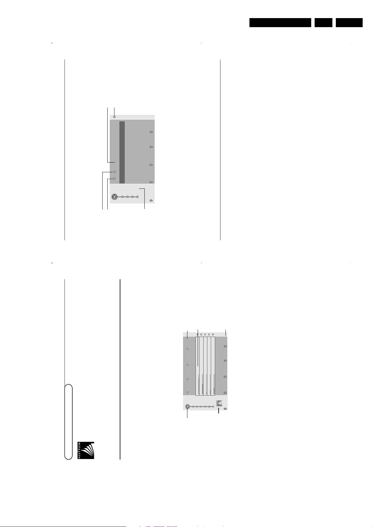
1.2 Connections
TOP CONTROLS
IR
Light sensor
Red
iTV only
LRSTB
Audio S-VideoCVBS-
Video
LR
No function
Centre In
L
R
PC Input (VGA)
Audio Out
Audio In
Figure 1-1 Side I/O and rear connections
1.2.1 Side I/O (Left Bottom Side)
Hosiden: SVHS (Input)
1 - Y Ground H
2 - C Ground H
3 - Y 1 V_pp / 75 ohm j
4 - C 0.3 V_pp / 75 ohm j
Cinch (Input)
- CVBS 1 V_pp / 75 ohm jq
- Audio - L 0.5 V_rms / 10 kohm jq
- Audio - R 0.5 V_rms / 10 kohm jq
Headphone (Output) (only for consumer TV sets)
- Headphone 32 - 600 ohm / 10 mW ot
Volume Program
Y
Pb
L
R
Pr
P/CHMENU/OK
ANT
ServiceEXT. 1/2/3/4 Mains
CL 36532053_066.eps
291003
STB (only for ITV)
- RJ-11 Only for ICONN jk
1.2.2 Audio receiver (if present)
Audio - In (Cinch)
C - Audio - Centre jq
Audio - Out (Cinch)
R - Audio - R 0.5 V_rms / 1 kohm kq
L - Audio - L 0.5 V_rms / 1 kohm kq
Audio - Out (Cinch)
R - Audio - R 0.5 V_rms / 1 kohm kq
L - Audio - L 0.5 V_rms / 1 kohm kq
Page 3
Technical Specifications, Connections, and Chassis Overview
EN 3FTL13E AA & AB 1.
1.2.3 VGA
VGA (Input)
1
6
11
5
10
15
Figure 1-2 VGA Connector
1 - Red 0.7 V_pp / 75 ohm j
2 - Green 0.7 V_pp / 75 ohm j
3 - Blue 0.7 V_pp / 75 ohm j
4 - Ground H
5 - Ground H
6 - Ground H
7 - Ground H
8 - Ground H
9 - 5V_DC_OUT +5 V_dc k
10 - Ground H
11 - Ground H
12 - DDC_SDA j
13 - H-sync 0 - 5 V j
14 - V-sync 0 - 5 V j
15 - DDC_SCL j
Cinch (Input)
- Audio - L 0.5 V_rms / 10 kohm jq
- Audio - R 0.5 V_rms / 10 kohm jq
- Y 0.7 V_pp / 75 ohm jq
- Pb 0.7 V_pp / 75 ohm jq
- Pr 0.7 V_pp / 75 ohm jq
1.2.4 SCARTs
121
202
CL96532137_056.eps
Figure 1-3 SCART connector
External 1: RGB/YUV and CVBS - In/Out
1 - Audio - R 0.5 V_rms / 1 kohm k
2 - Audio - R 0.5 V_rms / 10 kohm j
3 - Audio - L 0.5 V_rms / 1 kohm k
4 - Audio Ground H
5 - Audio Ground H
6 - Audio - L 0.5 V_rms / 10 kohm j
7 - Blue / U 0.7 V_pp / 75 ohm j
8 - CVBS-status 0 - 1.3 V: INT
4.5 - 7 V: EXT 16:9
9.5 - 12 V: EXT 4:3 j
9 - Video Ground H
10 - N.C.
11 - Green / Y 0.7 V_pp / 75 ohm j
12 - N.C.
13 - Video Ground H
14 - Video Ground H
15 - Red / V 0.7 V_pp / 75 ohm j
16 - Status / FBL 0 - 0.4 V: INT
1 - 3 V: EXT / 75 ohm j
17 - Video Ground H
18 - Video Ground H
19 - CVBS-out 1 V_pp / 75 ohm k
20 - CVBS-in 1 V_pp / 75 ohm j
21 - Shielding Ground H
171199
External 2: CVBS and SVHS - In/Out (for Recorder)
1 - Audio - R 0.5 V_rms / 1 kohm k
2 - Audio - R 0.5 V_rms / 10 kohm j
3 - Audio - L 0.5 V_rms / 1 kohm k
4 - Audio Ground H
5 - Audio Ground H
6 - Audio - L 0.5 V_rms / 10 kohm j
7 - C-out 0.7 V_pp / 75 ohm k
8 - CVBS-status 0 - 1.3 V: INT
4.5 - 7 V: EXT 16:9
9.5 - 12 V: EXT 4:3 j
9 - Video Ground H
10 - Easylink (P50) jk
11 - Green 0.7 V_pp / 75 ohm j
12 - N.C.
13 - Video Ground H
14 - Video Ground H
15 - C-in 0.7 V_pp / 75 ohm j
16 - Status / FBL 0 - 0.4 V: INT
1 - 3 V: EXT / 75 ohm j
17 - Video Ground H
18 - Video Ground H
19 - CVBS-out 1 V_pp / 75 ohm k
20 - CVBS-in 1 V_pp / 75 ohm j
21 - Shielding Ground H
External 3: CVBS - In
1 - Ground k
2 - Audio - R 0.5 V_rms / 10 kohm j
3 - Ground k
4 - Audio Ground H
5 - Ground H
6 - Audio - L 0.5 V_rms / 10 kohm j
7 - N.C.
8 - CVBS-status 0 - 1.3 V: INT
4.5 - 7 V: EXT 16:9
9.5 - 12 V: EXT 4:3 j
9 - Video Ground H
10 - N.C.
11 - N.C.
12 - N.C.
13 - Video Ground H
14 - Video Ground H
15 - N.C.
16 - N.C.
17 - Video Ground H
18 - Video Ground H
19 - N.C.
20 - CVBS-in 1 V_pp / 75 ohm j
21 - Shielding Ground H
Page 4
EN 4 FTL13E AA & AB1.
Technical Specifications, Connections, and Chassis Overview
External 4: CVBS - In
1 - Ground k
2 - Audio - R 0.5 V_rms / 10 kohm j
3 - Ground k
4 - Audio Ground H
5 - Ground H
6 - Audio - L 0.5 V_rms / 10 kohm j
7 - N.C.
8 - CVBS-status 0 - 1.3 V: INT
9 - Video Ground H
10 - N.C.
11 - N.C.
4.5 - 7 V: EXT 16:9
9.5 - 12 V: EXT 4:3 j
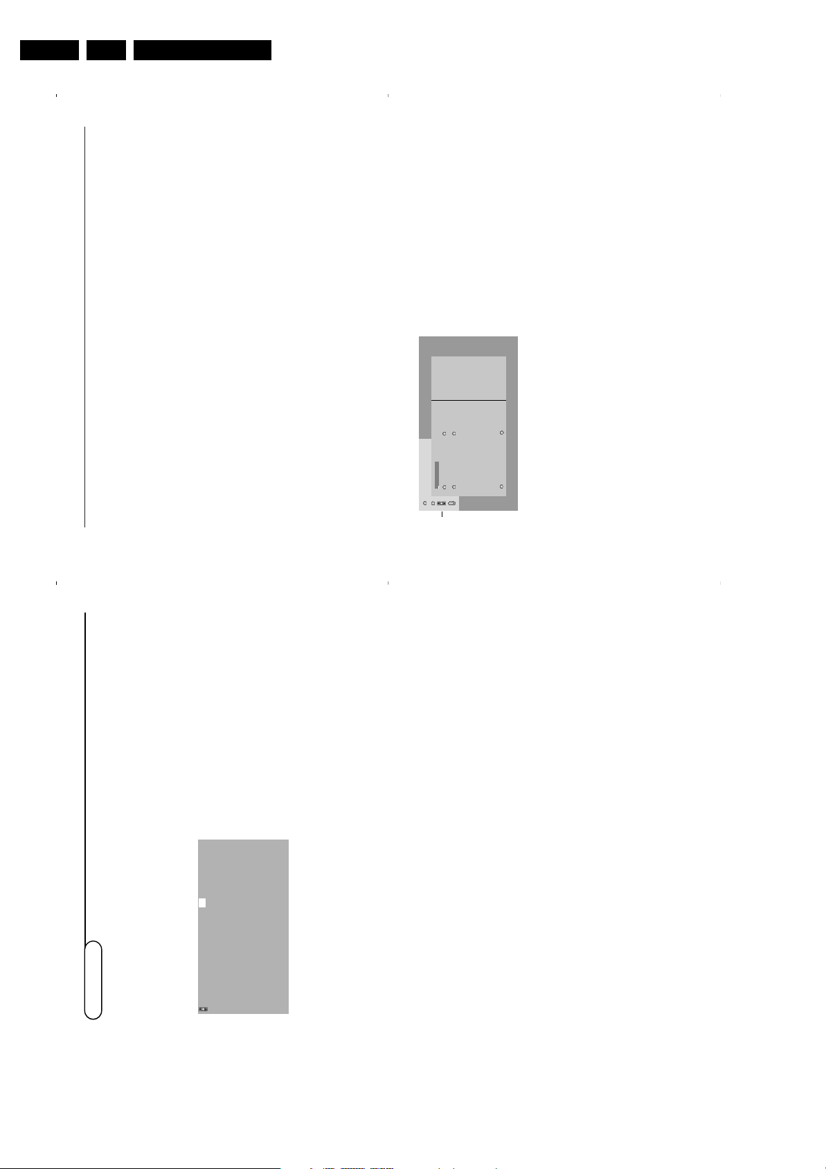
1.3 Chassis Overview
LED / MAINS SWITCH PANEL
LD
AUDIO AMPLIFIER
A
12 - N.C.
13 - Video Ground H
14 - Video Ground H
15 - N.C.
16 - N.C.
17 - Video Ground H
18 - Video Ground H
19 - N.C.
20 - CVBS-in 1 V_pp / 75 ohm j
21 - Shielding Ground H
Aerial - In
- IEC-type Coax, 75 ohm D
TOP CONTROL PANEL
AUX SUPPLY
P
SA
P
SIDE I/O PANEL
O
Figure 1-4 PWB location
POWER SUPPLY
SMALL SIGNAL PANEL
CL 36532053_054.eps
SP
B
090703
Page 5

Safety Instructions, Warnings, and Notes
2. Safety Instructions, Warnings, and Notes
EN 5FTL13E AA & AB 2.
Index of this chapter:
2.1 Safety Instructions
2.2 Warnings
2.3 Notes
2.1 Safety Instructions
Safety regulations require that during a repair:
• Connect the set to the Mains (AC Power) via an isolation
transformer (> 800 VA).
• Replace safety components, indicated by the symbol h,
only by components identical to the original ones. Any
other component substitution (other than original type) may
increase risk of fire or electrical shock hazard.
Safety regulations require that after a repair, the set must be
returned in its original condition. Pay in particular attention to
the following points:
• Route the wire trees correctly and fix them with the
mounted cable clamps.
• Check the insulation of the Mains (AC Power) lead for
external damage.
• Check the strain relief of the Mains (AC Power) cord for
proper function.
• Check the electrical DC resistance between the Mains (AC
Power) plug and the secondary side (only for sets which
have a Mains (AC Power) isolated power supply):
1. Unplug the Mains (AC Power) cord and connect a wire
between the two pins of the Mains (AC Power) plug.
2. Set the Mains (AC Power) switch to the "on" position
(keep the Mains (AC Power) cord unplugged!).
3. Measure the resistance value between the pins of the
Mains (AC Power) plug and the metal shielding of the
tuner or the aerial connection on the set. The reading
should be between 4.5 Mohm and 12 Mohm.
4. Switch "off" the set, and remove the wire between the
two pins of the Mains (AC Power) plug.
• Check the cabinet for defects, to avoid touching of any
inner parts by the customer.
2.2 Warnings
• All ICs and many other semiconductors are susceptible to
electrostatic discharges (ESD w). Careless handling
during repair can reduce life drastically. Make sure that,
during repair, you are connected with the same potential as
the mass of the set by a wristband with resistance. Keep
components and tools also at this same potential. Available
ESD protection equipment:
– Complete kit ESD3 (small tablemat, wristband,
connection box, extension cable and earth cable) 4822
310 10671.
– Wristband tester 4822 344 13999.
• Be careful during measurements in the high voltage
section.
• Never replace modules or other components while the unit
is switched "on".
• When you align the set, use plastic rather than metal tools.
This will prevent any short circuits and the danger of a
circuit becoming unstable.
2.3 Notes
2.3.1 General
• Measure the voltages and waveforms with regard to the
chassis (= tuner) ground (H), or hot ground (I), depending
on the tested area of circuitry. The voltages and waveforms
shown in the diagrams are indicative. Measure them in the
Service Default Mode (see chapter 5) with a colour bar
signal and stereo sound (L: 3 kHz, R: 1 kHz unless stated
otherwise) and picture carrier at 475.25 MHz for PAL, or
61.25 MHz for NTSC (channel 3).
• Where necessary, measure the waveforms and voltages
with (D) and without (E) aerial signal. Measure the
voltages in the power supply section both in normal
operation (G) and in stand-by (F). These values are
indicated by means of the appropriate symbols.
• The semiconductors indicated in the circuit diagram and in
the parts lists, are interchangeable per position with the
semiconductors in the unit, irrespective of the type
indication on these semiconductors.
• Manufactured under license from Dolby Laboratories.
“Dolby”, “Pro Logic” and the “double-D symbol”, are
trademarks of Dolby Laboratories.
2.3.2 Schematic Notes
• All resistor values are in ohms and the value multiplier is
often used to indicate the decimal point location (e.g. 2K2
indicates 2.2 kohm).
• Resistor values with no multiplier may be indicated with
either an "E" or an "R" (e.g. 220E or 220R indicates 220
ohm).
• All capacitor values are given in micro-farads (µ= x10
nano-farads (n= x10
• Capacitor values may also use the value multiplier as the
decimal point indication (e.g. 2p2 indicates 2.2 pF).
• An "asterisk" (*) indicates component usage varies. Refer
to the diversity tables for the correct values.
• The correct component values are listed in the Spare Parts
List. Therefore, always check this list when there is any
doubt.
2.3.3 Rework on BGA (Ball Grid Array) ICs
General
Although (LF)BGA assembly yields are very high, there may
still be a requirement for component rework. By rework, we
mean the process of removing the component from the PWB
and replacing it with a new component. If an (LF)BGA is
removed from a PWB, the solder balls of the component are
deformed drastically so the removed (LF)BGA has to be
discarded.
Device Removal
As is the case with any component that, it is essential when
removing an (LF)BGA, the board, tracks, solder lands, or
surrounding components are not damaged. To remove an
(LF)BGA, the board must be uniformly heated to a temperature
close to the reflow soldering temperature. A uniform
temperature reduces the chance of warping the PWB.
To do this, we recommend that the board is heated until it is
certain that all the joints are molten. Then carefully pull the
component off the board with a vacuum nozzle. For the
appropriate temperature profiles, see the IC data sheet.
Area Preparation
When the component has been removed, the vacant IC area
must be cleaned before replacing the (LF)BGA.
Removing an IC often leaves varying amounts of solder on the
mounting lands. This excessive solder can be removed with
either a solder sucker or solder wick. The remaining flux can be
removed with a brush and cleaning agent.
After the board is properly cleaned and inspected, apply flux on
the solder lands and on the connection balls of the (LF)BGA.
Note: Do not apply solder paste, as this has shown to result in
problems during re-soldering.
-9
), or pico-farads (p= x10
-12
-6
),
).
Page 6

EN 6 FTL13E AA & AB3.
Directions for Use
Device Replacement
The last step in the repair process is to solder the new
component on the board. Ideally, the (LF)BGA should be
aligned under a microscope or magnifying glass. If this is not
possible, try to align the (LF)BGA with any board markers.
To reflow the solder, apply a temperature profile according to
the IC data sheet. So as not to damage neighbouring
components, it may be necessary to reduce some
temperatures and times.
More Information
For more information on how to handle BGA devices, visit this
URL: www.atyourservice.ce.philips.com (needs subscription,
not available for all regions). After login, select “Magazine”,
then go to “Workshop Information”. Here you will find
Information on how to deal with BGA-ICs.
2.3.4 Lead Free Solder
Philips CE is going to produce lead-free sets (PBF) from
1.1.2005 onwards.
P
b
Figure 2-1 Lead-free logo
This sign normally has a diameter of 6 mm, but if there is less
space on a board also 3 mm is possible.
Regardless of this logo (is not always present), one must treat
all sets from this date onwards according to the following rules.
Due to lead-free technology some rules have to be respected
by the workshop during a repair:
• Use only lead-free soldering tin Philips SAC305 with order
code 0622 149 00106. If lead-free solder paste is required,
please contact the manufacturer of your soldering
equipment. In general, use of solder paste within
workshops should be avoided because paste is not easy to
store and to handle.
• Use only adequate solder tools applicable for lead-free
soldering tin. The solder tool must be able
– To reach at least a solder-tip temperature of 400°C.
– To stabilise the adjusted temperature at the solder-tip.
– To exchange solder-tips for different applications.
• Adjust your solder tool so that a temperature around 360°C
- 380°C is reached and stabilised at the solder joint.
Heating time of the solder-joint should not exceed ~ 4 sec.
Avoid temperatures above 400°C, otherwise wear-out of
tips will rise drastically and flux-fluid will be destroyed. To
avoid wear-out of tips, switch “off” unused equipment or
reduce heat.
• Mix of lead-free soldering tin/parts with leaded soldering
tin/parts is possible but PHILIPS recommends strongly to
avoid mixed regimes. If not to avoid, clean carefully the
solder-joint from old tin and re-solder with new tin.
• Use only original spare-parts listed in the Service-Manuals.
Not listed standard material (commodities) has to be
purchased at external companies.
• Special information for lead-free BGA ICs: these ICs will be
delivered in so-called "dry-packaging" to protect the IC
against moisture. This packaging may only be opened
short before it is used (soldered). Otherwise the body of the
IC gets "wet" inside and during the heating time the
structure of the IC will be destroyed due to high (steam)pressure inside the body. If the packaging was opened
before usage, the IC has to be heated up for some hours
(around 90°C) for drying (think of ESD-protection!).
Do not re-use BGAs at all!
• For sets produced before 1.1.2005, containing leaded
soldering tin and components, all needed spare parts will
be available till the end of the service period. For the repair
of such sets nothing changes.
In case of doubt whether the board is lead-free or not (or with
mixed technologies), you can use the following method:
• Always use the highest temperature to solder, when using
SAC305 (see also instructions below).
• De-solder thoroughly (clean solder joints to avoid mix of
two alloys).
Caution: For BGA-ICs, you must use the correct temperatureprofile, which is coupled to the 12NC. For an overview of these
profiles, visit the website www.atyourservice.ce.philips.com
(needs subscription, but is not available for all regions)
You will find this and more technical information within the
"Magazine", chapter "Workshop information".
For additional questions please contact your local repair help
desk.
2.3.5 Practical Service Precautions
• It makes sense to avoid exposure to electrical shock.
While some sources are expected to have a possible
dangerous impact, others of quite high potential are of
limited current and are sometimes held in less regard.
• Always respect voltages. While some may not be
dangerous in themselves, they can cause unexpected
reactions that are best avoided. Before reaching into a
powered TV set, it is best to test the high voltage insulation.
It is easy to do, and is a good service precaution.
3. Directions for Use
You can download this information from the following websites:
http://www.philips.com/support
http://www.p4c.philips.com
Page 7
Directions for Use
2
Preparation
&
Wall mounting instructions
For the wall mounting instructions follow the
illustrated steps xx to xx printed on the
separate template.
Make sure that the wall mount is being fixed
securely enough so that it meets safety
standards.The weight of the TV (excl.
packaging) is about 17 kg.
How to mount the supplied stand, see the
separate leaflet.
Note: other (not supplied) stands are optional
accessories. Consult your dealer.éPlace or hang the TV wherever you want,but
make sure that air can circulate freely through
the ventilation slots. Do not install the TV in a
confined space such as a book case or a
simular unit.
To prevent any unsafe situations, no naked
flame sources, such as lighted candles, should
be placed on or in the vicinity.Avoid heat,
direct sunlight and exposure to rain or water.
The equipment shall not be exposed to
dripping or splashing and no objects filled with
liquids, such as vases,shall be placed on it.
“
Insert the aerial plug firmly into the aerial
socket x at the bottom of the TV. For best
picture quality use the suppressor-aerial cable
supplied.‘To connect your computer, see p. 20.
To connect other peripherals, see p. 17.
If you dispose of a Cinema Link combination
(Cinema Link Audio receiver and/or Cinema
Link video recorder and/or DVD player), see
the separate supplied instruction manual.
In order to obtain the best result, please use
only the supplied antenna cables between the
TV and videorecorder, and between
videorecorder and antenna connector.(Insert the mains cord supplied into the mains
at the bottom of the TV and in the wall socket
having a mains voltage of 220-240V.
To prevent damaging the power (AC) cord
which could cause a fire or electric shock, do
not place the TV on the cord.
§
Remote control
: Insert the 2 batteries
supplied (Type R6-1,5V).
The batteries supplied do
not contain the heavy
metals mercury and
cadmium. Please check on
how to dispose of
exhausted batteries
according to local regulations.
è
Switch the TV on
: Press the power switch B
at the right side of the TV.
An indicator on the front of the TV lights up
and the screen comes on. If the TV is in
standby mode, press the
-P+
keys or the B
key on the remote control.
1m
min.
Keys on top of the TV
Should your remote be lost or broken you can still
change some of the basic settings with the keys on top
of your TV.
Press:
• the V
-
or
+
key to adjust the volume;
• the
-P/CH+
keys to select the TV channels or sources.
The
MENU/OK
key can be used to summon the main
menu without the remote control.
Use:
• the V - and + keys and the
P/CH-
and
P/CH+
keys
to select menu items in the directions as shown;
• the
MENU/OK
key to confirm your selection.
Note:
When activated via the
MENU/OK
key on top of the TV,
only
Exit
lets you dismiss the menu.
Navigate to
Exit
and press the
MENU/OK
key.
MENU/OK - V + - P/CH +
TV
Setup
Install
Exit
Picture Sound Features
1
Contents
Preparation ...................................................................................... 2
Keys on top of the TV ................................................................... 2
Your remote control .................................................................. 3-4
To use the menus ........................................................................... 5
Select the menu language and country ..................................... 5
Store TV channels .......................................................................... 6
Automatic installation ............................................................6
Manual installation................................................................... 6
Give name ................................................................................. 7
Reshuffle the programme list................................................. 7
Select favourite TV channels ................................................. 7
TV setup menu ............................................................................... 7
General ...................................................................................... 8
Source ........................................................................................ 9
Decoder .................................................................................... 9
Demo ............................................................................................... 9
Installation
TV menu
Picture menu .................................................................... 10-11
Sound menu ........................................................................... 11
Features menu ................................................................. 11-12
NEX
TV
IEW
/Teletext guide ...................................................... 13-14
Teletext ..................................................................................... 15-16
Connect peripheral equipment
Connecting and selecting equipment ............................... 17-20
Audio and Video equipment keys ............................................. 21
Record with your recorder with Easy Link ........................... 21
Tips ................................................................................................ 22
Operation
EasyLink features are based on the “one touch operation” approach.This
means that a sequence of actions are executed at the same time in both the
television and the video cassette recorder, provided both are fitted with the
EasyLink function and connected with the eurocable supplied with your video
recorder.
R
End of life directives
Philips is paying a lot of attention to
producing environmentally-friendly in
green focal areas.Your new TV contains
materials which can be recycled and
reused. At the end of its life specialised
companies can dismantle the
discarded TV to concentrate the
reusable materials and to minimise
the amount of materials to be
disposed of.
Please ensure you dispose of your old
TV according to local regulations.
Help?
If this instruction manual does
not give an answer or if ‘Tips’ do
not solve your TV problem, you
can call your Local Philips
Customer or Service Centre. See
the supplied World-wide
guarantee booklet.
Please, have the Model and
Product number which you can
find at the back of your
television set or on the
packaging, ready, before calling
the Philips helpline.
Model: 30PF9975
Product No: ...........................................
Care of the screen
See Tips, p. 22.
EnglishDeutschFrançaisNederlandsItaliano
∂ППЛУИО¿
EN 7FTL13E AA & AB 3.
Page 8
EN 8 FTL13E AA & AB3.
4
i On Screen information
Press to display (when available) information about the selected TV
channel and programme.
Menu/Remote control info
When a menu is on screen, press
i
to display info on the selected menu
item.While the menu info is displayed, press any key to display remote
control info.The normal function of the key is not executed.
b
no function
h Active control
see p. 11.
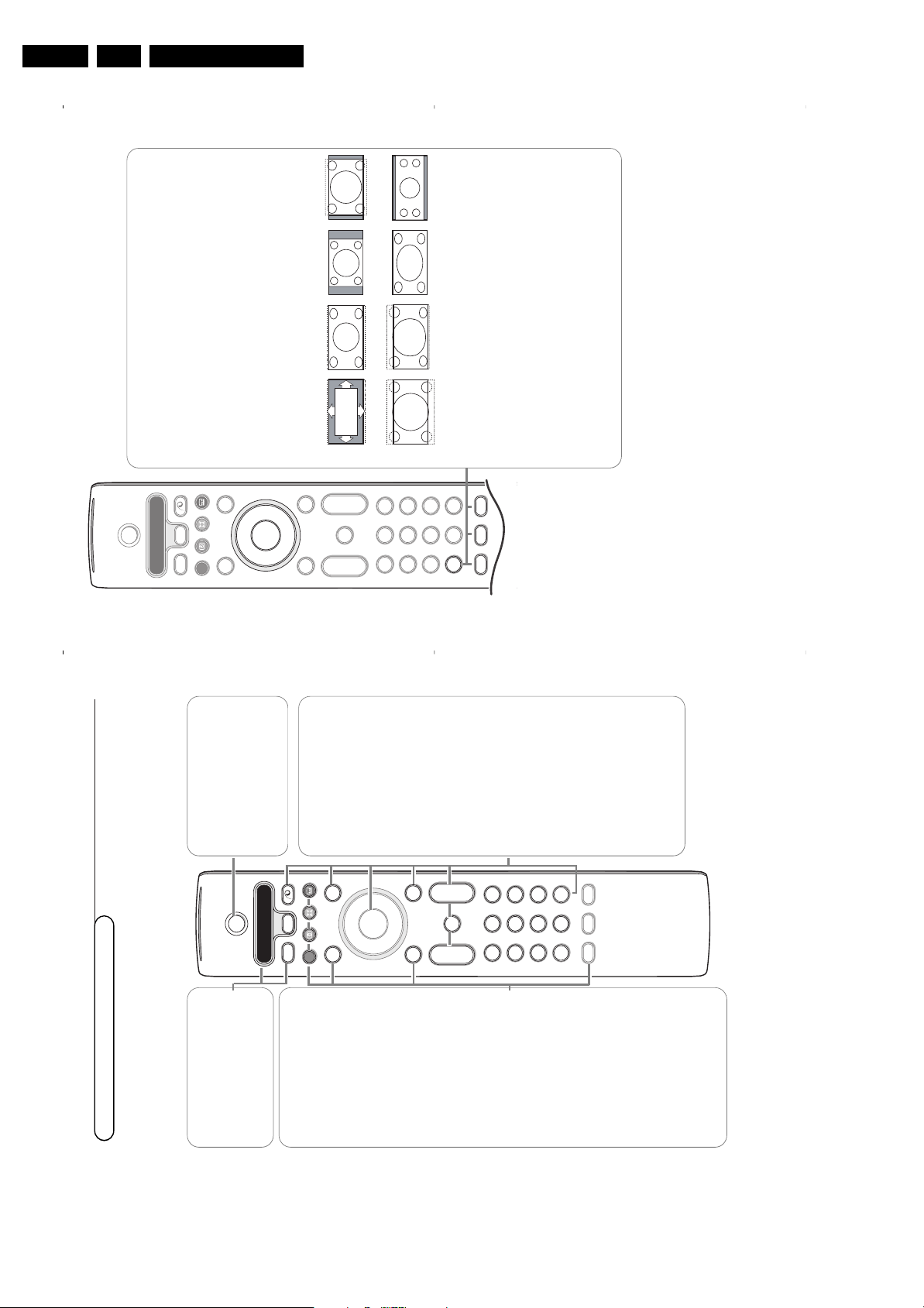
q Picture format
Press this key repeatedly or press the cursor up/down to select another
picture format:Auto format, Super zoom, 4:3, Movie Expand 14:9, Movie
Expand 16:9, Subtitle zoom,Wide screen or 16:9.
Auto format makes the picture fill the screen as much as possible.
In case of subtitles in the bottom black bar,Auto format makes the
subtitles visible.
In case of a broadcaster logo in the corner of the top black bar, the logo
disappears from the screen.
Super zoom removes the black bars on the sides of 4:3 programs with
minimal distortion.
When in Movie Expand 14:9, Movie Expand 16:9, Super zoom or Subtitle
zoom picture format, you can make subtitles visible with the cursor
up/down.
Note: With signals via
EXT5
or the
VGA IN
connector less picture formats are
selectable.
Auto format Super zoom 4:3 Movie Expand 14:9
Movie Expand 16:9 Subtitle zoom Wide screen 16:9
B
b
¬
+
-
V
+
-
P
v
b
i
0
h
q
Select
VCR DVD SAT AMP CD
MENU
OK
123
456
789
0
Ò
®
‡π
†
Active Control
S
®
®
®
®
æ
3
Use of the remote control RC4301
3
B Standby
Press to switch the TV on or off.
When switched off, a red indicator on
the TV lights up.When acquiring
NEX
TV
IEW
, see p. 14, an orange
indicator lights up and after a period
of max. 1 hour the TV is switched to
full standby and the red indicator
lights up.
®Ò‡π†
Audio and Video equipment keys,
see p. 21.
® Instant record
See Record with your recorder
with EasyLink, p. 21.
U Time display
The time is displayed on the
screen.
Q Surround mode
Incredible surround
With stereo transmission, and
when Incredible surround is
selected, it seems as though the
loudspeakers are spread further
apart from one another.
Virtual Dolby surround
Optimal with Dolby surround
signals. Enables you to
experience the effect of Dolby
surround Pro Logic, reproducing
a rear sound effect. See Sound
menu, 3D effect, p. 11.
Note:You can make the same
selection in the Sound menu,
surround mode, p. 11.
Ì Cinema Go
See separate Cinema Link
booklet supplied.
æ
NEX
TV
IEW
On/Off see p. 13
S Freeze
To freeze the picture.
Dependent on the input signal,
the function may not be possible.
VCR DVD SAT AMP CD
See ‘Audio- and Video equipment
keys’, p. 21.
v Select your computer or
other peripherals
See p. 18.
x Pixel Plus demo
on/off
In the right part Pixel Plus and
Digital Natural Motion are
switched on.
b Teletext
On/Off see p. 15
OK
Press this key
• to activate your choice, when in
the menus.
• to display the programme list.
MENU
Main menu
on/off see p. 5
V
To adjust the volume.¬Interrupt the sound or restore it.
P Programme selection
To browse through the TV
channels and sources stored in
the favourite list.
0/9 Digit keys
To select a TV channel.
For a two digit programme
number,enter the second digit
before the dash disappears.To
switch immediately to a selected
one digit TV channel, keep the
digit key pressed a bit longer.
0 Previous TV channel
Press to display the previously
selected TV channel.
Note: For most keys pressing a key once will activate the function. Pressing a second time will de-activate it.
When a key enables multiple options, a small list will be shown. Press repeatedly to select the next item in the list.
The list will be removed automatically after 4 seconds or press
OK
to remove immediately.
Remark: in VGA mode only some keys are valid.
B
b
¬
+
-
V
+
-
P
v
b
i
0
h
q
Select
VCR DVD SAT AMP CD
MENU
OK
123
456
789
0
Ò
®
‡π
†
Active Control
S
®
®
®
®
æ
Directions for Use
Page 9
Directions for Use
6
&
Select
Automatic install
in the Install menu.
Note: All channels must be unlocked in order to autoprogram. If
requested, enter your code to unlock all channels. (See TV,
Features menu, Childlock, p. 12.)
é
Press the cursor down.
The autoprogramming option label
Start
appears.
“
Press the cursor right.
‘
The message
Searching
appears and the progress of
autoprogramming is displayed.
If a cable system or a TV channel which broadcasts ACI
(Automatic Channel Installation) is detected, a programme list
appears.Without ACI broadcast,the channels are numbered
according your language and country selection.You can use
Reshuffle to renumber them. See p. 7.
It is possible that the cable company or the TV channel displays a
broadcast selection menu. Layout and items are defined by the cable
company or the TV channel. Make your choice with the cursor and
press the
OK
key.
After language and country are set correctly, you can now search for and store the TV channels in two
different ways: using Automatic Installation or Manual Installation (tuning-in channel by channel).
Select your choice with the cursor right.
Automatic install
Install Start
Install
Manual installation
Automatic installation
Searching for and storing TV channels is done channel by
channel.You must go through every step of the Manual
Installation menu.
&
Select
Manual install
in the Install menu.
é
Press the cursor down.
Follow the instructions on screen.
Note: Search or direct selection of a TV channel.
If you know the frequency, the C- or S-channel number, enter the
3 or 2 digits of the frequency or the channel number directly with
the digit keys 0 to 9 (e.g. 048). Press the cursor down to proceed.
Repeat to search for another TV channel.
Manual install
Install
Selection mode
System
Programme
Search
Fine tune
Store
Store TV channels
5
To use the menus
&
Press the
MENU
key on the remote control to summon the
main menu.At any moment you can exit the menu by
pressing the
MENU
key again.
Note: If you have connected equipment with Cinema Link, more
menu items are present.
é
Use the cursor in the up/down direction to select the
TV
,
Setup, Demo
or
Install
menu.
Use the cursor left/right to select
Picture
,
Sound
or
Features
.
Note: Sometimes not all the menu items are visible on the screen
(indicated by a cluster of blue balls). Use the cursor down or right
to reveal all items.
“
Use the cursor in the left/right direction to select the menu
item.‘Use the cursor up/down again to select the control you
want to select or to adjust.
Note: Items temporary not available or not relevant are displayed in a
light grey colour and cannot be selected.
B
b
¬
+
-
V
+
-
P
v
Select
VCR DVD SAT AMP CD
MENU
OK
Ò
®
‡π
†
S
®
®
®
®
æ
cursor to select
adjustments
OK
key to
activate
return or switch
main menu on/off
Installation
&
Press the
MENU
key on the remote control.
é
Use the cursor down to select
Install
.
“
Use the cursor right to select
Language
.
Follow the instructions on screen.
‘
Use the cursor up/down to select your preferred language
and press the
OK
key to confirm your selection.
(
Use the cursor right to select
Country
.
§
Select the country where you are now located and press
the
OK
key.
Select
Other
when none of the countries applies.
è
Proceed with the
Install
menu.
TV
Setup
Demo
Install
Picture Sound Features
Install
Language Country Automatic Manual Give name Reshuffle Favourite
install install programmes
The installation menu contains the following items:
EasyLink
If your video recorder has an EasyLink function, during installation, the language, country and available channels are
automatically transmitted to the video recorder.
Language
English
Deutsch
Français
Install
Country
Austria
Belgium
Croatia
Install
Select the menu language and country
EN 9FTL13E AA & AB 3.
Page 10
EN 10 FTL13E AA & AB3.
8
General
Menu background
Select
Ye s
or
No
to turn the menu background
on or off.
Factory settings
This resets the picture and sound settings to
their predefined factory values, but maintains
the channel installation settings.
NEX
TV
IEW
provider
Select a TV broadcaster that provides
NEX
TV
IEW
data. How to make use of
NEX
TV
IEW
,
see p. 13.
OSD (On Screen Display)
&
Select
OSD
.
é
Select
Normal
to activate extended channel
and programme information.
Minimum
will
display reduced channel information.
Note: When subtitles is switched on, see Features,
p.12, display of the programme number is not
possible
Programme title
Select
Programme title Yes
or
No
.
When selected
Ye s
, after the selection of a TV
programme or after pressing the i key on
the remote control, a TV channel which
broadcasts teletext may transmit the name of
the TV channel or the programme title.
When selected
No
, the programme title will
only appear after pressing the i key, and not
after the selection of a TV channel.
Teletext level 2.5
Some broadcasters offer the opportunity to
see more colours, other background colours
and nicer pictures in the teletext pages.
&
Select
Teletext level 2.5
.
é
Press the cursor right to select
Teletext level
2.5 On
to take advantage of this feature.
“
Press the cursor right again to select
Teletext
level 2.5 Off
if you like the more neutral
teletext layout.
The selection made is valid for all channels
which broadcast teletext level 2.5.
Note: It may take a few seconds before teletext
broadcast switches over to Teletext level 2.5.
Auto Surround
Sometimes the broadcaster transmits special
signals for Surround Sound encoded
programmes.
The TV automatically switches to the best
surround sound mode when
Auto Surround
is
switched
On
.
Set/Change code
The Child lock feature (see TV, Features, p. 12)
allows you to lock channels to prevent others
from watching certain programmes.To watch
locked channels, a 4-digit code must be
entered.The Set/Change code menu item
allows you to create or change a Personal
Identification Number (PIN).
&
Select
Set/Change code
.
é
If no code exists yet, the menu item is set to
Set code
.
If a code has previously been entered, the menu
item is set to
Change code
. Follow the
instructions on screen.
Important:You have forgotten your code !
&
Select
Change code
in the General menu and
press
OK
.
é
Press the cursor right and enter the overriding
code 8-8-8-8.
“
Press the cursor again and enter a new
personal 4-digit code.The previous code is
erased and the new code is stored.
This menu allows you to change various settings that are presumably adjusted less frequently than most
other settings.
Press the
i
key on the remote control to get information about the selected menu item.
It is possible to change the name stored in the
memory or to assign a name to a TV channel or
external for which a name has not yet been
entered.A name with up to 5 letters or numbers
can be given to the programme numbers 0 to 99.
Note : It is not possible to rename the VGA source.
&
Select
Give Name
in the Install menu and
press the cursor down.
é
Select the programme number.
Note: keep the cursor up/down pressed to scroll
through the programme list quickly.“Press the cursor right.
A keyboard appears on the screen.
Press the cursor right to enter the keyboard.
Press the cursor up/down, left/right to select
the first character and press
OK
. Repeat for
every character you want to enter.
Select
Space
to enter a space;
Delete
to erase
the highlighted character in the name entered;
Shift
to display upper- or lowercase characters
on the keyboard;
Special
to display special
characters on the keyboard. Press
OK
to
confirm.
‘
Press the cursor left repeatedly when you have
finished the name giving.
(
Select another programme number and repeat
steps
“
to
‘
.
7
Give name
pπ
® Space ® Delete
ABCDEFG 123
HIJKLMN 456
OPQRSTU 789
VWXYZ 0
® Shift ® Special
Give name
Install
VCR1
BBC1
BBC2
CNN
TVE
.....
Reshuffle the programme list
You can change the order of the stored TV
channels.
&
Select
Reshuffle
in the Installation menu.
é
Follow the instructions on screen.
Select Favourite TV channels
A VGA source always belongs to the list of
Favourite programmes
.
&
Select
Favourite programmes
in the Install
menu.
é
Select your programme number with the
cursor up/down.
“
Select
Ye s
or
No
with the cursor right.
‘
Repeat
é
and
“
for every TV channel or
external you want to make a favourite or a
non-favourite TV channel or external.
TV Setup
The Setup menu contains items that control the settings
of the TV’s functions,features, services and peripherals
you may have connected.
The
General
menu allows you to change settings that
will typically be accessed only occasionally.
The
Source
menu allows you to select a source.
The
Decoder
menu allows you to define one or more
programme numbers as decoder programme numbers.
General
Menu background
Factory settings
NEX
TV
IEW
provider
OSD
Programme title
Teletext level 2.5
Auto surround
Set/Change code
Setup
Directions for Use
Page 11
Directions for Use
&
Press the cursor right to select
Picture
.
é
Select the menu items in the Picture menu with the cursor
up/down.“Adjust the settings with the cursor left/right or enter the list of
submenu items with the cursor right. Select a submenu item
with the cursor up/down.
Note:To remove the menu background before adjusting the picture
settings, see Select TV setup, General, p. 8.
Smart picture
Select
Smart picture
to display a list of predefined picture
settings, each corresponding with specific factory settings.
Personal
refers to the personal preference settings of picture in
the picture menu.
Digital options
Pixel Plus is the most ideal setting, doubles the horizontal
resolution and increases the number of lines with 33%.
You may consider to select Movie Plus in case a halo effect
should disturb you. Dependent on your own preference, select
Progressive scan.
Dynamic contrast
Sets the level at which the TV automatically enhances the details
in dark, middle and light areas of the picture.
DNR
This sets the level at which noise is measured and reduced in
the picture.
Colour enhancement
This makes the colours more vivid and improves the resolution
of details in bright colours.
Hue
This compensates for the colour variations in NTSC encoded
transmissions.
Picture format
This will adjust the size of the picture dependent on the
broadcast format and your preferred setting.
TV menu
Press the
MENU
key on the remote control to summon the main menu.
Note: Dependent on the input signal, one or more menu items may not be selectable.
Press the i key on the remote control to get information about the selected menu item.
Picture Sound Features
Smart picture
Contrast
Brightness
Colour
Sharpness
Tint
Digital options
Dynamic contrast
DNR
Colour enhancement
(Hue)
Picture format
TV
10
Picture menu
9
Source
This menu allows you to indicate the peripheral
you connected to one of the external inputs.
&
Press the cursor right to enter the list of types
of peripherals attached to the selected input.
é
Select the peripheral device with the cursor
up/down.
Once you have selected the source type, e.g. DVD,
this source will automatically be selected when
your remote control is in DVD mode, see p. 3, and
when you press the v key on the remote
control.
Centre input - Centre in volume
When you have connected a surround receiver
to the TV, see p. 18, the loudspeakers of the TV
can act as centre speaker, making a separate
centre speaker unnecessary.
Select
Centre input On
or
Cinema Link
(in
case you have connected a Cinema Link
Surround receiver).
When having selected
On
you can adjust the
Centre in volume with the cursor left/right to
correct volume level differences of the external
audio receiver and speakers.
Note:This is not the case with a Cinema Link
surround receiver.
Source
EXT1
EXT2
EXT3
EXT4
YPbPr
FRONT
Centre input
Centre in volume
Setup
If a decoder or a descrambler is connected, see
p. 17, you can define one or more programme
numbers as decoder programme numbers.
&
Select
Decoder
with the cursor right.
é
Select
Programme
.
“
Select the programme number under which
you have stored the programme coming from
your decoder.‘Select
Status
.
• Select the input used to connect your
decoder:
None
,
EXT1
or
EXT2
.
• Select
None
if you do not want the selected
programme number being activated as a
decoder programme number.
Note: Select
EXT2
when the decoder is connected to
your EasyLink video recorder.
Decoder
Decoder
Programme
Status
Setup
Demo
The Demo menu allows to demonstrate the TV
features separately or in a continuous loop.
If
Auto demo
has been selected the demo will
automatically present the features sequentially in a
loop. Press one of the cursor keys to stop the Auto
demo.
If one of the features has been selected, this
particular feature demo will run only once, and the
Demo menu will reappear.
Note:The Dealer demo is not par t of the automatic
sequence and can only be activated separately.
Auto demo
......
Dealer demo - Digital options
- Light sensor
- Comb filter
TV
Setup
Demo
Install
EN 11FTL13E AA & AB 3.
Page 12

EN 12 FTL13E AA & AB3.
12
Programme list
Press the
OK
key to switch over to the
selected TV channel or external.
Select subtitles
The subtitle page must be stored for each TV
channel:
Switch on teletext and select the proper
subtitle page from the index. Switch off
teletext.
Subtitle On
will automatically display them on
the selected TV channels if subtitles are in the
transmission.A symbol will indicate that the
mode is on.
Select
On during mute
when you want to
have the subtitles automatically displayed only
when the sound has been muted with the ¬
key on the remote control.
Child lock
Note: A VGA source can not be locked.
&
Select
Child lock
.
é
Press the cursor right to enter the Child lock
menu.You’re summoned to enter your code.
Note:You have to re-enter your code each time you
enter the child lock menu.
Important:You have forgotten your code !
See p. 8.
“
Select one of the menu items of the child lock
menu:
•
Lock
if you want to lock all channels and
externals.
•
Custom lock
and press the cursor right.
Select:
-
Lock after
if you want to lock all programmes
from a certain time onwards.
Press the cursor right and enter the time with
the cursor up/down and right. Press the
OK
key to validate.
-
Programme lock
if you want to lock a certain
TV channel or external;
• Select
Unlock
to disable all locks you have set.
On timer
&
Select
On timer
with the cursor down.
é
Select
On
with the cursor right.
“
Press the cursor right again to enter the
programme list.
‘
Select the TV channel or external you want
your TV to switch to on a selected time and
day.(Press the cursor right again to select a day of
the week or to select
Daily
.
§
Press the cursor right once again to enter the
time with the digit keys or with the cursor
up/down and press the
OK
key to activate.
è
Press the
MENU
key to turn off the menu.
Note:To check your timer settings, press the i
key.
Zoom
Note: Dependent on the input signal, Zoom may not be
selectable.
&
Select
Zoom
with the cursor down and press
the ok key.
é
Press the
OK
key to select one of the zoom
magnifications (x1, x4,x9, x16).
“
Additionally you can shift the selected zoom
window over the screen with the cursor keys
up/down, left/right.‘Press the
MENU
key to turn off the zoom
function.
Child lock
Lock
Custom lock
Unlock
Lock after
Programme lock
VCR1
BBC2
CNN
TVE
π.....
Sunday
Monday
.......
Daily
15:45
On timer
Off
On
11
The TV continuously measures and corrects all
incoming signals in order to provide the best
picture possible.
&
Press the h key on the remote control.éThe Active Control menu appears.“Press the cursor up/down to select the Active
Control values
Off
,
Minimum
,
Medium
(recommended) or
Maximum
.
The picture settings are being optimised
continuously and automatically which is
displayed by bars.The menu items can not be
selected.
‘
Press the cursor right to select
Smart
Picture
.
(
Press the cursor up/down to select one of the
predefined picture settings.
§
Press the cursor right to select
Active
Display
.
è
Press the cursor up/down to select
Show bars
,
one of the Dual screen demos or
Off
.
When you select Dynamic contrast, Pixel Plus,
Digital Noise Reduction or Digital Natural
Motion, the TV screen is divided into two parts:
in the left part the selected picture quality
setting is switched off; in the right part it is
switched on.
Note: Dependent on the input signal, one or more
Dual screen demos may not be selectable.
!
Press the h key again to switch off the Active
Control menu.
Active Control
&
Press the cursor right to select
Sound
.
é
Select the menu items in the Sound menu with the cursor
up/down and adjust the settings with the cursor
left/right.Remember,control settings are at normal mid-range
levels when the bar scale is centred.
Smart sound
Select Smart sound to display a list of predefined sound settings,
each corresponding with specific factory settings of Treble and
Bass.
Personal
refers to the personal preference settings of
sound in the sound menu.
Notes:
- Some menu items are only available in case of a Cinema Link
configuration and when the Cinema Link is activated. Others are
steered by the audio receiver instead of by the TV. See the separate
Cinema Link booklet supplied.
- Dual X is only available with dual sound transmission.
- Mono/Stereo is only selectable in case of analogue stereo
transmission.
- Nicam/Analogue is only selectable in case of Nicam transmission.
Sound
Smart sound
Equalizer
Volume
Balance
Loudness
Headphone volume
Surround mode
(Dual I-II)
(Mono/Stereo)
(Nicam/Analogue)
(3D effect)
AVL
Delta volume
TV
Sound
OffOnOn during mute
Features
Programme list
Subtitle
Sleeptimer
Child lock
On timer
Zoom
TV
Features menu
&
Press the cursor right to select
Features
.
é
Select the menu items with the cursor
up/down and adjust the settings with the
cursor left/right.
Use the on-screen Menu-Info
i
for more
information about the menu items.
Directions for Use
Page 13
Directions for Use
1414
Teletext Guide
&
Enter with the digit keys, the teletext page number that contains the programme information for the
current channel.
é
Press the cursor right to move the puck over the selection ball.
“
Use the cursor up/down to scroll through the different programmes.
• If the selected programme contains a page number with an optional subcode referring to a page with
more info about the programme, press the
OK
key to display the information.Press the
OK
key again
to return to the programme guide page.
• If the selected programme guide page satisfies the VPT requirements,
- it will be possible to record, remind, watch or lock programmes:
- the TV will remember the last selected teletext page number of that channel that contains programme
guide information and indicates which programme starts at what time. Every time you press the æ
key, the teletext programme guide page of the selected TV channel will be available.
• When necessary you can select the subpage number by moving the cursor to the pageball and
pressing right.
Note:You must enter the teletext pagenumber for each channel.You can change the channels also by moving
the cursor up/down in the list in the left of the page.
Basic functions
Press one of the grey x,red ®, green U, yellow Q or blue Ì keys to activate a
NEX
TV
IEW
or
Teletext Guide function.The keys appear in grey if the function is not available.
Review
: this menu provides a list of programmes that are marked as reminders, those that have to be
recorded and those that are locked.This menu can be used to change or remove marked
programmes.
Record
: to programme the recording of the video recorder (if it has a
NEX
TV
IEW
Link function and is
connected to
EXT. 2
).
Remind
: automatically switch on the TV if it is in standby or by displaying a message if the TV is on.
Lock
: to lock certain programmes to prevent recording or watching.
For the functions Record, Remind or Lock, a small menu pops up in which you can choose the
interval: once, daily or weekly, or clear an earlier made record, remind or lock setting.The default
interval is set to
Once
.To confirm the frequency, press the
OK
key.
Watch
: to watch the selected and currently broadcast programme.
Acquisition and updating of
NEX
TV
IEW
information
Acquisition and updating of
NEX
TV
IEW
is done when you are watching the TV channel of the selected
NEX
TV
IEW
provider, see Setup menu, p. 8, or when the TV is switched to standby;
Acquisition of fresh data will happen once during the night.
Note: it may be necessary to put the TV in standby mode when all
NEX
TV
IEW
information is outdated, e.g. when
returning from holiday.
Review Record Remind Watch Lock
BBC1
BBC2
ITV
CH4
CH5
page ball
selection ball
channel list
Mon 05 Feb 16.35
100 1
BBC CEEFAX
LIONS RECORD ANOTHER WIN 430
Index 100 News 300
BBC Info 110 Headlines 305
Children 120 Weather 400
Cookery 150 Sports 415
Education 200 Radio 500
subpages
scroll ball
1313
NEX
TV
IEW
/ Teletext guide
NEX
TV
IEW
is an electronic guide that allows you to look up programmes as you would in a
newspaper or a TV magazine.You can sort the programmes by subject (films, sport...), obtain
detailed information and programme your video recorder if it comes with the
NEX
TV
IEW
Link
function.
Important note: The
NEX
TV
IEW
service is only available on certain programmes and in certain
countries. When no
NEX
TV
IEW
information is broadcast, the teletext programme guide appears in its place.This is
based on teletext programme information (if available) and offers most functions of
NEX
TV
IEW
.
Note:The broadcaster is responsible for the content of the information.
Call
NEX
TV
IEW
/ Teletext guide
Press the æ key on the remote control to call the
NEX
TV
IEW
/Teletext guide.A menu appears with
the message
One moment please
.After a while you obtain:
•a
NEX
TV
IEW
page, if the selected channel broadcasts this service (the
NEX
TV
IEW
logo is displayed),
• a teletext page, if the selected channel does not broadcast
NEX
TV
IEW
,
•
No information available
is displayed if neither
NEX
TV
IEW
nor teletext are transmitted. In this case,
select another channel.
Display of a
NEX
TV
IEW
page
The information is set by the channel that transmits the
NEX
TV
IEW
service. See also Setup menu,
General,
NEX
TV
IEW
provider, p. 8.
This logo is only displayed
during a
NEX
TV
IEW
transmission or when one
of the externals is selected.
No logo indicates a teletext
programme guide
Programme name and
broadcast time
Review Record Remind Watch Lock
Mon 03
Mon 03
Tue 04
Wed 05
Thu 06
Fri 07
Sat 08
puck
function keys
NEX
TV
IEW
guides
BBC1 18.00 BBC News
BBC2 18.00 The Simpsons
CNN 18.00 World News
FR2 18.00 On a tout essayé!
CH5 18.15 Tomorrow Never Dies
Menu 18.00 Channel Theme
Mon
05
Feb
18.00
NEX
TV
IEW
guides
&
Use the cursor key left/right to select
Time
,
Channel
,
Theme
, the
Date
guide.
The
Time guide
provides an overview of all programme titles active in the selected time block.The
Channel guide
provides an overview of all programmes that are broadcast by a single channel during
one day. With the
Date guide
you can choose a specific date.The
Theme guide
displays a list of all
programmes at the selected date, that matches with the selected category.
Going through the menu guide, the TV is collecting the sorting criteria to finally display a list of
programme events.
é
Press the OK key to select the guide type.“Move the puck down and to the right to select the programmes.
If available a summary or commentary on the programme is displayed at the bottom of the screen.‘Use the cursor up/down to scroll through the programmes.
EN 13FTL13E AA & AB 3.
Page 14
EN 14 FTL13E AA & AB3.
1616
Teletext menu
&
Press the
MENU
key to activate the menu.
é
Press the cursor up/down to select the menu
items.“Press the cursor right to activate.
Reveal
Reveals/conceals hidden information on a page,
such as solutions to riddles and puzzles.
Press the cursor right to activate.
Favourite
This list contains up to eight favourite teletext
pages. Only the pages of the current channel
can be selected.
&
Press the cursor right to enter the list.
é
Press the cursor right again to add the current
page or to select one of the favourite pages to
the list.“Press the
MENU
key to watch the page.
‘
Use the 0 key to browse through the list of
favourite pages.
Search
Selecting a word
On the keyboard on screen you can type in a
random word you want to search for in the
teletext pages.Whether upper- or lowercase is
used has no influence.
&
Press the cursor right to enter the keyboard.éPress the cursor left/right, up/down to select
the characters, words or functions.
“
Press the
OK
key to confirm each character
selected.
‘
Select
Cancel
to cancel the word;
Space
to
enter a space;
Delete
to delete the last
character selected;
Shift
to switch between
lowercase or capital characters;
Special
to
display special characters on the keyboard and
press the
OK
key.
(
Press the cursor left repeatedly to return to
the Teletext menu again.
Searching a word
&
Type in the word on screen or select a word
from the history list on the right and press
OK
.
é
Select
Accept
and press
OK
again.The
message Searching appears.
“
To cancel the searching or to search for a new
word, select
Keyboard
and press
OK
.
‘
When a word is not found, a message appears.
When the word is found, it is highlighted in the
teletext page.To continue the search, press the
OK
key.
Cycle subpages (if available)
Makes the subpages cycle automatically.
Press the cursor right to activate and to de-
activate again.
Timed page
To display a specific page from a selected TV
channel at a certain time.
&
Press the cursor right and select
Ye s
or
No
.
é
Enter the time and pagenumber with the
cursor keys or the digit keys.
Notes:
- Teletext does not have to remain switched on, but
you should watch the TV channel you have
selected the specific page from.
- It is not possible to display a timed page when in
VGA mode.
“
Press the cursor left to return to the TV menu
again.
Language
If the displayed characters on screen do not
correspond with the characters used by the
teletext broadcaster, you can change the
language group here.
Select
Group 1
or
Group 2
with the cursor
right.
Press the
MENU
key to leave the Teletext
menu.
102 03 04 05 06 07 08 09 10 11 12
TELETEXT
BBC1
Red Green Yellow Blue
puck
Cancel Accept
Space Delete
ABCDEFG 1 2 3
HIJKLMN 4 5 6
OP QRSTU 7 8 9
V W X Y Z 0
Shift Special
WORD
NAME
FOOTBALL
1515
Switch Teletext on and off
Press b to switch the teletext on.
Select a Teletext page
- Enter the desired page number with the digit
keys, the cursor keys up/down, left/right or
with the
-P+
key.
- Select the options at the bottom of the screen
with the colour keys.
Previously selected teletext page
(Only possible in case there is no list of favourite
teletext pages available. See p. 17.)
Press the 0 key.
Select the index teletext page
Press the grey colour key † to display the
main index (usually p.100).
Only for T.O.P teletext broadcasts :
Press i. A T.O.P. overview of the teletext
subjects available is displayed.
Select with the cursor up/down, left/right the
desired subject and press the
OK
key.
Not all TV channels broadcast T.O.P. teletext.
Select subpages
When a selected teletext page consists of
different subpages, a list of available subpages
appears on the screen.
Press the cursor left or right to select the next
or previous subpage.
Enlarge a Teletext page
Press q repeatedly to display the upper
teletext part, the lower teletext part and then
to return to the normal teletext page size.
When the teletext page is enlarged, you can
scroll the text, line by line using the cursor
up/down.
Hypertext
With hypertext you can quickly jump to a
pagenumber or search for a specific word
shown on the current teletext page.&Press the
OK
key to highlight the first word or
a number on the page.
é
Use the cursor up/down, left/right to select any
other word or number you want to search for.“Press the
OK
key to confirm.The search starts.
A message appears at the bottom of the screen
to indicate the searching, or that the word or
page is not found.
‘
Use the cursor up to exit hypertext.
Most TV channels broadcast information via teletext.This TV has a 1200 pages memory that will store
most broadcasted pages and subpages to reduce waiting time. After each programme change, the
memory is refreshed.
Teletext
LIONS RECORD ANOTHER WIN 430
Index 100 News 300
BBC Info 110 Headlines 305
Children 120 Weather 400
Cookery 150 Sports 415
Education 200 Radio 500
Lottery 230 Travel 550
Finance 240 Subtitling 888
Music 280 TV Listings 600
Red Green Yellow Blue
102 «03040506070809101112»
BBC CEEFAX 102 Mon 05 Feb 16.35.22
BBC CEEFAX
Directions for Use
Page 15
Directions for Use
18
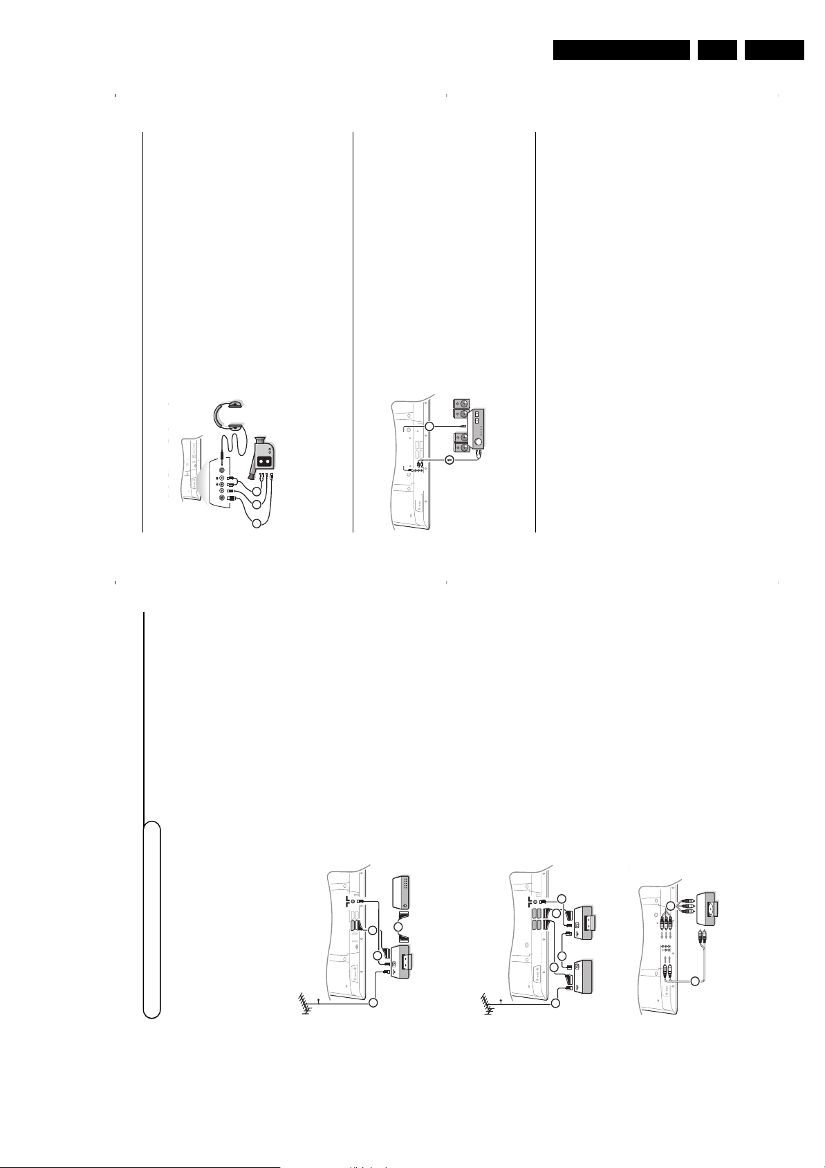
Multi channel Surround receiver
&
Connect the audio cable to the multi channel Surround receiver
and to
AUDIO OUT L
and
R
at the bottom of your TV 1.
é
If you want the loudspeakers of your TV to act as centre
speaker, also connect an audiocable to the multi channel
Surround receiver and to the
CENTRE IN
at the bottom of
your TV 2.
“
Select
Centre Input On
in the Source menu. See p. 9.
The loudspeakers of the TV will now only produce centre
sound, the loudspeakers connected to the audio receiver will
produce Surround Sound.The volume has to be controlled via
the multi channel Surround receiver.
Note: No sound will be heard when a TV channel or external source is
blocked via the Child lock menu (see p. 12).
S•VIDEO
VIDEO AUDIO
LR
L
R
2
CENTRE IN
OUT
AUDIO
Front connections
Camera or Camcorder
&
Connect your camera or camcorder as shown.éConnect to
VIDEO
2 and
AUDIO L
3 for mono
equipment. For stereo equipment also connect
AUDIO R
3.
S-VHS quality with an S-VHS camcorder is obtained by
connecting the S-VHS cables with the
S-VIDEO
input 1 and
audio inputs 3.
Do not connect cable 1 and 2 at the same time.This may cause
picture distortion !
Headphone
&
Insert the plug into the headphone socket L as shown.éPress ¬ on the remote control to switch off the internal
loudspeakers of the TV.
The headphone impedance must be between 8 and 4000 Ohm.The
headphone socket has a 3.5 mm jack.
In the Sound menu select
Headphone volume
to adjust the
headphone volume.
ANTENNA
SERVICE
75
S•VIDEO
VIDEOAUDIO
LR
S•VHSVH
S
AUDIO
A
U
D
I
O
VID
EO I
N
VID
EOIN
S•VHS
AUDIO
VIDEO IN
L
R
1 2
3
L
Press the v key on the remote control repeatedly, or select Source in the Setup menu (see p. 9) to
select
EXT1
,
EXT2
,
EXT3
,
EXT4
,
YPbPr
,
FRONT
or
VGA
according to where you connected your
equipment.
Remark : Most equipment (decoder, recorder) carries out the switching itself, when it is switched on.
To select connected equipment
17
There is a wide range of audio and video equipment that can be connected to your TV.
The following connection diagrams show you how to connect them.
Note:
EXT1
can handle CVBS and RGB;
EXT2
CVBS, Y/C and RGB;
EXT3
and
4
CVBS;
EXT5
Y-Pb-Br 480p, 576p,
1080i;
VGA IN
can hancle VGA, SVGA, XGA and 480p, 576p, 1080i.
It is preferred to connect peripherals with RGB output to
EXT1
or
EXT2
as RGB provides a better picture quality.
Note: If your recorder is provided with the EasyLink function, it should be connected to
EXT2
to benefit from the
EasyLink functionality.
Recorder (
VCR
-
DVD
+
RW
)
Note: Do not place your recorder too close to the screen as some recorders may be susceptible for signals out of the
display. Keep a minimum distance of 0,5 m to the screen.
EXT 1
Pr
ANTENNA
75
S•VIDEO
VIDEO AUDIO
LR
EXT 2
VCR 1 DECODER
4
3
2
CABLE
1
ANTENNA
75
S•VIDEO
VIDEO AUDIO
LR
EXT
CABLE
1
2
VCR 1
4
3
5
Connect Peripheral Equipment
Connect the aerial cables 1, 2 and, to obtain the
optimum picture quality, eurocable 3 as shown.
If your recorder does not have a euroconnector, the
only possible connection is via the aerial cable.You will
therefore need to tune in your recorder’s test signal and
assign it programme number 0 or store the test signal
under a programme number between 90 and 99, see
Manual installation, p. 6.
See the handbook of your recorder.
Decoder and Recorder
Connect a eurocable 4 to your decoder and to the
special euroconnector of your recorder. See also the
recorder handbook. See Decoder, p. 9. You can also
connect your decoder directly to
EXT1
or
2
with a
eurocable.
Other equipment
(satellite receiver, decoder, DVD, games, etc.)
&
Connect the aerial cables 1, 2 and 3 as shown
(only if your peripheral has TV aerial in-/output).
Connect your equipment with a eurocable 4 or 5 to
one of the euroconnectors
EXT1
,
2
,
3
or
4
to obtain a
better picture quality.
é
Look for the test signal of your peripheral in the same
way as you do for a recorder.“Make a selection in the Setup, Source menu, p. 9.
S•VIDEO
VIDEO AUDIO
LR
DVD
L
R
Y
Pb
Pr
2
1
EXT 5
DVD player
With Component Video Output Connectors
(EXT5/YPbPr
)
&
Connect the three separate component video cables to
the DVD player’s
Y
,
U
(Pb) and
V
(Pr) jacks and to the
Y, Pb and Pr jacks on the TV.
é
Connect the audio cable to the DVD player’s
AUDIO L
and
R
jacks and to the
L
and
R
audio
EXT5
jacks on the
TV.
EN 15FTL13E AA & AB 3.
Page 16
EN 16 FTL13E AA & AB3.
20
Recorder or DVD with EasyLink
The recorder (VCR or DVD+RW) or DVD can
be operated with the remote control via the
Recorder
or
DVD
menu on screen.
&
Press the
MENU
key on the remote control.
é
Select the
Recorder
or
DVD
menu with the
cursor up/down.
“
Press the cursor left/right, up/down to select
one of the recorder or DVD functions.
The key ® for recording can be operated in the TV
mode.
If your EasyLink recorder has the system standby
function, when you press the B key for 3 seconds,
both TV and the recorder are switched to standby.
Ò p ‡ π † ® Ï
Rwd Play Stop Play Ffw Rec Eject
Recorder
Ò p ‡ π † Ï
Prev. Play Stop Play Next Eject
DVD
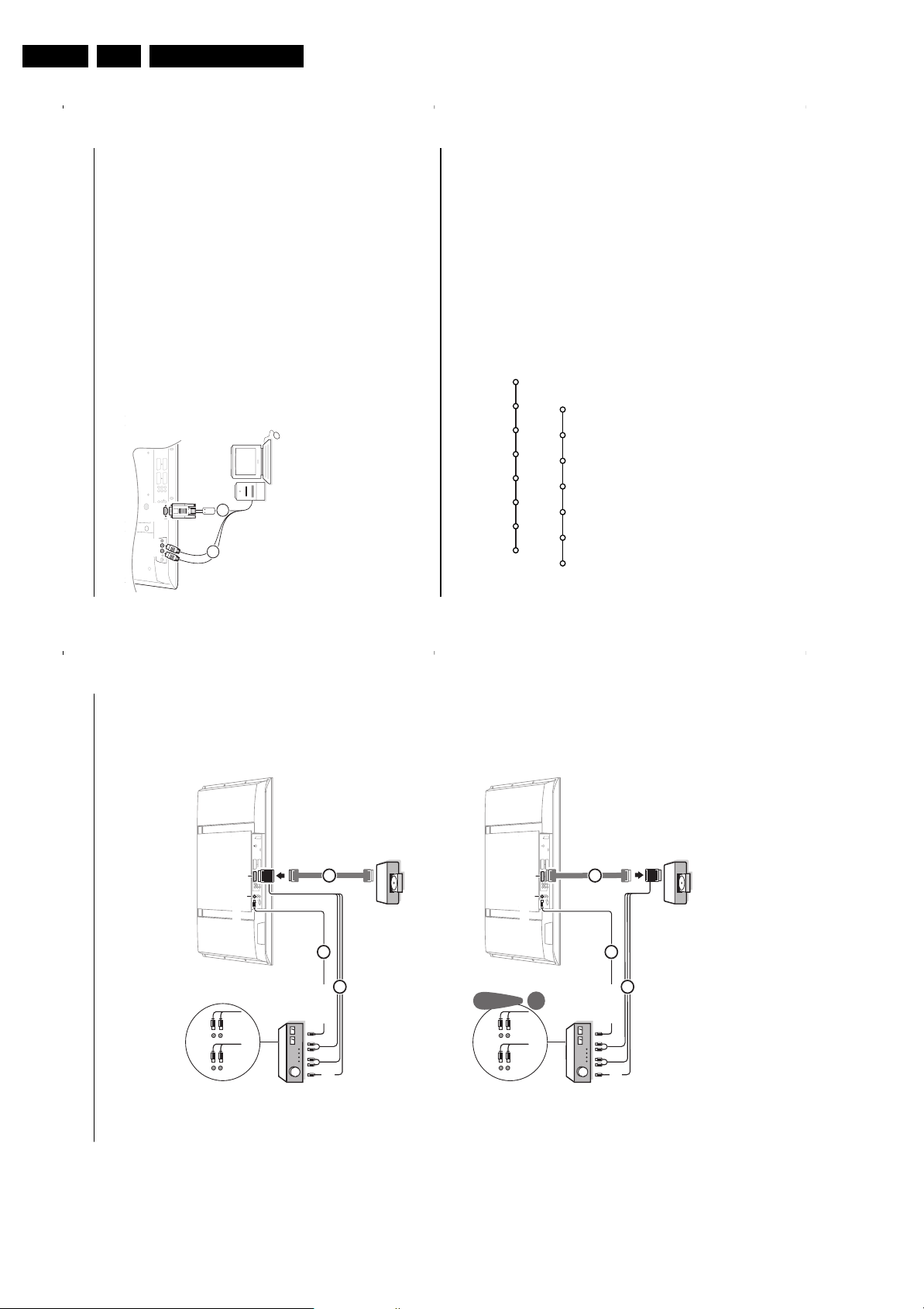
Connect your computer
EXT 2
AUDIO
RECEIVER
EXT 5
EXT 1
EXT 4
EXT 3
CINEMA LINK
Y
Pb
PrR
L
AUDIO
NO
FUNCTION
AUDIO
OUT
CENTRE
IN
MAINS
ANTENNA
SERVICE
75
R
L
S•VIDEO
VIDEO
VGA
IN
AUDIO
L
R
1
2
&
Connect one end of a VGA cable 1 to the video card
of the computer and the other end to the
VGA
connector at the bottom of the TV.
Fix the connectors firmly with the screws on the plug.
é
In case of a Multimedia computer,connect the audio
cable 2 to the audio outputs of your Multimedia
computer and to the
AUDIO R
(right) and
L
left)
inputs
of the side panel.
The
VGA IN
connector allows the following TV and
monitor display modes:
EDTV 640/720 x 480p
720 x 576p
HDTV 1920 x1080i
VGA 640 x 480 60 Hz
SVGA 800 x 600 56 Hz
XGA 1024 x 768 60 Hz
Note:
If possible, use the XGA1024x768@60Hz video mode to
obtain the best image quality for your LCD monitor.
19
See the separate supplied Cinema Link instruction manual.
Attention: the sound info on screen will not correspond with the actual sound reproduction.
Cinema Link surround receiver
OUT
U
O
A
U
O
OR
Directions for Use
MAINS
75
ANTENNA
VCR
TV
SERVICE
EXT 4
EXT 3
EXT 1
CINEMA LINK
2
EXT
YPbPrR
L
NO
EXT 5
AUDIO
FUNCTION
L
R
OUT
AUDIO
IN
IN
VGA
CENTRE
IN
VCR
IN
TV
3
Recorder
DVD/
2
1
ENTRE
DI
A
LINK
INEM
VCR
TV
2
EXT
IN
CENTRE
MAINS
75
ANTENNA
SERVICE
EXT 4
EXT 3
EXT 1
CINEMA LINK
YPbPrR
L
NO
EXT 5
AUDIO
FUNCTION
L
R
OUT
AUDIO
IN
VGA
3
Recorder
DVD/
2
1
IN
TV
IN
VCR
CENTRE OUT
DI
A
LINK
CINEMA
Page 17
Directions for Use
22
Tips
Care of the screen
Do not rub or strike the screen with anything hard as this may scratch, mar, or
damage the screen permanently.
Unplug the set before cleaning the screen. dust the TV by wiping the screen and
the cabinet with a soft, clean cloth.If the screen requires additional cleaning, use
a clean, damp cloth;do not use liquid cleaners or aerosol cleaners.
Poor Picture • Have you selected the correct TV system in the manual installation menu?
• Is your TV or house aerial located too close to loudspeakers, non-earthed audio
equipment or neon lights, etc.?
• Mountains or high buildings can cause double pictures or ghost images.
Sometimes you can improve the picture quality by changing the direction of the
aerial.
• Is the picture or teletext unrecognisable? Check if you have entered the correct
frequency. See Installation, Manual installation, p. 6.
• Are brightness, sharpness and contrast out of adjustment? Select Factory settings in
the Setup, General menu, p. 8.
No Picture • Are the supplied cables connected properly ? (The aerial cable to the TV, the
other aerial to your recorder, the VGA cables to the display, the power cables.)
• Has the child lock been switched off ?
• Is your PC switched on ?
• Do you see a black screen and the indicator in front of the TV lights up green,
this means that the display mode is not supported. Switch your VGA-source to a
correct mode.
• In case of weak or bad signal, consult your dealer.
Digital distortion The low quality of some digital picture material may be the cause of digital image
distortion. In this case select the Soft setting using the Picture menu,Smart Picture,
without changing the picture settings manually.
No sound • No sound on any channel? Check the volume isn’t at minimum.
• Is the sound interrupted with the mute key
¬
?
No solution found Switch your TV off and then on again once. Never attempt to repair a defective
for your picture or TV yourself. Check with your dealer or call a TV technician.
sound problem ?
Menu Have you selected the wrong menu? Press the menu key again to exit from the
menu.
NEX
TV
IEW
Orange indicator on front of the TV during standby / No
NEX
TV
IEW
info:
See Acquisition and updating of
NEX
TV
IEW
information, p. 14.
Displayed time is wrong:
The broadcaster on programme number one does not transmit the correct local
date and time. Use Reshuffle in the installation menu to place another broadcaster
on programme number one.
Remote control • Check if the remote control is in the correct mode.
• If your TV no longer responds to the remote control, the batteries may be dead.
• You can still use the
MENU/OK
key and the -/+ keys on top of your TV.
Standby Your TV consumes energy in the standby mode. Energy consumption contributes
to air and water pollution. Power consumption: 2 W.
No stable or not Check if you have selected the correct VGA mode in your PC. See the separate
synchronised VGA instruction manual with the monitor.
picture
Miscellaneous . Ambient temperature: + 5~ + 35°C
. Mains: 50/60 Hz Auto Voltage ranging from 198 V to 264 V
. Power consumption:around 170 W
. Standby consumption: 1 W
. Weight (excl. packaging): 17 kg
. Dimensions (wxhxd): 891x489x110
Tips
21
Audio- and video equipment keys
Record with your recorder with EasyLink
This system remote control operates the following Philips equipment:TV,VCR,
DVD, SAT (RC5),AMP (+TUNER), CD;
Press the
Select
key to operate any of the equipment indicated in the display.
Another device can be selected by pressing Select repeatedly within 2 seconds.The
led will blink slowly to indicate the device.
Press one of the keys on the remote control to operate the peripheral equipment.
To return to TV mode press Select while the led is blinking.
When no action is taken within 60 seconds, the remote goes back to TV mode.
Note: When the
Select
key is pressed and hold for more than 2 seconds, the RC5/RC6
system select command is transmitted.
B
b
¬
+
-
V
+
-
P
v
b
i
0
h
q
Select
VCR DVD SAT AMP CD
MENU
OK
123
456
789
0
Ò
®
‡π
†
Active Control
S
®
®
®
®
æ
B to switch to standby
S for pause (
VCR
,
DVD
,
CD)
® for record
Ò for rewind (
VCR
,
CD
);
search down (
DVD
,
AMP
)
‡ for stop
π for play
† for fast forward (
VCR
,
CD
);
search up (
DVD/AMP
)
æ to select your choice of subtitle
language (
DVD
);
RDS news/TA (
AMP
);
to shuffle play (
CD
)
b to select a
DVD
title;
RDS display (
AMP
);
info on screen (
CD
)
i display information
MENU
to switch the menu on or off
- P +
for chapter, channel, track
selection
0 to 9 digit entry
0 tape index (
VCR
),
select a DVD chapter,
select a frequency (
AMP
)
U VCR timer
Q surround on/off (
AMP
,
CD)
cursor up/down
to select the next or the
previous disc (
CD)
cursor left/right
to select the previous or
following track (
CD
)
search up/down (
AMP
)
In TV mode, it is possible to start a direct recording of the programme which is being displayed on the TV
screen. Continue to press the ® record key on the remote control for more than 2 seconds.
Note: Switching programme numbers on your TV does not disturb recording !
When recording a programme from a peripheral connected to
EXT 1
,
EXT 3, EXT 4,EXT 5
or
FRONT
, you can
not select another TV programme on the screen.
Attention:
Recording from
EXT 5
will only have black and white pictures !
Additionally the DVD, SAT and CD indicator can be programmed to operate the
DVD-R, SAT (RC6), CD-R instead.
&
Press the
Select
key repeatedly until no LED is lit.
é
To program
DVD-R
, press the
OK
key + digit 2.
To program
SAT (RC6)
, press the
OK
key + digit 4.
To program
CD-R
, press the
OK
key + digit 6.
From now on, when the corresponding (
DVD
,
SAT
,
CD
) indicator is selected,
the remote control will operate your DVD-R, SAT (RC6) or CD-R.
Note:To return to the modes programmed in the factory, either remove the batteries for a
few minutes, or press the
OK
key + digit 1 (DVD mode); or + digit 3 (SAT-RC5) or +
digit 5 (CD mode).
EN 17FTL13E AA & AB 3.
Page 18

EN 18 FTL13E AA & AB3.
Table of TV frequencies.
Frequenztabelle der Fernsehsender.
Liste des fréquences des émetteurs.
Frequentietabel TV-Zenders.
Tabella delle frequenze delle trasmittenti.
Lista de las frecuencias de las emisoras.
Lista das frequências dos emissores.
Liste over TV senderne.
Tabell over TV-frekvenser.
Tabell över TV-frekvenser.
TV-taajuustaulukko.
Kατάλογος συχνοτήτων ποµπών.
Spisok hastot peredathikov.
A televizió−adóállomások frekvenciáinak a listája.
Lista częstotliwości stacji nadawczych.
Seznam frekvenčních pásem vysílačů.
Zoznam frekvenčných pásiem vysielačov.
GB
The frequencies used by a cable company may differ from the
frequencies on the table. Consult your cable company or your
dealer for detailed information.
D
In Kabelfernsehanlagen können Abweichungen von den in den
Frequenztabellen aufgeführten Frequenzen vorkommen. Bitte
wenden Sie sich an Ihren Fachhändler oder Ihre
Kabelfernsehgesellschaft, die Ihnen die zutreffenden Frequenzen
mitteilt.FLes fréquences utilisées par une société de télédistribution
peuvent être différentes de celles sur la liste des fréquences.
Consultez votre société de télédistribution ou votre revendeur
pour des informations plus détailées.
NL
De frequenties die gebruikt worden door een kabelmaatschappij
kunnen verschillen van deze op de tabel. Raadpleeg uw
kabelexploitant of uw handelaar voor meer informatie.
I
Le frequenze usate per una società di teledistribuzione possano
essere differenti di quelle nella tabella. Consultate la società di
teledistribuzione o il vostro rivenditore per informazione specifica.
E
Las frecuencias utilizadas por las empresas de distribución de
señal por cable, pueden ser diferentes de las que se encuentran
en esta tabla. Consulte con su compañia de distribución de
televisión por cable o con su distribuidor para que le proporcionen
una información más detallada.
P
As frequências utilizadas por uma sociedade de teledistribuição
podem ser diferentes das indicadas na lista de frequências.
Consultar a sociedade de teledistribuição ou o vendedor para
informações mais detalhadas.
DK
Frekvenser benyttet af kabel operatører kan være afvigende fra
disse, kantakt deres kabel operatør eller forhandler for næmere
informa-tion.NFrekvensene som benyttes pa et kabelnett kan avvike fra de
som er oppfört i tabellen. Kontakt ditt kabel-TV selskap eller din
forhandler for næmere opplysninger.SFrekvenserna som används i kabel-TV-näten kan avvika från
frekvenserna i tabellen. Kontakta ditt kabel-TV-bolag eller din
radiohandlare för vidare information.
SF
Kaapeliyhtiöden käyttämät taajuudet voivat poiketa taulukossa
olevista taajuuksista. Tarkat tiedot saat kaapeliyhtiösta tai myyjältä.
GR
Οι συχντητες που χρησιµοποιούνται απ µια εταιρεία τηλεµετάδοσης
είναι δυνατν να είναι διαφορετικές απ αυτές που περιέχει ο κατάλογος.
(Συµβουλευθείτε την εταιρεία τηλεµετάδοσης ή τον πωλητή για
λεπτοµερέστερες πληροφορίες).
CEI
Hastoty na kotoryx peredaòt telakampaniä mogut
otlihatæsä ot hastot na dannoj tablice. (Obratitæsä k
Vaπej telekampanii ili Vaπemu prodavcu za
dopolnitelænoj informaciej.
H
Egy televizió−adóállomás sugárzáshoz használt frekvenciatar−
tományai lehetnek a táblázatban közöltektől eltérőek is. (Abban
az esetben, ha bővebb információkra van szüksége, forduljon az
eladóhoz.)PLOperator sieci telewizyjnej może stosować inne częstotliwości,
niż te, które figurują na tablicy (bardziej szczegółowych infor−
macji na ten temat zasięgnąć u operatora lub sprzedawcy).
CZ
Frekvence používané některými televizními společnostmi se
mohou lišit od údajů uvedených v tomto seznamu. Informujte se
blíže u příslušné společnosti nebo v prodejně, kde jste televizor
koupili.SKFrekvencie používané niektorými spoločnosami televízneho
prenosu sa môžu liši od údajov uvedených v tomto zozname.
Informujte sa bližšie u príslušnej spoločnosti alebo v predajni,
kde ste televízor kúpili.
EUROPE
CH ..FREQ (MHz)
E2.............48.25
E3.............55.25
E4.............62.25
E5...........175.25
E6...........182.25
E7...........189.25
E8...........196.25
E9...........203.25
E10.........210.25
E11.........217.25
E12.........224.25
S1...........105.25
S2...........112.25
S3...........119.25
S4...........126.25
S5...........133.25
S6...........140.25
S7...........147.25
S8...........154.25
S9...........161.25
S10.........168.25
S11.........231.25
S12.........238.25
S13.........245.25
S14.........252.25
S15.........259.25
S16.........266.25
S17.........273.25
S18.........280.25
S19.........287.25
S20.........294.25
H1 ..........303.25
H2 ..........311.25
H3 ..........319.25
H4 ..........327.25
H5 ..........335.25
H6 ..........343.25
H7 ..........351.25
H8 ..........359.25
H9 ..........367.25
H10 ........375.25
H11 ........383.25
H12 ........391.25
H13 ........399.25
H14 ........407.25
H15 ........415.25
H16 ........423.25
H17 ........431.25
H18 ........439.25
H19 ........447.25
21...........471.25
22...........479.25
23...........487.25
24...........495.25
25...........503.25
26...........511.25
27...........519.25
28...........527.25
29...........535.25
30...........543.25
31...........551.25
32...........559.25
33...........567.25
34...........575.25
35...........583.25
36...........591.25
37...........599.25
38...........607.25
39...........615.25
40...........623.25
41...........631.25
42...........639.25
43...........647.25
44...........655.25
45...........663.25
46...........671.25
47...........679.25
48...........687.25
49...........695.25
50...........703.25
51...........711.25
52...........719.25
53...........727.25
54...........735.25
55...........743.25
56...........751.25
57...........759.25
58...........767.25
59...........775.25
60...........783.25
61...........791.25
62...........799.25
63...........807.25
64...........815.25
65...........823.25
66...........831.25
67...........839.25
68...........847.25
69...........855.25
E-EUROPE
CAN..FREQ (MHz)
R1 ..........49.75
R2 ..........59.25
R3 ..........77.25
R4 ..........85.25
R5 ..........93.25
R 6 .......175.25
R 7 .......183.25
R 8 .......191.25
R 9 .......199.25
R10 ......207.25
R11 ......215.25
R12 ......223.25
S1 ........105.25
S2 ........112.25
S3 ........119.25
S4 ........126.25
S5 ........133.25
S6 ........140.25
S7 ........147.25
S8 ........154.25
S9 ........161.25
S10 ......168.25
S11 ......231.25
S12 ......238.25
S13 ......245.25
S14 ......252.25
S15 ......259.25
S16 ......266.25
S17 ......273.25
S18 ......280.25
S19 ......287.25
S20 ......294.25
H1 ........303.25
H2 ........311.25
H3 ........319.25
H4 ........327.25
H5 ........335.25
H6 ........343.25
H7 ........351.25
H8 ........359.25
H9 ........367.25
H10 ......375.25
H11 ......383.25
H12 ......391.25
H13 ......399.25
H14 ......407.25
H15 ......415.25
H16 ......423.25
H17 ......431.25
H18 ......439.25
H19 ......447.25
21.........471.25
22.........479.25
23.........487.25
24.........495.25
25.........503.25
26.........511.25
27.........519.25
28.........527.25
29.........535.25
30.........543.25
31.........551.25
32.........559.25
33.........567.25
34.........575.25
35.........583.25
36.........591.25
37.........599.25
38.........607.25
39.........615.25
40.........623.25
41.........631.25
42.........639.25
43.........647.25
44.........655.25
45.........663.25
46.........671.25
47.........679.25
48.........687.25
49.........695.25
50.........703.25
51.........711.25
52.........719.25
53.........727.25
54.........735.25
55.........743.25
56.........751.25
57.........759.25
58.........767.25
59.........775.25
60.........783.25
61.........791.25
62.........799.25
63.........807.25
64.........815.25
65.........823.25
66.........831.25
67.........839.25
68.........847.25
69.........855.25
FRANCE
CAN..FREQ (MHz)
2..............55.75
3..............60.50
4..............63.75
5..............176.0
6..............184.0
7..............192.0
8..............200.0
9..............208.0
10............216.0
B............116.75
C............128.75
D............140.75
E............159.75
F............164.75
G ...........176.75
H............188.75
I.............200.75
J............212.75
K............224.75
L............236.75
M...........248.75
N ...........260.75
O ...........272.75
P............284.75
Q ...........296.75
H1..........303.25
H2..........311.25
H3..........319.25
H4..........327.25
H5..........335.25
H6..........343.25
H7..........351.25
H8..........359.25
H9..........367.25
H10........375.25
H11........383.25
H12........391.25
H13........399.25
H14........407.25
H15........415.25
H16........423.25
H17........431.25
H18........439.25
H19........447.25
21..........471.25
22..........479.25
23..........487.25
24..........495.25
25..........503.25
26..........511.25
27..........519.25
28..........527.25
29..........535.25
30..........543.25
31..........551.25
32..........559.25
33..........567.25
34..........575.25
35..........583.25
36..........591.25
37..........599.25
38..........607.25
39..........615.25
40..........623.25
41..........631.25
42..........639.25
43..........647.25
44..........655.25
45..........663.25
46..........671.25
47..........679.25
48..........687.25
49..........695.25
50..........703.25
51..........711.25
52..........719.25
53..........727.25
54..........735.25
55..........743.25
56..........751.25
57..........759.25
58..........767.25
59..........775.25
60..........783.25
61..........791.25
62..........799.25
63..........807.25
64..........815.25
65..........823.25
66..........831.25
67..........839.25
68..........847.25
69..........855.25
ITALY
CAN..FREQ (MHz)
A..............53.75
B ..............62.25
C ..............82.25
D............175.25
E ............183.75
F.............192.25
G............201.25
H............210.25
H1..........217.25
S1 ..........105.25
S2 ..........112.25
S3 ..........119.25
S4 ..........126.25
S5 ..........133.25
S6 ..........140.25
S7 ..........147.25
S8 ..........154.25
S9 ..........161.25
S10 ........168.25
S11 ........231.25
S12 ........238.25
S13 ........245.25
S14 ........252.25
S15 ........259.25
S16 ........266.25
S17 ........273.25
S18 ........280.25
S19 ........287.25
S20 ........294.25
H1..........303.25
H2..........311.25
H3..........319.25
H4..........327.25
H5..........335.25
H6..........343.25
H7..........351.25
H8..........359.25
H9..........367.25
H10........375.25
H11........383.25
H12........391.25
H13........399.25
H14........407.25
H15........415.25
H16........423.25
H17........431.25
H18........439.25
H19........447.25
21...........471.25
22...........479.25
23...........487.25
24...........495.25
25...........503.25
26...........511.25
27...........519.25
28...........527.25
29...........535.25
30...........543.25
31...........551.25
32...........559.25
33...........567.25
34...........575.25
35...........583.25
36...........591.25
37...........599.25
38...........607.25
39...........615.25
40...........623.25
41...........631.25
42...........639.25
43...........647.25
44...........655.25
45...........663.25
46...........671.25
47...........679.25
48...........687.25
49...........695.25
50...........703.25
51...........711.25
52...........719.25
53...........727.25
54...........735.25
55...........743.25
56...........751.25
57...........759.25
58...........767.25
59...........775.25
60...........783.25
61...........791.25
62...........799.25
63...........807.25
64...........815.25
65...........823.25
66...........831.25
67...........839.25
68...........847.25
69...........855.25
Directions for Use
Personal Notes:
Page 19
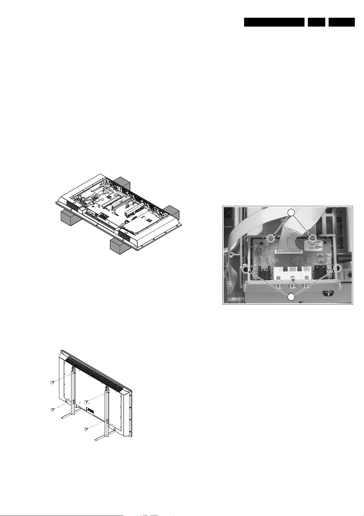
4. Mechanical Instructions
Mechanical Instructions
EN 19FTL13E AA & AB 4.
Index of this chapter:
4.1 Service Positions
4.2 Assy/PWB Removal
4.3 Set Re-assembly
Notes:
• Figures below can deviate slightly from the actual situation,
due to the different set executions.
• Follow the disassemble instructions in described order.
4.1 Service Positions
First, put the TV set in its service position. Therefore, place it
upside down on a table top (use a protection sheet or a foam
cushion).
4.1.1 The Foam Bars
does not take much space, has no risk of over heating, and/or
falling. The stands can be mounted and removed quickly and
easily with use of the provided screws, which can be tightened
and loosened manually without the use of tools
Caution: Only use the screws provided, otherwise it is possible
to damage the monitor inside.
4.2 Assy/PWB Removal
4.2.1 Rear Cover
Warning: Disconnect the mains power cord before you remove
the rear cover.
First, unscrew the rear cover:
1. Remove the screws that secure the rear cover. The screws
are located at the top, bottom, left and right side, also there
are three deeper located screws next to the stands.
2. Lift the rear cover from the cabinet. Make sure that wires
and flat foils are not damaged during cover removal.
4.2.2 Side I/O Panel
2
CL 36532051_002.eps
Figure 4-1 Foam bars
The foam bars (order code 3122 785 90580) can be used for
all types and sizes of Flat TVs. By laying the plasma or LCD TV
flat on the (ESD protective) foam bars, a stable situation is
created to perform measurements and alignments. By first
placing a mirror flat on the table under the TV you can easily
see if something is happening on the screen.
The stand is also handy to replace the screen.
4.1.2 The Aluminium Stands
190603
1
CL 36532064_050.eps
161003
Figure 4-3 Side I/O panel
1. Disconnect the cable of the panel
2. To replace the complete bracket, remove the two fixing
screws (1) on either side of the panel.
3. To get the panel out, push the two brackets out and lift the
panel off.
4. Remove the panel.
CL 36532051_001.eps
040703
Figure 4-2 Aluminium stands
The aluminium stands (order code 3122 785 90480) can also
be used to do measurements and alignments, also they are
very suitable to perform duration tests. With this stands the set
Page 20
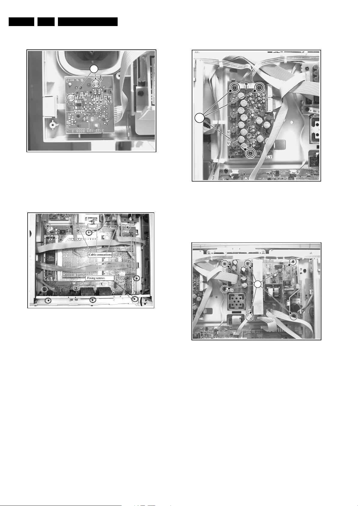
EN 20 FTL13E AA & AB4.
Mechanical Instructions
4.2.3 Main switch/LED panel
1
Figure 4-4 Main switch/LED panel
1. Disconnect the cable on the rear of the panel.
2. Remove the two fixing screws (1) as shown on the photo.
4.2.4 Small Signal Panel
CL 36532064_051.eps
161003
4.2.5 Audio Amplifier
1
Figure 4-6 Audio Amplifier
1. Disconnect all cables from the panel.
2. Remove the fixing screws (1) of the panel.
CL 36532064_053.eps
161003
CL 36532053_091.eps
Figure 4-5 Small Signal Panel
1. Disconnect all cables from the panel.
2. Caution: The connectors of the LVDS cable are very
fragile, be careful not to damage them.
3. Remove the fixing screws of the panel.
301003
4.2.6 Auxiliary Supply
Figure 4-7 Auxiliary Supply
1. Disconnect all cables from the panel.
2. Remove the fixing screws (1) of the panel.
1
CL 36532064_054.eps
161003
Page 21
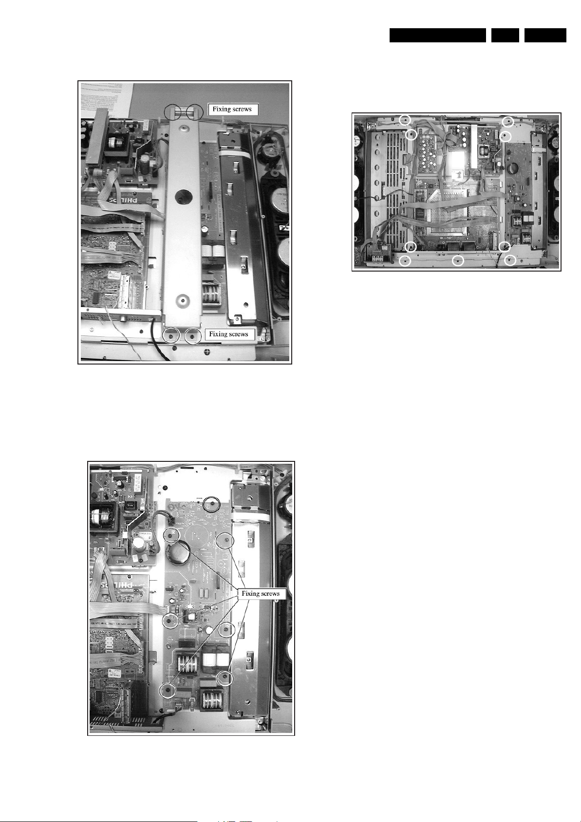
Mechanical Instructions
EN 21FTL13E AA & AB 4.
4.2.7 Main Power Supply
Figure 4-8 Wall mounting bracket
1. Remove the screws on both the top and bottom of the
mounting bracket.
2. Remove the bracket before accessing the Main Power
Supply panel.
CL 36532053_094.eps
301003
1. Disconnect the cables from the panel.
2. Remove the fixing screws on each side of the panel.
4.2.8 LCD Panel
Figure 4-10 LCD Display
Make sure that the power is switched “off” and that the
necessary cables are disconnected.
To replace the LCD panel (including the backlight), please
remove all the panels first (including the two mounting
brackets), as mentioned above.
1. Remove the five fixing screws on the border of the panel
with a no. 10 Torx screwdriver.
2. Remove the four fixing screws on the panel with a no. 20
Torx screwdriver.
3. Lift the LCD panel including the backlights out of the frame.
4.3 Set Re-assembly
To re-assemble the whole set, execute all processes in reverse
order.
Notes:
• As soon as you have removed the plastic back cover, you
must replace the speaker-box sealing foam (12nc: 3104
303 10791). This, to ensure that the loudspeakers are
airtight. Do not stretch the foam during mounting. Pay
special attention to the corners, to make sure that the foam
is not stretched and that it is pushed in the corners.
• While re-assembling, make sure that all cables are placed
and connected in their original position
CL 36532053_096.eps
301003
Figure 4-9 Main Power Supply
CL 36532053_095.eps
301003
Page 22

EN 22 FTL13E AA & AB5.
Service Modes, Error Codes, and Fault Finding
5. Service Modes, Error Codes, and Fault Finding
Index of this chapter:
5.1 Test Points
5.2 Service Modes
5.3 Problems and Solving Tips (related to CSM)
5.4 ComPair
5.5 Error Codes
5.6 The Blinking LED Procedure
5.7 Protections
5.8 Repair tips
5.9 Software Downloading
5.1 Test Points
The chassis is equipped with test points printed on the circuit
board assemblies.
Perform measurements under the following conditions:
• Service Default Mode.
• Video: colour bar signal.
• Audio: 3 kHz left, 1 kHz right.
5.2 Service Modes
Service Default Mode (SDM) and Service Alignment Mode
(SAM) offer several features for the service technician, while
the Customer Service Mode (CSM) is used for communication
between a Philips Customer Care Centre (P3C) and a
customer.
There is also the option of using ComPair, a hardware interface
between a computer (see requirements below) and the TV
chassis. It offers the ability of structured troubleshooting, test
pattern generation, error code reading, software version
readout, and software upgrading.
Minimum requirements: a Pentium processor, Windows 95/
98, and a CD-ROM drive (see also paragraph “ComPair”).
5.2.1 Service Default Mode (SDM)
Purpose
• To create a pre-defined setting, to get the same
measurement results as given in this manual.
• To override SW protections.
• To start the blinking LED procedure.
Specifications
• Tuning frequency: 475.25 MHz for PAL/SECAM.
• Colour system: SECAM L for France or PAL B/G for the
rest of Europe.
• All picture settings at 50 % (brightness, colour, contrast).
• All sound settings at 50 %, except volume at 25 %.
• All service-unfriendly modes (if present) are disabled, like:
– (Sleep) timer.
– Child/parental lock.
–Blue mute.
– Automatic volume limiter (AVL).
– Auto switch-off (when no video signal was received for
10 minutes).
– Skip/blank of non-favourite pre-sets.
– Smart modes.
– Auto store of personal presets.
– Auto user menu time-out.
How to enter SDM
Use one of the following methods:
• Use the standard RC-transmitter and key in the code
“062596”, directly followed by the “MENU” button.
Note: It is possible that, together with the SDM, the main
menu will appear. To switch it off, push the “MENU” button
again.
• Short for a moment the two solder pads (item 9018) on the
SSP, with the indication “SDM”. Activation can be
performed in all modes, except when the set has a problem
with the main microprocessor.
Caution: If the SDM is entered via the pins, all the
software-controlled protections are de-activated.
• Use the DST-emulation feature of ComPair.
• Use the “DEFAULT” button on the Dealer Service Tool
(RC7150).
After entering this mode, “SDM” will appear in the upper right
corner of the screen.
How to navigate
When you press the “MENU” button on the RC transmitter, the
set will toggle between the SDM and the normal user menu
(with the SDM mode still active in the background).
How to exit SDM
Use one of the following methods:
• Switch the set to STANDBY via the RC-transmitter.
• Press the “EXIT” button on the DST.
• Via a standard customer RC-transmitter: key in “00”sequence.
5.2.2 Service Alignment Mode (SAM)
Purpose
• To perform (software) alignments.
• To change option settings.
• To easily identify the used software version.
• To view operation hours.
• To display (or clear) the error code buffer.
Specifications
• Operation hours counter.
• Software version.
• Option settings.
• Error buffer reading and erasing.
• Software alignments.
How to enter SAM
Use one of the following methods:
• Via a standard RC transmitter: key in the code “062596”
directly followed by the “OSD [i+]” button. After entering
SAM with this method a service warning will appear on the
screen, you can continue by pressing any digit key on the
RC.
• Short for a moment the two solder pads (item 9017) on the
SSP with the indication "SAM". Depending on the software
version, it is possible that a service warning will appear.
You can continue by pressing any digit key on the RC.
• Use the DST-emulation feature of ComPair.
• Press the ALIGN button on the DST while the set is in the
normal operation
After entering this mode, “SAM” will appear in the upper right
corner of the screen.
Contents of SAM:
• OPERATION HOURS. Displays the accumulated total of
operation hours (not the standby hours).
• HARDWARE INFO.
– ROM VERSION. Displays the date of the software and
the software version of the ROM (example:
TL13EU_1.0_01234 = AAAABB_X.Y_NNNNN).
• AAAA= the chassis name.
Page 23
Service Modes, Error Codes, and Fault Finding
EN 23FTL13E AA & AB 5.
• BB= the region: EU= Europe, AP= Asia Pacific
PAL/Multi, AN= Asia Pacific NTSC, US= USA, LT=
LATAM.
• X.Y= the software version, where X is the main
version number (different numbers are not
compatible with one another) and Y is the sub
version number (a higher number is always
compatible with a lower number).
• NNNNN= last five digits of 12nc code software.
– SW VERSION EPLD. Displays the software version of
the EPLD.
• ERRORS. (followed by maximal 10 errors). The most
recent error is displayed at the upper left (for an error
explanation see paragraph “Error Codes”).
• DEFECTIVE MODULE. Here the module that generates
the error is displayed. If there are multiple errors in the
buffer, which are not all generated by a single module,
there is probably another defect. It will then display the
message “UNKNOWN” here.
• RESET ERROR BUFFER. When you press the “OK”
button, the error buffer is reset.
• ALIGNMENTS. This will activate the “ALIGNMENTS” submenu.
• DEALER OPTIONS. Extra features for the dealers.
• SERVICE OPTIONS. Extra features for Service.
• INITIALISE NVM. When an NVM was corrupted (or
replaced) in the former EM3 chassis, the microprocessor
replaces the content with default data (to assure that the
set can operate). However, all pre-sets and alignment
values are gone now, and option numbers are not correct.
Therefore, this was a very drastic way. In this chassis, the
procedure is implemented in another way: The moment the
processor recognises a corrupted NVM, the “initialise
NVM” line will be highlighted. Now, you can do two things
(dependent of the service instructions at that moment):
– Save the content of the NVM via ComPair for
development analysis, before initialising. This will give
the Philips Service department an extra possibility for
diagnosis (e.g. when Development asks for this).
– Initialise the NVM (same as in the past, however now it
happens conscious).
• STORE. All options and alignments are stored when
pressing the “OK”-button
• FUNCTIONAL TEST. All devices are tested via the “OK”
button. Eventual errors are displayed in the error buffer.
The error buffer is not erased, the content returns when this
test is terminated.
• DAILY MENUS. With the “OK” button, you can go to the
normal user menu. SAM is still active in the background.
With the “MENU” button, you return from the user menu to
SAM menu. This feature can be helpful to quickly change
some settings in the user menu.
• SW MAINTENANCE.
• UPGRADE. More info see paragraph Software
downloading.
• EVENTS. Not useful for service purposes. In case of
specific software problems, the development
department can ask for this info.
• BDM INFO. Broadcast Debug Menu info. The purpose
of this menu is to debug the broadcast, not the TV. The
menu gives an overview of what is received on the
current preset. Following items are displayed:
P r e s e t n r : -- UTC: - - : - - : --
P r e s e t n a m e : ----- LTO: - - : - - : --
Time: - - : - - : --
C N I N V M : ---- Date: - - / - - / ----
C N I F 1 : ----
C N I F 2 : ---- Time TXT: - - : - - : --
C N I V P S : ---- Time 8/30 F1: - - : - - : --
M o r n i n g P r o g : --- Date 8/30 F1: - - / - - / ----
N a m e 8 / 3 0 F 1 : ----- LTO 8/30 F1: - - : - - : --
N a m e 8 / 3 0 F 2 : -----
N a m e T X T : ----- WSS G1: - - - -
S i g n a l S t r e n g t h :--- WSS G2: - - - -
WSS G3: - - -
E P G S e r v i c e : --- WSS G4: - - -
CL 36532017_055.eps
240403
Figure 5-1 Broadcast debug menu overview
Table 5-1 Broadcast debug menu explanation
Item Source Description
Presetnr Set Presetnumber of the current
selected preset.
Presetname Set Presetname of the current se-
lected preset.
CNI NVM Broadcaster CNI number stored in NVM for
the current preset.
CNI F1 Broadcaster CNI number from transmitted
Packet 8/30 Format 1.
CNI F2 Broadcaster CNI number from transmitted
Packet 8/30 Format 2.
CNI VPS Broadcaster CNI number from transmitted
VPS line.
Morning Prog Broadcaster "ARD" or "ZDF" according to
dedicated bit in 8/30 Format 1.
Name 8/30 F1 Broadcaster Name extracted from status
message of 8/30 Format 1.
Name 8/30 F2 Broadcaster Name extracted from status
message of 8/30 Format 2.
Name TXT Broadcaster Name extracted from TXT
header.
Signal
Strength
FBX Noise figure measured for se-
lected preset.
EPG Service Set EPG Service stored in NVM for
current preset displayed as
"TXT", "MCP", "SCP", "OCP".
UTC Set UTC (Universal Time Code for-
merly known as Greenwich
Mean Time) used in the set.
LTO Set LTO (Local Time Offset) used
in the set. Used by EPG for all
Nextview displays. (= Time
TXT header - Time 8/30 F1 )
Time Set Curren t time running in the set.
Was extracted at startup, then
maintained by software.
Date Set Current date running in the set.
Was extracted at startup, then
maintained by software.
Time TXT Broadcaster TXT header time from the se-
lected preset.
Time 8/30 F1 Broadcaster UTC time from 8/30 Format 1.
Date 8/30 F1 Broadcaster Date from 8/30 Format 1.
LTO 8/30 F1 Broadcaster LTO from 8/30 Format 1.
WSS G1 Broadcaster WSS Group 1 (Aspect Ratio)
bits 0 1 2 3
WSS G2 Broadcaster WSS Group 2 (Enhanced
Services) bits 4 5 6 7
WSS G3 Broadcaster WSS Group 3 (Subtitles) bits 8
9 10
WSS G4 Broadcaster WSS Group 4 (Reserved) bits
11 12 13
How to navigate
• In SAM, you can select the menu items with the “CURSOR
UP/DOWN” key on the RC-transmitter. The selected item
will be highlighted. When not all menu items fit on the
screen, move the “CURSOR UP/DOWN” key to display the
next/previous menu items.
• With the “CURSOR LEFT/RIGHT” keys, it is possible to:
– (De) activate the selected menu item.
– Change the value of the selected menu item.
– Activate the selected submenu.
How to exit SAM
Use one of the following methods:
• Press the “MENU” button on the RC-transmitter, or
Page 24

EN 24 FTL13E AA & AB5.
Service Modes, Error Codes, and Fault Finding
• Switch the set to STANDBY via the RC-transmitter, or
• Press the “EXIT” button on the DST.
5.2.3 Customer Service Mode (CSM)
Purpose
When a customer is having problems with his TV-set, he can
call his dealer. The service technician can than ask the
customer to activate the CSM, in order to identify the status of
the set. Now, the service technician can judge the severity of
the complaint. In many cases, he can advise the customer how
to solve the problem, or he can decide if it is necessary to visit
the customer.
The CSM is a read only mode; therefore, modifications in this
mode are not possible.
How to enter CSM
Use one of the following methods:
• Press the “MUTE” button on the RC-transmitter
simultaneously with the “MENU” button on the TV (top
control) for at least 4 seconds.
• Key in the code “123654” via the standard RC transmitter.
Note: Activation of the CSM is only possible if there is no (user)
menu on the screen!
How to navigate
By means of the “CURSOR-DOWN/UP” knob on the RCtransmitter, you can navigate through the menus.
Contents of CSM
CUSTOMER SERVICE MENU 1
• SOFTWARE VERSION (example: TL13EU_1.0_01234).
Displays the built-in software version. In case of field
problems related to software, software can be upgraded
(for more details, see paragraph Software downloading).
You will find details of the software versions in the chapter
“Software Survey” of the “Product Survey - Colour
Television” publication. This publication is generated four
times a year.
• SOFTWARE VERSION EPLD. The 12NC-number of the
built-in EPLD software.
• FEATURE BOX. The 12NC-number of the built-in Feature
Box software.
• SET TYPE. This information is very helpful for a helpdesk/
workshop as reference for further diagnosis. In this way, it
is not necessary for the customer to look at the rear of the
TV-set.
• CODE 1. Gives the latest five errors of the error buffer. As
soon as the built-in diagnose software has detected an
error the buffer is adapted. The last occurred error is
displayed on the leftmost position. Each error code is
displayed as a 3-digit number. When less than 10 errors
occur, the rest of the buffer is empty (000). See also
paragraph Error Codes for a description.
• CODE 2. Gives the first five errors of the error buffer. See
also paragraph Error Codes for a description.
• VOLUME. Gives the last status of the volume as set by the
customer. The value can vary from 0 (volume is minimum)
to 100 (volume is maximum). Volume values can be
changed via the volume key on the RC-transmitter.
• BRIGHTNESS. Gives the last status of the brightness as
set by the customer. The value can vary from 0 (brightness
is minimum) to 100 (brightness is maximum). Brightness
values can be changed via the “CURSOR LEFT” and
“CURSOR RIGHT” keys on the RC-transmitter after
pressing the “MENU” button and selecting “PICTURE” and
“BRIGHTNESS”.
• CONTRAST. Gives the last status of the contrast as set by
the customer. The value can vary from 0 (contrast is
minimum) to 100 (contrast is maximum). Contrast values
can be changed via “CURSOR LEFT” and “CURSOR
RIGHT” keys on the RC-transmitter after pressing the
“MENU” button and selecting “PICTURE” and
“CONTRAST”.
CUSTOMER SERVICE MENU 2
• COLOUR. Gives the last status of the colour saturation, as
set by the customer. The value can vary from 0 (colour is
minimum) to 100 (colour is maximum). Colour values can
be changed via “CURSOR LEFT” and “CURSOR RIGHT”
keys on the RC-transmitter after pressing the “MENU”
button and selecting “PICTURE” and “COLOUR”.
• HUE. Only relevant for NTSC-signals (e.g. some NTSCDVD-discs).
• SHARPNESS. Gives the sharpness value. The value can
vary from 0 (sharpness is minimum) to 7 (sharpness is
maximum). In case of bad antenna signals, a too high
value of the sharpness can result in a noisy picture.
Sharpness values can be changed via the “CURSOR
LEFT” and “CURSOR RIGHT” keys on the RC-transmitter
after pressing the “MENU” button and selecting “PICTURE”
and “SHARPNESS”.
• HEADPHONE VOLUME. Gives the last status of the
headphone volume, as set by the customer. The value can
vary from 0 (volume is minimum) to 100 (volume is
maximum). Headphone volume values can be changed via
the “CURSOR LEFT” and “CURSOR RIGHT” keys on the
RC-transmitter after pressing the “MENU” button and
selecting “SOUND” and “HEADPHONE VOLUME”.
• SURROUND MODE. Indicates the by the customer
selected surround mode (or automatically chosen mode).
Possible values are “OFF”, “INCREDIBLE SURROUND”
OR “DOLBY VIRTUAL”. These settings can be influenced
after pressing the “MENU” button and selecting “SOUND”
and SURROUND MODE”. It can also have been selected
automatically by signalling bits (internal software).
• TUNER FREQUENCY. Indicates the frequency the
selected transmitter is tuned to. The tuner frequency can
be changed via the “CURSOR LEFT” and “CURSOR
RIGHT” keys for fine tune after opening the installation
menu and selecting “INSTALL” and “MANUAL INSTALL”.
• DIGITAL OPTION. Gives the selected digital mode,
“PROGRESSIVE SCAN”, “MOVIE PLUS” or “PIXEL
PLUS”. Change via “MENU”, “PICTURE”, “DIGITAL
OPTIONS”.
• TV SYSTEM. Gives information about the video system of
the selected transmitter.
– BG: PAL BG signal received.
– DK: PAL DK signal received.
– I: PAL I signal received.
– L/La: SECAM L/La signals received.
– M: NTSC M signal received with video carrier on 38.9
MHz.
• BALANCE. Indicates the balance settings, between “-50”
and “+50”. Change via “MENU”, “SOUND”, and
“BALANCE”. Not applicable for Dolby Pro Logic sets.
CUSTOMER SERVICE MENU 3
• CENTRE MODE. Indicates if centre mode is set “ON” or
“OFF”. When centre mode is on, all TV speakers are used
as one centre speaker. Change Centre mode via “MENU”,
“SETUP”, “SPEAKERS”, and “CENTRE MODE”.
• DNR. Gives the selected DNR setting (Dynamic Noise
Reduction), “OFF”, “MINIMUM”, “MEDIUM”, or
“MAXIMUM”. Change via “MENU”, “PICTURE”, “DNR”
• NOISE FIGURE. Gives the noise ratio for the selected
transmitter. This value can vary from 0 (good signal) to 127
(average signal) and to 255 (bad signal). For some
software versions, the noise figure will only be valid when
“Active Control” is set to “medium” or “maximum”.
• SOURCE. Indicates which source is used and the video/
audio signal quality of the selected source. (Example:
Tuner, Video/NICAM) Source: “TUNER”, “EXT1”, “EXT2”,
“EXT3”, “EXT4”, “SIDE”, “AV1”, “AV2”, “AV3” or “AV4”.
Video signal quality: “VIDEO”, “S-VIDEO”, “RGB 1FH”,
“YPBPR 1FH 480P”, “YPBPR 1FH 576P”, “YPBPR 1FH
Page 25

Service Modes, Error Codes, and Fault Finding
EN 25FTL13E AA & AB 5.
1080I”, “YPBPR 2FH 480P”, “YPBPR 2FH 576P”, “YPBPR
2FH 1080I”, “RGB 2FH 480P”, “RGB 2FH 576P” or “RGB
2FH 1080I”. Audio signal quality: “STEREO”, “SPDIF 1”,
“SPDIF 2”, or “SPDIF”.
• AUDIO SYSTEM. Gives information about the audio
system of the selected transmitter: “ANALOGUE MONO”,
“ANALOGUE STEREO”, “PCM 2/0”, “DD 1/0”, “DD 2/0
LtRt”, “DD 2/0 L0R0”, “DD 2/1”, “DD 2/2”, “DD 3/0”, “DD 3/
1”, “DD 3/2”, “DD 1+1”, “MPEG 1/0”, “MPEG 2/0”, “MPEG
2/0 LtRt”, “MPEG 2/1”, “MPEG 2/2”, “MPEG 3/0”, “MPEG
3/1”, “MPEG 3/2”, “MPEG 1+1” or “MPEG 2+2”.
• TUNED BIT. Gives information about the tuning method of
the stored pre-set. If a channel is found via “automatic
installation”, you will see the value “YES”. When you
change this (automatically found) frequency via “fine tune”
adjustment (installation menu - manual installation), the
displayed value will change to “NO”. Therefore, when you
see the value “NO” in this line, it is an indication that the
received channel is a non-standard signal (e.g. of a VCR).
• SURROUND SPEAKERS. Not applicable in this set.
• ON TIMER. Indicates if the “On Timer” is set “ON” or “OFF”
and if the timer is “ON” also displays start time, start day
and program number. Change via “MENU”, “TV”,
“FEATURES”, and “ON TIMER”.
• PRESET LOCK. Indicates if the selected preset has a child
lock: “LOCKED” or “UNLOCKED”. Change via “MENU”,
“TV”, “FEATURES”, “CHILD LOCK”, and “CUSTOM
LOCK”.
• CHILD LOCK. Indicates the last status of the general child
lock: “UNLOCK”, “LOCK”, or “CUSTOM LOCK”. Change
via “MENU”, “TV”, “FEATURES”, “CHILD LOCK”, and
“LOCK”.
CUSTOMER SERVICE MENU 4
• AGE LOCK. Indicates the last status of the EPG rating for
child lock: “OFF”, “4 YEARS”, “6 YEARS”, “8 YEARS”, “10
YEARS”, “12 YEARS”, “14 YEARS” or “16 YEARS”. This is
only displayed if child lock is set to “CUSTOM LOCK”
• LOCK AFTER. Indicates at what time the child lock is set:
“OFF” or e.g. “18:45” (lock time). This is only displayed if
child lock is set to “CUSTOM LOCK”
• CATEGORY LOCK. Indicates the last status of the EPG
theme childlock: “MOVIES”, “NEWS”, “SHOWS”,
“SPORTS”, “CHILDREN”, “MUSIC”, “CULTURE”, or
“SERIES”. This is only displayed if child lock is set to
“CUSTOM LOCK”. It is possible that more than one value
is shown.
• PROGRAM CATEGORY. Indicates the theme of the
selected transmitter: “MOVIES”, “NEWS”, “SHOWS”,
“SPORTS”, “CHILDREN”, “MUSIC”, “CULTURE”, or
“SERIES”.
• TV RATINGS LOCK. Only applicable for US.
• MOVIE RATINGS LOCK. Only applicable for US.
• V-CHIP TV STATUS. Only applicable for US.
• V-CHIP MOVIE STATUS. Only applicable for US.
• OPTIONS 1. Gives the option codes of option group 1 as
set in SAM (Service Alignment Mode).
• OPTIONS 2. Gives the option codes of option group 2 as
set in SAM (Service Alignment Mode).
CUSTOMER SERVICE MENU 5
• AVL. Indicates the last status of AVL (Automatic Volume
Level): “ON” or “OFF”. Change via “MENU”, “TV”,
“SOUND”, “AVL”
• DELTA VOLUME. Indicates the last status of the delta
volume for the selected preset as set by the customer: from
“-12” to “+12”. Change via “MENU”, “TV”, “SOUND”,
“DELTA VOLUME”.
How to exit CSM
Use one of the following methods:
• After you press a key on the RC-transmitter (with exception
of the “CHANNEL”, “VOLUME” and digit (0-9) keys), or
• After you switch the TV-set “OFF” with the mains switch.
5.3 Problems and Solving Tips (related to CSM)
Note: Below described problems are all related to the TV
settings (visible in the CSM menu). The procedures to change
the value (or status) of the different settings are described
above. New value(s) are automatically stored.
5.3.1 Picture Problems
Snowy/noisy picture
1. Check in CSM line NOISE FIGURE. In case the value is
"127" or higher, and the value is also high on other
programs, check the aerial cable/aerial system. For some
software versions, the noise figure will only be valid when
“Active Control” is set to “medium” or “maximum”.
2. Check in CSM lines SHARPNESS and NOISE FIGURE. In
case the value of line SHARPNESS is "3" or "4" and the
value of line NOISE FIGURE is high ("127" or higher),
decrease the "Sharpness” value.
Picture too dark
1. Press “Menu”, “TV”, “Picture”, “Smart Picture”. In case the
picture improves, increase the “Brightness” or the
“Contrast” value. The new value(s) are automatically
stored (in “personal” pre-set) for all TV channels.
2. Check in CSM line BRIGHTNESS and CONTRAST. If the
value of these lines is low (< "10"), increase the
“Brightness” or the “Contrast” value via the user menu.
Picture too bright
1. Press “Menu”, “TV”, “Picture”, “Smart Picture”. In case the
picture improves, decrease the “Brightness” or the
“Contrast” value. The new value(s) are automatically
stored (in “personal” pre-set) for all TV channels.
2. Check in CSM lines BRIGHTNESS and CONTRAST. If the
value of these line is high (> 50), decrease the “Brightness”
value or increase the “Contrast” value via the user menu.
White line around picture elements and text
1. Press “Menu”, “TV”, “Picture”, “Smart Picture”. In case the
picture improves, decrease the “Sharpness” value. The
new value is automatically stored (in “personal” pre-set) for
all TV channels.
2. Check in CSM line “Sharpness”. If the value is high,
decrease it. The new value is automatically stored for all
TV channels.
No picture
Check in CSM line TUNED BIT. In case the value is “No”, install
the required program again. Open the installation menu and
perform manual installation.
No picture
No proper signal is received. Check the aerial cable/aerial
system.
No picture or unstable picture
A scrambled or decoded signal is received.
Black and white picture
Check in CSM line COLOUR. In case the value is low (< "10"),
increase the “Colour” value via the user menu. The new value
is automatically stored for all TV channels.
No colours/colour lines around picture elements or colours not correct or unstable picture
1. Check in CSM line TV SYSTEM. If a “strange” system pops
up, something has gone wrong during installation. Reinstall the channel.
2. If in CSM line TV SYSTEM is “L”, the installed system for
this pre-set is “France”, while “West Europe” is required.
Install the required program again: open the installation
Page 26

EN 26 FTL13E AA & AB5.
Service Modes, Error Codes, and Fault Finding
menu and perform manual installation. Select system
“West Europe”.
Menu text not sharp enough
1. Press “MENU”, “TV”, “PICTURE”, “SMART PICTURE”. In
case picture improves, decrease the contrast value. The
new value(s) are automatically stored for all TV channels.
2. Check line 8 “Contrast”. The value of line 8 is high (> 50).
Decrease the contrast value.
5.3.2 Sound Problems
No sound from left and right speaker
Check line 6 “Volume”. The value is low. Increase the value of
“Volume”. The new value(s) are automatically stored (in
“personal” pre-set) for all TV channels.
Sound too loud for left and right speaker
Check line 6 “Volume”. The value is high. Decrease the value
of “Volume”. The new value(s) are automatically stored (in
“personal” pre-set) for all TV channels.
5.4 ComPair
5.4.1 Introduction
ComPair (Computer Aided Repair) is a service tool for Philips
Consumer Electronics products. ComPair is a further
development on the European DST (service remote control),
which allows faster and more accurate diagnostics. ComPair
has three big advantages:
• ComPair helps you to quickly get an understanding on how
to repair the chassis in a short time by guiding you
systematically through the repair procedures.
• ComPair allows very detailed diagnostics (on I2C level)
and is therefore capable of accurately indicating problem
areas. You do not have to know anything about I2C
commands yourself because ComPair takes care of this.
• ComPair speeds up the repair time since it can
automatically communicate with the chassis (when the
microprocessor is working) and all repair information is
directly available. When ComPair is installed together with
the SearchMan electronic manual of the defective chassis,
schematics and PWBs are only a mouse click away.
and click on the correct oscillogram you see on the
oscilloscope). You can answer by clicking on a link (e.g.
text or a waveform picture) that will bring you to the next
step in the faultfinding process.
By a combination of automatic diagnostics and an interactive
question / answer procedure, ComPair will enable you to find
most problems in a fast and effective way.
Beside fault finding, ComPair provides some additional
features like:
• Up- or downloading of pre-sets.
• Managing of pre-set lists.
• Emulation of the Dealer Service Tool (DST).
• If both ComPair and SearchMan (Electronic Service
Manual) are installed, all the schematics and the PWBs of
the set are available by clicking on the appropriate
hyperlink.
Example: Measure the DC-voltage on capacitor C2568
(Schematic/Panel) at the Mono-carrier.
– Click on the “Panel” hyperlink to automatically show
the PWB with a highlighted capacitor C2568.
– Click on the “Schematic” hyperlink to automatically
show the position of the highlighted capacitor.
5.4.3 Stepwise Start-up
Under normal circumstances, a fault in the power supply, or an
error during start-up, will switch the television to protection
mode. ComPair can take over the initialisation of the television.
In this way, it is possible to distinguish which part of the startup routine (hence which circuitry) is causing the problem.
Take notice that the transition between two steps can take
some time, so give the set some time to reach a stable state.
During the transition time, the LED can blink strangely.
Stepwise start- up explanation
This is realised via ComPair and is very helpful when a
protection is activated (see also chapter “Protections”). The
following diagram shows the start-up procedure of the set.
Every step of the stepwise start-up (also called trapped startup) in the diagram corresponds with the number of times the
led blinks.
5.4.2 Specifications
ComPair consists of a Windows based faultfinding program
and an interface box between PC and the (defective) product.
The ComPair interface box is connected to the PC via a serial
or RS232 cable.
For this chassis, the ComPair interface box and the TV
communicate via a bi-directional service cable via the service
connector.
The ComPair faultfinding program is able to determine the
problem of the defective television. ComPair can gather
diagnostic information in two ways:
• Automatic (by communication with the television): ComPair
can automatically read out the contents of the entire error
buffer. Diagnosis is done on I2C level. ComPair can access
the I2C bus of the television. ComPair can send and
receive I2C commands to the micro controller of the
television. In this way, it is possible for ComPair to
communicate (read and write) to devices on the I2C
busses of the TV-set.
• Manually (by asking questions to you): Automatic
diagnosis is only possible if the micro controller of the
television is working correctly and only to a certain extends.
When this is not the case, ComPair will guide you through
the faultfinding tree by asking you questions (e.g. Does the
screen give a picture? Click on the correct answer: YES /
NO) and showing you examples (e.g. Measure test-point I7
Page 27
Service Modes, Error Codes, and Fault Finding
EN 27FTL13E AA & AB 5.
ON/OFF switch to ON
start time extraction
stand-by bit = off
Step 1
OFF
OTC gets supply voltage
OTC resets, Initialise IO
pins
Read NVM identification
enable watchdog
Stand-by
Activate MSP reset
Put Stand-by line LOW
Keep sound amplifiers muted with
sound enable = high
+5V and +8V is switched on
t<500ms
t<250ms
+8V and +5V get their nominal
level, detected by the OTC
Activate protection algorithms for +8V and +5V
and I²C (start I²C protection the moment the
component is initialised).
Step 2
Read rest of NVM information
Initialize HIP: IF, source selection, 2fh input, video processing
Switch on the syncoutput: set_syncout_tristate= off
Initialize tuner
Initialize 3D Combfilter (US
only)
Initialize PICNIC
Start time extraction
Deactivate reset MSP and
Initialize MSP
Initialize EPLD
t<1500ms
t>400ms
Step 3
Stand-by bit set ?
yes
Semi stand-by
no
Switch On PDP
Initialize PDP
Figure 5-2 Stepwise start-up diagram
ON
or
Step 5
CL 36532053_064.eps
221003
Page 28
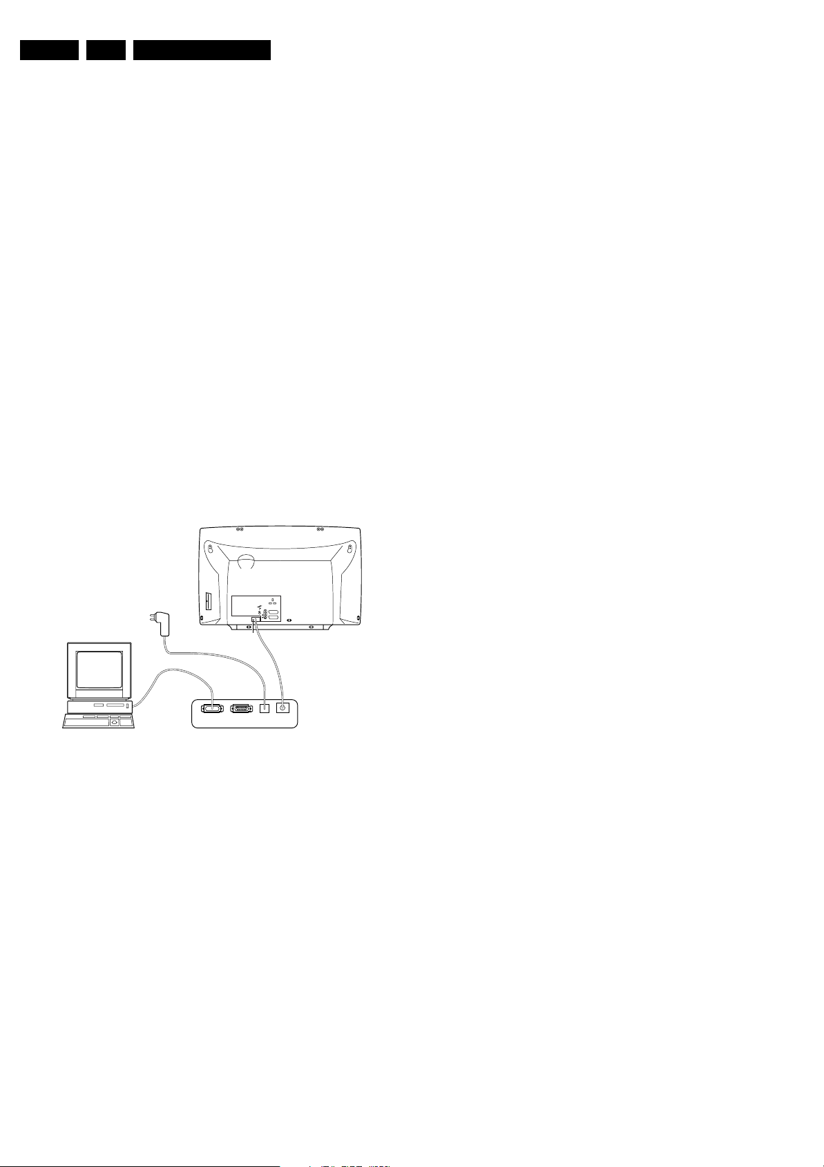
EN 28 FTL13E AA & AB5.
Service Modes, Error Codes, and Fault Finding
Note (*):
• When the set is in stepwise mode and, due to stepping-up,
a protection is activated, the set will really go into protection
(blinking LED). The set will not leave the stepwise-mode
however. If state X is the state where the set went to
protection, stepwise start-up will return to state X-1. At
state (X-1) diagnostic measurements can be performed.
Also, in the short time the set is in state X but not yet in
protection, you can also do some measurements.
5.4.4 How To Connect
1. First, install the ComPair Browser software (see the Quick
Reference Card for installation instructions).
2. Connect the RS232 interface cable between a free serial
(COM) port of your PC and the PC connector (marked with
“PC”) of the ComPair interface.
3. Connect the mains adapter to the supply connector
(marked with “POWER 9V DC”) of the ComPair interface.
4. Switch the ComPair interface “OFF”.
5. Switch the television set “OFF” with the mains switch.
6. Connect the ComPair interface cable between the
connector on the rear side of the ComPair interface
(marked with “I2C”) and the ComPair connector at the rear
side of the TV.
7. Plug the mains adapter in a mains outlet, and switch the
interface “ON”. The green and red LEDs light up together.
The red LED extinguishes after approx. 1 second while the
green LED remains lit.
8. Start the ComPair program and read the “Introduction”
chapter.
5.5 Error Codes
5.5.1 Introduction
The error code buffer contains all detected errors since the last
time the buffer was erased. The buffer is written from left to
right, new errors are logged at the left side, and all other errors
shift one position to the right.
When an error has occurred, the error is added to the list of
errors, provided the list is not full or the error is a protection
error.
When an error occurs and the error buffer is full, then the new
error is not added, and the error buffer stays intact (history is
maintained), except when the error is a protection error.
To prevent that an occasional error stays in the list forever, the
error is removed from the list after 50+ operation hours.
When multiple errors occur (errors occurred within a short time
span), there is a high probability that there is some relation
between them.
5.5.2 How to read the Error Buffer
Use one of the following methods:
• On screen via the SAM (only if you have a picture).
Examples:
– 0 0 0 0 0: No errors detected
– 6 0 0 0 0: Error code 6 is the last and only detected
error
– 9 6 0 0 0: Error code 6 was first detected and error code
9 is the last detected error
• Via the blinking LED procedure (when you have no
picture). See next paragraph.
•Via ComPair.
EXTERNAL 2
L
R
AUDIO EXTERNAL 1
SERVICE
CONNECTOR
PC VCR I2CPower
9V DC
Figure 5-3 ComPair Unit
5.4.5 How To Order
ComPair order codes (EU/AP/LATAM):
• Starter kit ComPair32/SearchMan32 software and
ComPair interface (excl. transformer): 3122 785 90450.
• ComPair interface (excluding transformer): 4822 727
21631.
• Starter kit ComPair32 software (registration version): 3122
785 60040.
• Starter kit SearchMan32 software: 3122 785 60050.
• ComPair32 CD (update): 3122 785 60070 (year 2002,
3122 785 60110 (year 2003).
• SearchMan32 CD (update): 3122 785 60080 (year 2002),
3122 785 60120 (year 2003).
• ComPair interface cable: 3122 785 90004.
• ComPair firmware upgrade IC: 3122 785 90510.
• Transformer Europe: 4822 727 21632.
• Transformer UK: 4822 727 21633.
CL96532156_029.eps
190600
5.5.3 How to clear the Error Buffer
Use one of the following methods:
• By activation of the “RESET ERROR BUFFER” command
in the SAM menu.
• With a normal RC, key in sequence “MUTE” followed by
“062599” and “OK”.
• When you transmit the commands “DIAGNOSE” - “99” “OK” with ComPair (or with a DST).
• If the content of the error buffer has not changed for 50+
hours, it resets automatically.
5.5.4 Error Codes
In case of non-intermittent faults, clear the error buffer before
you begin the repair. This to ensure that old error codes are no
longer present. Before clearing the buffer, write down the
content, as this history can give you significant information.
If possible, check the entire contents of the error buffer. In
some situations, an error code is only the result of another error
code and not the actual cause (e.g., a fault in the protection
detection circuitry can also lead to a protection).
There are various errors:
• I2C device errors.
• I2C bus errors.
• Protection errors.
• Errors not related to an I2C device, but of importance:
– FALCONIC (ERROR 26): at start-up, after initialisation
of the PICNIC, the presence of the FALCONIC can be
checked.
– EAGLE (ERROR 27): at start-up, after initialisation of
the PICNIC, the presence of the Eagle can be
checked.
Note: If you encounter any problems, contact your local
support desk.
Page 29
Service Modes, Error Codes, and Fault Finding
Table 5-2 Table Errors
Error Device Description Def. item Def. Module indication Diagram
1 M24C32 NVM, spontaneous blinking error 1 7011 Control B5a
3 SAA4978 PICNIC 7713 Feature Box B3a
4 Supply 5 V 5V protection / +5V Supply B5a
5 Supply 8 V 8V protection / +8V Supply B5a
6 Slow I2C bus blocked Spontaneous blinking error 6 / Slow I2C Blocked /
8 TDA932x HIP High-end Input Processor 7323 Chroma IF IO B2
13 UV1318/... Tuner protection 1T01 Tuner B13
14 MSPxxxx ITT sound processor 7A02 Audio module B6a
18 Fast I2C bus blocked Spontaneous blinking error 18 / Fast I2C Blocked /
21 M62320P I/O Expander 7P56 Video Dual Screen B15b
26 SAA4992 Falconic 7718 +3V (FBX) Supply B3b
27 T8F24EF Eagle 7724 +3V (FBX) Supply B3c
32 M29W400BT Flash Ram (EPG) 7012 EPG Memory B5a
53 AD9883A AD converter 2fh input 7L01 HD B19c
55 DC/DC converter One of the voltages is not ok + protection error / Supply /
56 EPLD EPLD error 7V01 Video control B19d,f
76 - Audio DC protection - - A
83 TEA6422 Source select matrix audio 7I17 Audio Source Select B14d
EN 29FTL13E AA & AB 5.
Note:
• Error codes 1, 6, or 18 are protection codes and in this
case, supplies of some circuits will be switched “OFF”.
Also, in protection, the LED will blink the number of times
equivalent to the most recent error code.
5.6 The Blinking LED Procedure
5.6.1 Introduction
Via this procedure, you can make the contents of the error
buffer visible via the front LED. This is especially useful for fault
finding, when there is no picture.
When the SDM is entered, the front LED will show (blink) the
contents of the error-buffer. Error-codes > 10 are shown as
follows:
– A long blink of 750 ms (which is an indication of the decimal
digit),
– A pause of 1.5 s,
– “n” short blinks (where “n” = 1 - 9),
– When all the error-codes are displayed, the sequence
finishes with a LED blink of 3 s,
– The sequence starts again.
Example: Error 12 9 6 0 0.
After activation of the SDM, the front LED will show:
– 1 long blink of 750 ms (which is an indication of the decimal
digit) followed by a pause of 1.5 s,
– 2 short blinks followed by a pause of 3 s,
– 9 short blinks followed by a pause of 3 s,
– 6 short blinks followed by a pause of 3 s,
– 1 long blink of 3 s to finish the sequence,
– The sequence starts again.
Note: If errors 1, 6, or 18 occur, the LED always gives the last
occurred error even if the set is NOT in service mode.
5.6.2 How to Enter
Use one of the following methods:
• Enter the SDM (only via soldering pads marked “SDM” on
SSP). The blinking front LED will show the entire contents
of the error buffer (this works in “normal operation” mode
and in “protection” mode).
• Transmit the commands “MUTE” - “062500” - “OK” with a
normal RC. The complete error buffer is shown. Take
notice that it takes some seconds before the blinking LED
starts.
• Transmit the commands “MUTE” - “06250x” - “OK” with a
normal RC (where “x” is a number between 1 and 5). When
x= 1 the last detected error is shown, x= 2 the second last
error, etc.... Take notice that it takes some seconds before
the blinking LED starts.
• “DIAGNOSE X” with the DST (where “x” is a number
between 1 and 5). When x= 1 the last detected error is
shown, x= 2 the second last error, etc.... When x = 0 all
errors are shown.
5.7 Protections
5.7.1 Introduction
This chassis has only one microprocessor (OTC), which
remains active during Standby. This because power of the
microprocessor and the attached memory chip set is coming
from the 3V3 supply, which is derived from the 5V Standbycircuitry. Therefore, in both Power-on as in Standby mode, the
microprocessor is connected to this power supply.
If a fault situation is detected, an error code will be generated
and if necessary, the set is put in protection mode. The
protection mode is indicated by the blinking of the front LED at
a frequency of 3 Hz (or by a coded blinking in special cases).
The content of the error buffer can be read via the service menu
(SAM), the blinking LED procedure or via DST/ComPair.
To get a quick diagnosis, this chassis has three service-modes
implemented:
• The Customer Service Mode (CSM).
• The Service Default Mode (SDM). Start-up of the set in a
predefined way.
• The Service Alignment Mode (SAM). In this mode, items
of the set can be adjusted via a menu.
You can enter both SDM and SAM modes via the “service
pads” on the SSP, via an RC-transmitter (DST or standard RC),
or via ComPair. It is not possible to enter the SAM in “standby”;
the TV has to be in “normal operation” mode.
The “Protection Diagram” shows the structure of the protection
system. See diagram below.
Page 30

EN 30 FTL13E AA & AB5.
Service Modes, Error Codes, and Fault Finding
5.7.4 Hardware Protection
TUNER
FAST I2C BUS BLOCKED
SLOW I2C BUS BLOCKED
EPLD
+
FBX
+
3D COMB (US)
DC_PROT (from audio)
+8V_CON
+5V_CON
DC/DC
PROTECTION
IRQ-DIGITAL (98)
+8V SENSE (105)
+5V SENSE (106)
I2C
Figure 5-4 Protection diagram.
There are several types of protections:
• I2C related protections.
• OTC related protections (via polling on I/O pins or via
algorithms).
• Hardware protection
All protections are explained below.
5.7.2 I2C Related Protections
In normal operation, some registers of the I2C controlled ICs
are refreshed every 200 ms. During this sequence, the I2C
busses and the I2C ICs are checked.
An I2C protection will take place if the SDA and SCL lines are
short-circuited to ground, or to each other. An I2C error will also
occur, if the power supply of the IC is missing.
DC/DC protection: When a 3V3 supply is short-circuited the
DC/DC converter switches off and goes in protection. The
FBX, EPLD IC, and 3D comb IC (US only) have no supply
voltage and give no acknowledge. In this case, the set should
go into protection. An error code is written in the NVM: DC/DC
error.
FBX protection: the FBX protection is not available any more.
It is replaced by the DC/DC protection.
5.7.3 OTC Related Protections
If a protection is detected at an OTC input, the OTC will start to
scan all protection inputs every 200 ms for 5 times. If the
protection on one of the inputs is still active after 1 s, the
microprocessor will put the set in the protection mode. Before
the scanning is started, a so-called “ESD refresh” is carried out.
This is done, because the interrupt on one of the inputs is
possibly caused either by a flash or by ESD. As a flash or ESD
can influence IC settings, the HIP, MSP, 3D Comb (US only)
and wireless module (not used in this set) are initialised again,
to ensure the normal picture and sound conditions of the set.
8 V and 5 V protections: The microprocessor senses the
presence of the 8 V and 5 V (via the “+5V_CON” and
“+8V_CON” lines). If one (or both) of these voltages is (are) not
present, an error code is stored in the error buffer of the NVM,
and the set is put in the protection mode.
Audio DC protection: The OTC senses if the audio module is
in protection via IRQ-DIGITAL (pin 98 of OTC). If this is the
case, the OTC puts the set in protection.
OTC
CL 36532053_065.eps
100703
Short-circuiting the 3V3 supply from the DC/DC converter will
shut down the DC/DC converter. The absence of the 3V3
supply line is also sensed via I2C (see description DC/DC
protection above), this is useful if there is something wrong in
the detection circuit of the DC/DC converter. There are no
hardware protections in this chassis, which switch off the
supply.
5.8 Repair tips
5.8.1 3V3 Supply (DC/DC converter)
As mentioned above, the DC/DC converter is switched “off”
when something goes wrong (detection of a missing 3V3
supply at one of the devices supplied by the 3V3).
Because of this, the set goes to protection (I2C protection).
Error code 55 is logged.
For further diagnoses, you need to overrule the I2C protection:
put the set in Service Default Mode by means of the solder
pads on the SSB.
The DC/DC converter is still not working because it is switched
“off” by the 3V3_FAULT line (schematic B12). Now you have
some possibilities:
1. First, measure the impedance over diode 6U06. In normal
conditions, you should measure approximately 120 ohm (if
possible, verify this with another set). If the impedance is
much too low, do not try to start up the converter as
mentioned below. Remind that if FET 7U03 is shortcircuited, this will also influence your measurement.
2. Desolder coils 5U05 and 5U06, connect an external 3V3
supply at capacitor 2U23 (current limitation to 500 mA) and
a second external 3V3 supply at capacitor 2U31 (current
limitation to 800 mA). The normal working current of the
3V3_SIM line is approximately 400 mA and the normal
working current for the 3V3_DCDCFBX line is
approximately 700 mA. Therefore, if one of the currents
exceeds their nominal value you can determine in which
circuit the overload is situated. If the set would start up and
you have normal picture, there is probably no overload but
a problem in the detection circuits.
3. If you do not have two external power supplies, you can do
the following: Desolder coils 5U02, 5U03, and 5U04 (you
must desolder all three, otherwise the circuit could be
damaged), connect an external power supply of 3V3 at the
cathode of diode 6U06. Make sure to limit the current of this
external supply to approximately 1200 mA. If the supplied
current exceeds 1100 mA (approximately normal working
current) you can conclude that one of the devices supplied
by 3V3 is short-circuited.
4. Another possibility is to force the converter to start up by
short-circuiting (and keep short-circuited) resistor 3U25
(B12).
Caution: Be aware that this can damage the set. Even if
you measure approximately 120 ohm over diode 6U06,
there can still be something wrong in the converter itself.
By short-circuiting resistor 3U25, the internal protection of
the converter is disabled.
5.8.2 ComPair
This chassis does not have an IR transmitting LED (as in MGsets). Therefore, a “Service” (ComPair) connector is
implemented at the rear side of the set, which is directly
accessible (as in A10-, EM2E-, EM3E and EM5E-sets). In
addition to this, there is also a blinking LED procedure to show
the contents of the error buffer.
When you use ComPair, you have the possibility to activate a
“stepwise start-up” mode. With this mode, you can initiate the
start-up sequence step by step. This also means that in certain
Page 31

Service Modes, Error Codes, and Fault Finding
EN 31FTL13E AA & AB 5.
steps, some protections are not activated. This is sometimes
very convenient during repair.
5.8.3 Protections
Activating SDM via the “service pads” will overrule the
processor-controlled protections, but not the hardware
protections. This means, that the A/D-input protections (5 and
8 V) and the I2C “not-acknowledging” info of FBX + EPLD + 3D
Comb (US) and of the tuner are overruled.
Caution: When doing this, the service technician must know
what he is doing, as it could lead to damaging the set.
Table 5-3 Repair tips
Phenomenon Possible Cause Repair tip
No picture, LED blinking at 3 Hz.
No picture, LED blinking with code 6-6-6 or
18-18-18.
No picture, LED blinking with code 1-1-1.
No RC-reception. LED
does not echo RCcommands.
Picture is not synchronised.
Picture is distorted. Check video-path in Serv-
Picture with horizontal
stripes.
No menu, no OSD. Probably a defective uP. Measure test points B61to B64 on diagram B5A.
No NextView (EPG). IC7012 defective or not
No Teletext. IC7007 defective or not
Problems caused by
EPG (Electronic Program Guide). The TV
set "hangs".
NexTView EPG is not
functioning only Teletext guide.
Various symptoms,
due to missing local
supply voltage.
For ITV (Institutional
TV) models, it is possible that the service
modes are not functioning as expected.
Set is in protection due to
various causes. For error
codes see error-code list.
No communication on slow
I2C- or fast I2C-bus.
No communication on
NVM-I2C bus to the uP.
uP circuitry or RC-receiver
is defective.
The sync is derived in the
HIP.
ice Default Mode.
Pixel Plus processing is
malfunctioning
powered.
powered.
Problems with NexTView
EPG broadcasts.
EPG version 2C3 is
switched off during production.
An interrupted fuse, NFRresistor or connection.
"Hotel Mode" option is set
to "ON". This can cause
problems with service
modes.
5.8.4 Power Supply
The simplest way to repair the power supply is to check (and
replace if necessary) the components that are marked grey on
schematic SP1.
5.8.5 AUX Supply
First, determine whether one or more of the secondary diodes
(6044, 6021, 6291, 6293) are short-circuited. If this is not the
case, check (and replace if necessary) the components that
are marked grey on schematic SA.
You have no picture, so:
- Read the error buffer via ComPair (error buffer is accessible when set is in
protec tion, compare-file will guide you to this)
- Read the blinking LED information via standard remote command
<mute>06250x<ok>.
- Or you read the error code sequence via standard remote command
<mute>062500<ok>.
When you have found the error, check the circuitry related to the supply voltage and
I2C-communication or the circuitry that triggers the protection.
As processor cannot communicate with one of the 2 busses it the standby-led spontaneously starts blinking 6-6-6-etc or 18-18-18-etc...
If in the error buffer somewhere is an error 6 or 18, these will have the highest priority
starting the mentioned blinking.
Measure dependent of the error on the I2C-bus which device is loading the bus. (Use
I2C-overview)
As the uP cannot communicate with the NVM I2C bus, it spontaneously starts blinking
1-1-1.
Note: when there is no access to the NVM, a lot of picture setting can go wrong.
In case the set does react on a local keyboard operation, you must check the RC-receiver circuitry (diagram LD).
Check crystals in the HIP circuit on bad contacts.
Investigate whether there is an error code present in the error buffer. In case there is
one, check the I2C-bus and/or supply lines (see overview supply lines).Measure and
check signal path Tuner-HIP-FBX-EPLD.
Check functionality on circuitry (B3a, B3b, and B3c) of PICNIC (7713), FALCONIC
(7718, EAGLE (7724) and/or field memories (7714, 7717, 7719, 7722 and 7723.
Tip: the whole Pixel Plus chipset (3 ICs + 5 Field Memories) can be diagnosed via
ComPair.
Check circuitry around IC7012 on diagram B5A.
Check circuitry around IC7007 on diagram B5A. Check also B61 to B64 around uP on
diagram B5A.
To switch from EPG 2C3 to Teletext guide. Press for 4 seconds, simultaneously the
Menu button on the TV and digit 0 on the remote. The option settings for NexTView
type and Flashram will not change.
To switch from Teletext guide to EPG 2C3. Press for 4 seconds, simultaneously the
Menu button on the TV and digit 1 on the remote. The option settings for NexTView
type and Flashram will not change.
When no symptom or error code leads you to a specific circuitry, use the supply lines
overview (see supply lines overview), for a quick scan of all supply lines.
Switch "OFF" the "Hotel Mode" option, in "Service Alignment Mode", "Service Options", "Miscellaneous", "Hotel Mode". After repair this option should be switched on
again to use Hotel Mode functionality.
Page 32

EN 32 FTL13E AA & AB5.
5.9 Software Downloading
In this chassis, you can upgrade the software via ComPair
without removing the back cover of the set. The switch, which
is needed for the software downloading procedure, can be
reached through the cooling gaps of the back cover. The switch
is located next to the SAM/SDM pads and can be operated with
a long and thin screwdriver. Make sure that you do not damage
the PWB with sharp objects. You can find more information on
how this procedure works in the ComPair file. It is possible that
not all sets are equipped with the hardware, needed to make
software upgrading possible. To speed up the programming
process the firmware of the ComPair interface can be
upgraded. See paragraph “How To Order” for the order number
Service Modes, Error Codes, and Fault Finding
Page 33

Wiring Diagram, Block Diagrams and Overviews
6. Wiring Diagram, Block Diagrams and Overviews
Wiring Diagram
33FTL13E AA & AB 6.
LSP
HIGH
R
Backlight
Supply
Connector
LCD Panel
16P
0304 0303
4P 4P
Audio
A
Amplifier
Class D
amplifier
8P
9P
0388
0302
LCD Panel
1Y45
3P
5P
9P
1302
16P
1313
1I70
1312
16P
1345
20P
nn
1Y01
3P
LVDS
Connector
20P
P
5P
1370
Topcontrol
SA
9P
1355
1Y55
9P
Aux Supply
5P 7P
1346
nn
1333
2P
10P
1S20
1309
2P
1309
SP
LCD PanelLCD Panel
LSP
HIGH
L
Power Supply
LD
6P
0317
LSP
R
LOW
LSP
R
LOW
Mains
switch
10P
Backlight
Connector
11P
0320
ONLY FOR ITV MODEL
O
Side I/O
Supply
0936
16P
CN1CN1
6P
1903
B
SSP
8P
5P
11P
7P
1333
1S88
LSP
L
LOW
LSP
L
LOW
1S361S46
2P
1308
MAINS
CL 36532053_049.eps
291003
Page 34

Wiring Diagram, Block Diagrams and Overviews
Block Diagram Supply and Supply Lines
RECTIFIER / DOUBLER
SP2
6807
GBJ6J
7805 (str83145)
7801 - 7803
POWER SUPPLY
SP1
0308
2
1
3507
+
-
VOLTAGE
DOUBLER
(for 110V only)
1400
T3.15AH
6506
DF06M
-
CONTROL
7500
TNY266
4
ENABLE
400V-HOT
5401
5403
MAINS
FILTER
+
DRAIN
SOURCE
TCET1102
5
7-8
7501
1309
1
2
5500
2
3
4
3
HOT COLD
AUX SUPPLY
SA
1309
1
3
7017
7018
CURRENT
PROTECTION
1450
23
14
7460
7505
CONTROL
6
7
8
9
3501
1
7502
TL431
2
5003
2001
SOFT
START
+
RELAY
6515 6516
6505
+5V-SW
1
2
3028
3031
3032
3007
2510
2510
3
STANDBY
V TUN
+5V-SW
+5V2
+5V2-RELAY-IO2
2x
POR
7001
MC34067P
11
OSCC
7
ERROR
11
SOST
7003
7004
PROTECTION
3505
3503
BIAS SUPPLY
15
VCC
CONTROL
VOLTAGE
OVER
HOT COLD
14
OA
12
OB
10
FI
STANDBY SUPPLY
7503
7504
POR
CIRCUIT
6504
7531
STD16NEO6L
D
7506
7507
7532
SWITCH
6503
CONTROL
1333
1
2
3
4
5
6
7
34FTL13E AA & AB 6.
SUPPLY & DC PROTECTION
COLDHOT
5002
3057
1
2
6044
STPS20L40CFP
1005
3
9
T5A
10
1006
11
1
T5A
12
13
14
15
16
5025
5026
6021
STTH2003C
1
3
3030
+12V
2
3022
3052
+24V
2
7210
TL431CZ
3024
VS Voltage
Adj.
3026
4
7003
PCET1102
3
3000
5001
10
11
4
2
14
13
7008,
7021, 7022
7007
7020
HIGH
SIDE
DRIVE
LOW
SIDE
DRIVE
60786079
2003
STU16NB501
G
7006
STU16NB501
G
7005
S
8
7
D
S
5040
3
5
D
HOT
COLD
1007
AUDIO SUPPLYVS SUPPLY
6293
7011
L4940
6291
OUT
VSND-NEG
VSND-POS
+5V2
DC-PROT
DC-PROT
+5V2
+12V
+8V6
+24V
T5A
IN
B20
1355
1Y55
BACKLIGHT-CTRL
2x
POR
LIGHT-ON
2x
FAN-SPEED
STANDBY
V TUN
+5V-SW
+5V2
POR
STANDBY
1x
DC-PROT
+5V2-RELAY-IO2
1x
+5V2
V TUN
+12V
+5V2
+8V6
+12V
-5V-SW
1x
1x
3x
1x
+5V2-RELAY-IO2
POR
V TUN
+5V2
S
G
1333
1
2
3
4
5
6
7
+5V-SW
+5V2-RELAY-IO2
STANDBY
+5V2-RELAY-IO2
N.C.
TEMPERATURE
SWITCH PANEL
LD
+8V6
+5V-STBY-SW
1101
1
2
3
SENSOR
+9V-STBY-SW
+9V-STBY
ON
5100
4
5
ON / OFF
6
SWITCH
T+
3072
1370
1346
0320
10
1
2
3
4
5
6
7
8
9
1
2
3
4
5
1
2
3
4
5
BACKLIGHT-CTRL
1
2
3
4
FAN-SPEED
5
STBY-TEMP
6
STANDBY-IO2
7
DC-PROT-IO2
8
+5V2-RELAY-IO2
9
POR-IO2
LAMP-ON
B5B
B1
B19F
N.C.
N.C..
B1
B5A
B14A
1I70
1
2
3
4
+5V2
5
+5V2
B1
1S46
1
2
+8V
3
+11V
4
+5V
5
1S20
6
8
9
5S03
6
8
9
5S08
10
+5V2
+33V
+11V
3IK7
5S02
+8V-AUD
5S01
+8V-VDP
5S04
+5V-CON
5S05
+5V-VDP
5S03
+5V-AUD
+5V2-RELAY-IO2
+5V2
+8V
+8VA
+8V
+5V
+8V
A7
0323
0323
1
1
2
2
3
3
4
4
5
5
6
6
7
7
8
8
9
9
1x
2x
1x
2x
1x
2x
1x
1x
3x
1x
2x
4x
1x
7x
3x
2x
1x
1x
5725
5335
DC-PROT
B12
CONTROL
+11V
B2
+5V2-RELAY-IO2
+5V2_CON
+8V
+8V_CON
+5V_VDP
+8V_VDP
B4
+8V_VDP
+5V_VDP
B5A
+8V_CON
+5V2_CON
+5V_CON
B6A
+5V_AUD
+8V_AUD
+5V
+5VF
+11V_S
B5B
+5V_CON
B13
+5V
+33V
B14C
+5V
B14D
+5V
+8V
1740
7745, 7746
2A5
STAB
1730
7735, 7736
2A5
STAB
DC/DC CONVERTER
+11V
1U01
T800mA
7U04
G
7U03
G
+3V3_FAULT (x lines)
IF / IO
1403
5415
F500mA
5416
3402
3400
HOP
3329
3304
OTC
7005
OUT
IN
AUDIO DEMODULATOR
5A00
5A03
3A03
+5V
5A06
5A01
BACKLIGHT CONTROL
TUNER
2FH I/O
3IN4
AUDIO I/O
5U02
D
S
D
S
VSDN-NEG
Vcc-10-NEG
VSDN-POS
Vcc-10-POS
+9V-STBY
5U01
+5V2_CON
+8V_CON
+5VCOM
+8VP
+8V_VDP
+5VS
+8V_VDP
+8VS
+5V_VDP
+5VS
+8V_CON
+5V2_CON
+3V3_INTOTC
+5V_CON
+5DA
+5DB
+8V-AUD
+8VC
+5VF
+11V_AUD
+5V_CON
+5V
+33V
+5VIO
+5V
+8V
6U02
5U05
5U06
+8Vp
9,19,20,
38,49,
75,101,
SAA5801H
A2
5404
11
7323
TDA9320H
HIP
+5VCOM
7307
TDA9181
111
7001
OTC
104
31
7A02
MSP3
AUDIO
PROC.
FILTERS
Vcc-10-NEG
Vcc-10-POS
+9V-STBY
+3V3_LINK
N.C.
+3V3_SIM
+3V3_DCDC FBX
+3V3_DCDC FBX
5405
45
6.5
B5B
B5C
+3V3_INTOTC
B1
STANDBY-IO2
A3 A6
+3V3_SIM
+5V-CON
OTC-FLASH
:
VSDN-NEG
Vcc-10-NEG
VSDN-POS
Vcc-10-POS
+5V2
+5V
+11V
+8V
1x
B15B
1x
+5V
B19F
+3V3-EPLD
B19A
+8V
B19C
+5V
+3V3-I2C
1x
1x
B19D
1x
+3V3-SIM
+3V3-EPLD
2x
+3V3-I2C
B19E
+5V
I/O EUR
B14B
3IC1
+5V
3IB4
7I09
3IB5
PIP IF I/O
B15A
3P02
5P01
I/O
5P51
EPLD
3D73
5D51
3D81
6D93 6D64
HD1 A/D CONVERTER
7L02
5L07
5L13
5L09
5L14
5L11
5L15
EPLD CONTROL
5E53
7E05
3
1
3E08
5E08
3E10
5E07
3E14
3E18
3E09
5E06
3E13
3E17
9E59
5E51
5E50
7I07
+24V
LIGHT-ON
BACKLIGHT
CTRL
+24V
LIGHT-ON
BACKLIGHT
CTRL
+5V2
+5V
+11V
+11V_S
+11V_S
+8VIPP
+5VD
+3V3-EPLD
+8-VIDEO
REF1
6D62
REF2
REF3
+3V3-I2C
VD
VD-1
VDD
VDD-1
PVD
PVD-1
+3V3-EPLD
+3V3-AD
+3V3-IO
+1V5
+1V5-PLA
+3V3-I2C
+5VA-OSD
+VB
3
7E18
4
+VT
3
7E15
4
B20
1x
+11V
+3V3-EPLD
LCD-PWR-ON
B3A
+5VF
+5VA
1x
+3V3
_DCDC FBX
+2V5B
2x
+3V3_FBX
2x
1x
+3V3A
+3V3_INT
1x
B3B
+3V3_FBX
+2V5B
+3V3_INT
B3C
+3V3_FBX
+5VA +5VA
+2V5B
+3V3A
+8V_CON
7Y00
IRFR9024N
3
1
7109
PICNIC
5756
5744
5747
5746
FALCONIC
5719
5718
5753
5716
5717
EAGLE
+5VA
5748
5721
+3V3A
+8V_CON
+12V-LCD
2
+3V3_INT
To 7717
To 7719
3Y03
3Y04
5706
+3V3_FBX
+3V3_FBX
+3V3FA
+3V3_FAULT
+2V5FB
+3V3_FAULT
+3V3_FAULT
5725
5722
1Y01
3
4
5
6
B12
B12
B12
+2V5_E
+2V5FCA
+2V5FCD
5742
LCD
DISPLAY
1312
1-6
12
13
14
1313
1-6
12
13
14
7706
5714
5729
5731
5737
5713
5745
7726
5738
5724
5727
5726
7727
5743
5728
CL 36532053_059.eps
BACKLIGHT
CONNECTOR
BACKLIGHT
CONNECTOR
LVD S
CONNECTOR
+5VA
+2V5B
11-7713
5736
+3V3A
+3V3_INT
+3V3FM
+3V3P
+3V3FCD
+3V3FC1
+3V3FC2
+1V5_E
+1V5FCA
+1V5FCC
291204
24-7713
+3V3_E
Page 35

Wiring Diagram, Block Diagrams and Overviews
35FTL13E AA & AB 6.
Testpoint Overview Aux Supply and Power Supply
SA AUX SUPPLY (TRACK SIDE VIEW) SP POWER SUPPLY (TRACK SIDE VIEW)
19
1312
1
1355
1370
5
1
7011
OUT
G
IN
6021
3
2
6293
6044
2
1
3
1
A
K
+24V
1313
1
1
+12V
VS
+
Adj
3026
1346
1333
7
1
5
1
7005
S
D
G
5
5001
DRIVER
1
10
6
5002
MAINS
TRAFO
116
89
400V_HOT
7006
D
1309
2
1
S
G
6807
1309
400V_HOT
1
2
HOT
COLD
9
1302
6291
169
A
K
COLD
HOT
7001
CONTROL
18
+
7500
CONTROL
41
5
58
1
6
5500
9
7531
SG
D
+5V_SW
1333
1
7
1400
FUSE
0308
12
MAINS INPUT
COLD
HOT
CL 36532053_069.eps
180703
Page 36

Block Diagram Video
VIDEO
TUN1
B13
1
2
3
4
5
6
7
8
9
10
CVBS-TER-OUT
+33V
+33V+5V
5T02
6TO8
1TO1
UV1318ST
TUNER
-/33
7,3
9
11
1
ERR
13
15
4
AGC1
S-SDA
S-SCL
CVBS-SC1-AV1-IN
CVBS-AV3-IN
Y-CVBS-SC2-AV2-IN
C-SC2-SVHS-IN
Y-CVBS-FRONT-IN
C-FRONT-IN
CVBS-SC2-MON-OUT
R/G/B-SC1-Y/U/V-IN
R/G/B-SC2-IN R/G/B-SC2-V-IN
B2
T1
IF-TER
AGC
MONITOR
B5A
Wiring Diagram, Block Diagrams and Overviews
IF, I/O VIDEOPROCESSING
7402
5403
40,4
SAW FILTER
AUDIO
1409
SAW FILTER
VIDEO
1410
1408
TUNER AGC
7411
I5
VIF1
VIF2
62
64
SIF2
63
SIF1
SOUND-OUTPUT
EF
7323
TDA9320H
2
3
7410
PLL
DEM
QSS
MIXER
DEMO
AM
1407
SOUND
FILTER
I6
V1
10 12 13 14
GROUP
DELAY
COR.
QSS-AM
5
QSS-AM
B6A
7322
HIP
SEE
BLOCK DIAGRAM
AUDIO
7415
CVBS-TXT
B5A
OTC
7307
7320
EF
V2
ERR
8
TDA9181
EF
12
Y5
26 29
VIDEO
SWITCH
+
CONTROL
16
18
20
21
23
24
COMB
FILTER
CY
32
34
N.C.
Y
C
28
PROC.
PROC.
SYNC
SEPAR.
14 Y
16
C
Y
C
R
SCART1
36 37 38 39
7412
G B
EF
Y
Y/U/V
U
SWITCH
V
UU
VY V
DECODER
PAL
NTSC
SECAM
H-SYNC
PROC.
V-SYNC
PROC.
UY
V
RGB/YUV
MATRIX
R G B
41 42 43 40
36FTL13E AA & AB 6.
TUN1
B6A
7414
V6
9A04
49
50
51
60
61
54
57
46
47
SCART2
Y50
U50
V7
V50
V8
L8
HA50
F14
VA50
1305
PAL
4.43MHz
1308
NTSC M
3.57MHz
SCL-F
SDA-F
Y-PIP+MAIN-OUT
9A05
U-PIP+MAIN-OUT
9A06
V-PIP+MAIN-OUT
HA50
7740
24
1
7741
24
1
VREF
VA
23145
SWITCH_2FH
SWITCH_1FH
B3A
3727
3722
PICNIC
L6
L7
L8
L10
L11
SCL-F
SDA-F
INTR1
B3B
7711
64K
M27C512
PROM
7712
74HC573D
LATCH
7713
SAA4978H
23
25
26
28
29
4
5
DIGITAL
3x
SIGNAL PROCESSING
ADC
PICNIC FALCONIC
ERR
3
SYNC PROCESSING
DA (0-15)
CLI6
WEC
RSTW
RSTR
1
2
30
89
SNDA
SNCL
Href-EXT
CLK 32P
12,21
7714
MS81V04160
FIELD
MEMORY
FM1
RNRST
REF
21
12
13(2x)
SNDA
SNCL
MF (1-17)
FEA
FALCONIC
7718
SAA4992
7717
MSM54V12222A
FIELD
MEMORY
2
ERR
26
7717
MSM54V12222A
FIELD
MEMORY
3
B3C
Y-2FH (0-7)
UV-2FH (0-7)
YF (0-7)
UVF (0-7)
EAGLE
Y-2FH (0-7)
UV-2FH (0-7)
B3D
7743
7745
7742
7744
BUFFER
BUFFER
BUFFER
BUFFER
BUFFERS
YF-BUFF (0-7)
UVF-BUFF (0-7)
2,5,11,18,
19,20,23
7722
MS81V04160
FIELD
MEMORY
FM4
(lower lines)
7723
MS81V04160
FIELD
MEMORY
FM5
(lower lines)
18
19
20
2
5
11
23
YGO (0-7)
UVGO (0-7)
YGO (0-7)
HVGO (0-7)
CLK32I
FALREF
REFIN
Vref
INSTR1
SNDA
SNCL
Href
CLK32E
7724
TBF24EF
EAGLE
ERR
27
Y-OUT (0-9)
U-VOUT (0-9)
RSTR
CLK64
HD-E
VD-E
CLOCK 32O
17
16
14
15
22
B14B
3
1
9
4
8
5
10
7
AV3-CVBS-IN
TER-CVBS-OUT
IN-Y-CVBS-SC2-AV2
SC2-CVBS MON-OUT
SC2-R C-IN AV2
SC2-G-IN
SC2-B-IN-C-OUT
SC2-FBL-IN
SIDE I/O
O B1 B14A
C/16:9
Y
34
SVHS
251
CVBS
VGA RGB
B19A
1
2
3
4
VGA1 IN
5
15P "D"SHELL
CONNECTOR
6
7
10
15
5
8
9
10
1
6
11
11
12
13
14
15
2FH I/O
B14C
R-SC1-IN V-IN
G-SC1-IN Y-IN
B-SC1-IN
IN-SC1-FBL
R-VGA
G-VGA
B-VGA
+5VdcOUT
Y-2
Pb-2
Pr-2
U-IN
SDA
SCL
H-SYNC-VGA
V-SYNC-VGA
SCART 1
21
19
15
11
7
SCART 2
21
19
15
11
7
7D52
7D53
7D54
7D59
M24801
8
5
6
YPbPr/
MATRIX
20
16
8
20
16
8
NVM
YUV
SC1-CVBS
IN-SC1-FBL
STATUS SC1
IN-Y-CVBS-SC2-AV2
P50
STATUS SC2
1936
2
Y
4
C
7
R-VGA-BUF
G-VGA-BUF
B-VGA-BUF
SUB-Y-2FH
SUB-U-2FH
SUB-V-2FH
B2
HIP
B5A
B2
1936
RGB/
YUV/
MATRIX
OTC
HIP
2 Y-CVBS-FRONT-IN
C-FRONT-IN
4
7
Y-V G A
U-VGA
V-VGA
SCART 3
21
19
15
11
7
SCART 4
21
19
15
7
20
16
8
20
16
10
8
AV3-CVBS-IN
STATUS-SC3
B5A
SC1-CVBS
SC4-CVBS-AV3-Y-SVHS
STATUS-SC4
B5A
9I00
9I02
I/O EPLD + LVDS
B15B B19D
7P56
M62320
9
I/O
EXP
S-SDA
3
7138
2
7132
74HC4053
3
5
1
2
13
12
SC2-B-IN-C-OUT
10
11
12
SWITCH-HEF
13
B19D
4
15
14
11
CVBS-SC1-AV1-IN
7E02
EPCS1
EPLD
FLASH
RAM
1E03
PROGRAM
CONN.
2
6
12
14
15
2
6
S-SCL
OTC
B14C
OTC
Y-CVBS-FRONTS-IN
C-FRONTS-IN
9
6
7
8
1
2,3,4,13,16,17,
19,20,21,212,23
9, 10
CLK-2FH
CLK-32P
H-2FH-AD-OUT
V-2FH-AD-OUT
SYNCDET
VA
Href-EXT
HD-E
VD-E
DATA
CLOCK
7V01
EP1C12Q240C0
SWITCH
STANDARD
DEFLECTION
CONTROL
CONTROL
18
22
+
CLOCK
SYNC
INPUT
313
B19F
SUPPLY
CLK-32I
VD-OTC
HD3-OTC
PWR-OK-PDP
LCD-PWR-ON
LAMP-ON
SELECT-VGA-YPBPR
Vref
Href
RSTR
REF
FALREF
REFIN
SWITCH-1FH
SWITCH-2FH
2,3,4,9,10,11,
16,17,18,19,20,21
Y-2FH (0-7)
CLK-2FH
9
CLK-64
16
18(2x)
CLK-VID
25
10
2(2x)
SDA-F3
11
17
SCL-F3
21
SN-CL
19
20
SN-DA
4
3(2x)
25
CLKP
1:2
CLK-OSD
23
24
EPLD
ERR
56
UV
CONVERTION
U-AD (0-7)
UV-AD (0-7)
UV-2FH (0-7)
Y-AD (0-7)
PATH
FOR
3FH
ONLY
Y-OUT (0-9)
UV DEMUX
CONTRAST
SATURATION
BRIGHTNESS
U-VOUT (0-9)
YUV
RGB
CLKP
R-OSD (0-5)
OSD
INSERTION
G-OSD (0-5)
B-OSD (0-5)
to
OSD
ZERO DELAY BUFFER OTC
B19C B5A B3A B19E
7L01
AD9883AKST
SERIAL
57
U-2FH
Y-2FH
V-2FH
56
30
31
49
REGISTER
+
POWER
MAN.
SYNC
PROC.
+
CLOCK
GENERATOR
ERR
53
A/D
COVERTER
66
H-2FH-AD-OUT
64
V-2FH-AD-OUT
65
SYNCDET
67
CLK-2FH
2-9
Y-AD (0-7)
70-77
UV-AD (0-7)
12-19
U-AD (0-7)
SELECT-VGA-YPBPR
6
7
8
9(2x)
10
H-SYNC-VGA
V-SYNC-VGA
SUB-Y-2FH
U-VGA
SUB-U-2FH
Y-V G A
SUB-Y-2FH
V-VGA
SUB-V-2FH
2
6
3
7
4
8
15
16
7D51
TDA8601T
OUTPUT SELECTION
CLAMP
CLAMP
CLAMP
CLAMP
CLAMP
CLAMP
3503
RGB/YPbPr
SDA-F3
SCL-F3
12
3-STATE
11
3-STATE
10
3-STATE
13
3-STATE
5
B3D
SWITCH-2FH
CLK-32I
CLK-32O
7747
2
4
1
7748
24
1
13
3
18
22
2
1
7746
CY23S02
IN
FBIN
8
CLK-32ECLK-32P
OUT
38483855
7001
SAA5801H
77 R-TXT 2FHR-GFX R-OSD
78 G-TXT 2FHG-GFX G-OSD
TXT
79 B-TXT 2FHB-GFX B-OSD
OSD
80 FB-TXT 2FHFB-GFX BL-OSD
SEE ALSO
BLOCK
DIAGRAM
CONTROL
3046-a
3046-b 3706
3046-c 3707
3046-d 3708
BL-OSD (0-4)
3705
R (0-7)
G (0-7)
B (0-7)
45 25
PARITY
55 27
HS-OUT
54 28
VS-OUT
49 30
DE-OUT
50 31
CLK-OUT
53 32
LVDS-PWR-DOWN
+3V3-EPLD
7V02
DS90C385MTD
25 24
HD3-OTC
7E23
7E08
7E13
7E17
7E20
TTL
PARALLEL
to
LVDS
LVDS
transmitter
PLL
1
48
47
46
45
42
41
38
37
40
39
+VB
7E21
CL 36532053_050.eps
B20F
TXLCD0-
TXLCD0+
TXLCD1-
TXLCD1+
TXLCD2-
TXLCD2+
TXLCD3-
TXLCD3+
TXCLKLCD-
TXCLKLCD+
+12V-LCD
CLK-OSD
7E16
AD9066JR
11
6
7E09
AD9066JR
11
6
A/D
A/D
DXB
DXA
1
DXB
DXA
1
180703
1Y01
18
17
16
15
14
13
10
9
12
11
??
??
R-OSD (0-5)
G-OSD (0-5)
B-OSD (0-5)
BL-OSD (0-5)
LCD-
DISPLAY
Page 37

Wiring Diagram, Block Diagrams and Overviews
Testpoint Overview Small Signal Board
SSB side A SSB side B
37FTL13E AA & AB 6.
7001
PIN TP
5 B60
16 B55
83 B57
84 B58
85 B52
86 B51
87 B54
88 B53
7323
PIN TP
2I5
10 I6
12 V1
14 V2
26 V5
46 V10
47 V9
49 V6
50 V7
51 V8
60 L8
61 F14
15P
MIN "D" SHELL
1107
6X CINCH
1101
2X SCART
1104
2X SCART
7L02
7005
7006
FLASH
RAM
7018
OTC
2X
FLASH BUFFER
1408
A/D CONVERTOR
(2FH)
7L01
7746
CLOCK
7019
7323
HIP
OTC
7001
7723
FM4
EPLD
7V01
7719
FM3
7744 7742
2X
BUFFER
7727
7V02
LVDS
TRANSMITTER
7717
FM2
AUDIO
7A00
7A03
7E09
DEM.
7A02
A/D CONVERTOR
(FOR OSD)
A/D CONVERTOR
7E16
(FOR OSD)
7706
7711
PICNIC
PROM
7E02
FLASH
EPLD
RAM
1U06
1U05
1E02
1E03
5U01
7U03
7U04
(SIGNAL CONN.)
1170
7Y00
1Y45
TO LCD
1Y01
7A02
PIN TP
20 B66
21 B67
50 B65
7A03
PIN TP
1 B69
7 B68
7713
PIN TP
23 L6
25 L7
26 L8
28 L10
29 L11
34 L9
7712
LATCH
FM1
7714
PICNIC
7713
1A00
FALCONIC
7718
7743
BUFFER
7A07
7745
7011
NVM
(OTC)
FM4
7722
7012
FLASH
RAM
EPG
FILTER
7307
COMB
EAGLE
7724
7007
DRAM
TXT
1409
7D57
7D51
7D59
7132
SC1/SC4 AUDIO INPUT
-SWITCH
CONNECTOR
B51
2V / div DC
100us / div
L10
1V / div DC
20us / div
COMPAIR
PM3394B
1119
B52
PM3394B
2V / div DC
100us / div
T1
200mV / div AC
10µs / div
7117
1T01
B53
2V / div DC
5ms / div
V1
1V / div DC
10us / div
AUDIO
INPUT
SWITCH
PM3394B
PM3394B
TUNER
T1
B54
2V / div DC
5ms / div
V2
1V / div DC
10us / div
PM3394B
PM3394B
1S36 1S46
B55
PM3394B
2V / div DC
250ns / div
V5
PM3394B
1V / div DC
10us / div
B57
PM3394B
500mV / div AC
10us / div
V6
PM3394B
500mV / div DC
20us / div
1S88 1S20
B58
PM3394B
1V / div DC
5ms / div
V7
PM3394B
500mV / div DC
20us / div
3104 303 3857.3
PM3394B
PM3394B
B65
200mV / div AC
V9
B60
500mV / div DC
10us / div
V8
1V / div DC
20us / div
1Y55
10µs / div
PM3394B
2V / div DC
200us / div
B66
20mV / div AC
1ms / div
V10
PM3394B
2V / div DC
200us / div
B67
20mV / div AC
1ms / div
1U05
5 V / div DC
5µs / div
3104 303 3857.3
B68
20mV / div AC
1ms / div
1U06
5 V / div DC
5µs / div
B69
20mV / div AC
1ms / div
F14
1V / div DC
5ms / div
I5
20mV / div AC
10µs / div
I6
1V / div DC
10us / div
PM3394B
7P56
I/O EXP.
L6
PM3394B
500mV / div DC
10us / div
7120
REG.
SWITCH
L7
PM3394B
500mV / div DC
10us / div
7107
L8
1V / div DC
20us / div
L9
PM3394B
1V / div DC
250ns / div
CL 36532053_068.eps
180703
Page 38

Wiring Diagram, Block Diagrams and Overviews
Block Diagram Audio and Control
BLOCK DIAGRAM AUDIO
SEE ALSO
IF
BLOCK DIAGRAM
B2
VIDEO
7323
TDA9320H
3380
SOUND-OUTPUT
5
HIP
MAIN
SIDE I/O
O
L
R
B14B
L
R
B1
1936
1S36
??
6
8
??
SCART 1
I/O
6
3
2
1
SCART 2
6
3
2
1
SCART 3
6
3
2
1
SCART 4
6
3
2
1
B14C
BLOCK DIAGRAM CONTROLS
BLOCK DIAGRAM CONTROLS
TOP CONTROL
P
5x
CHANNEL +
CHANNEL-
VOLUME+
VOLUME-
O LD
O
KEYBOARD
AND
SIDE I/O
0345
22
PANEL
FOR STANDARD MODEL
L-FRONT-IN
R-FRONT-IN
AL-SC1-IN
AR-SC1-IN
AL-SC2-IN
AR-SC2-IN
AL-SC3-IN
AR-SC3-IN
AL-SC4-IN
AR-SC4-IN
SND-CENTER-IN
(option)
2FH1-L
2FH1-R
B20
1Y45
FRONT
DETECT
7410
KEYBOARD
NOT FOR ITV MODEL
LED PANEL
LD
ON/OFF
SWITCH
7107
RECEIVER
6127
6103
2
1
4
RC
7120
2
1101
4
5
6
GREEN
RED
7103
7105
LIGHT-SENSOR-IN
+5V-STBY-SW
GREEN-LED
RED-LED
RC-IN
+8V6
+9V-STBY-SW
+9V-STBY
3
7
1
2
3
QSS_AM
N.C.
B14D
1
2
3
4
5
6
7
8
9
10
12
11
1936
7
0320
1
2
3
4
5
6
7
8
9
10
AUDIO I/O
4
6
8
10
2
11
3
5
7
9
1
12
1S36
7
OR
OR
IS20
10
B1
7I17
TEA6422D
25
R1
24
R2
MATRIX
SWITCH
23
R3
20
R4
19
R5
18
R6
4
L1
ERR
83
5
L2
6
L3
9
L4
10
L5
11
L6
CONN.
1
N.C.
LED GREEN
2
3
RC
4
LIGHT_SENSOR
5
5S06
6
7
8
+5V-RELAY-IO2
9
5S07
5S08
38FTL13E AA & AB 6.
B6A
13
R1
15
R2
17
R3
12
L1
14
L2
16
L3
SND R-MAIN-IN
SNDL-MAIN-IN
7A02
MSP4450 (used in combination with MAS3528E and DPL4519G)
B65
IF1
50
IF2
2A39
47
45
44
42
SC1
41
39
SC3
38
36
SC4
35
I2S-MSP-OUT
I2S-MSP-WS
N.C.
I2S-MSP-CLK
ADC
MONO-IN
5
4
3
SCART
INPUT
SELECT
DE-
MODULATOR
DSP
ERR
14
ADC
PRESCALE
PRE-PROCESSING
PRESCALE
SOURCE
SELECT
I2S
INTERFACE
LOUD-
SPEAKER
SOUND
PROCESSING
HEADPHONE/
SURROUND
SOUND
PROCESSING
DAC
DAC
DAC
DAC
SCART
OUTPUT
SELECT
7A03
B68
B66
LM833D
20
7
AUDIO-R
21
23
17
18
18
18
5
3
B67
3
HPN-R
HPN-L
MSP-CENTER
MSP-SURR
1
AUDIO-L
B69
7A00
1
AUDIO-SW
N.C.
N.C.
N.C.
LOUD
DACM-SUB
FRONT-DECT
B14D
REG-SW
SNDR-MON-OUT
SNDL-MON-OUT
2IA2
2F99
2
1
5
3
9.10
SNDR-SC1-OUT
SNDL-SC1-OUT
7I20
7I22-B
SNDR-SC2-OUT
15
SNDL-SC2-OUT
4
28
SNDR-SC1-OUT-DC
SNDL-SC1-OUT-DC
29
SNDR-MON-OUT
25
SC
12
I2S-DPL-OUT
15
I2S-DPL-CLK
14
I2S-DPL-WS
SNDL-MON-OUT
26
61
N.C.
HPN-R
HPN-L
B5A
SP1
OTC
B1
SOUNDENABLE
POR-IO2
SA
B14B
SNDL-SC1-OUT
SNDR-SC1-OUT
SNDL-SC2-OUT
SNDR-SC2-OUT
SNDR-MON-OUT
SNDL-MON-OUT-
AUDIO-L
AUDIO-R
7S03-1
7S03-2
B20
I/O
1S88
8
7
6
5
4
3
2
1
B6A
7A07-A
MC33178D
HPN-L
3
1
HPN-R
5
7
OTC FLASH
B5A
SEE ALSO
BLOCK DIAGRAM
VIDEO
+5V2-CON
+5V2
+5V
7005
LF33AB
3S11
3S19
7S01
9S33
+5V2
3S13
3S18
7S02
+8V
+5V2
IN
3S12
3S14
1
CVBS-TXT
B2
B3A
B3A
OUT
+3V3
INTOTC
B14B
B14B
N.C.
HD3-EPLD
VD-EPLD
CVBS-Y-RECORD-IN
FRONT-DETECT
7002 :
7004
RESET
RESET
FLASH
RAM
STATUS_SC3
STATUS_SC4
7015
7016
7013, 7014
B4
N.C.
N.C.
N.C.
P50
B14B
7008
ON-OFF-LED
+3V3
LIGHTSENSOR
7001
SAA5801H
B60
5
B57
83
OTC
B58
84
7
114
B56
74
RESET
RP
109
108
99POR-FLASH
98IRQ-DIGITAL
93HD@HOME
96IRQ-FTV
7009
97
120
7010
113
100RC
107KEYBOARD
110
B61
77
B62
78
B63
79
B64
80
B53
88 SDA-F
B54
87 SCL-F
B51
86 SDA-S
B52
85 SCL-S
90 TXD
N.C.
89
RXD
3099C 3081
119
3074D 3097
96
104 STANDBY
95 SOUND-ENABLE
94 RESET AUDIO
115
117
116
103
118
7011
MC24C32
SDA
91
5
EEPROM
6
4kByte
92
SCL
ADDRESS
DATA
CONTROL
16
1001
17
6Mhz
R-TXT
G-TXT
B-TXT
FBL-TXT
NVM.
ERR
B55
1
B3A
9005
OR 9017
9006 OR 9018
SEL_IN_2
SEL_IN_1
PWW-BLACKLIGHT
AUD-PWB-CTRL
7006
LH28F320BJE
PROGRAM
FLASH-RAM
SET SW
32Mbit
3705
3706
3707
3708
SEE ALSO
IIC DIAGRAM
SAM
SDM
B1
B1
B6A
N.C.
N.C.
N.C.
N.C.
7007
MSM51V18165F
DRAM
(TXT)
16Mbit
B19F
SEE ALSO
BLOCK DIAGRAM
VIDEO
7012
M29W400BT
EPG-
FLASH-RAM
4Mbit
R-OSD
G-OSD
B-OSD
BL-OSD
ERR
32
RP
BACKLIGHT CONTROL
B5B
7020
OTC-FLASH
B5C
(OCTAL BUS TRANSCEIVER)
7018
7019
AUXILIARY
PROGRAM
FLASH RAM
3368
74LVC245APW
74LVC245APW
FLASH
CIRCUIT
FOR
BLACKLIGHT CONTROL
B1
B20
ON
B4
1402
1
2
3
SA
PROGRAM
CONNECTOR
0317
1
2
3
4
5
6
LD
ON/OFF
SWITCH
O
CONNECTION
SIDE I/O
LED PANEL
7107
RECEIVER
6127
FILTERS
A2
0388
8
3205
7
3201
6
5
4
3
3215
2
3220
1
SCART 1
6
L
3
2
R
1
SCART 2
6
L
3
2
R
1
R
L
B1
HEADPHONE-L
HEADPHONE-R
B5A
AND
O LD
1902
1
2
3
4
5
TO ICON
UNIT
6
6103
2
1
GREEN
3
4
RED
RC
7120
7
2
1101
1
4
2
5
3
6
LED DISPLAY
IR_TX
MODE
STATUS
IR -RX
3207
7225
LM833DT
3
L-POS
2
L-NEG
AUDIO-ENABLE
5
R-POS
6
L-NEG
3222
7211
11
7
SIDE I/O
O
1936
NOT FOR ITV
10
L
11
R
7
FRONT-DETECT
BC857BM
+9V-STBY A
1S36
10
PANEL FOR ITV MODEL
LED-DISPLAY
5
4
NO ICON
7103
7105
IR-ROUTING
SWITCH
7104 7108
1904
MODE
STATUS
72
IR-TX
IR-RX
1
3220
7
3240
F211
EXCL.
OR
LIGHT-SENSOR-IN
+5V-STBY-SW
+8V6
F231
F241
1903
1
2
3
4
5
6
GREEN-LED
RC-IN
+8V6
+9V-STBY-SW
+5V_STBY_SW
3130
3129
N.C.
RED-LED
+9V-STBY
7260-A
LM833DT
3
L-HIGH
1
2
7238-A
LM833DT
3
2
7260-B
LM833DT
5
6
7238-B
LM833DT
5
6
0320
3131
6129
6128
3259
3234
3274
3244
1
2
3
4
5
6
7
8
9
10
1
AU-EN-NOT
7
7
F248
L-LOW
F245
R-HIGH
F245
L-HIGH
F245
AUDIO AMPL- L-HIGH
A3
7302
A4
7402
A5
7502
A6
7602
A7
3315
7315
LM311D
8
2
7
3
1,4
AUDIO AMPL- L-LOW
3415
7415
LM311D
8
2
7
3
1,4
AUDIO AMPL- R-HIGH
3515
7515
LM311D
8
2
7
3
1,4
AUDIO AMPL- R-LOW
3615
7615
LM311D
8
2
7
3
1,4
SUPPLY & DC-PROTECTION
TO
1302
POWER
SUPPLY
SA
3628
3618
0302
3528
3518
3328
3318
3428
3418
9
8
7
6
5
4
3
2
1
F328
F428
F528
VCC-10-POS
F628
VCC-10-POS
VCC-10-POS
VCC-10-POS
F330
VCC-10-NEG
F430
VCC-10-NEG
F530
VCC-10-NEG
F630
VCC-10-NEG
5753
7330
7355
7430
7455
7530
7555
7630
7655
A3
A4
A5
A6
OUT_LH
OUT_LL
OUT_RH
OUT_RL
OUT_PROT
3330
2330
2355
3355
3430
2430
2455
3455
3530
2530
2555
3555
3630
2630
2655
3655
DC-PROT
1730
2.5A
7735,7736
STAB
1740
2.5A
7745,7746
STAB
5335
7365-2
IRF7343
3337
G
F365
3362
G
7365-1
IRF7343
7340
7465-2
IRF7343
3437
G
F465
3462
G
7465-1
IRF7343
7440
7565-2
IRF7343
3537
G
F565
3552
G
7565-1
IRF7343
7540
7665-2
IRF7345
3637
G
F665
3662
G
7665-1
IRF7345
7640
DC-PROTECT
CIRCUIT
F730
F735
F740
F745
VSDN-POS
D
5365
S
D
2355
S
5366
VSDN-NEG
OUT_PROT
A7
5435
VSDN-POS
D
5465
S
D
2465
S
5460
VSDN-NEG
OUT_PROT
A7
5535
VSDN-POS
D
5565
S
D
2565
S
5560
VSDN-NEG
OUT_PROT
A7
5335
VSDN-POS
D
5665
S
D
2665
S
5660
VSDN-NEG
OUT_PROT
A7
+9V-STBY
+9V-STBY A
VSDN-POS
VCC-10-POS
VSDN-NEG
VCC-10 -NEG
CL 36532053_051.eps
OUT_LH
OUT_LL
OUT_RH
OUT_RL
0303
0304
5
L-HIGH
4
3
2
1
L-LOW
R-HIGH
4
3
2
1
R-LOW
291003
Page 39

Wiring Diagram, Block Diagrams and Overviews
I2C IC’s overview
39FTL13E AA & AB 6.
IIC
OTC
B5A
7001
SAA5801H
SET
PROCESSOR
88
87
86
85
91
92
3064-D5
3064-C6
3064-B7
3064-A8
3100
3101
M24C32
(NVM)
EEPROM
+5V2_CON
+5V2_CON
SDA
SCL
7011
+5V2_CON
3069
+5V2-CON
3088
+3V3-INTOTC
3001 3002
56
ERR
1
3079
3092
SDA-F
SCL-F
SDA-S
SCL-S
ERR
18
ERR
6
I/O, VIDEO PROC.
B2
3377
47 46
7323
TDA9320H
HIP
ERR
8
CONN.
B1
9S31
9S32
3376
B13
TUNER
S-SDA
S-SCL
1T01
UV1318
TUNER
ERR
13
AUDIO
B6A
DEMODULATOR
45
3A17 3A19
21
7A02
MSP3411G
AUDIO
DEMO..
ERR
14
AUDIO I/O
B14D
3I30
28
7I17
TEA6422D
ELECTRONIC
SWITCH
AUDIO
ERR
83
PICNIC
B3A
SDA-F
SCL-F
3710
3709
3
3P66
7P56
ERR
PIP I/O
21
1
2
3P64
2
+5V
3758
SN-DA
SN-CL
COMPAIR
CONNECTOR
FOR SERVICE
(REACHABLE VIA
HOLE IN REAR
54
7713
SAA4978H
PICNIC
ERR
B15B
3I31
27
3
M62320
I/O EXP.
B3B
COVER)
FALCONIC
26 27
7718
SAA4992
FALCONIC
ERR
26
B14B
1I19
1
2
3
EAGLE
B3C
32 26
T8F24EF
S-SDA
S-SCL
7724
EAGLE
ERR
27
B3A
3721
3729
SDA-EPLD
SCL-EPLD
B19D
3
3
B19D
EP1C12Q24068
7E10
PCA9515DP
SN-DA
SN-CL
25 26
7V01-1
EPLD
CONTROL
+3V3-I2C
3E69
2
2
26
7E02
EPCS1
FLASH
RAM
3E70
DATA
CLOCK
B19F
SDA-F3
SCL-F3
227 226
EP1C12Q240C8
3E84
SN-DA
SN-CL
7V01-3
EPLD
3E86
1E03
1
2
12
34
56
78
910
7V03-5
EPLD
ERR
56
3V09
215
3V10
216
EP1C12Q240C8
(FLASH RAM PROGRAM
CONNECTOR, FOR
FACTORY USE ONLY)
B19C
3L06
57
7L01
AD9883AKST
A/D
CONVERTOR
ERR
53
3L03
56
ADDRESS
DATA
CONTROL
7006
LH28F320BJE
PROGRAM
FLASH-RAM
7007
MSM51V18165F
DRAM
(TXT)
7012
M29W400BT
EPG
FLASH-RAM
ERR
32
B19A
5
1
10
6
VGA CONNECTOR
SCL
15
9
SDA
12
11
Error codes
Error Device Description Def.
1 M24C32 NVM, spontaneous blinking error 1 7011 Control B5a
3 SAA4978 PICNIC 7713 Feature Box B3a
4 Supply 5 V 5V protection / +5V Supply B5a
3D98
6
M24C01
8Vcc
3D97
5
7D59
NVM
5 Supply 8 V 8V protection / +8V Supply B5a
6 Slow I2C bus
blocked
8 TDA932x HIP High-end Input Processor 7323 Chroma IF IO B2
13 UV1318/... Tuner protection 1T01 Tuner B13
14 MSPxxxx ITT sound processor 7A02 Audio module B6a
18 Fast I2C bus
blocked
21 M62320P I/O Expander 7P56 Video Dual Screen B15b
26 SAA4992 Falconic 7718 +3V (FBX) Supply B3b
27 T8F24EF Eagle 7724 +3V (FBX) Supply B3c
32 M29W400BT Flash Ram (EPG) 7012 EPG Memory B5a
53 AD9883A AD converter 2fh input 7L01 HD B19c
55 DC/DC converter One of the voltages is not ok + protection
56 EPLD EPLD error 7V01 Video control B19d,f
76 Audio Amplifier Audio DC protection - - A
83 TEA6422 Source select matrix audio 7I17 Audio Source Select B14d
Spontaneous blinking error 6 / Slow I2C Blocked /
Spontaneous blinking error 18 / Fast I2C Blocked /
error
item
/ Supply /
Def. Module
indication
Diagr.
CL 36532053_052.eps
291003
Page 40

Circuit Diagrams and PWB Layouts
7. Circuit Diagrams and PWB Layouts
Audio Panel and Supply, DC Protection
40FTL13E AA & AB 7.
A
B
C
D
E
G
654321
7
1098
131211
AUDIO PANEL
& SUPPLY , DC PROTECTION
L_HIGH
AU_EN_NOT
VCC_10_POS
VCC_10_NEG
+9V_STBYA
L_HIGH
L_HIGH
L_LOW
R_LOW
L_LOW
AU_EN_NOT
R_HIGH
R_LOW
+9V_STBYA
VCC_10_POS
VCC_10_NEG
0388
GND_F
8
L_POS
L_NEG
GND_F
AUDIO_ENABLE
GND_F
R_POS
R_NEG
1
PH-S
F
AU_EN_NOT
R_HIGH
L_LOW
AU_EN_NOT
AU_EN_NOT
R_HIGH
FILTERS
L_HIGH
AU_EN_NOT
GND_I
GND_I
L_LOW
AU_EN_NOT
GND_I
GND_I
AU_EN_NOT
R_HIGH
GND_I
VCC_10_POS
VCC_10_NEG
VCC_10_POS
VCC_10_NEG
VCC_10_POS
VCC_10_NEG
VCC_10_POS
VCC_10_NEG
VCC_10_POS
VCC_10_NEG
VCC_10_POS
VCC_10_NEG
AMPLIFIER LEFT_HIGH
DIAGRAM
GND
AMPLIFIER LEFT_LOW
DIAGRAM
AMPLIFIER RIGHT_HIGH
DIAGRAM
DIAGRAM
GND
GND_F
GND_F
GND_I
VCC_10_POS
VCC_10_NEG
VSND_POS
VSND_NEG
VSND_POS
VSND_NEG
VSND_POS
VSND_NEG
VSND_POS
VSND_NEG
VSND_POS
VSND_NEG
VSND_POS
VSND_NEG
VSND_POS
VSND_NEG
GND_O
GND_O
GND_O
GND_O
GND_O
OUT_LH
OUT_PROT
GND_O
OUT_PROT
OUT_LL
OUT_RH
OUT_PROT
OUT_LH
OUT_LL
OUT_RH
OUT_PROT
OUT_LH
OUT_LL
OUT_RH
OUT_RL
OUT_PROT
VCC_10_POS
VCC_10_NEG
VCC_10_POS
VCC_10_NEG
0302
DC_PROT
9
+9V_STBY
GND
VSND_POS
VSND_POS
GND
GND
VSND_NEG
1
VSND_NEG
PH-S
GND GND_O
GND_O
VSND_POS
+9V_STBYA
+9V_STBYA
VSND_NEG
VSND_POS
VSND_NEG
GND_O
OUT_LH
OUT_LL
GND_O
OUT_RH
GND_O
GND_O
OUT_RL
5
1
4
1
0303
PH-S
0304
PH-S
SUPPLY & DC PROTECTION
DIAGRAM
A
B
C
D
E
F
G
H
I
J
3122 123 6002.5
1
AU_EN_NOT
R_LOW
AU_EN_NOT
VCC_10_POS
VCC_10_NEG
VSND_POS
VSND_NEG
OUT_PROT
OUT_RLR_LOW
OUT_RL
AMPLIFIER RIGHT_LOW
GND_I
GND_I
432 131211
5
6
DIAGRAM
7
GND_O
GND_O
1098
CL 26532038_015.eps
190603
H
I
J
Page 41

Filters
Circuit Diagrams and PWB Layouts
41FTL13E AA & AB 7.
A
B
F211
1V / div DC
5ms / div
F231
50mV / div DC
200µs / div
F235
50mV / div DC
200µs / div
C
D
E
F
3122 123 6002.5
1
F241
50mV / div DC
F245
50mV / div DC
F258 = 0V
F278 = 0V
TO
1S88
B
FILTERS
200µs / div
200µs / div
0388
PH-S
8
F201
7
F202
6
F203
5
F204
4
F205
3
F206
2
F207
1
GND_F
2
GND_F
L_POS
L_NEG
GND_F
AUDIO_ENABLE
GND_F
R_POS
R_NEG
C203
C202
3201
220R
GND_F
3205
220R
GND_F
3215
220R
GND_F
3220
220R
2201
2205
3210
33K
2215
2220
GND_F
3
2202
10u
4n7
2206
10u
4n7
+9V_STBYA
3211
100K
2216
10u
4n7
2221
10u
4n7
2212
3202
1K
3206
1K
7211
BC857BW
1n
8V7
3216
1K
3221
1K
2203
0V
2217
RES
RES
3203
GND_F
2207
82p
3207
2K7
F211
3217
GND_F
2222
82p
3222
2K7
4
2K7
2K7
2204
GND_F
2218
GND_F
82p
82p
VCC_10_POS
7225-A
LM833DT
3
0V
2
0V
VCC_10_NEG
GND_F
VCC_10_POS
5
0V
6
0V
VCC_10_NEG
5
8
4
7225-B
8
LM833DT
4
2225
GND_F
2224
0V
1
100n
7
F231
100n
3230
100R
F241
3240
100R
6
2254
RES
2255
22n
GND_F
GND_F
2269
RES
2270
22n
GND_F
3231
2K2
2233
GND_F
2256
3256
3241
2K2
2271
3271
2243
68n
3233
GND_F
3255
1K2
22n
3K3
3258
GND_F
68n
GND_F
3270
1K2
22n
3K3
GND_F
3232
2232
2K2
2257
RES
3243
3273
3242
2242
2K2
2272
RES
2234
100n
1K5
RES
3257
470R
RES
2244
100n
1K5
RES
3272
470R
RES
3274
7
VCC_10_POS
7238-A
LM833DT
3
0V
2
0V
VCC_10_NEG
3234
560R
VCC_10_POS
7260-A
LM833DT
3
0V
2
0V
VCC_10_NEG
3259
1R
VCC_10_POS
5
0V
6
0V
VCC_10_NEG
3244
560R
VCC_10_POS
5
0V
6
0V
VCC_10_NEG
1R
8
4
GND_F
8
4
GND_F
8
4
8
4
F235
2238
GND_F
0V
1
2239
F258
2260
GND_F
1
2261
F245
7238-B
LM833DT
7
0V
F273
7260-B
LM833DT
7
0V
100n
100n
100n
0V
100n
1234567
89
L_LOW
AU_EN_NOT
TO DIAGRAM
AMPLIFIER
LEFT_LOW
A
B
L_HIGH
AU_EN_NOT
TO DIAGRAM
AMPLIFIER
LEFT_HIGH
C
R_LOW
AU_EN_NOT
TO DIAGRAM
D
AMPLIFIER
RIGHT_LOW
E
R_HIGH
AU_EN_NOT
TO DIAGRAM
AMPLIFIER
RIGHT_HIGH
F
CL 36532053_086.eps
180703
89
0388 C1
2201 B3
2202 B3
2203 B4
2204 B4
2205 C3
2206 B3
2207 C4
2212 D3
2215 D3
2216 D3
2217 D4
2218 D4
2220 E3
2221 E3
2222 E4
2224 C5
2225 B5
2232 A7
2233 A6
2234 A7
2238 A7
2239 B7
2242 E7
2243 E6
2244 D7
2254 B6
2255 B6
2256 C6
2257 C7
2260 C7
2261 C7
2269 E6
2270 E6
2271 F6
2272 F7
3201 B3
3202 B3
3203 B4
3205 B3
3206 B3
3207 C4
3210 D3
3211 D3
3215 D3
3216 D3
3217 D4
3220 E3
3221 E3
3222 E4
3230 B6
3231 A6
3232 A7
3233 B6
3234 B7
3240 E6
3241 D6
3242 D7
3243 E6
3244 E7
3255 B6
3256 C6
3257 B7
3258 C6
3259 D7
3270 E6
3271 F6
3272 E7
3273 F6
3274 F7
7211 C4
7225-A B5
7225-B D5
7238-A A7
7238-B D7
7260-A C7
7260-B F7
C202 F2
C203 F2
F201 C2
F202 C2
F203 D2
F204 D2
F205 D2
F206 D2
F207 D2
F211 C4
F231 A6
F235 A8
F241 D6
F245 D8
F258 B8
F273 E8
Page 42

Circuit Diagrams and PWB Layouts
Audio Amplifier Left High
42FTL13E AA & AB 7.
2309 D4 2330 C7
2315 C4
2316 C5
2318 D5
2319 D5
12345678910
F328
A
2V / div DC
1µs / div
F330
2V / div DC
B
1µs / div
F365
5V / div DC
1µs / div
C
FROM DIAGRAM
FILTERS
D
E
3122 123 6002.5
2334 B8
2335 B8
2340 E7
2355 D7
2359 E8 6334 B7
2360 E8
2365 C9
2366 C9
3301 C3
3302 D32310 B3
3303 C2
AUDIO AMPLIFIER
LEFT HIGH
L_HIGH
3304
AU_EN_NOT
3303
1K
4K7
3301
1K
7303
BC847BW
GND_I
3302
4K7
C302
C301
GND_I
F301
GND_I
3304 D2
3306 C3
3307 C4
82p
2310
3306
8K2
7302
BC847BW
3325 B5
3327 C5
3328 B6
VCC_10_POS
3315
1u
100n
2316
GND_I
7315
LM311D
5
V+
BAL
6
STR|BAL
2
3
0V
GND
1
-9V8
3318
VCC_10_NEG
9V7
8
V-
10R
3308
3309
GND_I
3311 C4
3315 B5
3318 D5
100K
2315
GND_I
F307
180R
0V
3308 C4 7340 D7
3309 D4
3310 B3
82K
3310
3307
100K
1R
3311
1n5
2309
GND_I
10R
4
GND_I
3325
2K2
3327
2K2
-2V
2318
7
3330 B6
3336 B8
3337 C8
100n
2319
GND_I
1u
3340 D6
3355 E6
3361 E8
3328
1K
6328
BAS316
-0V04
6355
6356
GND_I
3362 D8
5335 B8
5360 E8
3330
F328
14V2
-0V04
BZX384-C4V7
3355
BZX384-C4V7
10R
7330
BC817-25
F330
7355
BC807-25
-14V2
3340
10K
-14V2
10R
5365 C9
6328 C6
7340
BC847BW
10n
2340
0V
6335 C7
6355 D6
6356 E6
6334
6335
2330
2355
6360
6359
6359 E7
6360 D7
7302 D3
4M7
3336
BZX384-C4V7
GND_O
F337
3337
BZX384-C4V7
10R
100n
100n
3362
10R
BZX384-C4V7
4M7
3361
BZX384-C4V7
GND_O
2334
-14V4
2360
7303 C3
7315 C4
7330 C6
VSND_POS
220u
2335
GND_O
7365-2
IRF7343
4
7365-1
IRF7343
2
F362
220u
2359
GND_O
F365
5335
100n
14V3
3
5
6
0V
78
1
-14V4
5360
100n
VSND_NEG
7355 D6
7365-1 D8
100MHZ
5365
33u
100MHZ
7365-2 C8
C302 E3
2365
GND_O
220n
2366
GND_O
F301 C3
F307 C4
F328 B6
OUT_LH
220n
OUT_PROT
F330 C7
F337 C8C301 E3
F362 D8
TO DIAGRAM
SUPPLY & DC
PROTECTION
F365 C8
CL 26532038_017.eps
190603
A
B
C
D
E
123
456 10
789
Page 43

Audio Amplifier Left Low
2409 D3
2410 B3
2415 C4
2416 C4
2418 D5 3402 D2
2419 D5
2430 C7
2434 B8
2435 B8
Circuit Diagrams and PWB Layouts
2440 E6
2455 D7
2459 E8
2460 E8
2465 D9
3401 C3
3403 C2
3404 D2
3406 C3
3407 C3
3408 C4
3409 D4
3410 B3
3411 C3
3415 B4
3418 D4
3425 B5
3427 C5
3428 B5
43FTL13E AA & AB 7.
3430 B6
3436 B7
3437 C8
3440 D6
3455 E6
3461 E7
3462 D8
5435 B8
5460 E8
5465 C9
6428 C5
6434 B7
6435 C7
6455 D6
6456 E6
6459 E7
6460 D7
7402 D32466 D9
7403 C2
7415 C4
7430 C6
7440 D7
7455 D6
7465-1 D8
7465-2 C8
F401 C3
F407 D4
F428 B6
F430 C6
F437 C8
F462 D8
F465 C8
A
B
C
D
1234567
AUDIO AMPLIFIER
LEFT LOW
F428
2V / div DC
1µs / div
F430
2V / div DC
1µs / div
F465
5V / div DC
1µs / div
FROM DIAGRAM
FILTERS
L_LOW
3404
AU_EN_NOT
3403
1K
4K7
7403
BC847BW
GND_I
3402
4K7
3401
1K
F401
GND_I
82p
2410
3406
8K2
7402
BC847BW
3410
82K
2409
GND_I
3407
3411
100K
15K
1n5
3408
3409
GND_I
100K
F407
180R
2415
GND_I
0V
1u
5
6
2
3
0V
-9V8
VCC_10_POS
3415
100n
2416
GND_I
9V7
7415
LM311D
BAL
STR|BAL
GND
1
3418
8
V+
10R
89
10
A
VSND_POS
5435
100MHZ
B
10R
3430
10R
3425
2K2
3427
2K2
7
-2V
V-
4
100n
2418
2419
3428
6428
BAS316
1u
1K
F428
-0V04
6455
BZX384-C4V7
14V2
7430
BC817-25
F430
-0V04
7455
BC807-25
-14V2
3440
10K
-14V2
7440
BC847BW
6434
6435
2430
2455
0V
4M7
3436
BZX384-C4V7
F437
3437
BZX384-C4V7
10R
100n
100n
3462
10R
BZX384-C4V7
2434
GND_O
-14V4
220u
2435
GND_O
7465-2
IRF7343
4
7465-1
IRF7343
2
F462
100n
14V3
F465
3
56
78
1
0V
-14V4
5465
33u
2465
GND_O
220n
2466
GND_O
OUT_LL
220n
TO DIAGRAM
SUPPLY & DC
OUT_PROT
PROTECTION
C
D
E
3122 123 6002.5
GND_I
VCC_10_NEG
1
345678
GND_I
6456
BZX384-C4V7
GND_I
3455
10R
2440
10n
6459 6460
4M7
3461
BZX384-C4V7
2460
GND_O
220u
2459
GND_O
100n
5460
VSND_NEG
100MHZ
E
CL 26532038_018.eps
190603
9102
Page 44

Circuit Diagrams and PWB Layouts
Audio Amplifier Right High
2510 B3
2515 C4
2516 C4
2518 D5
2519 D5
2534 B8
2535 B8
2540 E6
2555 D7
2559 E8
2560 E8
2565 D9
2566 D9
3501 C2
3502 D2
3503 C2
3504 D2
3506 D3
3507 C3
3508 C4
3509 D4
3510 B3
3511 C3
3515 B4
3518 D4
3525 B52509 D3
3528 B5
3530 B6
3536 B7
3537 C8
44FTL13E AA & AB 7.
3540 D6
3561 E7
3562 D8
5535 B8
5560 E8
5565 C9
6528 C5
6534 B7
6535 C72530 C7
6555 D6
6556 E6
6559 E7
6560 D7
7502 D3
7503 C2
7515 C4
7530 C6
7540 D7
7555 D6
7565-1 D8
7565-2 C8
F501 C3
F507 D4
F528 B6
F530 C6
F537 C8
F562 D8
F565 C83527 C5 3555 E6
A
B
C
D
E
1234
AUDIO AMPLIFIER
RIGHT HIGH
F528
2V / div DC
1µs / div
F530
2V / div DC
1µs / div
F565
5V / div DC
1µs / div
FROM DIAGRAM
FILTERS
R_HIGH
3504
AU_EN_NOT
3503
1K
4K7
GND_I
3502
4K7
3501
1K
7503
BC847BW
F501
GND_I
82p
2510
3506
8K2
7502
BC847BW
3510
82K
GND_I
3507
3511
2509
100K
6K8
1n5
3508
3509
GND_I
100K
F507
180R
2515
GND_I
0V
VCC_10_POS
3515
1u
2516
100n
GND_I
7515
LM311D
5
V+
BAL
6
STR|BAL
2
3
0V
GND
1
-9V8
3518
VCC_10_NEG
9V7
8
V-
10R
5
678 10
9
A
VSND_POS
5535
100MHZ
B
10R
3530
10R
-0V04
6555
6556
GND_I
F528
BZX384-C4V7
3555
BZX384-C4V7
14V2
7530
BC817-25
F530
-0V04
7555
BC807-25
-14V2
3540
10K
-14V2
10R
7540
BC847BW
2540
0V
10n
3525
2K2
3527
2K2
7
-2V
4
2519
2518
100n
GND_I
GND_I
3528
1K
6528
BAS316
1u
6534
6535
2530
2555
6560
6559
4M7
3536
BZX384-C4V7
F537
3537
BZX384-C4V7
10R
100n
100n
3562
10R
BZX384-C4V7
4M7
3561
BZX384-C4V7
2534
GND_O
-14V4
2560
220u
GND_O
7565-2
IRF7343
4
7565-1
IRF7343
2
220u
2535
F562
2559
14V3
F565
100n
100n
3
6
5
78
1
5560
0V
-14V4
100MHZ
5565
33u
2565
GND_O
220n
2566
GND_O
TO DIAGRAM
OUT_RH
220n
SUPPLY & DC
OUT_PROT
PROTECTION
C
D
E
3122 123 6002.5
12345678910
GND_O
GND_O
VSND_NEG
CL 26532038_019.eps
190603
Page 45

Circuit Diagrams and PWB Layouts
Audio Amplifier Right Low
45FTL13E AA & AB 7.
A
B
C
D
2609 D4
2610 B3
2615 C4
2616 C4
2618 D5
2619 D5 F637 C8
12345678910
F628
2V / div DC
1µs / div
F630
2V / div DC
1µs / div
F665
5V / div DC
1µs / div
FROM DIAGRAM
FILTERS
2630 C7
2634 B8
2635 B8
2640 E7
2655 C7
2659 E8
2660 E8
2665 C9 F665 C8
2666 C9
3601 C3
3602 D2
3603 C2
AUDIO AMPLIFIER
RIGHT LOW
R_LOW
3604
AU_EN_NOT
3603
1K
7603
BC847BW
4K7
GND_I
3602
4K7
3601
1K
F601
GND_I
3604 C2
3606 C3
3607 C4
82p
2610
3606
8K2
7602
BC847BW
3610
82K
3607
3611
2609
3608 C4
3609 D4
3610 B3
3608
100K
22K
1n5
3609
GND_IGND_I
100K
F607
180R
2615
GND_I
3611 C4
3615 B5
3618 D4
0V
VCC_10_POS
3615
1u
2616
100n
GND_I
7615
LM311D
5
V+
BAL
6
STR|BAL
2
3
0V
GND
1
-9V8
3618
VCC_10_NEG
3625 B5
3627 C5
3628 B6
10R
9V7
8
V-
4
10R
3625
3627
7
-2V
2618
GND_I
2K2
2K2
3630 B6
3636 B8
3637 C8
100n
2619
GND_I
3640 D6
3655 E6 7655 D6
3661 E8
3628
1K
6628
BAS316
1u
F628
-0V04
6655
BZX384-C4V7
6656
BZX384-C4V7
3662 D8
5635 B8
5660 E8
3630
3655
10R
14V2
7630
BC817-25
-0V04
7655
BC807-25
-14V2
3640
10K
-14V2
10R
5665 C9
6628 C6
6634 B7
F630
2640
7640
BC847BW
10n
0V
6635 C7
6655 D6
6656 E6
6634
6635
2630
2655
6660
6659
6659 E7
6660 D7
7602 D3
4M7
3636
BZX384-C4V7
F637
3637
BZX384-C4V7
10R
100n
100n
3662
10R
BZX384-C4V7
4M7
3661
BZX384-C4V7
2634
GND_O
-14V4
7603 C2
7615 C4
7630 C6
2635
220u
GND_O
7665-2
IRF7343
4
7665-1
IRF7343
2
F662
VSND_POS
5635
100n
14V3
3
56
F665
78
1
7640 D7
7665-1 D8
100MHZ
0V
-14V4
5665
33u
7665-2 C8
F601 C3
F607 C4
2665
GND_O
220n
2666
GND_O
F628 B6
F630 C7
OUT_RL
220n
OUT_PROT
F662 D8
TO DIAGRAM
SUPPLY & DC
PROTECTION
A
B
C
D
E
3122 123 6002.5
GND_I
123456
2660
220u
2659
100n
5660
100MHZ
GND_O
GND_O
VSND_NEG
78
E
CL 26532038_020.eps
9
10
190603
Page 46

Supply & DC Protection
Circuit Diagrams and PWB Layouts
46FTL13E AA & AB 7.
A
F730 = 14V4
F735 = 9V
F740 = -14V4
F745 = -8V8
B
C
AUX SUPPLY
D
E
F
3122 123 6002.5
1
2
SUPPLY & DC PROTECTION
FROM DIAGRAM
FROM DIAGRAM
FROM DIAGRAM
FROM DIAGRAM
SUPPLY
0302
PH-S
9
8
TO 1302
SA
7
6
5
4
3
2
1
F796
0305
SHIELDING 3.3
2799
12
F797
10n
F710
F711
F712
F713
F718
F717
F724
F723
RES=RESERVED
F798
3799
RES
0390
SHIELDING 3.3
DC_PROT
+9V_STBY
5714
F714
100MHZ
5719
F719
100MHZ
5725
F725
100MHZ
F799
0391
SHIELDING 3.3
3456789
F772
F774
2753
BC847BW
7761
BC857BW
0303
5
4
3
2
1
7751
PH-S
4
3
2
1
PH-S
10u
0304
NC.
LEFT HIGH
LEFT LOW
47K
3752
2752
8V7
47K
BC857BW
3751
8V6
RIGHT HIGH
RIGHT LOW
8 Ohm
+9V_STBY
5753
10u
-0V2
7753
3754
DC_PROT
8 Ohm
CL 36532053_087.eps
F720
AUDIO AMPLIFIER LEFT HIGH
AUDIO AMPLIFIER LEFT LOW
AUDIO AMPLIFIER RIGHT HIGH
AUDIO AMPLIFIER RIGHT LOW
1730
T2.5AL 250V
1740
T2.5AL 250V
2730
2740
C704
C703
C702
220u
220u
2732
2742
GND_O
220u
F732
220u
F742
3732
6732
3742
6742
9V8
-9V7
2K7
BZX384-C10
2K7
BZX384-C10
+14V4
F736
7736
BC847BW
9V2
-14V4
F746
7746
BC857BW
-9V2
7735
BC869
7745
BC868
13V7
F733
-8V8
-13V7
F743
9V
3733
1K
3743
1K
F730
F735
2734
F740
F745
1u
2744
VSND_POS
VCC_10_POS
VSND_NEG
VCC_10_NEG
1u
OUT_LL
OUT_PROT
OUT_PROT
OUT_PROT
DC PROTECTION
F771
OUT_LH
OUT_PROT
3749
3755
3765
OUT_RH
OUT_RL
3770
100K
10K
F759
VCC_10_POS
6750
BAV99W
100K
6760
BAV99W
VCC_10_NEG
100K
3780
100K
1n
2780
GND_O
2760
GND_O
3771
3781
2781
22u
100K
132
2
100K
1n
2771
GND_O
1
3
F770
F776
F777
1n
2770
GND_O
+9V_STBYA
3750
470R
3760
470R
GND_O
GND_O
1n
2759
GND_O
GND_O
1n
F780
F782
F784
F786
7755
BC847BW
F781
F787
3456789
100MHZ
1K
180703
A
B
C
D
E
F
0302 C1
0303 A8
0304 E8
0305 E1
0390 E2
0391 E3
1730 B3
1740 D3
2730 C3
2732 C4
2734 D5
2740 E3
2742 E4
2744 E5
2752 C9
2753 C8
2759 D8
2760 B7
2770 B8
2771 B7
2780 F7
2781 F7
2799 F1
3732 C4
3733 C5
3742 E4
3743 E5
3749 C6
3750 C8
3751 C9
3752 C9
3754 C9
3755 D6
3760 D8
3765 E6
3770 B7
3771 B7
3780 E7
3781 E7
3799 E2
5714 C3
5719 D3
5725 D3
5753 B9
6732 C4
6742 E4
6750 D7
6760 D7
7735 C5
7736 C4
7745 D5
7746 E4
7751 C8
7753 C9
7755 D8
7761 D9
C702 F3
C703 E3
C704 E3
F710 C2
F711 C2
F712 C2
F713 C2
F714 C2
F717 D2
F718 D2
F719 D2
F720 D3
F723 D2
F724 D2
F725 D2
F730 B5
F732 C4
F733 C5
F735 C5
F736 C4
F740 D5
F742 E4
F743 E5
F745 D5
F746 E4
F759 C7
F770 A8
F771 A8
F772 A8
F774 A8
F776 A8
F777 A8
F780 E8
F781 E8
F782 F8
F784 F8
F786 F8
F787 F8
F796 E2
F797 E2
F798 E2
F799 E2
Page 47

Circuit Diagrams and PWB Layouts
Layout Audio Panel (Top Side)
47FTL13E AA & AB 7.
0302 B1
0303 C1
0304 C2
0388 C1
1730 B1
1740 B1
2202 C1
2203 B1
2206 C1
2212 C1
2216 C1
2217 B1
2221 B1
2224 B1
2225 B1
2234 A2
2239 A2
2244 A2
2260 A1
2261 A1
2315 A1
2319 A1
2334 A2
2340 A2
2360 B2
2365 B2
2366 B2
2415 A1
2419 A1
2434 A2
2440 A2
2460 A2
2465 A2
2466 A2
2515 C1
2519 C1
2534 B2
2540 C2
2560 C2
2565 C2
2566 C2
2615 B1
2619 B1
2634 B2
2640 B2
2660 B2
2665 B2
2666 B2
2730 B1
2732 B1
2734 A1
2740 A1
2742 A1
2744 A1
2752 C1
2753 C1
2759 C1
2760 C1
2799 A1
3210 C1
3211 C1
3230 B1
3231 A2
3232 A2
3234 A2
3240 B1
3241 A2
3242 A2
3257 A1
3259 A1
3272 A1
3274 A1
3301 A1
3302 A1
3303 A1
3304 A1
3306 B1
3340 A2
3401 A1
3402 A1
3403 A1
3404 A1
3406 A1
3440 A2
3501 B1
3502 C1
3503 B1
3504 B1
3506 C1
3540 B2
3601 B1
3602 B1
3603 B1
3604 B1
3606 B1
3640 B2
3732 A1
3733 A1
3742 A1
3743 A1
3749 C2
3750 C1
3751 C1
3752 C1
3754 C1
3755 B1
3760 C1
3765 B1
3770 C1
3771 C1
3780 C2
3781 C2
5335 A2
5360 B2
5365 A2
5435 A2
5460 A2
5465 A2
5535 B2
5560 C2
5565 C2
5635 B2
5660 B2
5665 B2
5753 C1
6732 A1
6742 A1
6750 C1
6760 C1
7211 C1
7225 B1
7238 A2
7260 A1
7302 A1
7303 B1
7340 A2
7402 A1
7403 A1
7440 A2
7502 C1
7503 B1
7540 C2
7602 B1
7603 B1
7640 B2
7735 A1
7736 A1
7745 A1
7746 A1
7751 C1
7753 C1
7755 C1
7761 C1
3122 123 6002.5
CL 26532038_022.eps
180703
Page 48

Circuit Diagrams and PWB Layouts
Layout Audio Panel (Bottom Side)
48FTL13E AA & AB 7.
2201 C2
2204 B2
2205 C2
2207 B2
2215 C2
2218 B2
2220 C2
2222 B2
2232 A1
2233 A1
2238 A1
2242 A1
2243 A1
2254 A2
2255 A2
2256 A2
2257 A2
2269 A2
2270 A2
2271 A2
2272 A2
2309 B2
2310 B1
2316 A2
2318 A2
2330 A1
2335 B1
2355 A1
2359 B1
2409 A2
2410 A1
2416 A2
2418 A2
2430 A1
2435 A1
2455 A1
2459 A1
2509 C2
2510 C2
2516 C2
2518 C2
2530 C1
2535 C1
2555 C1
2559 C1
2609 B2
2610 B2
2616 B2
2618 B2
2630 B1
2635 B1
2655 B1
2659 B1
2770 C2
2771 C1
2780 C1
2781 C1
3201 C2
3202 C2
3203 B2
3205 C2
3206 B2
3207 B2
3215 C2
3216 C2
3217 B2
3220 C2
3221 B2
3222 B2
3233 A1
3243 A1
3244 A1
3255 A2
3256 A2
3258 A2
3270 A2
3271 A2
3273 A2
3307 B2
3308 B2
3309 B2
3310 B2
3311 B2
3315 A2
3318 B2
3325 A2
3327 A2
3328 B1
3330 B1
3336 A1
3337 A1
3355 A1
3361 A1
3362 A1
3407 A2
3408 A2
3409 A2
3410 A2
3411 A2
3415 A2
3418 A2
3425 A2
3427 A2
3428 A1
3430 A1
3436 A1
3437 A1
3455 A1
3461 A1
3462 A1
3507 C2
3508 C2
3509 C2
3510 C1
3511 C2
3515 B2
3518 C2
3525 B2
3527 B2
3528 C1
3530 C1
3536 C1
3537 C1
3555 B1
3561 C1
3562 C1
3607 B2
3608 B2
3609 B2
3610 B1
3611 B2
3615 B2
3618 B2
3625 B2
3627 B2
3628 B1
3630 B1
3636 B1
3637 B1
3655 B1
3661 B1
3662 B1
3799 A1
5714 B2
5719 C2
5725 B2
6328 A1
6334 B1
6335 B1
6355 A1
6356 A1
6359 A1
6360 A1
6428 A1
6434 A1
6435 A1
6455 A1
6456 A1
6459 A1
6460 A1
6528 C1
6534 C1
6535 C1
6555 C1
6556 B1
6559 B1
6560 C1
6628 B1
6634 B1
6635 B1
6655 B1
6656 B1
6659 B1
6660 B1
7315 A2
7330 A1
7355 A1
7365 A1
7415 A2
7430 A1
7455 A1
7465 A1
7515 C2
7530 C1
7555 C1
7565 C1
7615 B2
7630 B1
7655 B1
7665 B1
3122 123 6002.5
CL 26532038_023.eps
180703
Page 49

SSB (AA): Connector
0005 G1
1S20 H15
1S36 I10
1S43 H8
1S46 H6
1S88 I13
2S01 F1
2S02 F1
2S03 F1
2S04 F1
2S05 F2
2S06 F14
2S07 F14
2S08 F8
2S09 G10
2S10 G7
2S11 E13
2S12 G5
1 2 3 4 5 6 7
CONNECTOR
2S13 F9
2S14 G10
2S15 G10
2S16 G11
2S17 G6
2S18 G7
Circuit Diagrams and PWB Layouts
2S19 G7
2S20 G7
2S21 G7
2S22 F14
2S23 G7
2S25 G8
2S26 G4
2S27 G4
2S28 G4
2S29 G5
2S30 G5
2S31 G5
2S32 G5
2S33 G6
2S34 G6
2S35 G6
2S36 G6
2S37 G6
2S38 G2
2S39 H2
2S40 H2
2S41 H3
2S42 G3
2S43 G3
2S44 G3
2S45 G3
2S46 G4
2S47 H15
2S48 H15
2S49 H15
2S50 I15
2S51 I15
2S52 I15
2S53 I15
3S01 F10
3S02 H15
3S03 H15
3S04 H8
3S05 H8
3S06 H13
3S07 D12
3S08 F5
3S11 H14
3S12 H13
3S13 H14
3S14 I13
3S15 G8
3S16 G9
3S18 H14
3S19 H14
3S20 G10
5S01 F2
5S02 F1
5S03 F1
5S04 F1
5S05 F1
5S06 I15
5S07 I15
5S08 I15
7S01 H14
49FTL13E AA & AB 7.
7S02 I13
7S03-1 H13
7S03-2 D12
7S04 H9
9S01 G2
9S02 G2
9S03 G3
9S04 G3
9S05 G3
9S06 G3
9S07 G3
9S08 G4
9S09 G4
9S10 G4
9S11 G4
9S12 F8
9S13 F11
9S14 F10
9S15 F10
9S16 G2
9S17 G5
9S18 G5
9S19 G5
9S20 G6
9S21 G6
9S22 G6
9S23 G6
9S24 G6
9S25 F6
9S26 F7
9S27 F7
9S28 F7
9S29 F7
9S30 F7
9S31 G9
9S32 F9
9S33 F8
9S34 F7
9S35 E9
9S36 E13
9S37 F14
9S38 F14
9S40 H13
9S41 D12
9S43 H8
9S65 E10
9S66 G8
9S67 G8
9S68 H13
9S69 I14
FS01 H14
FS02 I14
FS17 G14
FS22 I15
FS26 I13
FS30 I11
FS31 I12
FS32 I11
FS33 I11
FS34 I11
FS35 I11
FS36 I10
FS38 I12
FS43 G14
FS44 G14
FS47 I13
FS49 E9
FS50 E9
FS53 I11
FS54 H8
FS55 H8
FS56 H6
FS57 H6
FS58 H6
IS00 I15
VS24 I14
VS25 G14
VS34 I13
8 9 10 11 12 13 14 15
VS43 H11
VS44 H12
VS45 H11
VS46 H11
VS47 H11
VS48 H11
VS49 H10
VS53 H12
VS54 H12
VS55 G13
VS56 G13
VS58 H15
VS59 G14
VS60 H15
A
B14c
B14c
SC1-B-IN_U-IN
SC1-G-IN_Y-IN
B15a
B14c,
B14c
SC1-FBL-IN
SC1-R-IN_V-IN
B14b
B14b
SC2-R_C-IN_AV2
IN-Y-CVBS-SC2_AV2
B14c
B14b
IN-CVBS-SC1_AV1
SC2-CVBS_MON-OUT
B14b
B13
AGC1
TER-CVBS-OUT
B15a
VIFOUT1-2
B14b
B14b
STATUS-SC1
STATUS-SC2
B14a
B14a
B14b
P-50
S-SDA
S-SCL
ROP
C-FRONTS-IN
Y-CVBS-FRONTS-IN
B14b
B
SCL-F
SDA-F
HEADPHONE-L
HEADPHONE-R
B14d
R-FRONT-IN
B14d
L-FRONT-IN
B14a
B14a
FRONT-C-IN
FRONT-Y-CVBS-IN
AUDIO-L
GND-AUD
AUDIO-R
GND-AUD
B13,B14,B15
B6
AUDIO DEMODULATOR
A
B
B5
TILT
STANDBY
LIGHT-SENSOR
IRQ-DIGITAL
IRQ-DIGITAL
IRQ-DIGITAL
Y-SCAVEM
KEYBOARD
FS49
SDA-F
SDA-F
SDA-F
FS50
SCL-F
SCL-F
SCL-F
SDA-S
SCL-S
9S35
2S13
RC
DEGAUSSING
POR
9S65
100p
FRONT-DETECT
RES
POR-IO2POR-IO2
BC847BS
9S41
7S03-2
SOUND-ENABLE
47K
3S07
5
3
4
9S36
100p
2S11
ON-OFF-LED
LIGHT-SENSOR
OTC
B4
VDP-HOP
B3
FEATURE-BOX
C
D
E
B2
C
P50
SC1-STATUS
D
B-CRT
R-CRT
G-CRT
CVBS-PIP_TUN1-2-CVBS-IN
CUTOFF
LINEDRIVE1
GND-LINEDRIVE
FRAMEDRIVE-
FRAMEDRIVE+
EW-DRIVE
HFB_X-RAY-PROT
EHT-INFO
DYN-FASE-COR
E
5S04
+5V_CON
30R
+5V_VDP
5S05
+5V_AUD
30R
30R
5S03
5S02
+8V_AUD
30R
+8V_VDP
5S01
30R
F
100n
2S01
2S02
+5V
G
H
I
B20
8204 000 8294.5
100n
S-SDAS-SCL
RES
3S03
2S51
+5V2
100p
2S53
180703
F
G
100R
H
+8V
100p
I
CVBS-TER-OUT
9S08
100p
2S46
2S26
9S09
AGC
9S12
100p
2S25
RES
9S43
KEYBOARD-IO2
B20
9S33
2S08
100p
FS54
3S15
FS55
123
1S43
PH-B
100R
3S16
100R
9S31
9S32
POR-IO2
B20
3S20
10K
7S04
PDTC144ET
TO 0936
2S09
100p
2S27
9S10
100p
SC1-STATUS
9S11
100p
2S28
3S08
SEL-SVHS-RR_STATUS2
9S17
220R
100p
100p
100p
2S29
2S12
2S30
9S19
9S18
100p
100p
2S31
2S32
TO 1346
AUX SUPPLY
9S20
100p
2S34
2S33
1S46
B5B-PH-K
100p
9S21
2S35
9S22
100p
FS56
9S26
9S28
9S25
9S27
9S24
9S23
100p
100p
2S36
2S37
+11V
+5V
+8V
FS58
FS57
1
234
5
2S17
100p
2S18
100p
100p
2S19
100p
2S21
2S20
FRAMEDRIVE-IO2
B20
9S29
100p
2S10
9S34
100p
STANDBY-IO2
B20
9S30
100p
2S23
9S67
9S66
3S05 3S04
IRQ-DIGITAL-IO2
B20
3K3
5K6
3S01
+5V2
100p
9S14
2S14
9S15
C-FRONT-IN
Y-CVBS-FRONT-IN
100p
100p
2S15
VS49
FS36
1S36
PH-B
SIDE I/O
+5V2-RELAY-IO2
9S13
100p
2S16
VS48
VS43
VS46
VS44
FS30
VS45
VS53
FS31
FS33
FS32
FS53
6
789
2
345
7
1
8
VS47
FS34
FS35
10
11
TO0388
SOUND-ENABLE-AP
VS56
VS55
47K
RES
9S40
3S06
2
VS54
6
1
7S03-1
BC847BS
FS38
6
1S88
PH-B
FS47
FS26
VS34
123
4
5
3S14
AUDIO
100n
100n
2S03
+5V
+5V
0005
1
2S04
2S05
+8V
MECHPART
100n
9S16
+8V
2S38
B-SC1-IN_U-IN
G-SC1-IN_Y-IN
9S01
9S02
100p
100p
2S40
2S39
FBL-SC1-IN
R-SC1_V-IN
9S03
100p
100p
2S41
C-SC2_SVHS-IN
Y-CVBS-SC2_AV2-IN
9S05
9S04
100p
2S43
100p
2S42
CVBS-SC1_AV1-IN
CVBS-SC2_MON-OUT
9S07
9S06
100p
2S45
100p
2S44
2 3 4 5 6 7 8 9 10 11 12 13 14 15
470n
2S22
9S37
2S06
VS25
FS43
FS17
7S01
BC847B
7S02
BC847B
RES
9S69
+5V2
10K
3S11
FS01
LED-GREEN
FS02
VS24
+5V
3S12
47K
9S68
10K
9S38
100p
FS44
+5V2
3S13
LED-RED
2S07
100p
VS59
10K
100R
3S18
100R
TO 0320
3S19
VDP-HIP
2S47
1S20
100p
1
2S48
2
3
4
2S49
100p
5
FS22
6
7
8
9
IS00
10
PH-
B
CL 36532053_001.eps
100p
3S02
2S52
RES
VS60
VS58
100R
5S06
100MHZ
2S50
100p
5S07
100MHZ
5S08
100MHZ
100p
Page 50

Circuit Diagrams and PWB Layouts
SSB (AA): IF, I/O Videoprocessing
12
IF,I/O VIDEOPROCESSING
A
B
+5V_VDP
B13
C
IF-TER
D
LMN
E
F
G
H
LMN
I
8204 000 8304.4
5316
100MHZ
5317
100MHZ
+5V2-RELAY-IO2
5411
F437
F 500mA
3R9
3402
0u33
1403
441
2412
5415
+5V2_CON
30R
2390
100n
I452
+5VCOM
100u
2425
4n7
2405
+8VP
4n7
BC847B
+8VP
7403
1SS356
9403
6402
3411
2K7
3434
2K7
6405
BC847BW
3407
6403
BA792
5401
3414
0V4
4K7
9405
1SS356
9402
7401
5K6
+8VP
2K7
3409
2406
3406
47R
6404
1SS356
3K9
3433
7405
BC847BW
0V4
3423
5K6
6
5CCE
5403
78
1234
A400
220p
5
COIL 40.4 SUPPRESSION
12345678910
34567
B1
B5a
AGC
AGC-MONITOR
+5VS
+8V_VDP
5416
+8V
6u8
+8VP
3410
2407
2408
100n
2391
9415
1409-B
OFWK3953L
1184569
2K7
1410-B
OFWK9656L
9401
1184 5 6 9 10 1314 15
68p
1408-B
OFWK3953L
1184 5 6 9 10 1314 15
2p7
+8V_CON
30R
1409-A
OFWK3953L
SAW-FILTER AUDIO
2
3
1013 1415
1410-A
OFWK9656L
SAW-FILTER-VIDEO
2
3
1408-A
OFWK3953L
SAW-FILTER VIDEO
2
3
7
8
111216
7
8
11
121617
7
8
11
12
9410
9407
A411
A412
NCMT
17
NCMT
NCMT
16
17
10K
3415
I411
4K7
3463
LMN
100R
39K
3441
A409
A410
9416
3419
82R
9418
5402
3u9
I458
1406
TPW
1
3421
5K6
7406
BC847BW
0V4
3417
5K6
3435
5V0
BG
I440
I445
3408
I5
+8V_VDP
3416
2413
3
2
7407
BC857B
+8VP
4K7
BC847BW
3405
3400
I444
F413
4R7
+8VP
F411
1
2
6R8
34
I447
I446
MODULATOR COIL
47u
5406
3u3
1407
TPW
1
2
9420
+8VP
4K7
3456
1411
I451
1K
QSS_AM
SFSCC
3
2
4K7
3457
SOUND-OUTPUT
7410
B6a
I443
2u2
2377
2394
5CCE
5408
78
6
5
7411
BC847B
9417
I448
3
3445
470R
1K
3420
1
9422
2414
CVBS-PIP_TUN1-2-CVBS-IN
B1
100u
3436
3439
9412
+8V_VDP
3412
100u
3404
9413
220R
2415
2401
2411
100n
I450
470R
560R
2417
470n
100n
3401
100K
+8VP
3392
2402
4R7
5404
6u8
5405
6u8
22n
2409
2404
2418
F401
9300
1K0
7402
BC847BW
2u2
1u
4p7
9414
7322
BC847BW
330p
V1
B1
I441
100n
2378
2376
100n
I402
F403
3418
390R
2419
0p47
3437
1K
I6
9419
V2
3382
560R
47p
2387
33u
5318
3403
100R
RES
9408
CVBS-TER-OUT
2384
7V7
I442
7V7
64
63
62
10
12
13
14
I449
3385
50FTL13E AA & AB 7.
SIF2
SIF1
1
AGCSIF
2
VIF1
3
VIF2
4
AGCDEC
6
PLLRILT
7
VCO1
8
VCO2
TUNERAGC
VIFOUT
IN
OUT
CVBSINT
100n
2365
470R
CVBS-SC1_AV1-IN
B1
8 9 10 11
SOUND-OUTPUT
c002
3380
100R
F440
5
QSS_AM
22n
2374
2375
I421
44
9
45
+8_111+8_2
GND_1
GND_2
SUPPLY CTRL
HIP
IF DEM
GROUP
DELAY COR.
I/O SWITCH
Y_CVBS320Y_CVBS4
C321C4
100n
3381
2339
AV3-CVBS-IN
B15a,B14b
CVBS116CVBS2
2366
100R
10p
RES
18
CVBS-AV3-IN
2367
100n
9322
I415
Y-CVBS-SC2_AV2-IN
B1
B1
23
2369
100n
100n
2368
I417
C-SC2_SVHS-IN
Y-CVBS-FRONT-IN
B1
2420150p
35
DEC
2370
B1
100n
4V1
2373
I422
24
RES
C-FRONT-IN
2u2
100n
5V0
33
DIGDEC
PIPOUT
32
100n
PIP-OUT
B14a
31
DIGGND
CVBSOUT
34
3474
TDA9320H
COMBOUT
26
3370
10R
2410
B1
SC1-STATUS
48
AV115AV2
ADSEL
7323
V5
100R
7320
BC847BW
+8V_VDP
3475
100u
BC847BW
3476
B1
BG
LMN
SEL-SVHS-RR_STATUS2
5V0
0V4
19
22
17
SW0
SW01
LUMA & CHROMA PROC.
YCOMBIN
28
+8VP
2403
100n
3371
4R7
3372
470R
100n
2433
7415
560R
CVBS-TXT
CVBS-SC2_MON-OUT
B1
B5a,B2
B1
B1
SCL-F
SDA-F
3377
3376
100R
V10
47
46
SCL
SDA
SYS125SYS2
CCOMBIN
29
0V
47R
I401
COMB-Y_CVBS-OUT
100R
2372
V9
3378
27
5V
COMB-C-OUT
SYS1
F14
1u
2371
15K
61
58
VA
HPLL
SYNC
SVBCOUT
SCOUT
30
59
SYS2
B3a,B6a
VA50
F407
4n7
60
HA
R1IN
G1IN
B1IN
FBL1IN
R2IN
G2IN
B2IN
OUTP SWITCH
FBL2IN
YOUT
UOUT
VOUT
X3.579
X3.575
X3.582
X4.43
COL_PLL
SEC_DEC
SC
FSC
B3a,B6a
L8
HA50
F408
36
37
38
39
41
42
43
40
49
50
51
57
56
55
54
52
53
2356
3303
CVBS-TXT
12 13 14
7409
BC857B
I455
10K
2K2
B1
B1
B1
B1 B20
from AV1
2351
100n
2388
3444
2350
100n
2352
100n
+8VP
7408
220n
I453
BC857B
I454
39K
3447
680K
2389
+8VP
R-SC1_V-IN
G-SC1-IN_Y-IN
B-SC1-IN_U-IN
3448
2u2
3449
B1
FBL-SC1-IN
SC2-G-IN
SC2-FBL-IN
B6a,B2
1307
1p5
2381
Y50
U50
V50
HC-49/U
15p
B14b
B14b
B14b
B14b
Y50
B2,B6a
B6a
B6a
PAL M
3M575611
2382
from AV2
+8VP
3460
I456
7413
BFS20
2422
1308
NTSC M
HC-49/U
3M579545
15p
2362
2361
1p5
1p5
3379
100R
100n
3393
2357
100K
100n
2305
100n
2316
100n
2358
2322
100n
7414
BC847BW
1305
3n3
2359
3473
3373
100R
3374
100R
+8VP
HC-49/U
15p
3375
100R
1K
4M433619
2360
2432
1p5
2355
V6
1306
2379
10p
2364
10p
2383 10p
100n
V7
V8
HC-49/U
15p
SC2-R_C-IN_AV2
SC2-B-IN_C-OUT
10p 2327
F404
F405
F406
PAL N
3M582056
2380
+5VCOM
DGND
4
7307-p4
+5VCOM
2354
100n
FILTER
TUNING
2353
FSC
6
VCC VDD
2H/4H DELAY
ADAPTIVE
COMB FILTER
CLOCK
FSC8FSCSEL
9
I432
3301
100K
100n
GEN
SYS110SYS2
5
11
SYS1
2385
100n
Y|CVBSO
14
16COUT
OUTSEL
15
4V2
4V2
SYS2
B11
2424
100n
100K
3468
9319
9318
I434
I435
100K
SC
7307
TDA9181
2 INPSEL
12 Y|CVBS1
3 Y|CVBS2
1CIN
7SC
I433
CLAMP
CLAMP
SAND-
CASTLE
AGND
13
from 3D Comb
11 12 13 14
+8VP
3K3
100n
9406
3451
I428
270R
I430
10p2426
CVBS-3D-COMB
COUT-3D-COMB
B11
1K8
3461
I457
1K2
3462
I424
COMB-Y_CVBS-OUT
7412
BC857BW
I426
3452
150R
I427
5312
33u
2423
2302
COMB-C-OUT
I431
100n
5309
100MHZ
5310
100MHZ
10p
5311
100MHZ
2427
10p2428
YOUT-3D-COMB
B11
CL 36532053_002.eps
+5VS
3450
I425
2421
10p
7307-p4
YOUT-3D
COUT-3D
CVBS-TXT
COUT-3D
YOUT-3D
1K
6p8
291003
A
B
C
D
E
F
G
H
I
1305 E11
1306 E12
1307 E12
1308 E13
1403 A1
1406 E5
1407 E5
1408-A G3
1408-B G3
1409-A C3
1409-B D3
1410-A E4
1410-B F3
1411 G6
2302 H14
2305 C11
2316 C11
2322 C11
2327 D12
2339 H8
2350 A11
2351 A11
2352 A11
2353 I12
2354 G12
2355 C12
2356 F11
2357 F11
2358 F11
2359 F11
2360 F11
2361 F13
2362 F13
2364 C12
2365 F7
2366 F8
2367 F8
2368 F8
2369 F8
2370 F8
2371 B10
2372 B10
2373 B8
2374 B8
2375 B8
2376 B7
2377 B6
2378 B7
2379 F12
2380 F12
2381 F12
2382 F12
2383 D12
2384 F7
2385 G13
2387 F7
2388 A11
2389 B12
2390 B1
2391 B3
2394 B6
2399 F7
2401 C6
2402 G7
2403 F9
2404 C7
2405 D1
2406 G2
2407 G3
2408 H3
2409 C7
2410 G9
2411 D6
2412 C1
2413 D5
2414 H6
2415 H6
2417 E7
2418 D7
2419 D7
2420 G8
2421 F14
2422 E13
2423 G14
2424 G11
2425 B1
2426 H13
2427 I14
2428 I14
2432 D12
2433 G9
3301 I12
3303 H11
3370 F9
3371 G9
3372 G9
3373 C11
3374 C11
3375 C12
3376 B10
3377 B10
3378 B10
3379 D11
3380 B7
3381 H8
3382 F7
3385 G7
3392 G7
3393 F11
3400 B5
3401 B7
3402 B1
3403 G7
3404 I6
3405 H5
3406 G2
3407 F2
3408 B5
3409 G2
3410 E3
3411 D2
3412 H6
3414 D2
3415 B5
3416 D5
3417 G5
3418 D7
3419 E5
3420 G6
3421 F5
3423 H1
3433 G1
3434 E2
3435 G5
3436 E6
3437 D7
3439 E6
3441 B5
3444 B11
3445 F6
3447 B11
3448 B12
3449 B12
3450 E14
3451 F14
3452 F14
3456 G5
3457 H5
3460 D13
3461 D14
3462 D14
3463 B5
3468 H11
3473 D11
3474 F9
3475 G9
3476 H9
5309 H14
5310 H14
5311 I14
5312 F14
5316 A1
5317 A1
5318\ G7
5401 D2
5402 E5
5403 H2
5404 B7
5405 B7
5406 E6
5408 D6
5411 C1
5415 A2
5416 A3
6402 E2
6403 D2
6404 G2
6405 E2
7307 G11
7320 F9
7322 E7
7323 D9
7401 F2
7402 H7
7403 D2
7405 H1
7406 F5
7407 G5
7408 A11
7409 A12
7410 H5
7411 D6
7412 F14
7413 D13
7414 D11
7415 H9
9300 F6
9318 G11
9319 G11
9322 G8
9401 F3
9402 E3
9403 E2
9405 E2
9406 F13
9407 B4
9408 H7
9410 B4
9412 F6
9413 F6
9414 E7
9415 C3
9416 D5
9417 D6
9418 E5
9419 E7
9420 F6
9422 H6
A400 G3
A409 C5
A410 C5
A411 C4
A412 C4
F401 D7
F403 C7
F404 D12
F405 E12
F406 E12
F407 B10
F408 B10
F411 C6
F413 B6
F437 D1
F440 B8
I401 G10
I402 C7
I411 B5
I415 H8
I417 F8
I421 B8
I422 B8
I424 E14
I425 F14
I426 F14
I427 F14
I428 F13
I430 H14
I431 H14
I432 I12
I433 I11
I434 H11
I435 H11
I440 B4
I441 B7
I442 B7
I443 B6
I444 B5
I445 B5
I446 D5
I447 D5
I448 E6
I449 F7
I450 I6
I451 H5
I452 B1
I453 B11
I454 B12
I455 B12
I456 D13
I457 D14
I458 E5
c002 A8
Page 51

SSB (AA): Feature Box (PICNIC)
123456789
FEATURE BOX (PICNIC)
A
B
C
D
E
F
G
H
I
J
K
L
8204 000 8295.4
B1-B20
B5a
VD-EPLD
B19f
VD-OTC
B5a
HD3-EPLD
B19d
B19d
B19f
B5a
B19f
B5a
B19f
B5a
B19f
B5a
B19f
HD3-OTC
2FHR-GFX
R-OSD
2FHG-GFX
G-OSD
2FHB-GFX
B-OSD
2FHFB-GFX
BL-OSD
HD100
SDA-EPLD
SCL-EPLD
SCL-F
SDA-F
RSTW
+3V3A
RSTR
3704
10R
2702
100p
3706
10R
100p
2704
3708
10R
2706
100p
56p
2758
3729
100R
2708
100p
22p
2713
+5VA
Y-PIP+MAIN-IN
B2,B6a
B3c,B19f
B20,B3d
B2,B6a
B20,B3d
B6a
B6a
B6a
B19f
FF10
U-PIP+MAIN-IN
FF12
V-PIP+MAIN-IN
FF15
HA50
FF17
VREF
SWITCH-2FH
VA50
SWITCH-1FH
VA
VD100
VD_E
3713
180R
3714
180R
3715
180R
3725
100p
2721
FF19
3730
680R
2722
100p
3724
10R
1 2 3 4 5 6 7 8 9 101112131415161718
3760
68R
PMBT2369
IF11
IF14
3719
3K3
3720
10K
2718
2719
2720
3K3
FF09
FF11
FF03
3703
10R
100p
2701
3705
10R
2703
100p
3707
10R
100p
2705
7705
2707
7715
PMBT2369
15p
3716
15p
3717
15p
3718
3727
150R
1K2
3726
56p
2759
HD_E
3854
4K7
3835
4K7
3721
100R
100p
68p
2831
2740
22n
100K
100K
100K
FF08
2836
100n
7741
74LVC1G125
2
1
EN
2834
100n
7740
74LVC1G125
3728
2
150R
1
EN
Circuit Diagrams and PWB Layouts
+2V5B
3748
3747
3736
100R
+3V3_FBX
7709
BC847B
3K9
3749
7707
BC847B
4K7
3739
3755
9725
+5VA
+3V3_FBX
3V3_FAULT_FBX
9726
3709
100R
3710
100R
22p
2714
+3V3_FBX
2741
22n
2742
22n
5714
30R
5703
30R
L8
L10
5
4
3
3
+3V3_FBX
5707
5
4
6830
BAS316
3850
100R
3V3_FAULT_FBX
B3a
IF29
15K
+2V5_E
B19f,B3D
3756
L6
3722
10R
IF04
8K2
+1V5_E
3831
100R
6832
BAS316
2751
IF21
IF22
L7
IF24
IF26
L11
HREF_EXT
3738
3741
+3V3_FBX
100n
IF25
L9
+3V3_FBX
3751
7708
220K
BC847B
FF01
150K
2743
100n
100n
2744
3754
IF03
3737
1K
1K
7710
BC847B
IF30
22K
3K9
15K
3750
3743
+2V5B
MF(18)
5712
30R
2748
30R
5713
6831
10u
2750
2749
BAS316
SN-DA
9701
SN-CL
3V3_FAULT_FBX
3832
100R
2877
100u
3759
220R
2752
100n
3V3_FAULT_FBX
3833
100R
5736
6u8
2881
27p
1702
13
12MCSTCV
2
FF22
FF23
FF25
FF26
FF28
FF29
4K7
IF02
IF80
100R
+3V3_FBX
3K9
9702
100n
+3V3P
100n
IF12
IF13
IF05
IF27
3753
IF15
IF17
2755
100n
2753
100n
TD0MA
3752
1R
3746
2757
22n
6833
BAS316
1R
51FTL13E AA & AB 7.
10 11 12 13 14 15 16 17 18
9700
+5VA
+5VA
5711
30R
5755
30R
7712
74HC573
IF06
IF10
7713
SAA4978H
3758
T1TCK
4K7
1 SN-DA
2 SN-CL
3 VSSO6
4 SCL
5SDA
6 UP-RST
7 WD-RST
8 RSTW
9 RSTR
IF19
10 FBL
VDDA111
FF02
Y-OUT12
13 VSSA1
FF04
14 U-OUT
FF07
15 V-OUT
16 VSSA2
17 BGEXT
IF28
18 H-D
19 V-D
20 AGND
IF23
21 DIFFIN
22 VDDA2
23 Y-IN
24 VDDA3
25 U-IN
VIN26
27 VSSA3
28 H-A
29 V-A
HREF-EXT30
31 VDDA4
32 VSSA4
2756
33 VSSX
100n
34 OSC-I
35 OSC-O
TEST36
37 TRST
38 TMS
39 TDI
40 TDO
FF24
TD0
TMS
TRST
TCK
13Q014
30R
30R
5754
5710
32
5V2
1n
2745
100n
2823
M27C512
11
2824
1n
2746
5V2
100n
10
20
Vcc
GND
EN
C1
219
1
11
ALE
INT1
IF08
IF09
157
159
160
158
T0
P0-0
INT0
INT1
ANALOG
PROCESSING
PLL
OSC
BST
VSSO1
UVA0
UVA145UVA246UVA347UVA448UVA5
42
41
43 44
3712
47K
AD(0)
AD(1)
AD(2)
AD(3)
AD(4)
AD(5)
AD(6)
AD(7)
19Q420Q521Q622
15
Q1
Q2
VCC
7711
A010A1
A2
9
1D
318
417
AD(0)
AD(1)
AD(2)
AD(0)
AD(1)
AD(2)
156
155
154
P0-1
P0-2
18
Q3
A3
8
516
AD(3)
AD(3)
153
P0-3
Q7
(FBX SOFTWARE)
PROM
A4
A5
A6
A7
5
4
29A828
813
912
AD(6)
AD(7)
2766
100n
AD(6)
AD(7)
148
150
149
P0-6
P0-7
P2-0
VDDO3
A9
24
147
P2-1
7
6
615
714
AD(4)
AD(5)
AD(4)
AD(5)
152
151
P0-4
P0-5
P0
MICRO-PROCESSOR
PSP
PICNIC
3 X DAC
3 X ADC
UVA650UVA751UVA8
49
FRONT
END
BUS A
YA054YA155YA256YA357YA458YA559YA660YA761YA8
VDDO1
52
53
100n
2760
+3V3P
CLK
TIMING
+3V3P
5756
30R
5744
FF05
30R
5737
30R
6837
BAS316
124
UVC8
+3V3P
VDDO2
BUS D
2870
2767
123
CLK
10u
FF06
100n
2764 100n
122
YC0
+3V3FM
121
YC1
UVB479UVB578UVB677UVB776UVB8
80
+5VA
VSSO4 111
YD8 109
YD1 102
UVD3 94
RSTR
+3V3FM
+3V3FM
DA(15)
DA(14)
DA(13)
DA(12)
100n
2769
+3V3P
CLK32P
CL16
3V3_FAULT_FBX
+3V3_FBX
MS81V04160-25TB
CL16
+3V3_DCDCFBX
B19f,B3c
B3a
DA(11)
DA(10)
DA(15)
DA(9)
DA(14)
DA(8)
DA(13)
DA(12)
DA(11)
DA(10)
DA(9)
DA(8)
DA(7)
120YC2
DA(6)
119YC3
DA(5)
118YC4
DA(4)
117YC5
DA(3)
116YC6
DA(2)
115YC7
DA(1)
114YC8
DA(0)
113WE-C
112IE-C
110RE-D
108YD7
107YD6
106YD5
105YD4
104YD3
103YD2
101YD0
100VDDD3
99UVD8
98UVD7
97UVD6
96UVD5
95UVD4
93UVD2
92UVD1
91UVD0
90VSSD2
9772
89CLK32
88CLK16
87VDDD2
86VSSO3
85CLK-AS
84UVB0
83UVB1
82UVB2
81UVB3
+3V3FM
+3V3FM
+3V3FM
+3V3FM
DA(7)
DA(6)
DA(5)
DA(4)
DA(3)
DA(2)
DA(1)
DA(0)
IF16
IF18
2763
100n
AF20
AF21
3762
100R
+3V3P
100n
2762
B3a
B12
2876
RSTW
7714
1
NC1
2
DI23
3
VSS1
4
DI24
5
DI25
6
DI26
7
DI27
8
NC2
9
VSS2
10
VSS3
11
VCC1
12
VCC2
13
SWCK
14
VCC3
15
VCC4
16
VSS4
17
VSS5
18
NC3
19
DI17
20
DI16
21
DI15
22
DI14
23
VSS6
24
DI13
25
NC4
RSTW
NC5
NC17
26
100
DI1028DI1127DI12
96
95
97
IE2
DI2098DI2199DI22
RSTW2
FIELD
MEMORY
FM1
RSTW1
WE1
IE1
30
31
29
32
WE2
VSS7
+3V3FM
5747
30R
5746
30R
2774
100n
+3V3_FBX
6835
3845
100R
BAS316
5706
30R
10n
10u
2729
2728
5720
3V3_FAULT_FBX3V3_FAULT
6u8
2875
+3V3FM
2781
100n
9760
94
87
91
93
89
92
VSS18
VSS19
VSS20
VCC13
VCC14
VCC537VCC643VCC7
NC638NC740NC8
VSS839VSS9
MODE242MODE3
33
35
34
36
41
9761
100n
2773
+3V3FM
2871
FF14
5729
30R
5731
FF18
30R
2874
7706
KF25BDT
13
IN
GND
3V4
2
100n
B3a
10n
85
MODE1
RSTR
OUT
+3V3FM
MF(18)
80
81
82
VCC12
RSTR1
2V6
83
RSTR2
RE1
44
+3V3FM
6834
BAS316
2872
6836
BAS316
76
77
78
RE2
OE2
NC1179NC12
VSS16
VSS17
75
VCC11
74
DO20
73
DO21
72
VSS15
71
DO22
70
DO23
69
DO24
68
DO25
67
VSS14
66
DO26
65
DO27
64
VCC10
63
SRCK
62
VCC9
61
DO17
60
DO16
59
VSS13
58
DO15
57
DO14
56
DO13
55
DO12
54
VSS12
53
DO11
52
DO10
51
VCC8
VSS10
NC946OE1
NC10
VSS11
48
49
47
45
50
100n
2775
+3V3FM
2779
MF(1)
100n
MF(2)
MF(3)
MF(4)
MF(6)
MF(7)
MF(8)
MF(9)
CLK32FM1
MF(10)
MF(11)
MF(12)
MF(13)
MF(14)
MF(15)
MF(16)
MF(17)
+3V3FM
2777
100n
2778
100n
MF(18)
9729
CLK32FM1
CLK32
B3b
3834
3V3_FAULT_FBX
100R
+3V3A
100n
3836
3V3_FAULT_FBX
100R
+3V3_INT
FF27
+2V5B
100u
2730
B3a
B3a
CL 36532053_003.eps
291003
84
NC1386NC1488NC1590NC16
100u
10u
1
17
26
12
NC
A10
A1127A12
A1331A14
3
30
16
VSS
E_
G_
A15
2
23
25
3V3_FAULT_FBX
+5VF
3837
100R
+3V3_INT
+3V3P
+3V3P
1K
10R
ALE
IF07
146
145
144 143
P2-2
P2-3
P2-4
P2
139
142
141
140
P2-5
P2-6
P2-7
VSSD4
intern
3765
3764
137
138
ALE
PSEN
2765
100n
134
133
136
135
VDDD4
VSSD3
VSSO5
132
UVC0
EAN
UVC1
128
127 126
UVC4
UVC5
UVC6
125
UVC7
131
130
129
UVC2
UVC3
BUS C
CLK
TIMING
BACK END
PEAKING
MUX
MID END
HISTOGRAM
NOISE
REDUCTION
TIMING
TBC/SRC
MUX
BUS B
VSSD1
VSSO2
WE-A
WE-B
VDDD1
65
63
64
62
2761
100n
YB569YB668YB767YB8
66
70
+3V3P
YB074YB173YB272YB371YB4
75
A
B
C
D
G
H
K
E
F
I
J
L
1702 J5
2701 B2
2702 B2
2703 C2
2704 C2
2705 D2
2706 D2
2707 E2
2708 E2
2713 F2
2714 F3
2718 G2
2719 H2
2720 H2
2721 I2
2722 J2
2728 K15
2729 K15
2730 K16
2740 G3
2741 H3
2742 H3
2743 B5
2744 B5
2745 B7
2746 C7
2748 D5
2749 E5
2750 E5
2751 G4
2752 H5
2753 I6
2755 F6
2756 J6
2757 H6
2758 D2
2759 K2
2760 K8
2761 K10
2762 J13
2763 H13
2764 E12
2765 D10
2766 D8
2767 C12
2769 D14
2773 F16
2774 H15
2775 F16
2777 E17
2778 E17
2779 C17
2781 B16
2823 B7
2824 C7
2831 G3
2834 J3
2836 I3
2870 B12
2871 H16
2872 I16
2874 J16
2875 L15
2876 L14
2877 G5
2881 I5
3703 A3
3704 B2
3705 B3
3706 C2
3707 C3
3708 D2
3709 E4
3710 F4
3712 K7
3713 G2
3714 H2
3715 H2
3716 G2
3717 H2
3718 H2
3719 F2
3720 G2
3721 E3
3722 I4
3724 K2
3725 I2
3726 J2
3727 I2
3728 J3
3729 E2
3730 J2
3736 B4
3737 B5
3738 C5
3739 C4
3741 C5
3743 C5
3746 B6
3747 B5
3748 A5
3749 C4
3750 C5
3751 A5
3752 A6
3753 B6
3754 B5
3755 C4
3756 C4
3758 E6
3759 H5
3760 D2
3762 J13
3764 D10
3765 D10
3831 E4
3832 F5
3833 H5
3834 H17
3835 D3
3836 I17
3837 B11
3845 J14
3850 K4
3854 D3
5703 G4
5706 K15
5707 J4
5710 B7
5711 C6
5712 D5
5713 E5
5714 F4
5720 L15
5729 H16
5731 I16
5736 H5
5737 C12
5744 B12
5746 G15
5747 G15
5754 B7
5755 C6
5756 A12
6830 K4
6831 E5
6832 F4
6833 H6
6834 H16
6835 J15
6836 I16
6837 B12
7705 D2
7706 K16
7707 C4
7708 A5
7709 B4
7710 C5
7711 B7
7712 D6
7713 E6
7714 C15
7715 F2
7740 J3
7741 I3
9700 A6
9701 E5
9702 D5
9725 D3
9726 E3
9729 G17
9760 C16
9761 F16
9772 J13
AF20 J13
AF21 J13
FF01 B5
FF02 G6
FF03 J2
FF04 G6
FF05 B12
FF06 C12
FF07 G6
FF08 I3
FF09 I2
FF10 G2
FF11 I2
FF12 H2
FF14 H16
FF15 H2
FF17 I2
FF18 I16
FF19 J2
FF22 K5
FF23 K5
FF24 K6
FF25 K5
FF26 K5
FF27 K16
FF28 L5
FF29 L5
IF02 A5
IF03 B5
IF04 C5
IF05 H6
IF06 D6
IF07 E10
IF08 E7
IF09 E7
IF10 E6
IF11 E2
IF12 E6
IF13 E6
IF14 F2
IF15 F6
IF16 F13
IF17 F6
IF18 F13
IF19 F6
IF21 G4
IF22 H5
IF23 H6
IF24 I4
IF25 I5
IF26 I5
IF27 J6
IF28 H6
IF29 C4
IF30 C5
IF80 B5
Page 52

SSB (AA): Falconic
1 2 3 4 5 6
A
B
C
D
E
+3V3_INT
F
FB(11)
FB(10)
FB(9)
FB(8)
FB(7)
G
H
FB(6)
FB(5)
FB(4)
FB(3)
FB(2)
FB(1)
FB(0)
RSTR RSTR
FB(12)
I
CLK32 CLK32FM2
8204 000 8295.4
5716
30R
2784
100n
3V4
100n
2780
1 2 3 4 5 6 7 8 9 10 11 12 13 14
FALCONIC
B3a
6839
3839
3V3_FAULT_FBX
100R
BAS316
FF40
3V4
7717
MSM54V12222A
1
VSS1
2
NC1
3
DIN11
4
DIN10
5
DIN9
6
DIN8
7
DIN7
8
DIN6
9
DIN5
10
DIN4
11
DIN3
12
DIN2
13
DIN1
14
DIN0
15
SWCK
16
RSTW
17
WE
18
FM2
IE
19
NC2
20
VCC121VCC2
40
VSS3
39
VCC3
38
DOUT11
37
DOUT10
36
DOUT9
35
DOUT8
34
DOUT7
33
DOUT6
32
DOUT5
31
DOUT4
30
DOUT3
29
DOUT2
28
DOUT1
FIELD MEMORY
27
DOUT0
26
SRCK
25
RSTR
24
RE
23
OE
22
VSS2
9715
9728
Circuit Diagrams and PWB Layouts
7718
SAA4992
160
VSS-B2
1
9716
47K
100n
RSTR
SN-DA
SN-CL
1K
MF(2)
2788
100n
MF(3)
10
11
12
13
14
15
16
17
18
19
20
21
22
23
24
25
26
27
28
29
30
31
32
33
34
35
36
37
38
39
40
MF(4)
2
3
4
5
6
7
8
9
VSS-C1
YC0
YC1
YC2
YC3
YC4
YC5
YC6
YC7
UVC0
UVC1
UVC2
UVC3
RE-C
VSS-C2
VSS-1
VDD-1
JUMP0
JUMP1
VDD-2
VSS-2
RAMTSTL
SN-RST
SN-DA
SN-CL
VSS-S
RAMTST2
TEST
TRST
TMS
TDI
TDO
TCK
VSS-AL
UVA0
UVA1
UVA2
UVA3
UVA442UVA543UVA644UVA7
41
MF(6)
MF(7)
9713
9714
YC0
YC1
YC2
YC3
YC4
YC5
YC6
YC7
UVC0
UVC1
UVC2
UVC3
REC
+3V3FA
+2V5FB
+3V3FA
9712
YC0
YC1
YC2
+3V3FA
YC3
TRST
YC4
YC5
+3V3FA
TMS
YC6
YC7
+3V3FA
TD0
UVC0
TDOA
UVC1
UVC2
+3V3FA
TCK
UVC3
CLK32FM2CLK32FM2
REC
2782
+3V3FA
100n
+3V3FA
9717
3767
47K
+2V5FB
3782
3773
47K
3781
47K
3783
3774
47K
2785
100n
2786
100n
3766
+3V3FA
2787
3740
47K
9720
47K
MF(1)
FB(9)
FB(8)
FB(10)
158 157
YB1
FB(7)
156
YB2
YB3
FB(11)
159
YB0
COMPRESS
DECOMPRESS
SNERT
INTER
CONTROL
BST
YA046YA147YA248YA349YA450YA551YA652YA7
45
MF(8)
MF(9)
MF(10)
MF(11)
155
YB4
MF(12)
+3V3FA
FB(6)
154
YB5
DNR
MF(13)
FB(5)
FB(4)
FB(3)
100n 2899
152
151
153
150
YB6
YB7
UVB0
VDD-B
LEFT MPRAM
VECTORS
MF(14)
MF(15)
MF(16)
MF(17)
FB(2)
149
UVB1
3770
MF(18)
7 8 9 1 0 1 1 1 2 1 3 1 4
+2V5FB
FB(1)
FB(0)
FB(12)
100n
2802
143
145
146
147
UVB3
WE-B
VSS-B1
144
VSS-K
148
UVB2
FALCONIC
DEINTERLACER
MOTION ESTIMATOR
UPCONVERSION
VDD-357VDD-4
56
100n
FF44
9755
FALREF
B19f
VSS-FL
59
RE-A
53
100R
VSS-A2
54
VSS-358VSS-4
55
2789
+2V5FB
142
VDD-K
9708
REF
B19f
52FTL13E AA & AB 7.
+3V3FA
RE-F
60
+2V5FB
2801
100n
138
VDD-7
VECTORS
VECTORS
VERTICAL
PEAKING
YF(7)
YF(6)
YF(5)
100n
2800
137
136139140141
135
VSS-7
VSS-E2
VERTICAL ZOOM
YF1
YF265YF364YF463YF562YF661YF7
6766
YF(4)
YF(3)
YF(2)
YF(1)
4721
4722
4723
4724
4712
4713
4714
4715
FE(12)
134
IE-E
PIXEL
PEAK
YF(0)
FE(0)
133
UVE3
YF0
68
100n
2790
+3V3FA
FE(1)
VDD-F
69
PHILIPS
OKI
X
X
X
X
X
X
X
X
FE(2)
FE(3)
FE(4)
130
129
131
132
YE7
UVE0
UVE1
UVE2
RIGHT MPRAM
UVF670UVF7
71
UVF(7)
UVF(4)
UVF(6)
UVF(5)
FE(5)
128
YE6
FE(6)
UVF373UVF472UVF5
74
UVF(3)
127
YE5
UVF2
75
UVF(2)
FE(7)
126
YE4
UVF(1)
FE(8)
125
YE3
UVF076UVF1
77
UVF(0)
FE(9)
124
YE2
FE(10)
123
YE1
VSS-F2
78
CLK32
FE(11)
CLK32
79
122
YE0
121
VSS-E1
VSS-D2
VSS-DI
VSS-G2
VDD-G
VSS-G1
VSS-CLK
80
YD0
YD1
YD2
YD3
YD4
YD5
VDD-D
YD6
YD7
UVD0
UVD1
UVD2
UVD3
WE-D
VSS-6
VDD-6
VDD-5
VSS-5
UVG0
UVG1
UVG2
UVG3
UVG4
UVG5
UVG6
UVG7
YG0
YG1
YG2
YG3
YG4
YG5
YG6
YG7
2776 I12
2780 I1
2782 I3
2784 E1
2785 D4
2786 E4
2787 F4
A
2788 E4
2789 I6
2790 I8
2791 E13
2792 E13
2793 D13
2794 D13
2795 G11
2796 E11
B
2797 E11
2798 C11
2799 E14
C
D
E
F
G
H
2800 B8
2801 B7
2802 B7
2819 I14
2899 B5
3740 G4
3766 E4
3767 E3
3770 I6
3773 G3
3774 H3
3781 G3
3782 G4
3783 H4
3838 E14
3839 E2
3840 C14
5716 E1
5717 E13
5718 D13
5719 C13
5753 D13
6838 E13
6839 E2
6840 C13
7717 F1
7718 B4
7719 F13
9708 I7
9712 F3
9713 F2
9714 I2
9715 I2
9716 E4
9717 E3
9720 G4
9721 F14
9722 F14
9723 I14
9724 I14
9727 I13
9728 I2
9755 I7
FF40 E2
FF41 C13
FF42 D13
FF43 E14
FF44 I7
120
119
118
117
116
115
114
113
112
111
110
109
108
107
106
105
104
103
102
101
100
99
98
97
96
95
94
93
92
91
90
89
88
87
86
85
84
83
82
81
+3V3FA
2797
2795
100n
2798
2796
100n
100n
+2V5FB
100n
UV-2FH-0
UV-2FH-1
UV-2FH-2
UV-2FH-3
UV-2FH-4
UV-2FH-5
UV-2FH-6
UV-2FH-7
+3V3FA
+3V3FA
B19c,f
B3 a,b,c,d
Y-2FH-0
Y-2FH-1
Y-2FH-2
Y-2FH-3
Y-2FH-4
Y-2FH-5
Y-2FH-6
Y-2FH-7
UVD0
UVD1
UVD2
UVD3
WED
YD0
YD1
YD2
YD3
YD4
YD5
2794
FF41
10u
YD6
YD7
+3V3FA
+2V5FB
2792
+3V3_INT
7719
MSM54V12222A
1
VSS1
2
NC1
2776
3
4
5
6
7
8
9
10
11
12
13
14
15
16
17
18
19
100n
DIN11
DIN10
DIN9
DIN8
DIN7
DIN6
DIN5
DIN4
DIN3
DIN2
DIN1
DIN0
SWCK
RSTW
WE
IE
NC2
VCC120VCC2
YD0
YD1
YD2
YD3
YD4
YD5
YD6
YD7
UVD0
UVD1
UVD2
UVD3
CLK32FM3
RSTR
WED
6840
3840
100R
BAS316
5719
3V4
FF42
10u
5717
30R
FM3
+3V3_FBX
30R
100n
2793
5753
30R
5718
2V6
2791
BAS316
VSS3
VCC3
DOUT11
DOUT10
DOUT9
DOUT8
DOUT7
DOUT6
DOUT5
DOUT4
DOUT3
DOUT2
DOUT1
FIELD MEMORY
DOUT0
SRCK
RSTR
VSS2
6838
100n
RE
OE
+2V5B
30R
3838
100R
3V4
40
9722
39
38
37
36
35
34
33
32
31
30
29
28
27
26
25
24
23
22
21
9724
3V3_FAULT_FBX
3V3_FAULT_FBX
FF43
2799
100n
9721
9723
B3a
FE(11)
FE(10)
FE(9)
FE(8)
FE(7)
FE(6)
FE(5)
FE(4)
FE(3)
FE(2)
FE(1)
FE(0)
CLK32FM3
RSTR
FE(12)
2819
B3a
100n
I
CLK32 CLK32FM3
9727
CL 36532053_004.eps
240603
Page 53

SSB (AA): Eagle
Circuit Diagrams and PWB Layouts
53FTL13E AA & AB 7.
A
B3B,D
B19C,F
UV-2FH-0
UV-2FH-1
UV-2FH-2
B
UV-2FH-3
UV-2FH-4
UV-2FH-5
UV-2FH-6
UV-2FH-7
+3V3FC1
Y-2FH-0
Y-2FH-1
Y-2FH-2
Y-2FH-3
Y-2FH-4
Y-2FH-5
Y-2FH-6
Y-2FH-7
2817
+3V3FC1
100n
C
D
E
B3A,B,D
UVF-BUFF(0)
F
UVF-BUFF(1)
UVF-BUFF(2)
UVF-BUFF(3)
G
UVF-BUFF(4)
UVF-BUFF(5)
UVF-BUFF(6)
UVF-BUFF(7)
+3V3FC2
+3V3FC2
H
I
B3a
2843
YF-BUFF(0)
YF-BUFF(1)
YF-BUFF(2)
YF-BUFF(3)
YF-BUFF(4)
YF-BUFF(5)
YF-BUFF(6)
YF-BUFF(7)
3V3_FAULT_FBX
+3V3_FBX
J
8204 000 8295.4
1 2 6 7 8
EAGLE
RSTW_YUV
100
97
DI2098DI2199DI22
NC17
NC5
RSTW1
DI1028DI1127DI12
26
30
29
RSTW_YUV
100n
2820
100
99
DI2097DI2198DI22
NC17
NC5
DI1029DI1128DI12
RSTW1
26
27
30
RSTW_YUV
+1V5_E
100u
CLK32OFM4
+3V3FC1
+3V3FC1
IF64
IF65
CLK32OFM5
+3V3FC2
100n
+3V3FC2
IF71
3843
100R
5742
30R
IF58
RSTW_YUV
6843
BAS316
2770
MS81V04160-25TB
MS81V04160-25TB
IN1OUT
3V4
10u
100n
2771
7722
1
NC1
2
DI23
3
VSS1
4
DI24
5
DI25
6
DI26
7
DI27
8
NC2
9
VSS2
10
VSS3
11
VCC1
12
VCC2
13
SWCK
14
VCC3
15
VCC4
16
VSS4
17
VSS5
18
NC3
19
DI17
20
DI16
21
DI15
22
DI14
23
VSS6
24
DI13
25
NC4
7723
1
NC1
2
DI23
3
VSS1
4
DI24
5
DI25
6
DI26
7
DI27
8
NC2
9
VSS2
10
VSS3
11
VCC1
12
VCC2
13
SWCK
14
VCC3
15
VCC4
16
VSS4
17
VSS5
18
NC3
19
DI17
20
DI16
21
DI15
22
DI14
23
VSS6
24
DI13
25
NC4
7727
LF15AB
FF57
3
GND
1V5 1V5
2
2772
3 4 5
+3V3FC1
+3V3FC1
+3V3FC1
+3V3FC1
WEYUV_G
2813
94
96
95
93
89
92
91
IE2
WE2
VSS20
VSS19
VCC13
VCC14
RSTW2
FIELD
MEMORY
FM4
VSS839VSS9
WE1
VSS7
VCC537VCC643VCC7
NC638NC740NC8
IE1
32
33
35
34
36
31
2821
100n
2822
WEYUV_G
+3V3FC1
+3V3FC1
+3V3FC2
+3V3FC2
+3V3FC2
WEYUV_F
2829
94
95
90
96
93
89
92
91
IE2
WE2
VSS20
VSS19
VCC13
VCC14
RSTW2
FIELD
MEMORY
FM5
VSS733VSS835VSS9
WE1
VCC534VCC637VCC7
NC636NC738NC8
IE1
32
31
100n
2838
WEYUV_F
+3V3FC2
+3V3FC2
+1V5_E
5743
30R
5752
30R
VSS18
100n
100n
VSS18
39
100n
9762
87
MODE242MODE3
41
9763
9764
87
MODE241MODE3
40
9765
84
85
NC1386NC1488NC1590NC16
MODE1
+3V3FC1
85
NC1384NC1486NC1588NC16
MODE1
43
42
+3V3FC2
RSTRUV
REUV
81
82
83
RE2
VCC12
RSTR2
RE1
RSTR1
45
44
REY
+3V3FC1
RSTRY
+3V3_FBX
+3V3FC2
RSTRUV
REUV
83
81
82
RE2
VCC12
RSTR2
OE1
RE1
RSTR1
46
45
44
+3V3FC2
REY
RSTRY
FF54
2715
+3V3FC1
80
79
78
OE2
NC12
VSS17
VSS11
VSS10
NC946OE1
48
49
47
+3V3_FBX
2811
+3V3FC2
79
80
78
OE2
NC12
VSS17
VSS1048VSS11
NC9
49
47
100n
2723
77
VSS16
VCC11
VCC10
NC10
50
2812
77
VSS16
VCC11
VCC10
NC10
50
76
NC11
DO20
DO21
VSS15
DO22
DO23
DO24
DO25
VSS14
DO26
DO27
SRCK
VCC9
DO17
DO16
VSS13
DO15
DO14
DO13
DO12
VSS12
DO11
DO10
VCC8
76
NC11
DO20
DO21
VSS15
DO22
DO23
DO24
DO25
VSS14
DO26
DO27
SRCK
VCC9
DO17
DO16
VSS13
DO15
DO14
DO13
DO12
VSS12
DO11
DO10
VCC8
1n
5727
30R
100n
+3V3FC2
+1V5FCA
+3V3FC1
75
74
73
72
71
70
69
68
67
66
65
64
63
62
61
60
59
58
57
56
55
54
53
52
51
5726
30R
100n
75
74
73
72
71
70
69
68
67
66
65
64
63
62
61
60
59
58
57
56
55
54
53
52
51
2810
2809
2832
+3V3FC2
100n
CLK32OFM4
6841
BAS316
FF56
+3V3FC1
100n
6842
BAS316
FF58
2826
100n
CLK32OFM5
B3a
2835
B3A
B3C
B3A,B19F
B3A,B19F
+3V3FC2
100n
100n
UVG0(0)
UVG0(1)
IF61
UVG0(2)
UVG0(3)
UVG0(4)
UVG0(5)
UVG0(6)
UVG0(7)
2845
100n
2846
100n
YG0(0)
YG0(1)
YG0(2)
YG0(3)
YG0(4)
YG0(5)
IF63
YG0(6)
YG0(7)
2825
100n
+3V3FC1
3841
3V3_FAULT_FBX
100R
3V3_FAULT_FBX
3842
100R
UVF0(0)
IF75
UVF0(1)
UVF0(2)
UVF0(3)
UVF0(4)
UVF0(5)
UVF0(6)
UVF0(7)
2833
100n
YF0(0)
YF0(1)
YF0(2)
YF0(3)
YF0(4)
YF0(5)
IF67
YF0(6)
YF0(7)
CLK32O
HREF_EXT HREF
VA VREF
3828
33R
B3c
+3V3FC1
+3V3FC2
+3V3FC2
3771
15R
3772
15R
9709
9758
INT1
+1V5FCC
B3a
B3a
UVF0(0:7)
YF0(0:7)
9740
CLK32OFM5CLK32O
CLK32OFM4CLK32O
+5VA
3744
0V3
+1V5FCC
+3V3FCD
2710
TDOA
TD0MA
TCK
CLK32
CLK32ECLK32P
2K2
7725
PMBT2369
100n
3745
+3V3A
UVF0(0:7)
2709
YF0(0:7)
B3c,B19f
B3A,B19F
B3c,B19f
0V2
0V9
1K
+1V5FCC
100n
2716
100n
TMS
+1V5FCC
7731
BFS20
+3V3A
3793
IF72
B19f
B19f
B19f
B19f
3785
INT1_E
UVF0(0)
UVF0(1)
UVF0(2)
UVF0(3)
UVF0(4)
UVF0(5)
UVF0(6)
UVF0(7)
YF0(0)
YF0(1)
YF0(2)
YF0(3)
YF0(4)
YF0(5)
YF0(6)
YF0(7)
2K2
+3V3FCD
SN-CL
RSTR
HD_E
VD_E
INT1_E
VREF
SN-DA
HREF
TRST
2867
330R
B19f
B19f
REFIN
WEYUV_G
+3V3FCD
IF52
100n
2712
2861
100n
2848
100n
FF63
9753
2711
100n
100n
3711
+3V3FCD
2855
100n
2887
3825
3800
100n
2888
150R
150R
3826
3802
100n
2892
150R
150R
3827
3803
100n
2898
150R
150R
3821
100n
3822
75R
75R
3823
75R
3824
75R
2827
100n
7728
BFS20
3788
3807
3810
1K5
82R
IF76
390R
2839
3731
270R
2717
12p
220p
IF68
T8F24EF
FF62
47K
+3V3FCD
2886
100n
5739
2u2
2726
9771
7724
VDDA12
1
VDDC1
2
VSS1
3
VDDA1
4
UVF0
5
UVF1
6
UVF2
7
UVF3
8
UVF4
9
UVF5
10
UVF6
11
UVF7
12
VSS2
13
VDDC2
14
YF0
15
YF1
16
YF2
17
YF3
18
YF4
19
YF5
20
YF6
21
YF7
22
VSS3
23
VDDC3
24
VDDA2
25
VSS4
26
SNCK
27
SNRST
28
HD
29
VD
30
INTR1
31
VA
32
SNDA
33
HREF
34
TRST
35
TMS
36
VDDC4
37
VDDC5
38
VSS5
39
VSS6
40
VDDA3
41
VSS7
42
TDI
43
TDO
44
TCK
45
NC1
46
NC2
47
NC3
48
NC4
49
NC5
50
NC6
51
NC7
52
NC8
VSSA1
5760
1u
2849
2725
12p
27p
2815
91011121314
UVG0(5)
183
UVG6
UVG5
182
181
VSS29
2731
100n
UVG0(4)
180
179
UVG4
VDDC18
UVG0(2)
UVG0(3)
178
UVG2
UVG3
+3V3FCD
UVG0(0)
UVG0(1)
175
176
177
UVG0
UVG1
VSS28
174
VDDA10
173
RSTRUV
WEYUV_F
IF55
IF57
200
201
RSTRUV
WEYUV-F
RSTW_YUV
100n
2747
198
197
199
VSS32
VDDC19
RSTW-YUV
CLK32O
+1V5FCC
3829
15R
AF14
195
194
196
VSS30
VSS31
CLK32O
+3V3FCD
2768
100n
YG0(7)
YG0(6)
191
192
193
YG6
YG7
VDDA11
YG0(5)
190
YG5
YG0(4)
189
YG4
YG0(3)
188
YG3
YG0(2)
187
YG2
YG0(1)
186
YG1
YG0(0)
185
YG0
+1V5FCC
UVG0(7)
UVG0(6)
184
UVG7
207
208
WEYUV-G
IF53
206
REFIN
B19f
REY
FALREF
IF54
205
REY
FALREF
IF59
204
REUV
RSTRY
IF56
203
REUV
RSTRY
IF51
202
EAGLE IC
VSS8
VSSA2
VDDB159VDDBA1
61
60
2896
+2V5FCD
AOUTNU
62
63
100n
VREFU
AOUTPU
65
64
2890
+2V5FCA
3786
AOUTNY
AOUTPY
53
54
55
2893
+2V5FCA
VREFY
56
2889
100n
VBSY
57
FSADJY
58
100n
L24 L25
AF03
15p
AF10
3791
470R
75R
75R
2p2
3811
3812
Y100
VBSU
66
VSADJU
67
100n
2897
B4
330R
7732
BFS20
NC9
VDDBA2
69
68
100n
NC1071NC11
70
7729
BFS20
VSSA3
AOUTNV
72
73
2894
+2V5FCA
VSS9
VREFV
VSS1087VSS1188VSS12
VDDC683VDDC789VDDC890VDDC9
VBSV
FSADJV
NC1285NC1386NC1491NC1592NC1693NC17
AOUTPV
VDDBA3
80
75
81
82
76
77
79
74
78
100n
2866
2891
100n
100n
2895
100n
+1V5FCC
+2V5FCA
IF69
3732
330R
3789
220R
3808
820R
2727
12p
3813
390R
2840
10 11 12 13 141 2 3 4 5 6 7 8 9
PDN
3801
84
2859
1K
9766
+1V5FCC
+3V3FCD
5761
1u
5740
2u2
2736
27p
2851
100n
YOUT(4)
YOUT(3)
YOUT(0)
YOUT(2)
YOUT(1)
172Y0171Y1170Y2169Y3168Y4167
100n
2735
IF77
+1V5FCC
AF01
15p
2850
2885
12p
2816
B19f
YOUT(6)
YOUT(5)
166Y6163Y7162Y8161
165
Y5
VSS27
VSS1397VSS14
VDDC1095VDDC11
96
94
100n
U100
2p2
220p
YOUT(7)
164
VDDC17
2860
B4
3805
470R
YOUT(9)
YOUT(8)
NC1899NC19
98
100n
+3V3FCD
+3V3FCD
160
Y9
VSS26
VDDA4
CLK32I
100
101
FF64
AF11
3814
158
159
VSS25
VDDA9
VDDC16
VDDCA1
CLK64SEL
TESTSEL2
TESTSEL0
TESTSEL1
102
103
3819
75R
3820
75R
CLK32E
B19f
2828
75R
3815
+1V5FCC
2847
100n
2754
100n
2732
100n
157
VSS24
VSSA4
NC25
NC24
NC23
NC22
VDDC15
VSS23
IS1
IS0
NC21
NC20
RESET
VSS22
VDDA8
CLK64I
VSS21
CLK64O
VSS20
VDDA7
VSS19
VDDC14
VSS18
VDDA6
VSS17
VDDC13
VSS16
VDDC12
VSS15
VDDA5
104
100n
75R
U0
U1
U2
U3
U4
U5
U6
U7
U8
U9
V0
V1
V2
V3
V4
V5
V6
V7
V8
V9
2830
+1V5FCC
156
155
154
153
152
151
150
149
148
147
146
145
144
143
142
141
140
139
138
137
136
135
134
133
132
131
130
129
128
127
126
125
124
123
122
121
120
119
118
117
116
115
114
113
112
111
110
109
108
107
106
105
2857
3V3_FAULT_FBX
+3V3_FBX
100n
BFS20
IF82
U_VOUT(0)
U_VOUT(1)
U_VOUT(2)
U_VOUT(3)
U_VOUT(4)
U_VOUT(5)
U_VOUT(6)
U_VOUT(7)
U_VOUT(8)
U_VOUT(9)
100n
3787
7733
2854
100n
CLK64
2865
100n
330R
2808
2733
100n
3792
2853
100n
100R
+2V5B
30R
5721
FF50
10u
1K
3804
1K
B19f
+1V5FCC
+3V3FCD
3844
2880
7730
BFS20
IF70
3816
30R
5748
2807
+3V3FCD
BAS316
5724
30R
10u
3790
3809
390R
+2V5_E
2V5
100n
+1V5FCA
+1V5FCC
+3V3FCD
2864
100n
2734
100n
B19e,f
+1V5_E
+1V5FCC
6844
2805
IF66
2783
680R
220R
IF78
2841
FF61
3733
330R
100n
220p
+2V5_E
100n
5705
1K
2738
12p
+3V3FCD
9744
9746
+3V3FCD
+1V5FCC
5757
30R
5728
30R
+3V3FCD
2814
5741
2u2
2739
9745
9747
FF55
2884
100n
5762
1u
2737
12p
27p
+3V3FCD
+1V5FCC
100n
5750
30R
+2V5FCA
5725
FF51
30R
100n
2804
5751
30R
5722
30R
+8V_CON
2803
FF53
100n
+2V5FCD
B4
V100
L26
AF02
15p
2856
AF12
3806
470R
75R
3817
2p2
2818
3818
CL 36532053_005.eps
75R
291003
A
B
C
D
E
F
G
H
I
J
2709 C6
2710 D6
2711 E7
2712 A7
2715 J4
2716 D6
2717 J7
2723 J4
2725 J8
2726 J8
2727 J10
2731 A10
2732 B12
2733 C13
2734 D13
2735 G11
2736 J10
2737 J14
2738 J13
2739 J13
2747 A9
2754 A12
2768 A9
2770 J1
2771 J1
2772 J2
2783 I13
2803 G14
2804 F14
2805 G13
2807 B13
2808 B12
2809 E4
2810 B4
2811 E4
2812 F4
2813 B3
2814 I13
2815 J8
2816 J11
2817 C1
2818 J14
2820 E2
2821 E3
2822 E3
2825 D5
2826 F4
2827 I7
2828 I12
2829 F3
2830 I12
2832 F4
2833 G5
2835 I4
2838 I3
2839 J7
2840 J10
2841 J13
2843 H1
2845 C5
2846 C5
2847 A12
2848 B7
2849 I8
2850 I11
2851 A11
2853 F12
2854 E12
2855 F7
2856 I14
2857 F12
2859 G10
2860 G11
2861 B7
2864 D13
2865 E12
2866 G10
2867 F7
2880 G13
2884 E14
2885 J11
2886 G8
2887 G7
2888 G7
2889 G8
2890 G9
2891 G10
2892 G7
2893 H8
2894 H9
2895 H10
2896 H9
2897 H9
2898 H7
3711 F7
3731 I7
3732 I10
3733 I13
3744 A6
3745 B6
3771 I5
3772 I5
3785 I6
3786 I9
3787 I12
3788 I7
3789 I10
3790 I13
3791 I8
3792 C13
3793 A6
3800 G8
3801 H10
3802 G8
3803 G8
3804 C13
3805 I11
3806 I14
3807 I7
3808 J10
3809 I13
3810 J7
3811 J8
3812 J9
3813 J10
3814 J11
3815 J12
3816 J13
3817 J14
3818 J14
3819 G12
3820 G12
3821 H8
3822 H7
3823 H8
3824 H7
3825 G7
3826 G7
3827 G7
3828 I5
3829 A9
3841 E5
3842 E5
3843 J1
3844 F13
5705 H13
5721 A13
5722 F14
5724 F13
5725 F14
5726 F4
5727 E4
5728 E13
5739 I8
5740 I10
5741 I13
5742 J1
5743 J3
5748 A13
5750 F14
5751 F14
5752 J3
5757 D13
5760 I8
5761 I10
5762 I14
6841 E4
6842 E5
6843 J1
6844 F13
7722 B2
7723 G2
7724 B8
7725 A6
7727 J2
7728 I7
7729 I9
7730 I13
7731 J6
7732 J9
7733 J12
9709 J5
9740 I6
9744 C13
9745 C14
9746 C13
9747 C14
9750 I5
9753 E7
9754 A8
9756 J5
9757 J5
9758 J5
9759 J5
9762 B3
9763 D3
9764 F3
9765 I3
9766 H10
9770 A8
9771 A8
AF01 I11
AF02 I14
AF03 I8
AF10 I9
AF11 I12
AF12 I14
AF14 B9
FF50 B13
FF51 F14
FF53 F14
FF54 J4
FF55 E14
FF56 E4
FF57 J2
FF58 F5
FF61 G13
FF62 D8
FF63 D7
FF64 G12
IF51 A8
IF52 A8
IF53 A8
IF54 A8
IF55 A8
IF56 A8
IF57 B9
IF58 A1
IF59 A8
IF61 B5
IF63 D5
IF64 E1
IF65 F1
IF66 H13
IF67 H5
IF68 I7
IF69 I10
IF70 I13
IF71 I1
IF72 A6
IF75 F5
IF76 J7
IF77 G11
IF78 J13
IF82 D12
Page 54

SSB (AA): 2FH Interface
Circuit Diagrams and PWB Layouts
54FTL13E AA & AB 7.
A
B
2724 E2
2806 F2
2837 A3
2842 A6
2844 C3
2852 C6
2858 E5
2862 E5
2863 E5
3700 A2
3701 A5
3702 C2
3723 C5 9703 E4
3794 E1
3795 F1
3796 E3
3797 F3
3798 E4 7745 C5
3799 E4
3846 F4
3847 F4
1 2 3
2FH INTERFACE
B19C,F
B3A,C
4K7
B19f,B3a
SWITCH-2FH
Y-2FH-7
Y-2FH-6
Y-2FH-5
Y-2FH-4
Y-2FH-3
Y-2FH-2
Y-2FH-1
Y-2FH-0
3700
9736
FF75
7742
74LVC245APW
1
19
2
3
4
5
6
7
8
9
3EN1
3EN2
G3
2
3848 F6
3849 F6
3851 D6
20
1
10
3852 E3
3853 A6
3855 F5
2837
18
YF-BUFF(7)
17
YF-BUFF(6)
16
YF-BUFF(5)
15
YF-BUFF(4)
14
YF-BUFF(3)
13
YF-BUFF(2)
12
YF-BUFF(1)
11
YF-BUFF(0)
100n
3856 F1
5700 D2
5701 E4
B3C,D
5702 D5
5715 A6
6845 D6
6846 E3
6847 A6
7742 A3
7743 A5
7744 C3
4 6 7
9737
B20,B3a
SWITCH-1FH
YF(0)
YF(1)
YF(2)
YF(3)
YF(4)
YF(5)
YF(6)
YF(7)
B3A,B
7746 E5
7747 E2
7748 F2
5
4K7
3701
74LVC245APW
FF76
9737 A5
9707 E4
9736 A2
7743
1
19
2
3
4
5
6
7
8
9
3EN1
3EN2
G3
2
20
10
1
9738 A2
9739 A5
BAS316
6847
18
17
16
15
14
13
12
11
FF71
2842
100n
YF-BUFF(0)
YF-BUFF(1)
YF-BUFF(2)
YF-BUFF(3)
YF-BUFF(4)
YF-BUFF(5)
YF-BUFF(6)
YF-BUFF(7)
9742 C2
9743 C5
9748 C2
100R
3853
5715
B3C,D
9749 C5
FF71 A6
FF74 C2
3V3_FAULT_FBX
+3V3_FBX
FF75 A2
FF76 A5
FF77 C5
A
B
4K7
3702
C
B19f,B3a
SWITCH-2FH
UV-2FH-7
UV-2FH-6
UV-2FH-5
UV-2FH-4
UV-2FH-3
UV-2FH-2
UV-2FH-1
UV-2FH-0
9742 9743
FF74
D
+3V3_FBX
5700
2724
100n
7747
5
2
1
EN
3
5
EN
3
3794
10R
3795
10R
74LVC1G126
2806
100n
7748
74LVC1G125
2
1
B19f,B3a
E
B19f,B3a
B19f,B3a
F
B19f,B3a
CLK32P
SWITCH-2FH
CLK32I
SWITCH-2FH
3856
56R
7744
74LVC245APW
1
19
2
3
4
5
6
7
8
9
4
4
3EN1
3EN2
G3
2
BAS316
6846
20
1
10
100R
3852
3796
100R
3797
100R
2844
100n
18
UVF-BUFF(7)
17
UVF-BUFF(6)
16
UVF-BUFF(5)
15
UVF-BUFF(4)
14
UVF-BUFF(3)
13
UVF-BUFF(2)
12
UVF-BUFF(1)
11
UVF-BUFF(0)
3V3_FAULT_FBX
B3c
B3C,D
CLK32O
B3a
B20,B3a
+3V3_FBX
9703
9707
B3B
5701
3798
SWITCH-1FH
UVF(0)
UVF(1)
UVF(2)
UVF(3)
UVF(4)
UVF(5)
UVF(6)
UVF(7)
4K7
4K7
3799
3846
10R
3847
10R
3723
7746
CY23S02
4
5
2
1
10R
3855
4K7
7745
74LVC245APW
1
FF77
19
2
3
4
5
6
7
8
9
+3V3_FBX
5702
7
VDD
FS0
FS1
IN
FBIN
GND
3
OUT1
OUT2
3EN1
3EN2
G3
2
BAS316
16V 100u
2858
2863
100n
2862
100n
20
10
6
8
6845
1
3849
56R
2852
18
UVF-BUFF(0)
17
UVF-BUFF(1)
16
UVF-BUFF(2)
15
UVF-BUFF(3)
14
UVF-BUFF(4)
13
UVF-BUFF(5)
12
UVF-BUFF(6)
11
UVF-BUFF(7)
100R
3V3_FAULT_FBX
3851
3848
10R
100n
C
D
B3C,D
B3a
E
CLK32I
CLK32E
F
8204 000 8295.4
CLK32I
CL 36532053_006.eps
180703
1 2 3 4 5 6 7
Page 55

SSB (AA): HOP
A
B3c
B
C
D
E
F
G
H
I
J
Y100
B3c
U100
B3c
V100
SDA-F
SCL-F
B1
LIGHT-SENSOR
B5a,B4
HD100
SANDCASTLE
FBL_2FH
R_2FH
G_2FH
B_2FH
SCL-F
SDA-F
GND-RGB-CRT
VD100
NOHOP1A
VD
B5a,B4
HD100
B4(2X)
R_2FH
B4(2X)
G_2FH
B4(2X)
B_2FH
B4(2X)
FBL_2FH
B5a,B4
HD100
VD
B4,B5a
HFB
VSYNC
B5a,B4
NOHOP1B
NOHOP1A
B5a,B4
HD100
NOHOP2B
8204 000 8304.4
Circuit Diagrams and PWB Layouts
1
7302
TDA9178
3454
100R
3455
100R
+8VS
100MHZ5303
100MHZ
5304
100MHZ
5305
100MHZ
5306
100MHZ
5307
5308
9314
9315
100MHZ
9311
9312
1 2 3
2 3 4
HOP
TOPIC
(OPTIONAL)
YIN6
PROCESSING
UIN8
VIN9 VOUT 16
PROCESSING
CF22
CONTROL
14
MCL4148
F311
+8V_VDP
6R8
3329
I302
2314
100u
+5VS
10p
10p
2349
2348
(NOT USED, unless otherwise indicated)
2398
100n
1813 12 2 10 23 24
GND
SPECTRAL
PROC
ADC
AD13AD24AD3
100n
I333
3396
100R
3398
100R
100n
2315
I321
10p
10p
2345
3305
2344
100n
WINDOW
5
68K
2396
100n
3320
100R
3321
100R
2317
F348
F349
F350
F351
F352
F353
F362
10p
VCC
SOUT 21
YOUT 19
UOUT 17
LUMA
CHROMA
SCL11SDA
ADR
6308
3453
33K
5302
6u8
3349
4K7
7304
PDTC144EU
2347
NC
DEC
7
15
2301
3397
100R
5301
6u8
2332
3387
100R
10p
2346
ONLY FOR NO HOP
55FTL13E AA & AB 7.
5 6
V24
B3c
9302
100n
I338
2FH-FBL
V20
470p
2FH-B
0V2
2FH-G
2431
V22
V23
I339
2307
100n
F17
L12
U100
9303
2FH-R
3302
I358
B3c
Y100
9304
I330
I331
2323
100n
100n
7301
TDA9330
28
YIN
27
UIN
26
VIN
33 BL1
1K
30 RI1
31 GI1
32 BI1
10 SCL
11 SDA
17
7V9
39 VP2
7V9
18 DECBG
19 GND2
I303
7 DECVD
6 GND1
I359
23 VD
24 HD
12 HSEL
F364
CSTCV12M
2
Yltp
V19
9305
2429
100n
ONLY FOR NO HOP
SWITCH
VUY
RGB-YUV
MATRIX
I2C
VP1
SYNC+GEO
RGB
BANDGAP
ANAGND
DIGSUP
DIGGND
1PHI-
Hsel
XTALI21XTALO
20
1V1
1V3
13
1301
SANDCASTLE
4
9308
9309
9310
B4,B5a
Y
U
V
SUPPLY
HFB
6334
I363
3334
SATUR’N
CONTROL
COLOUR
MATRIX
STRETCH
SC
SCO
V31
10R
3388
DIFF
Y
BLACK
PHI-2
DPC
HFB
13
14
9
I305
0V8
2325
RES
3323
BAS316
1K
4K7
3324
6306
HFB_X-RAY-PROT
B1
5
R
G
B
SAT
CONTR
I306
RES
100n
3326
100K
BZX384-C5V6
+8VS
7340
BC847BW
10K
3399
CONTRAST
AND
BRIGHTNESS
CONTROL
BRIGHT
HOP
100K
RES
68p
2311
6307
BAT54 COL
B1
BCL
V25
R
G
B
FBCSO5FLASH
0V2
3327
100K
3336
3472
POR
DYN-FASE-COR
B1
USED
6 7
B3c
V100
+8VS
V21
20
I332
2321
SC
1
I366
6K8
3339
3395
100R
2395
100n
2397
100n
10p
2309
10p
2310
I312
1u
22n
2318
c200
3363
1K
+5VS
2363
1K
3333
3331
1K
10p
2320
1304
N.C.
1
2
3
4
5
6
7
2FH-HD100
2FH-VD100
B14b
B14b
B5a
B5a
R-TXT
G-TXT
2330
100n
2329
36
35
RI2
GI2
RGB-INSERTION
START/STOP
H-DRIVE
LPSU
22
29
1K
BC847BW
22K
10n
2324
POR_FLASH
B5a
B5a
B-TXT
100n
2331
BI2
0V
V26
B5a
37
I307
7362
PDTC144EU
FBL-TXT
100n
38
BL2
V27
R
G
7361
7
B_2FH
G_2FH
1K3332
1K3335
WHITE
POINT
CONTROL
PWL +
BEAM CURR
LIMITER
+8VS
47K
3361
1K3330
I368
2328
22p
WHITE P.
R_2FH
3311
B4,B1
8
+8VS
+8VS
3471
3360
100K
I369
2342
100n
I326
R
G
BB
PWL
3355
34
CONTIN’S
CATHODE
CALIBR’N
6-BITS
DAC
3470
33K
OUTPUT
AMPL
+ BUFFER
+ BLUE
STRETCH
EW
FRAME
RAMP
GENERATOR
10p
10K
100K
2304
3314
6312
TILT
100K
33K
HOUT
+8VS+8VS
BAS316
7375
BC847BW
BC847BW
BO
7303
BC857BW
FBL_2FH
40RO
41GO
42
44BLKIN
43BCL
25DACOUT
3EWO
I357
4EHTIN
2VDOB
1V1
1VDOA
1V5
16IREF
15VSC
4V0
8
2V5
L13
+8VS
+8VS
3467
7305
I311
I315
2334
F20
F19
3315
2u2
220R
1K
6303
BZX384-C47
6313
BZX384-C22
8
9
+8VS
+8VS
+8VS
Yltp
3325
100K
10K
6316
BAS316
3345
2336
3306
F312
+8VS
3465
V28
V30
10K
BAS316
2u2
F18
3318
2308
BC847BW
7306
2343
I370
100n
10K
3351
9421
3346
33K
I314
3348
2K2
22K
3347
6310
BZM55-C6V8
I316
3390 1K
220R
4K7
2303
6304
6314
2312
+8VS
3308
220K
3310
1u
18K
3307
3328
39K
2313
100n
PDTC144EU
33n
F329
2306
470p
6319
33K
V29
3394
1K
10p
3317
220R
BAS316
BAS316
910
3352
3359
3316
47K
7312
47K
BC847BW
100K
100K
+8VS
7314
2333
2u2
7318
BC857BW
10
+8VS
3350
2319
1n
B1
3353
Y-SCAVEM
7315
PMBT2369
1K
I367
+8VS
680K
680K
3344
2K2
I365
1K
3
3364-C
6
5
3364-D
4
+8VS
3354
2335
1n
11 12
B5a
FBL-TXT
2K2
7313
3358
I320
PMBT2369
3459
I304
F309
3313
100K
3312
100K
+8VS
1
680K
3364-A
8
72
680K
3364-B
2
220R
11
13
+8VS
3338
680R
7316
1K8
3337
820R
I319
2K2
5313
5u6
BC857BW
I308
2337
6p8
GND-RGB-CRT
BC857BW
I309
3369
820R
5314
5u6
I310
7317
2338
+8VS
3383
680R
+8VS
3340
47R
3341
47R
B1
R-CRT
G-CRT
B20
B1
B1
6p8
3366
BAS316
6309
3367
220R
+8VS
3K9
6
7310-A
BC847BS
1
+5V_VDP
3304
2340
I313
3362
2K2
3384
820R
BZX384-C22
6311
2326
+8VS
3K9
3
3356
3R9
5V2
100u
F347
10n
3357
2386
7310-B
BC847BS
5315
5u6
6301
BAS316
6317
BAS316
UL ONLY
1n
5
4
I371
12
GND-RGB-CRT
I317
2341
3343
68K
3322
3391
10K
USED
+5VS
BC857BW
7319
6p8
GND-RGB-CRT
3442
22K
220K
3319
100R
3368
1M
+8VS
3386
100K
C001
3389
680R
3342
B-CRT
47R
CUTOFF
EHT-INFO
TILT
EW-DRIVE
EHT-INFO
1u
2393
3443
HFB_X-RAY-PROT
ANTI-MOIRE
FRAMEDRIVE-
+8VS
9313
4K7
3365
RES ONLY PTV
VSYNC
7309
BC847BW
NOHOP1B
FRAMEDRIVE+
HD@HOME
LINEDRIVE1
GND-LINEDRIVE
NOHOP2B
EHT-INFO
CL 36532053_007.eps
13
B1
B1
B1
B1,B4
B1
B1
B1
B5b
B1
USED
B5a,B4
B1
B5a
B1
B1
B1
301003
A
B
C
D
E
F
G
H
I
J
1301 G4
1304 H3
2301 C2
2303 F9
2304 G7
2306 I9
2307 F4
2308 G9
2309 E3
2310 E3
2311 I5
2312 G9
2313 F9
2314 F2
2315 F3
2317 F3
2318 F3
2319 G10
2320 G3
2321 C3
2323 B4
2324 I6
2325 H5
2326 F12
2328 B7
2329 B6
2330 B6
2331 B6
2332 F2
2333 E10
2334 E8
2335 G11
2336 E9
2337 B12
2338 C12
2340 J11
2341 D12
2342 B7
2344 I3
2345 I2
2346 I2
2347 I2
2348 I2
2349 I2
2363 G3
2386 G12
2393 E13
2395 D3
2396 D3
2397 D3
2398 A3
2429 B4
3302 D4
3304 I11
3305 D3
3306 E9
3307 F9
3308 E9
3310 E9
3311 G7
3312 F11
3313 E11
3314 G8
3315 H8
3316 I10
3317 G9
3318 G9
3319 F13
3320 E3
3321 E3
3322 E12
3323 I5
3324 I5
3325 B9
3326 H5
3327 H6
3328 F9
3329 E2
3330 B7
3331 G3
3332 B7
3333 G3
3334 I5
3335 B7
3336 H6
3337 B11
3338 B12
3339 C3
3340 B13
3341 C13
3342 C13
3343 D12
3344 E10
3345 D9
3346 D9
3347 D9
3348 D9
3349 F2
3350 B10
3351 B9
3352 B10
3353 A10
3354 B10
3355 B7
3356 H12
3357 G12
3358 B11
3359 B10
3360 B8
3361 H7
3362 G11
3363 F3
3364-A G11
3364-B G11
3364-C G10
3364-D H10
3365 G13
3366 H11
3367 F11
3368 F13
3369 C12
3383 B13
3384 D12
3386 G13
3387 G2
3388 B5
3389 C13
3390 E9
3391 G12
3394 E9
3395 D32343 B9
3396 D3
3397 D2
3398 D3
3399 B5
3442 E12
3443 E13
3453 D2
3454 C1
3455 C1
3459 B11
3465 B9
3467 B8
3470 B8
3471 B8
3472 I62431 B4
5301 E2
5302 F2
5303 H1
5304 H1
5305 H1
5306 H1
5307 H1
5308 I1
5313 B12
5314 C12
5315 D12
6301 E12
6303 H9
6304 H9
6306 I5
6307 I5
6308 C2
6309 E11
6310 E10
6311 E12
6312 H8
6313 I9
6314 I9
6316 D9
6317 F12
6319 E9
6334 I5
7301 C4
7302 B1
7303 H8
7304 G2
7305 C9
7306 B9
7309 G13
7310-A G11
7310-B H12
7312 G10
7313 B11
7314 B10
7315 B10
7316 B12
7317 C12
7318 E10
7319 C12
7340 B6
7361 I7
7362 H7
7375 B8
9302 B3
9303 B4
9304 B4
9305 B4
9308 C5
9309 C5
9310 C5
9311 I1
9312 J1
9313 F13
9314 I1
9315 I1
9421 C9
C001 H12
F309 D11
F311 D2
F312 F9
F329 H9
F347 E12
F348 H3
F349 H3
F350 H3
F351 H3
F352 H3
F353 I3
F362 I3
F364 G4
I302 F2
I303 F4
I304 B12
I305 G5
I306 G5
I307 G7
I308 B12
I309 C12
I310 C12
I311 D8
I312 F3
I313 D12
I314 D9
I315 D8
I316 E9
I317 D12
I319 B11
I320 B11
I321 G3
I326 C7
I330 B4
I331 B4
I332 B3
I333 C2
I338 E3
I339 F4
I357 E8
I358 E4
I359 F4
I363 I5
I365 E10
I366 C3
I367 E10
I368 B7
I369 B8
I370 B10
I371 I12
c200 F3
Page 56

SSB (AA): OTC-Flash
1
OTC-FLASH
B1-B20
A
B
C
D
E
F
G
H
I
B14b
B14b
B14b
B4 (4X)
B3a, B4
B3a
B6c
B6c
B1
B1
B1
B1
B2
B1
B1
B5b
B1
B4
B1
B1
B1
B6a
B4
B4
B3a
B2
IRQ-FTV
SEL_IN_2
(DEGAUSS-INPUT)
DEGAUSSING
FRONT-DETECT
AUD-PWR-CTRL
ON-OFF-LED
SEL_IN_1
LIGHT-SENSOR
AGC-MONITOR
STATUS-SC3
3058
+5V2_CON
6K8
3075
RES
10K
STATUS-SC4
KEYBOARD
STANDBY
STATUS_SC3
PWM_BACKLIGHT
RC
POR_FLASH
IRQ-DIGITAL
P50
7008
BC847BW
3025
220R
SDA-F
SCL-F
SDA-S
SCL-S
SOUND-ENABLE
RESET-AUDIO
HD@HOME
SDA-S
SDA-F
SCL-S
SCL-F
TxD
RxD
RESET
+3V3_INTOTC
HFB
HD100
HD3-EPLD
+3V3_INTOTC
FC69
VSYNC
VD-EPLD
CVBS-TXT
8204 000 8303.4
12 34 5 67 8
2070
100n
B54
3C10
IC05
2041
150p
3041
4K7
3C09
10K
4K7
RES
3C11
3080
2071
100n
2072
100n
+3V3_INTOTC
2020
220p
B53
IC09
9003
9004
3094
47K
3095
47K
3042
4K7
4K7
4K7
9014
3059
9015
IC07
9001
3040
3096
Circuit Diagrams and PWB Layouts
2 3 4 5 6 7 8 9 10 11 12 13
+3V3_INTOTC
10K
3020
2K7
RES
RES
9002
3068
620R
4K7
3027
47K
3011
2068
2058
100p
3047
470R
+3V3_INTOTC
+5V2_CON
6001
47K
1PS76SB10
+3V3_INTOTC
10K
3053
4
VSS
SDA
5
VCC
8
+3V3_INTOTC
7015
PMBT2369
PMBT2369
2n2
10K
3021
2059
100p
3091
470R
BAT54WS
10K
18
FC48
M24C32
7011
NVM
+8V_CON+5V_CON
6004
2022
B51
3074-A
470R
3018
3019
3039180R
WC_
SCL
7016
2073
100n
100n
E2
E1
E0
SDM
10K
RES
4K7
3078-D
470R
IC03
9016
3024
27K
2K2
3069
B52
+3V3_INTOTC
7
6
3
2
1
FC57
9006
100p
2061
3078-C
470R
+3V3_INTOTC
7010
BC857BW
+3V3_INTOTC
3077
10K
3076-B
470R
1PS76SB10
6003
+5V2_CON
2K2
2K2
3079
36
FC49
IC21
IC26
2007
CVBS-Y-RECORD-IN
B14a
9018
3097
3074-D
2V8
3076-C
470R
7009
BC847BW
2K2
3088
3
18
3074-C
470R
4K7
3001
2018
33p
2002
27p
B56
100n
2006
100n
SAM
470R
RES
PLVA2650A
470R
3033
10K
3090-C
470R
3090-A
470R
2074
100n
+3V3_INTOTC
3026
3092
3064-D
45
100R
3064-C
6
100R
3064-B
27
3064-A
100R
3074-B
27
470R
4K7
3100
3002
1001
B57
2008
100n
2014
100n
3003
100n
2005
3073-D
470R
100R
CX-5F
9005
6005
3099-D
3099-B
3073-B
3090-D
3090-B
3078-B
3V4
4K7
24K
FC60
470R
470R
470R
470R
470R
470R
0V2
6M
IC22
2004
220R
B58
2060
IC37
3101
2V9
3099-A
3073-C
3073-A
3076-D
3076-A
B55
220n
100p
470R
470R
470R
0V2
470R
470R
220R
B60
2003
3081
470R
470R
3099-C
105 P2-2|ADC0
106 P2-3|ADC1
120 P3-7|CBB
119 P3-6|TTC
118 P3-5|TTD
117 P3-4
116 P3-3
115 P3-2
114 P3-1|LED1
113 P3-0|LED0
110 P2-7|ADC5
109 P2-6|ADC4
108 P2-5|ADC3
107 P2-4|ADC2
104 P2-1|PWM1
103 P2-0|PWM0
100 P1-7|RC
99 P1-6|INT3
98 P1-5|INT2
97 P1-4|INT1
96 P1-3|INT0
95 P1-2|T2
92 P0-7
91 P0-6|CORN
FC61
90 P0-5|TxDo
89 P0-4|RxDo
88 P0-3|SDA1
87
86 P0-1|SDA0
85 P0-0|SCL0
93 P1-0|T0
94 P1-1|T1
16 OSCOUT
17 OSCIN
18 OSCGND
74 RESET
0V
83 HSYNC
84 VSYNC
IC17
82 FRAME
1V3
220n
2023
2024
9017
100n
100n
9
VDDA
P0-2|SCL1
5 CVBS0
4 CVBS0_R
7 CVBS1
6 CVBS1_R
1 IREF_DEC
2 IREF
3 REF+
8 STN|BLACK
VSSA21VSSD176VSSD2
10
19
20
VDD1
VDDN1
OTC
AND
DISPLAY TIMING
CLOCK GENERATOR
TXT
CAPTION
EPG
USA
CLOSE
TXT
VSSP150VSSP2
39
2028
2026
2025
100n
100n
75
38
VDDP149VDDP2
VDDD2
EXTERNAL CODE AND DATA INTERFACE
VSSD3
VSSP3
TEST012TEST113TEST214TEST315TEST4
102
112
11
3006
81
470R
470R 3007-A
2027
100n
100n
101
VDDD3
RAM_CSn
DISPLAY
INTERFACE
VIDEOn
3007-B470R
3007-D470R
72
63
470R 3007-C
2029
100n
SAA5801H
111
VDDP3
A21
D8
4
5
OTC
45A1
47A2
51A3
53A4
55A5
57A6
59A7
61A8
62A9
60A10
58A11
56A12
54A13
52A14
48A15
46A16
44A17
63A18
65A19
64A20
66
67A22
68A23
36D0
32D1
28D2
24D3
23D4
27D5
31D6
35D7
34
30D9
26D10
22D11
25D12
29D13
33D14
37D15
40ROM_OEn
41RAM_OEn
43ROM_CSn
42
69RASn
72CASLn
71CASHn
70WEn
73EAn
77R
78G
79B
80FADING
81DATA
FC47
+3V3_INTOTC
7001
A
AA(0)
AA(1)
AA(2)
AA(3)
AA(4)
AA(5)
AA(6)
AA(7)
AA(8)
AA(9)
AA(10)
AA(11)
AA(12)
AA(13)
AA(14)
AA(15)
AA(16)
AA(17)
AA(18)
AA(19)
AA(20)
C
DD(0)
DD(1)
DD(2)
DD(3)
DD(4)
DD(5)
DD(6)
DD(7)
DD(8)
DD(9)
DD(10)
DD(11)
DD(12)
DD(13)
DD(14)
DD(15)
3034-A
1
100R
3034-D
4
100R
3035-D
4
IC20
100R
3035-B
2
100R
FC66
2067
100n
3008-1
220R
18
8
3034-B
2
100R
5
3034-C
3
100R
5
3035-A
1
100R
7
3035-C
3
100R
3008-2
220R
27
A
FC02
AA(0)
FC22
AA(2)
FC24
AA(4)
FC26
AA(6)
FC28
AA(7)
FC30
AA(8)
FC03
AA(10)
AA(11)
FC06
FC08
FC10
AA(15)
FC09
AA(16)
AA(17)
AA(18)
FC15
FC51
+3V3_INTOTC
B5a ,c
ROM_OE
7
RAM_OE
ROM_CS
6
RAM_CS
RAS
8
CASL
CASH
6
WE
EAn
3008-3
3008-4
220R
220R
36
45
9020
56FTL13E AA & AB 7.
6
5
8
7
6
5
7
8
8
7
6
5
8
7
6
5
8
5
7
6
SW_CS
SW_WE
SW_OE
3049-C
3049-D
3050-A
3050-B
3050-C
3050-D
3049-B
3048-A
3051-A
3051-B
3051-C
3051-D
3052-A
3052-B
3052-C
3052-D
3049-A
3048-D
3048-B
3048-C
F
8
6
3089
3
4
1
2
3
4
2
1
1
2
3
4
1
2
3
4
1
4
2
3
3084
10K
+3V3_INTOTC
B5a ,c
E
2033
3012-A
100R
3012-C
100R
+3V3_INTOTC
A(0)
A(1)AA(1)
A(2)
A(3)AA(3)
A(4)
A(5)AA(5)
A(6)
A(7)
A(8)
A(9)AA(9)
A(10)
FC04
A(11)
A(12)AA(12)
A(13)AA(13)
A(14)AA(14)
FC07
A(15)
A(16)
FC11
A(17)
FC12
A(18)
A(19)AA(19)
A(20)AA(20)
IC29
FC16
FC18
FC19
FC50
10K
3010
F
IC14
IC15
82p
82p
2035
2034
1
3012-B
100R
3
3012-D
54
100R
27
A(0)
A(1)
A(2)
A(3)
A(4)
A(5)
A(6)
A(7)
A(8)
A(9)
A(10)
A(11)
A(12)
A(13)
A(14)
A(15)
A(16)
A(17)
A(18)
A(19)
A(20)
DD(0)
DD(1)
DD(2)
DD(3)
DD(4)
DD(5)
DD(6)
DD(7)
DD(8)
DD(9)
DD(10)
DD(11)
DD(12)
DD(13)
DD(14)
DD(15)
B5a ,c
H
D(2)
D(5)
D(4)
D(3)
D(1)
D(0)
D(6)
D(7)
D(9)
D(8)
FC70
2053
10p
A
C
F
TxD
2031
100n
25
A0
24
A1
23
A2
22
A3
21
A4
20
A5
19
A6
18
A7
8
A8
7
A9
6
A10
5
A11
4
A12
3
A13
2
A14
1
A15
48
A16
17
A17
16
A18
9
A19
10
A20
47
BYTE_
26
CE_
11
WE_
28
OE_
12
3V4
RP_
14
WP_
RAS
CASL
CASH
IC18
WE
RAM_OE
FC45
82p
82p
2037
2036
B5a ,c
IC27
IC28
2009
2010
RES
FC01
37
VCC VCCW
7006
LH28F320BJE
DQ15|A_1
PROGRAM
FLASH-RAM
(Set SW)
RY|BY_
GND
27 46
G
MSM51V18165F
A(6)
A(2)
FC33
A(1)
A(7)
A(8)
FC39
A(3)
A(4)
FC35
A(5)
FC37
A(9)
A(0)
RAS
CASL
CASH
WE
RAM_OE
82p
FC46
E
IC24
47p
47p
2011
DQ10
DQ11
DQ12
DQ13
DQ14
100n
2038
B61
29
31
33
35
38
40
42
44
30
32
34
36
39
41
43
45
15
A0
A1
A2
A3
A4
A5
A6
A7
A8
A9
RAS_
LCAS_
UCAS_
WE_
OE_
NC
47p
VPP-SW
D(0)
D(1)
D(2)
D(3)
D(4)
D(5)
D(6)
D(7)
D(8)
D(9)
D(10)
D(11)
D(12)
D(13)
D(14)
D(15)
FC17
VCC11VCC26VCC3
7007
DRAM
(TXT)
VSS122VSS237VSS3
B64
D(0)
D(1)
D(2)
D(3)
D(4)
D(5)
D(6)
D(7)
D(8)
D(9)
D(10)
D(11)
D(12)
D(13)
D(14)
D(15)
21
42
DQ10
DQ11
DQ12
DQ13
DQ14
DQ15
DQ16
FC13
DQ1
DQ2
DQ3
DQ4
DQ5
DQ6
DQ7
DQ8
DQ9
NC
6
8
1
3
1
3
4
2
7
5
2
4
2
4
3
1
100n
2019
9008
RxD
3055-C
3055-A
3056-A
3056-C
3057-A
3057-C
3054-D
3054-B
3055-B
3055-D
3056-B
3056-D
3057-B
3057-D
3054-C
3054-A
+3V3_INTOTC
2
3
4
5
7
8
9
10
33
34
35
36
38
39
40
41
16
32
FC21
FC23
FC25
FC27
FC36
FC31
FC43
3098
100R
3
1
8
6
8
6
5
7
2
4
7
5
7
5
6
8
FC29
FC34
FC42
FC05
FC41
FC38
FC40
FC44
D(15)
D(14)
D(13)
D(10)
D(11)
D(12)
13
DQ0
DQ1
DQ2
DQ3
DQ4
DQ5
DQ6
DQ7
DQ8
DQ9
17
18
19
20
23
24
25
26
27
28
14
31
30
13
29
11
12
15
IC23
2012
91011
AA(0)
AA(1)
AA(2)
AA(3)
AA(4)
AA(5)
AA(6)
AA(7)
AA(8)
AA(9)
AA(10)
AA(11)
AA(12)
AA(13)
AA(14)
AA(15)
AA(16)
AA(17)
2013
EP_CS
EP_OE
EP_WE
3V4
+5V2_CON
BC857BW
9010
9011
9012
9013
9009
3087
3086-C
3086-D
3029-A
3029-B
3029-C
3029-D
3086-B
3031-A
3085-A
3085-B
3085-C
3085-D
3061-A
3061-B
3061-C
3061-D
3086-A
3093
100u
6002
7002
IC13
+3V3_INTOTC
M29W400BT
10K
3062
+3V3_INTOTC
BAS316
3015
470K
3067
470K
B62
100R
3046-D
100R
3046-C
100R
100R
3045
100R
2040
100n
7012
25
VCC
A0
24
A1
23
A2
EPG-
22
A3
FLASH-RAM
21
A4
20
A5
19
A6
18
A7
8
A8
7
A9
6
A10
5
A11
4
A12
3
A13
2
A14
1
A15
48
A16
17
A17
15
RB_
26
E_
28
G_
11
W_
12
RP_
47
BYTE_
10K
15K
3004
9007
RES
RES
3014
6K8
FC32
7003
BC847BW
2017
100n
3016
FC68
7013
BC847BW
2039
100n
B63
FC52
FC53
2054
FC55
FC54
10p
10p
2052
8
7
6
5
4
3
2
1
3046-B
3046-A
12 13
37
VSS146VSS2
27
5V3
3013
10K
1K5
+3V3_INTOTC
3065
RES
1401
10
9
DQ10
DQ11
DQ12
DQ13
DQ14
DQ15|A-1
4K7
3066
47K
3072-C
29
DQ0
3072-A
31
DQ1
3082-A
33
DQ2
3082-C
35
DQ3
3083-A
38
DQ4
3083-C
40
DQ5
3102-D
42
DQ6
3102-B
44
DQ7
3072-B
30
DQ8
3072-D
32
DQ9
3082-B
34
3082-D
36
3083-B
39
3083-D
41
3102-C
43
3102-A
45
3031-D
16
13
14
NC
3031-B
9
3031-C
10
10K
3005
+3V3_INTOTC
7005
LF33AB
3V4
IN OUT
GND
IC11
7004
BC847BW
+3V3_INTOTC
10p
2057
10p
FC56
2056
10p
2055
IC38
FC58
CL 36532053_008.eps
DD(0)
DD(1)
DD(2)
DD(3)
DD(4)
DD(5)
DD(6)
DD(7)
DD(8)
DD(9)
DD(10)
DD(11)
DD(12)
DD(13)
DD(14)
DD(15)
AA(18)
VPP-EPG
AA(19)
AA(20)
A
FC20
+3V3_INTOTC
2016
100u
4K7
3017
RESET
7014
BC857BW
3V4
FC67
R-TXT
G-TXT
B-TXT
FBL-TXT
2FHFB-GFX
2FHB-GFX
2FHG-GFX
2FHR-GFX
IRQ-FTV
FOR FTV/PTV
100R
100R
100R
100R
100R
100R
100R
100R
100R
100R
100R
100R
100R
100R
100R
100R
C
100R
301003
100R
100R
B4
B4
B4
B4 (2X)
B3a
B3a
B3a
A
B
C
D
E
F
G
H
I
1001 F4
1401 H12
2002 F3
2003 I4
2004 I4
2005 I3
2006 I3
2007 I3
2008 H4
2009 I8
2010 I9
2011 I9
2012 I9
2013 E11
2014 H4
2016 E13
2017 F12
2018 F3
2019 E10
2020 D2
2022 D2
2023 A5
2024 A5
2025 A5
2026 A6
2027 A6
2028 A6
2029 A6
2031 A8
2033 H8
2034 H8
2035 H8
2036 H8
2037 H9
2038 E9
2039 G12
2040 A12
2041 H1
2052 I12
2053 I11
2054 I12
2055 I13
2056 I13
2057 I13
2058 B2
2059 B2
2060 A4
2061 A3
2067 H7
2068 I2
2070 A1
2071 A2
2072 B2
2073 C3
2074 C4
3001 F3
3002 F3
3003 I4
3004 E12
3005 D13
3006 I6
3007-A I6
3007-B I6
3007-C I6
3007-D I6
3008-A I7
3008-B I7
3008-C I7
3008-D I7
3010 E8
3011 D2
3012-A H8
3012-B H8
3012-C H8
3012-D I8
3013 F12
3014 F12
3015 F11
3016 F12
3017 F13
3018 A2
3019 A2
3020 A2
3021 A2
3024 D3
3025 D1
3026 D4
3027 D2
3029-A A11
3029-B A11
3029-C A11
3029-D A11
3031-A B11
3031-B C13
3031-C D13
3031-D C13
3033 B4
3034-A G7
3034-B G7
3034-C G7
3034-D G7
3035-A G7
3035-B H7
3035-C H7
3035-D G7
3039 B2
3040 H2
3041 H1
3042 I1
3045 I12
3046-A I12
3046-B I12
3046-C I12
3046-D I12
3047 C2
3048-A B8
3048-B C8
3048-C C8
3048-D C8
3049-A C8
3049-B A8
3049-C A8
3049-D A8
3050-A A8
3050-B A8
3050-C A8
3050-D A8
3051-A B8
3051-B B8
3051-C B8
3051-D B8
3052-A B8
3052-B B8
3052-C C8
3052-D C8
3053 D2
3054-A C10
3054-B B10
3054-C C10
3054-D B10
3055-A A10
3055-B B10
3055-C A10
3055-D B10
3056-A A10
3056-B B10
3056-C A10
3056-D C10
3057-A B10
3057-B C10
3057-C B10
3057-D C10
3058 B1
3059 B2
3061-A B11
3061-B C11
3061-C C11
3061-D C11
3062 D11
3064-A E3
3064-B E4
3064-C E3
3064-D E4
3065 G12
3066 G12
3067 G11
3068 A2
3069 D3
3072-A A13
3072-B B13
3072-C A13
3072-D B13
3073-A B4
3073-B B4
3073-C B4
3073-D B4
3074-A E2
3074-B E4
3074-C E3
3074-D A3
3075 B1
3076-A D4
3076-B D3
3076-C C3
3076-D C4
3077 C3
3078-B C4
3078-C A3
3078-D A3
3079 D3
3080 A1
3081 A4
3082-A A13
3082-B B13
3082-C A13
3082-D B13
3083-A A13
3083-B B13
3083-C A13
3083-D B13
3084 C8
3085-A B11
3085-B B11
3085-C B11
3085-D B11
3086-A C11
3086-B B11
3086-C A11
3086-D A11
3087 A11
3088 D3
3089 A8
3090-A C4
3090-B C4
3090-C B4
3090-D B4
3091 B2
3092 D3
3093 D11
3094 H1
3095 I1
3096 I2
3097 A3
3098 I10
3099-A B4
3099-B A4
3099-C A4
3099-D A4
3100 F4
3101 F4
3102-A C13
3102-B B13
3102-C C13
3102-D A13
3C09 H1
3C10 H1
3C11 I1
6001 D2
6002 E11
6003 D3
6004 C2
6005 A4
7001 A6
7002 F11
7003 F12
7004 F13
7005 E13
7006 A9
7007 F10
7008 D1
7009 D3
7010 B3
7011 F2
7012 A12
7013 G12
7014 G13
7015 H2
7016 I2
9001 H2
9002 I2
9003 F2
9004 F2
9005 A4
9006 A3
9007 E12
9008 I10
9009 I11
9010 H11
9011 I11
9012 I11
9013 I11
9014 B2
9015 C2
9016 B3
9017 A4
9018 A3
9020 I7
FC01 A9
FC02 A7
FC03 B7
FC04 B8
FC05 B10
FC06 B7
FC07 C8
FC08 B7
FC09 C7
FC10 B7
FC11 C8
FC12 C8
FC13 C10
FC15 C7
FC16 D8
FC17 D10
FC18 D8
FC19 D8
FC20 E13
FC21 E10
FC22 A7
FC23 E10
FC24 A7
FC25 F10
FC26 A7
FC27 F10
FC28 A7
FC29 B10
FC30 B7
FC31 F10
FC32 F12
FC33 F9
FC34 B10
FC35 F9
FC36 F10
FC37 F9
FC38 C10
FC39 F9
FC40 C10
FC41 B10
FC42 B10
FC43 G10
FC44 C10
FC45 G8
FC46 H9
FC47 I6
FC48 F2
FC49 F3
FC50 D8
FC51 C7
FC52 H12
FC53 I12
FC54 I12
FC55 I12
FC56 I12
FC57 A3
FC58 I12
FC60 A4
FC61 D4
FC66 H7
FC67 G13
FC68 G12
FC69 I1
FC70 I11
IC03 B3
IC05 D1
IC07 D2
IC09 E2
IC11 F13
IC13 F11
IC14 G8
IC15 G8
IC17 G4
IC18 G8
IC20 G7
IC21 H3
IC22 H4
IC23 H9
IC24 H9
IC26 H3
IC27 H9
IC28 I8
IC29 C8
IC37 E4
IC38 I12
Page 57

Circuit Diagrams and PWB Layouts
57FTL13E AA & AB 7.
SSB (AA): Backlight Control
2063 C3
3022 A1
3023 C1
3028 B2
1
3030 A2
3032 B3
3036 A4
3037 C4
BACKLIGHT CONTROL
A
1K2
3022
B5a
B
PWM_BACKLIGHT
C
D
8204 000 8303.4
1
3023
3028
4K7
2K2
7020 B2
7021-1 B4
7021-2 B4
9019 B4
23 4
+5V_CON+5V_CON +5V_CON
4K7
3030
10K
7020
BC847BW
2
3032
2063
47n
3
RES
3036
4K7
BC847BPN
7021-2
9019
RES
7021-1
BC847BPN
FC72
ANTI-MOIRE
BACKLIGHT
CONTROL
(
1K0
RES
3037
CL 36532053_009.eps
4
B4
)
291204
SSB (AA): OTC-Flash
1402 C1
2C00 A2
2C01 B3
2C02 D3
3C00 A2
3C01 A2
3C03 B2
3C04 D2
3C05 D2
3C06-A B4
3C06-B C4
3C06-C C4
3C06-D C4
3C07-A C4
3C07-B C4
3C07-C C4
3C07-D D4
3C08 B2
7017 B2
7018 B3
7019 D3
9C00 A2
9C01 C1
9C02 D1
FC62 F3
FC63 F3
FC64 E3
FC65 C1
FC71 B2
1234
+3V3_INTOTC
OTC-FLASH
2K2
FC65
3C00
2C00
7017
PDTC144ET
100n
3C03
3C05
470R
3V3
3C01
10R
10K
3C08
10K
ROM_OE
ROM_CS
RAM_OE
RAM_CS
WE
WP
VCCW
VCCW
WP
WE
RAM_CS
RAM_OE
ROM_CS
ROM_OE
9C00
FC71
3V3
0V1
19
1
2
3
4
5
6
7
8
9
10K
3C04
19
1
2
3
4
5
6
7
8
9
EAn
+3V3_INTOTC
7018
74LVC245APW
G3
VCC
3EN1
GND
3EN2
SWITCH
1
2
7019
74LVC245APW
G3
VCC
3EN1
GND
3EN2
SWITCH
1
2
20
10
18
17
16
15
14
13
SW_WE
12
VPP-EPG
11
VPP-SW
20
10
18
17
16
15
14
13
12
11
SW_OE
SW_CS
EP_OE
EP_CS
EP_WE
+3V3_INTOTC
VPP-EPG
VPP-SW
FC64
EP_WE
SW_WE
SW_CS
SW_OE
FC63
EP_CS
FC62
EP_OE
2C01
2C02
100n
SW_OE
SW_CS
EP_OE
EP_CS
EP_WE
SW_WE
VPP-EPG
VPP-SW
100n
3C06-A
10R
3C06-B
10R
3C06-D
10R
3C07-B
10R
3C07-D
10R
B5a,c
ROM_OE
ROM_CS
3C06-C
RAM_OE
10R
RAM_CS
3C07-A
WE
10R
WP
3C07-C
WP
10R
VCCW
CL 36532053_010.eps
250603
A
B
C
D
E
F
A
A
B
B
1402
SSSS8
9C01
C
C
9C02
D
D
E
F
8204 000 8303.4
1234
Page 58

SSB (AA): Audio Demodulator
1 2
AUDIO DEMODULATOR
A
+5DA
5A00
IA10
30R
1u
100u
2A01
2A02
IA23
IA24
2A86
2A96
2A08
3A19
100R
3A17
100R
2A45
100p
100p
+5DB
IA12
1u
2A07
IA25
2A33
100n
A20
10n
FA26
FA27
IA13
IA14
IA15
IA16
IA17
IA18
B15b,c
IN-Y50
B15b,c
IN-U50
B15b,c
100p
100p
2A85
2A84
Y-PIP+MAIN-OUT
U-PIP+MAIN-OUT
V-PIP+MAIN-OUT
100p
100p
2A98
2A97
B15b
B15b
100u
9A06
9A05
2A06
9A04
3A31
1n
5A03
2A32
100p
5A19
22u
1K
3A3A
2A47
100R
3A3B
1n
2A51
100R
3A3C
1n
2A55
100R
3A3D
1n
2A58
100R
3A37
1n
2A61
100R
3A39
1n
2A63
100R
1n
3A3E
2A68
100R
1n
3A3F
2A73
100R
1n
5A10
100MHZ
5A11
100MHZ
5A12
100MHZ
5A13
100MHZ
5A14
100MHZ
5A15
100MHZ
1 2 3 4 5 12
B
C
B2
D
B14d(2X)
B14d(2X)
E
F
B14b
B14b
G
B2
B2
B2
H
B3a
B3a
B3a
I
8204 000 8299.3
+5V_AUD
2A05
SCL-F
SCL-F-AUD
SDA-F
SDA-F-AUD
QSS_AM
SNDR-MAIN-IN
SNDL-MAIN-IN
SNDR-2Fh1-IN
SNDL-2Fh1-IN
SNDR-2Fh2-IN
SNDL-2Fh2-IN
SND-CENTER-IN
SND-CENTER-IN
Y50
U50
V50 IN-V50
Y-PIP+MAIN-IN
U-PIP+MAIN-IN
V-PIP+MAIN-IN
Circuit Diagrams and PWB Layouts
4 5 6 13
B14d
SUBW-SPI-SW
1n
2A12
3A05
57
8
ADR-WS
AUD-CL-OUT
IDENT
A/D
A/D
2AB6
24
1n
2V9
3A22
1
100K
7A08
3A46
BC857B
100K
IA19
2A99
33p
A
IA27
2A39
2A46
2A49
2A53
2A56
2A59
2A62
2A67
2A71
B15b
+11V_S
100u
1u
1u
1u
1u
1u
1u
1u
1u
1u
30R
5A01
2A29
100p
2A37
100p
DACM-SUB
HPN-L
REF-AUD
2A03
2A00
1n
2A04
100u
7A02
MSPXXXX
1
2
ANA-IN2+52
ANA-IN1+50
51
ANA-IN-
MONO-IN47
SC1-IN-R45
SC1-IN-L44
SCART 1
SC2-IN-R42
SC2-IN-L41
SCART 2
SC3-IN-R39
38 SC3-IN-L
SCART 3
SC4-IN-R36
SC4-IN-L35
SCART 4
2AB3
1u
3A45
39K
3
+11V_AUD
IA11
1u
I2C-CL
I2C-DA
MONO
5859642213
2AB7
1n
IA00
MC33178D
IA02
3A52
100K
2A91
A
B6c
SYS-CLK0
10n
2A09
9
7
ADR-CL
ADR-DA
interface
ADR
DEMODULATOR
NC
2A79
100n
3
8
7A07-A
2
4
1u
3A49
47K
3A55
4K7
B14d
100R
3A06
D-CTR-IO1
FM1
FM2
NICAM A
NICAM B
IDENT
SCART-L
SCART-R
2AB2
1n
IA26
3A41
REG-SW
100R
6160
D-CTR-IO0
S1...4
SCART
5A21
30R
100K
B6c
1n
2A13
I2SL/R
Switching Facilities
DACM-SUB
ADR-SEL
23
62
MSP-SURR
MSP-CENTER
100p
2AA0
2001
HEADPHONE-L
B6c
I2S-DPL-WS
I2S-DPL-CLK
100R
100R
3A08
14
15
I2S-CL3
I2S-WS3
LOUDSPEAKER R
LOUDSPEAKER L
DSP
TESTEN
AVSS
53
48
B6c
B6c
B1
REF-AUD
16V
100u
B6c
B6c
I2S-DPL-OUT
3A02
12
I2S-DA-O1
I2S-DA-IN2
I2S
I2SL/R
HEADPHONE R
HEADPHONE L
SCART-R
SCART-L
ASG0
ASG140ASG2
43
+5DA
+11V_AUD
9A08
2AB4
HPN-R
1u
3A47
39K
B6c
I2S-IN-F
I2S-MSP-OUT
5
I2S-DA-IN1
interface
AHVSS
33
37
9A09
IA01
3A53
A
6
VREF1
27
2AA8
cA01
100K
B6c
I2S-MSP-CLK
3
I2S-CL
TP
56
IA09
1n
IA03
2A92
D/A
D/A
D/A
D/A
D/A
D/A
VREF2
A
1u
3A56
4K7
B6c
I2S-MSP-WS
4
I2S-WS
DVSS10DVSUP
19
0V
5
6
2AA5
6
+8V_AUD
6R8
3A03
2A18
31
AHVSUP
LOUDSPEAKER
HEADPHONE
SC1-OUT-R 28
SC1-OUT-L 29
SCART 1
SCART 2
SC2-OUT-R
SC2-OUT-L 26
STANDBYQ
AVSUP
63
11
5V2
5V2
5V2
1n
2AA6
2AA7
8
MC33178D
7
7A07-B
4
3A48
100K
33p
IA20
3A51
47K
A
+8VC
FA13
100u
2A17
RESETQ
DACM-R
DACM-L 21
VREFTOP
AGNDC
CAPL-M
CAPL-A
DACA-R 17
DACA-L
XTAL-IN55XTAL-OUT
54
49
3
1n
2
2AA9
+5DA+5DB
2V9
3A40
100K
7A09
BC857B
IA29
3A29
330R
7
B14b
RESET-AUDIO-F
1n
1n
6A00
16
A21
20
IA08
A22
46
34
32
30
18
25
1A00
18M432
CX-5F
5p6
5A20
30R
IA28
3A54
3A25
330R
IA30
6
7A10-1
BC847BS
1
7
58FTL13E AA & AB 7.
3A50
100R
2A65
PDZ-10B
IA07
3V9
4
1
2AB0
100K
BC847BS
2V7
IA34
IA35
5p6
2AA1
7A10-2
IA31
2A21
2
2A27
1n
2A35
1n
100p
3
4
IA22
100n
FA24
2A50
1n
2A54
1n
8 9
B5a
RESET-AUDIO
22K
7A01
3A00
BC847BW
22K
3A09
2A42
10u
2AB5
10u
2A44
A29
A30
2000
HEADPHONE-R
100u16V
PDZ-3.3B
IA33
1M
3A35
BAS316
IA32
3A30
5
47K
2A19
8
FA14
+5V
B1
+5DB
A
100n
6A01
6A02
1u
3A01
2A43
3A38
10K
3A28
15K
100R
10 11 12
B6c(2X)
10u
SYS-RESET
2A23
100n
100n
2A31
FA23
100n
2A40
IA06
2A41
REF-AUD
3A13
3A66
100K
2A36
+11V_AUD
47K
3
2
33p
10u
3A26
100n
2A11
47K
3A14
2A22
100n
7A03-A
8
LM833D
1
4
6V5
33K
2A26
3A27
100n
15K
5
IA05
6
3A20
100K
2A30
33p
A
A24
8
4
3A23
33K
+11V_AUD
DACM-SUB
2A20
7A03-B
LM833D
6V5
1u
7
A25
A26
A27
A28
2A66
1u
SNDL-SEC-IN-F
PIP-AUD
SNDR-SEC-IN-F
PIP-AUD
2A70
2A69
2A72
2A74
2A75
1u
1u
1u
1u
1u
+8VC
2A80
7A06
TDA7309
IN1L17
IN2L18
IN3L20
IN1R14
IN2R13
IN3R11
2A83
100n
1n
1u
2A81
SUPPLY
VS
AGND7CREF
16
INPUT
SELECTOR
15
IA21
4V2
22u
2A90
A
19
1
LOUDL
RECL
VOLUME+
LOUDNESS
SERIAL BUS DECODER
+ LATCHES
VOLUME+
LOUDNESS
LOUDR
RECR
12
10
1u
2A88
2A89
+5V
+5VF
91011
A23
5A06
2A95
220p
100n
3A21
2A64
100n
1K8
IA04
3A12
SOFT
MUTE
3A18
2A25
9A00
9A01
3
2
47K
33p
MUTE
MUTE
47K
A
B15b,c
8
4
OUTL 2
DGND 6
ADDR 8
OUTR 9
2A94
HA50-PIP
7A00-A
LM833D
SDA 4
SCL 5
CSM 3
B15b,c
6V5
100p
VA50-PIP
3A15
2A93
1A00 G7
2A00 A3
2A01 B2
2A02 B1
2A03 B2
2A04 B3
2A05 B1
2A06 B1
2A07 B2
A
2A08 B2
2A09 B3
2A10 B13
2A11 B10
2A12 B4
B
C
D
E
F
G
H
I
2A13 B4
2A14 B13
2A15 B12
2A16 B12
2A17 B7
2A18 B6
2A19 I8
2A20 B11
2A21 B7
2A22 B10
2A23 C9
2A25 C11
2A26 C10
2A27 C7
2A28 C13
2A29 C2
2A30 C10
2A31 C9
2A32 D1
2A33 D2
2A34 D13
2A35 D7
2A36 D9
2A37 D2
2A38 D13
2A39 D2
2A40 D9
2A41 D9
2A42 D8
2A43 D8
2A44 D8
2A45 D2
2A46 D2
2A47 E1
2A48 E13
2A49 E2
2A50 E8
2A51 E1
2A52 F13
2A53 E2
2A54 E8
2A55 E1
2A56 E2
2A57 F13
2A58 E1
2A59 F2
2A60 F13
2A61 F1
2A62 F2
2A63 F1
2A64 F11
2A65 B7
2A66 F9
2A67 F2
2A68 F1
2A69 G9
2A70 G9
2A71 G2
2A72 G9
2A73 G1
2A74 G9
2A75 H9
2A76 H12
2A77 I13
2A78 H13
2A79 H3
2A80 I9
2A81 I10
2A82 I12
2A83 H10
2A84 H2
2A85 H2
2A86 H2
2A87 H13
2A88 I11
2A89 I10
2A90 I10
2A91 I3
2AB8
1u
100K
3A11
FA12
100u
100n
2A16
100K
2A15
A
1
5A16
100MHZ
5A17
100MHZ
5A18
100MHZ
3A32
100R
3A33
100R
3A34
100R
3A36
100R
9A02
9A03
3V6
2A76
100n
A
3V6
100p
10n
2A82
2A14
3A43
100R
3A44
100R
5A04
100MHZ
3A42
100R
5
7A00-B
1n
6
2A28
100p
5A05
100MHZ
2A10
100n
8
LM833D
REF-AUD
7
4
FA17
3A16
6V3
100R
AUDIO-SW-NF
AUDIO-SW
AUDIO-R
2A34
100p
AUDIO-L
2A38
100p
HPN-R
HPN-L
SNDR-SC1-OUT-DC
2A48
1n
SNDL-SC1-OUT-DC
2A52
1n
B14b,d
SNDR-MON-OUT
2A57
1n
B14b,d
SNDL-MON-OUT
2A60
1n
SDA-F-AUD
SCL-F-AUD
2A78
1n
SNDL-SEC-IN
SNDL-SEC-IN-F
SNDR-SEC-IN
2A87
1n
SNDR-SEC-IN-F
B2 , B3a
HA50
B2 , B3a
VA50
MONO-PIP
2A77
1n
PIP-AUD
CL 36532053_011.eps
291003
B6a(3X)
B6c(4X)
B6c
B1
B1
B14d
B14d
B14d(2X)
B14d(2X)
B15b
2A92 I6
2A93 I12
2A94 I12
2A95 I11
2A96 I2
2A97 I2
2A98 I2
2A99 I4
2AA0 I5
2AA1 H7
2AA5 I6
2AA6 G6
2AA7 G6
2AA8 G6
2AA9 G7
2AB0 G7
2AB2 G4
2AB3 H3
2AB4 H5
2AB5 D8
2AB6 G4
2AB7 G3
2AB8 B12
3A00 B8
3A01 B8
3A02 B5
3A03 B6
3A05 B4
3A06 B4
3A08 B5
3A09 B8
3A11 B12
3A12 B11
3A13 B9
3A14 B10
3A15 B12
3A16 B13
3A17 C2
3A18 C11
3A19 C2
3A20 C10
3A21 B11
3A22 H4
3A23 C11
3A25 I7
3A26 D9
3A27 D10
3A28 D9
3A29 I7
3A30 I8
3A31 D1
3A32 E13
3A33 F13
3A34 F13
3A35 I8
3A36 F13
3A37 F2
3A38 I8
3A39 F2
3A3A D2
3A3B E2
3A3C E2
3A3D E2
3A3E F2
3A3F G2
3A40 H7
3A41 I4
3A42 I13
3A43 H13
3A44 H13
3A45 H3
3A46 I4
3A47 H5
3A48 H6
3A49 I3
3A50 A7
3A51 I6
3A52 I3
3A53 I5
3A54 I7
3A55 I3
3A56 I6
3A66 C9
5A00 A1
5A01 B2
5A03 B1
5A04 I13
5A05 I13
5A06 I11
5A10 G1
5A11 H1
5A12 H1
5A13 H1
5A14 I1
5A15 I1
5A16 C13
5A17 D13
5A18 D13
5A19 D2
5A20 H7
5A21 H4
6A00 B7
6A01 H8
6A02 I8
7A00-A C12
7A00-B B13
7A01 B8
7A02 B3
7A03-A C10
7A03-B B11
7A06 G10
7A07-A H3
7A07-B H6
7A08 I4
7A09 H7
7A10-1 I7
7A10-2 I7
9A00 E11
9A01 E11
9A02 G12
9A03 G12
9A04 H1
9A05 H1
9A06 H1
9A08 H5
9A09 H5
FA12 B12
FA13 B7
FA14 B8
FA17 B13
FA23 D9
FA24 D8
FA26 D2
FA27 E2
IA00 H3
IA01 H6
IA02 H3
IA03 H6
IA04 B11
IA05 C10
IA06 C9
IA07 C7
IA08 D7
IA09 G6
IA10 A2
IA11 B3
IA12 B2
IA13 E2
IA14 E2
IA15 F2
IA16 F2
IA17 F2
IA18 G2
IA19 I4
IA20 I6
IA21 H10
IA22 B8
IA23 D2
IA24 D2
IA25 B2
IA26 H4
IA27 I4
IA28 H7
IA29 I7
IA30 I7
IA31 I7
IA32 I8
IA33 H8
cA01 H6
13
Page 59

SSB (AA): Dolby Digital Decoder
1
A
B
C
+5M
D
B14b
SPDIF-OUT
E
F
B6c
B6c
B6c
I2S-DD-CLK
I2S-DD-WS
I2S-DD-OUT
B1- B20
3A84
68R
Circuit Diagrams and PWB Layouts
2
3 4
5 6
59FTL13E AA & AB 7.
DOLBY DIGITAL DECODER (NOT USED)
2AD1
1u
2AD5
AND
12
NC2
11
1n
23
8
2
AVDD
XVDD
XVSS
NC1
22
7
VDD
AVSS
1
2AD6
VSS
2AE4
100n
7A31
BC847BW
2AE8
100n
3A72
IA74
3A78
1V7
10R
100R
2V4
3A73
IA73
3A75
2K2
2K2
7A30
MAS3528E
18
PI4
24
PI8
28
PI12
29
PI13
30
SID_PI14
31
SII_PI15
32
SIC_PI16
33
PI17
34
PI18
35
PI19
A1
41
_RTW
2AE6
100n
A2
A3
A4
3A76
3K3
42
_RTR
_EOD
43
SYNC
44
17
SPDIFOUT
25
SOC
26
SOI
27
SOD
14
SOD1
15
SOD2
16
SOD3
13
CLKO
2AD3
DOLBY DIGITAL
MPEG-1 LAYER-2
AUDIO DECODER
1u
1n
SID
SIC
_PCS
PR
SPREF
SPDI_1
SPDI_2
XTI
XTO
_POR
SCL
SDA
SII
TE
2AD0
2AD4
21
20
19
36
37
39
38
40
9
10
6
5
4
789
+5M
1n
3A83
100R
100u
5A38
30R
A5
A6
2AE2
+5V
I2S-BO-IN
A7
I2S-BO-WS
I2S-BO-CLK
+5M
1n
SPDIF-IN1
SPDIF-BO-OUT
SYS-CLK1
SYS-RESET-MAS
SCL-F-DD
SDA-F-DD
B6b,B14a
B6b,B14a
B6b,B14a
B14d
B14b(2X)
B6c
B6c
B6c
B6c
+5M
1u
3A81
100R
IA71
2AE3
10n
IA72
2AF0
10n
A8
2AE5
10n
IA75
3A74
75R
3A77
75R
3V1
4V9
3
3A82
100R
2AF4
2AF3
100n
A
B
C
D
E
F
2AD0 B6
2AD1 B6
2AD3 B4
2AD4 B6
2AD5 B5
2AD6 B6
2AE2 D8
2AE3 D7
2AE4 D2
2AE5 D7
2AE6 D3
2AE8 E2
2AF0 E6
2AF3 B7
2AF4 B7
3A72 D2
3A73 D3
3A74 D7
3A75 E3
3A76 E4
3A77 E7
3A78 E2
3A81 C7
3A82 C7
3A83 D8
3A84 E2
5A38 B8
7A30 B4
7A31 D2
IA71 D7
IA72 D7
IA73 D3
IA74 E3
IA75 D7
8204 000 8299.3
12
CL 36532053_012.eps
3
4 5 6
7
8 9
291003
Page 60

Circuit Diagrams and PWB Layouts
SSB (AA): Dolby Pro Logic Processor
1 2 3 4 5 6 7
DOLBY PRO LOGIC PROCESSOR
A
100n
2AK6
10u
2AK7
2AF2
100p
2AD7
1n
2AD9
1n
IAA5
1
2
0V2
46
51
52
50
47
36
35
39
38
42
41
45
44
B14a
I2S-BO-OUT
B6a
I2S-IN-F
B5a
B14d
B5a
B14d
SEL_IN_1
SEL_IN_1_F
SEL_IN_2
SEL_IN_2_F
B
C
SCL-F-AUD
SDA-F-AUD
B6b
SDA-F-DD
D
B6b
SCL-F-DD
E
F
B6a
SYS-RESET
B6b
SYS-RESET-MAS
G
H
8204 000 8299.3
5A37
IAA0
100MHZ
3A70
100R
3A71
100R
5A23
100MHZ
10p
2AB9
5A24
100MHZ
10p
2AC0
100R
3AA2
1n
2AN2
1 2 3 4 5 6 7
7A63
DPL4519G
I2C_CL
I2C_DA
VREFTOP
ANA_IN-
ANA-IN2+
ANA_IN1+
MONO_IN
SCART 4
SC4-IN-R
SC4-IN-L
SCART 3
SC3-IN-R
SC3-IN-L
SCART 2
SC2_IN_R
SC2_IN_L
SCART 1
SC1_IN_R
SC1_IN_L
VREF2
19
DEMODULATOR
VREF1
AHVSS
27
33
A
7
8
ADR-DA
ADR-WS
NICAM
DECODER
ASG1
ASG2
37
ASG0
4340
9
ADR-CL
IDENT
A/D
A/D
AVSS
48
+5DB
62
ADR_SEL
TP1
56
A9
FM1
FM2
NICAM A
NICAM B
IDENT
SCART-L
SCART-R
DVSS
11
B6a
B6a
I2S-DPL-WS
I2S-DPL-CLK
A10
415
I2S-WS
SCART
TESTEN
53
A15
B6b
B6b
I2S-DD-WS
I2S-DD-CLK
5A66
100MHZ
2AN4
5A65
100MHZ
10p
A12
A11
A13
314
I2S-CL
I2S-CL3
I2S-WS3
I2S-DA-OUT1
I2S INTERFACE
I2SL/R
I2SL/R
LOUDSPEAKER R
DSP
LOUDSPEAKER L
Switching Facilities
NC158NC2
AUD-CL-OUT
59
57
10n
2AN7
5A67
100MHZ
10p
2AN9
SYS-CLK1
B6b
(NOT USED)
B6a
B6b
I2S-DD-OUT
I2S-DPL-OUT
5A64
10p
100R
3AC8
6
I2S-DA-IN1
I2S-DA-IN2|3
HEADPHONE L
SCART-R
SCART-L
D-CTR-IO1
D-CTR-IO0
61
60
1u
2AK0
100MHZ
12
NC3
64
2AK1
2AN8
A14
1n
AVSUP
49
2AN3
5
HEADPHONE R
+5DA
10p
XTAL_IN
54
SYS-CLK0
B6a
+8VC
IAA8
31
AHVSUP
D/A
D/A
D/A
D/A
D/A
D/A
AUDIO PLL
A16
1n
2AK5
10u
2AK8
30
CAPL-A
LOUDSPEAKER
HEADPHONE
XTAL_OUT
55
1u
2AK4
10u
2AK9
IAA9
32
STANDBYQ
CAPL-M
DACM-SUB
SC2-OUT-R
SC2-OUT-L
SC1_OUT_R
SC1_OUT_L
NC413NC522NC6
60FTL13E AA & AB 7.
DVSUP
RESETQ
AGNDC
DACM_R
DACM_L
DACA-R
DACA-L
8
B6a
SYS-RESET
B6a
MSP-SURR
+5DB
IAA2
1n
1u
2AK3
2AK2
63
+5DB
10
16
23
2AN5
3V8
34
IAB0
20
2AM3
21
100n
2AN6
10u
1n
17
18
25
26
28
29
24
B1-B20
8
910
B6a,c
B6a
REF-AUD
9A60
2AL3
2AL1
1n
+11V_AUD
6K8
47K
3AA6
3AA0
5
1u
LM833D
6
AUDIO-SW-NF
9A65
8
7A61-B
7
4
3AA4
6V5 6V5
47K
B14b
5A63
100MHZ
2AM8
11 12 13
SUBW
2AL4
100p
IAA4
2AM0
IAA6
33p
+11V_AUD
47K
2AM7
2AM5
1n
3AB2
1u
IAA3
5
6
2AN0
7A62-B
8
LM833D
5A61
7
100MHZ
4
3AB6
6V5
100K
1u
3AB8
2AL6
100p
18K
3AB9
15K
A
2AN1
33p
IAA7
1n
2ALA
91011
2AL2
1n
1u
2AM2
100n
2AB9 D1
2AC0 E1
2AD7 B2
2AD8 H12
2AD9 B2
2AE0 H12
2AE1 H12
B6a,c
+11V_AUD
REF-AUD
2AL0
3AA1
IAB2IAB1
3
2
2AL8
7A61-A
8
LM833D
4
3AA5
100K
1u
3AA7
5A62
1
100MHZ
2AL5
B14b(3X)
SURR-R
100p
100n
47K
18K
47K
3
2
2AM6
100n
8
4
2AL9
3AB3
100K
3AB5
33p
7A62-A
LM833D
1
5A60
100MHZ
6V5
2AM1
2AM4
REF-AUD
SURR-L
REF-AUD
+11V_AUD
100n
AUDIO-C
100p
B6a,c
B14b(3X)
B6a,c
B1
3AA9
15K
A
3AB0
IAA1
68K
5A31
5A32
5A33
2AD8
10p
2AE0
10p
2AE1
2AM9
33p
9A61
MSP-CENTER
I2S-MSP-CLK
I2S-MSP-WS
I2S-MSP-OUT
I2S-BO-IN
I2S-BO-WS
I2S-BO-CLK
B6a
B6a
B6a
B6a
B6a,B14a
B6a,B14a
B6a,B14a
3AB7
6K8
A
100MHZ
100MHZ
100MHZ
10p
CL 36532053_013.eps
291003
2AF2 A2
2AK0 G5
A
2AK1 G6
2AK2 B7
2AK3 B7
2AK4 B7
2AK5 B6
2AK6 D2
2AK7 D2
2AK8 B6
2AK9 B6
B
2AL0 B12
2AL1 B9
2AL2 B11
2AL3 B9
2AL4 B11
2AL5 B13
2AL6 E11
2AL8 C12
2AL9 C12
2ALA F11
C
2AM0 C10
2AM1 E13
2AM2 E11
2AM3 E7
2AM4 E13
2AM5 D9
2AM6 F12
2AM7 D9
2AM8 B11
D
2AM9 F12
2AN0 E9
2AN1 E10
2AN2 G1
2AN3 B5
2AN4 B5
2AN5 D7
2AN6 D8
2AN7 G5
E
2AN8 B6
2AN9 H5
3A70 B2
3A71 B2
3AA0 B9
3AA1 B12
3AA2 F1
3AA4 C10
3AA5 C12
3AA6 B9
F
3AA7 C12
3AA9 C12
3AB0 E12
3AB2 D9
3AB3 E12
3AB5 F12
3AB6 E10
3AB7 F12
3AB8 E10
G
3AB9 E9
3AC8 B5
5A23 D1
5A24 D1
5A31 H12
5A32 H12
5A33 H12
5A37 B2
5A60 E13
H
5A61 D10
5A62 B13
5A63 B10
5A64 B5
5A65 B5
5A66 B5
5A67 H5
7A61-A B12
7A61-B B10
7A62-A E12
7A62-B D10
7A63 C3
9A60 B9
9A61 F12
9A65 B10
IAA0 B1
IAA1 E12
IAA2 B8
IAA3 E9
IAA4 C9
IAA5 D2
IAA6 C11
IAA7 F11
IAA8 C6
IAA9 C7
IAB0 D7
IAB1 C9
IAB2 C12
12 13
Page 61

SSB (AA): DC/DC-Convertor
1U01 A2
1U02 A13
2U01 A8
2U02 B9
2U03 B5
2U04 C6
2U05 D2
2U06 D3
2U07 D4
2U08 D8
2U09 D6
2U10 A3
2U11 E9
2U12 E6
2U13 E13
2U14 B6
12345
2U15 A2
2U16 D3
2U17 D5
2U18 C2
2U19 H2
2U20 G4
2U22 H6
DC/DC - CONVERTOR
A
+11V
B
C
D
E
F
G
3U32
18K
H
8204 000 8302.5
123
T800mA
3U02
1K
2U30
120p
33K
3U03
IU02
2U32
3n3
BC817-25
7U09
47K
3U28
GND_SUPPLY
FU07
1U01
446
GND_MAIN
6U05
IU03
3U14
6U10
BZX384-C15
100u
2U15
IU01
2U18
BZX384-C12
IU31
3U44
1K
3U45
GND_SUPPLY
100n
2U19
GND_SUPPLY
Circuit Diagrams and PWB Layouts
2U23 D12
2U24 G8
2U25 G5
2U26 F6
2U27 D2
2U28 E2
2U30 C2
2U31 D11
5U02
10u
20V8
120p
2U05
1n
1M
2U27
IU32
1M
2U28
IU28
BAS316
6U01
3U31
3U30
3U04
6n8
6n8
6U11
BAS316
7U01
BC857B
120R
120R
120R
2U32 D2
2U33 F7
2U34 G11
2U35 G7
3U01 C13
3U02 B2
3U03 C1
3U04 D3
2U16
2U10
GND_MAIN
10R
3U29
IU30
4n7
3U21
IU26
3U25
GND_SUPPLY
10K
3U33
GND_SUPPLY
3U05 C4
3U06 D10
3U07 D9
3U08 D10
3U09 D4
3U10 D13
3U11 D4
3U12 G10
470u
2U06
GND_MAIN
47K
IU04
220K
470u
6U08
7U12
BC847B
3U13 D6
3U14 D2
3U15 D13
3U16 D10
3U17 E7
3U18 E10
3U19 E7
3U20 E13
2U21
GND_SUPPLY
3U05
1K
2U07
3U11
IU05
6U09
BAT54 COL
7U11
BC847B
IU27
2U20
GND_SUPPLY
456789
IU10
470n
IU08
82p
IU07
120R
BAT54 COL
7U10
BC847B
2u2
BC857B
3U09
IU06
3U34
2U03
7U02
5K6
3U21 E3
3U22 E10
3U23 F13
3U24 G6
3U25 F3
3U26 G5
3U27 H10
3U28 E1
6U03
BAS316
1u
IU09
IU25
330K
3U26
GND_SUPPLY
3U29 C3
3U30 C3
3U31 C3
3U32 H1
3U33 H3
3U34 G5
3U35 H62U21 C4
3U36 H9
3U51
33R
6U04
56784123
470n
2U17
GND_SUPPLY
7U08
BC817-25
GND_SUPPLY
GND_SUPPLY
22K
100n
BAS316
1U06
2U26
100n
22K
3U43
10K
3U42
2U25
IU34
3U35
10K
61FTL13E AA & AB 7.
3U37 F9
3U38 F8
3U39 G9
3U40 G8
3U41 H7
3U42 G6
3U43 G6
3U44 D2
3U45 E2
3U46 C9
3U51 B5
3U52 F9
3U53 F9
3U54 H7
3U55 E8
5U01 C8
5U02 A2
5U03 C7
5U04 C7
5U05 C11
5U06 D11
6U01 A3
6U02 B8
6U03 B5
6U04 B5
6U05 C2
6U06 D8
6U07 D13
6U08 E4
6U09 E4
6U10 H2
6U11 H3 IU14 E7
6U12 F7
6U13 E9
6U14 G7
6U15 H8
7U01 B3
7U02 C5
7U03 C7
7U04 C6
7U05 D9
7U06-A D10
7U06-B E11
7U07 F8
7U08 E5
7U09 E1
7U10 F5
7U11 F4
7U12 H4
7U13 G9
9U01 B12
9U02 A12
9U03 A11
9U04 B11
9U05 A14
9U06 B14
6789101112131415
STPS2L30A
470u
2U08
GND_SUPPLY
IU37
1
2U24
1n
BAS316
6U15
2U01
2n2
6U02
FU04
GND-ILINK
FU08
6U06
1SMA59
IU17
1K
3U55
3U38
2K2
150K
3U40
IU36
2U02
3U07
22K
22K
3U39
FU03
47u
22R
7U05
BC857B
PDZ-9.1B
IU43
18K
GND_SUPPLY
IU38
3U37
+3V3-ILINK
3U46
IU20
2U11
6U13
GND_SUPPLY
1K
3U53
3U52
BC847BW
3
7U13
2
IU39
3U36
GND_SUPPLY
47K
1n
2K2
1%
IU11
470n
2U14
470n
2U04
IU42
7U04
SI4410DY
2U09
B14a, B3a, B19d
3V3_FAULT
FU06
1U05
1n
3U13
2U12
GND_SUPPLY
22K
3U24
IU35
2U22
2u2
GND-ILINK
5U03
30R
5U04
30R
SI4410DY
7U03
4
10K
IU14
10n
3U41
GND_SUPPLY
5678
123
GND_SUPPLY
3U17
4R7
GND_SUPPLY
IU45
6U12
PDZ-5.1B
GND_SUPPLY
2U35
BAS316
1K
3U54
IU15
51
610
5U01
FU05
IU13
4K7
3U19
2u2
2U33
7U07
2
3
BC857BW
1u
6U14
IU41
100R
3U08
3U16
3U18
1
1%
1K5
7U06-A
BC847BS
47R
2
1%
1K
GND_SUPPLY
IU44
IU40
GND_SUPPLY
9U07 B14
9U08 B11
FU01 B13
FU02 B13
FU03 B9
FU04 C9
FU05 C7
FU06 G6
+3V3-ILINK
IU16
3U06
3U22
3U27 3U12
+11V
+5V
470R
IU18
6
7U06-B
BC847BS
1
IU22
270R
22K
GND_SUPPLY
22K
FU07 H1
FU08 C9
FU09 D12
IU01 B2
IU02 D1
IU03 D2
IU04 E4
IU05 E4
3V6
3
4
2U34
5U06
10u
22n
5U05
10u
9U03
9U08
9U04
IU06 E5
IU07 D4
IU08 C4
IU09 B5
IU10 B4
IU11 B6
IU13 E7
2U31
5
2U23
IU15 B8
IU16 C10
IU17 D9
IU18 D11
IU19 C13
IU20 E10
IU21 E13
IU22 E11
9U02
+3V3_SIM
9U01
3V6
100u
GND_SUPPLY
+3V3_DCDCFBX
FU09
100u
GND_SUPPLY
+3V3_SIM
IU23 A13
IU24 B13
IU25 G5
IU26 F3
IU27 G4
IU28 H3
IU30 C3
IU31 D2
GND_SUPPLY
GND_SUPPLY
GND_MAIN
IU32 E2
IU34 H6
IU35 G7
IU36 G8
IU37 F8
IU38 F9
IU39 G9
IU40 G10
1U02
IU23
1
2
FU01
6V9
cU01
3
4
FU02
5
6
IU24
7
1K0
3U01
IU19
10R
3U10
6U07
1%
GND_SUPPLY
3K9
3U15
IU21
3U20
470n
2U13
3U23
cU02
GND_SUPPLY GND
1%
1K
120R
PH
PDZ-6.8B
IU41 H8
IU42 C6
IU43 E9
IU44 F10
IU45 F7
cU01 G13
cU02 G14
NOT USED
FOR FTL13
9U05
9U06
9U07
CL 36532053_014.eps
10 11 12 13 14 15
+5V2
180703
A
B
C
D
E
F
G
H
Page 62

SSB (AA): Tun1/Tun2
Circuit Diagrams and PWB Layouts
62FTL13E AA & AB 7.
A
B
C
D
E
1T01 C2
1T02 C7
2T01 B2
2T02 D9
2T03 B6
2T04 C4
2T05 C1
2T07 D7
2T09 D3
2T10 D10
2T12 C7
1 2
TUN1/TUN2
IT02
+5V
3T03
9T13
IT01
470u
2T05
RES
RES
6T01
2T01
B1
AGC1
FT02
2T13 B2
2T15 E3
9T01
BAS216
470u
2T17
2T16 D10
2T17 D2
2T18 D7
3T04 B6
3T05 C6
3T06 D6
5T02 C5
5T03 C10
3
6T03
BAS216
10n
2T13
2
9T04
10n
L
H
M
AS
3
IT13
MAIN TUNER
9T08
5
IT14
NC
6
SCL4SDA
9T07
VS
2T09
7
5V1
22n
ADC
8
2T15
1T01
UV1318ST/AI-3
16 17
12
13
AGC
TU
1
IT06
10n
9T05
2T06
6T01 B2
6T02 B6 IT12 D6
6T03 B2
6T04 B7
6T06 D10
6T07 D10
6T08 D5
7T01 C5
9T01 B2
9T02 B7
9T03 D82T06 D3
9T04 D3
9T05 D2
9T06 D7
9T07 D3 IT07 D7
9T08 D3
9T09 E8
9T10 E8
4 5 6 7 8
IT10
3T04
RES
+33V
PLL
VST
7T01
P82B96TD
1SX
7SY
9T14
6T08
10u
5T02
IT08
PDZ-33B
9T15
L
H
M
IF2|NC
9
1u
33V5
47n
2T04
14
15
IF1
1110
FT03
VCC
GND
8
4
RES
TX
TY 5
3
2RX
6RY
6T02
2T03
3T06
B15a
AGC2
3T05
RES
10K
IT12
9T11 E6
9T12 E6
9T13 B1
BAS216
470u
RES
10K
IT11
9T02
2T14
2T12
10n
100n
9T14 C5
9T15 C5
9T16 C10
6T04
BAS216
FT04
10n
2T18
AT00 D4
FT02 C2
FT03 D4
1T02
UV1316-AIUX-3
12
13
IT07
RES
10n
2T07
AGC
1
9T06
TU
2
9T03
FT04 C7
FT05 D9
IT01 B1
L
H
M
AS
3
IT15
SCL4SDA
5
IT16
IT02 A2
IT06 D22T14 B7
PIP TUNER
(OPTIONAL)
NC
VS
7
6
5V1
ADC
PLL
8
IT08 C5
IT09 C10
IT10 A6
IF2|NC
VST
9
IT11 C63T03 B2
IT13 D3
910
L
H
M
14
15
IF1
1110
AT00
9T10
9T09
T1
9T11
9T12
2T02
47n
FT05
IT14 D3
IT15 D8
IT16 D8
+33V
9T16
6T06
6T07
RES
PDZ-33B
RES
PDZ-33B
IT09
5T03
2T10
10u
33V5
22n
2T16
A
B
C
1u
D
E
8204 000 8301.4
1
2 3
IF-TER
B2
S-SDA
S-SCL
4 5 6 7 8
IF-TER2
B15a
B1-B20
CL 36532053_015.eps
9
10
180703
Page 63

SSB (AA): I/O Eur
123456789101112
A
B
C
D
E
F
G
H
I
8204 000 8300.3
12
+8V
From HIP MAIN
From Front
B14b ,c
From Scart 4
(USA AV3)
From PIP/DW
For US (AV3)
Circuit Diagrams and PWB Layouts
I/O EUR
B1 B20
B14b
B14b
B2
B1
B15a
B1
3IK7
4R7
Y-CVBS-MMC-OUT
C-MMC-OUT
S-SDA
PIP-OUT
S-SCL
FRONT-Y-CVBS-IN
SC4-CVBS_AV3-Y-SVHS
PIP-OUT1
C-AV3-IN
FRONT-C-IN
+8VA
2IA5
100u
EMC HOLE
0003
345678910
9I20
75R
3I03
3IK1
75R
res
75R
3IK4
2IJ1
100p
res
75R
3IK5
2IJ0
470p
EMC HOLE
0002
2I02
220n
3I04
100R
2I03
220n
3I05
100R
2I04
220n
2I05
220n
2I06
220n
2I07
220n
EMC HOLE
res
+8VA
63FTL13E AA & AB 7.
0001 I5
13 14
A
+8VA
3I01
100K
9I00
9I01
3IK0
75R
II01
68K
3I02
II00
10
20
II03
II04
II05
3I09
II02
3I23
68K
100K
7I24
TEA6415CD-TR
IN1
2
SDA
IN2
4
SCL
1
IN4
5
IN6
7
SUB
11
IN5
9
VCC1
3
IN3
75R
3I06
+8VA
9I04
2I08
GND1
OUT1
OUT2
OUT3
OUT4
OUT5
OUT6
GND2
3I24
res
220n
2IE0
II08
3I10
8
IN7
19
13
14
17
18
15
16
12
6
IN8
II06
3I25
68K
560R
3I13
560R
3I15
560R
3I17
560R
3I19
560R
3I12
470R
II07
3I14
470R
II09
1K5
3I16
II10
3I18
470R
II11
3I20
470R
+8V
4R7
3IK8
C-PIPDW-OUT
Y-CVBS-PIPDW-OUT
C-FRONTS-IN
Y-CVBS-FRONTS-IN
100n
3I11
res
B15a
TO PIP/DW (HIP SUB)
B15a
B1
B1
B14b
2IJ3
C-FRONTS-IN
SC2-FBL-IN
B1
2IG1
100n
8K2
3IP0
II16
3IP7
2K7
1K2
3IP1
1K
3I08
7I35
BC847BW
II14
7I36
BC847BW
3IP2
+8VA
3IP6
220R
3IP4
220R
1K
3IP5
2R2
BC857BW
7I37
II15
3IQ0
3IN7
3IQ1
680R
680R
2IJ4
100n
3IP3
SC2-B-IN_C-OUT
68R
BC857BW
10R
7I38
B14b,B15a,B2
B1 B20
res
7I06
BC847BW
3IN8
9000
res
68R
1K
3I27
2IJ2
100n
3IN9
68R
1K
CVBS-Y-RECORD-IN
C-RECORD-IN
B14b
B5a,B14b
GND-AUD
res
res
2I55
I2S-BO-CLK
I2S-BO-WS
I2S-BO-IN
I2S-BO-OUT
5I01
6u8
10n
res
2I56
B12
3V3_FAULT 3V3_FAULT_PIP
To B6
II13
6I01
6I00
MCL4148
2I09
MCL4148
100p
B6b
B6b
B6b
B6c
B15c
10n
1I02
PH
1
FI00
2
FI01
3
FI02
4
FI03
5
CL 36532053_016.eps
180703
0001
9I02
9I03
2I01
100n
1I70
FI04
GND_MAIN
+5V2
+33V
+11V
+5V2
1
FI05
2
FI08
3
FI06
4
FI07
5
3I21
560R
PH
To 1370
AUX SUPPLY
II12
3I22
res
470R
100u
2IA6
7I50
BC847BW
9I21
res
3I26
B
C
D
E
F
G
H
I
0002 I4
0003 I3
1I02 H13
1I70 H7
2I01 G5
2I02 C4
2I03 D4
2I04 D4
2I05 E4
2I06 E4
2I07 G4
2I08 F6
2I09 H11
2I55 G12
2I56 G13
2IA5 H3
2IA6 G8
2IE0 C7
2IG1 D11
2IJ0 G4
2IJ1 E4
2IJ2 G9
2IJ3 F9
2IJ4 D12
3I01 B6
3I02 C6
3I03 C4
3I04 C4
3I05 D4
3I06 C6
3I08 E11
3I09 E6
3I10 C7
3I11 C8
3I12 C9
3I13 C8
3I14 D9
3I15 D8
3I16 D9
3I17 D8
3I18 E9
3I19 E8
3I20 E8
3I21 G8
3I22 G8
3I23 E6
3I24 E7
3I25 E7
3I26 H8
3I27 G9
3IK0 C6
3IK1 C4
3IK4 E4
3IK5 G4
3IK7 G2
3IK8 F8
3IN7 C13
3IN8 G9
3IN9 H9
3IP0 C11
3IP1 D11
3IP2 D11
3IP3 D13
3IP4 D12
3IP5 C12
3IP6 C11
3IP7 D11
3IQ0 D12
3IQ1 C13
5I01 G12
6I00 H11
6I01 H11
7I06 G9
7I24 D6
7I35 E11
7I36 D11
7I37 D12
7I38 D13
7I50 H8
9I00 B7
9I01 C7
9I02 G6
9I03 G6
9I04 F5
9I20 D4
9I20 G9
9I21 H8
FI00 H13
FI01 H13
FI02 I13
FI03 I13
FI04 H7
FI05 H7
FI06 I7
FI07 I7
FI08 I7
II00 D5
II01 C6
II02 E5
II03 D5
II04 E5
II05 E6
II06 E7
II07 C8
II08 C7
II09 D8
II10 D8
II11 E8
II12 G8
II13 H11
II14 D11
II15 D12
II16 D11
11 12 13 14
Page 64

SSB (AA): I/O Eur
1I06-2 K5
1I06-3 J5
1I06-4 I5
1I06-5 H5
1I06-6 I5
1I08 L6
1I11 G11
1I13 I11
1I14 I10
1I19 M18
1I25 B15
1I26 C15
1I27 C16
1I28 E16
1I29 B20
1I30 C20
1I31 C20
1I32 E20
1I34 B4
1I35 B4
1I36 C5
1I37 B5
1I38 B5
1I39 B9
1I40 B9
1I41 C8
1I42 D8
1I43 D9
1I44 D9
1I45 C9
1I46 B9
1I47 B9
1I48 G5
V00 L18
V07 L20
1I01-1 B4
1I01-2 B9
1I01-3 E21
1I03 L18
1I04-1 B15
1I04-2 B20
1I04-3 C14
1I05 F5
1I06-1 J5
1I49 G5
1I50 H5
1I51 I6
1I52 I5
1I53 I6
1I54 I5
1I55 J4
1I56 K4
1I57 K4
1I58 F4
1I71 C4
Circuit Diagrams and PWB Layouts
1I72 C4
1I73 D4
1I74 E4
1I75 E9
1I76 E9
1I80 H6
1I81 M6
1I82 L5
1I83 M5
2I10 B14
2I11 C14
2I12 C17
2I13 B18
2I14 C18
2I15 C21
2I16 B3
2I17 B3
2I18 B6
2I19 B6
2I20 C6
2I21 B7
2I22 B7
2I23 B10
2I24 C10
2I25 C10
2I26 G4
2I27 G4
2I28 H4
2I29 I4
2I30 I4
2I31 H3
2I32 I3
2I33 J3
2I34 K3
2I35 K3
2I36 F3
2I38 G17
2I39 K14
2I41 G19
2I42 I19
2I43 I20
2I44 I17
2I45 H19
2I46 K21
2I47 M16
2IA4 L14
2IC0 F3
2IC1 G3
2IC2 H3
2IC5 L3
2IC6 L4
2IC7 M4
2IC8 M3
2IC9 E8
2IH3 L16
3I34 B14
3I35 B14
3I36 C14
3I37 C14
3I38 C16
3I39 C16
3I40 E16
3I41 E17
3I42 B18
3I43 B19
3I44 C18
3I45 C19
3I46 C21
3I47 C21
3I48 E20
3I49 E21
3I50 B3
3I51 B3
3I52 B3
3I53 B3
3I54 C3
3I55 C3
3I56 C3
3I57 C4
3I58 D3
3I59 D4
3I60 D3
3I61 B5
3I62 B5
3I63 C5
3I64 C6
3I65 D6
3I66 D5
3I78 D8
3I67 E5
3I68 E6
3I79 B10
3I69 B7
3I80 B10
3I70 B8
3I81 C10
3I71 B7
3I82 C10
3I83 C10
3I72 B8
3I84 D10
3I73 C7
3I85 D10 3IN5 B6
3I74 C8
3I86 D10
3I75 C7
3I87 E10
3I76 D7
3I88 E10
3I77 D8
3IA1 M16
3I89 F3
3IA2 F3
3I90 F4
3IA3 F3
3I91 G3
3IA4 F14
3I92 G4 3IS3 B13
3I94 H3
3IA5 G14
3I95 H4
3IA6 H14
3I96 H3
3IA7 H14
3I97 H4
3IA8 I14
3I98 L16
3IA9 J14
3I99 I3
3IB0 J14
3IA0 I4
3IB1 L14
3IB2 B6
3IB4 K21
3IB5 K21
3IB7 H17
3IB9 L15
3IC0 I19
3IC1 L20
3IC2 L16
3IC3 L16
3IC4 B6
3IC6 B11
3IC7 I17
3IC8 I19
3IC9 I19
3ID0 K20
3ID3 I19
3IK2 B10
3IK3 B10
3IN6 B6
3IP8 L3
3IP9 M3
64FTL13E AA & AB 7.
3IS0 L4
3IS1 M4
3IS2 B11
3IS4 C13
3IS5 B18
3IS6 C18
3IS8 I19
3IS9 H19
3IT0 G3
3IT1 G3
3IT2 H3
3IT3 I3
3IT4 I3
3IT5 L3
3IT6 M3
6I10 B15
6I11 C15
6I12 C15
6I13 C15
6I14 C16
6I15 E16
6I16 B19
6I17 C19
6I18 C19
6I19 C19
6I20 C21
6I21 E21
6I22 B4
6I23 B4
6I24 B4
6I25 B4
6I26 C4
6I27 C4
6I28 D4
6I29 E4
6I30 B5
6I31 B5
6I32 B5
6I33 C5
6I36 E5
6I37 B8
6I38 B8
6I39 B8
6I41 C8
6I42 C8
6I43 E8
6I44 D8
6I45 B10
6I46 B10
6I47 B10
6I48 C10
6I49 C11
6I50 D10
6I51 D10
6I52 E10
6I53 F4
6I54 G5
6I55 G4
6I56 H5
6I57 H4
6I58 H5
6I59 I4
6I60 I5
6I61 I4
6I62 J5
6I63 J4
6I64 J4
6I65 J4
6I66 K4
6I67 K4
6I68 K4
6I69 F4
6I70 F4
6I73 K17
6I74 K17
6I75 J18
6I76 J20
6I77 J20
6I78 J18
6I79 J18
6IA0 C56I34 C6
6IA1 M56I35 D5
6IA2 M5
6IA3 L4
6IA4 M4
6IA5 J21
6IA6 K216I40 B8
6IA7 K15
6IA8 K21
7I01-A F13
7I01-B G13
7I02-A H13
7I02-B H13
7I03-A I13
7I03-B J13
7I04-A J13
7I05 L13
7I07 K20
7I08-A I18
7I08-B H18
7I09 K21
7I44-A L15
7I44-B L15
9I05 H18
9I06 I18
9I09 J10
9I10 K10
9I11 J10
9I12 L10
9I14 K13
9I15 K15
9I16 K19
9I17 D2
9I92 J12
9I93 J10
9I94 I12
9I97 K10
9I98 L3
9IB1 J8
9IB2 J8
9IB3 I3
9IB4 M3
FI10 L11
FI11 L11
FI12 K10
FI13 K10
FI14 K10
FI15 I10
FI16 I10
FI17 I10
FI18 I10
FI19 J10
FI20 B14
FI21 C14
FI22 B15
FI23 D15
FI24 C16
FI25 E16
FI26 B19
FI27 C19
FI28 B20
FI29 D20
FI30 C20
FI31 E21
FI32 B4
FI33 B4
FI34 B49I07 K3
FI35 C49I08 K10
FI36 C4
FI37 D4
FI38 D4
FI39 D4
FI40 E49I13 J21
FI41 B5
FI42 B5
FI43 C5
FI44 D5
FI45 E5
FI46 B8
FI47 B8
FI48 B9
FI49 C8
FI50 H11
FI51 D9
FI52 D8
FI53 D8
FI54 E9
FI55 C9
FI56 D10
FI57 C9
FI58 B10
FI59 B10
FI60 F5
FI61 G5
FI62 H5
FI63 I5
FI64 I5
FI65 J4
FI66 J4
FI67 M5
FIA1 L19 IIA7 H19
II23 B18
FI68 F4
FI69 H11
FI91 H2
FI92 H2
FI93 I2
FI94 K11
FI96 H11
FI97 L18
FI98 L18
FI99 L19
FIA0 L19
FIA2 L19
FIA3 L19
FIA4 L19
FIA6 L5
FIA8 K4
FIA9 H11
FIC1 J10
II20 B14
II21 C14
II22 C17
II24 C18
II25 A3
II26 B3
II27 C3
II28 K19
II29 C6
II30 L4
II31 M4
II32 A8
II33 B7
II34 D10
II35 C10
II36 B10
II37 B10
II38 F3
II39 J12
II40 H19
II41 H4
II42 I4
II43 F3
II44 L13
II45 L15
II46 K21
II47 K20
II48 K20
II49 J21
IIA0 D3
IIA1 B6
IIA2 B6
IIA3 C8
IIA4 H4
IIA5 G3
IIA8 I19
IIA9 L14
IIB0 L14
A
B
C
D
E
F
G
H
I
J
K
L
M
8204 000 8300.3
1234 8
I/O EUR
II25
FI32
3I51
B14d ,B6a
B14d ,B6a
B14c
B14c
B14c
B15a
B1
3I50
SNDR-SC1-OUT SNDR-SC2-OUT
150R
II26
3I52
SNDL-SC1-OUT
150R
3I54
B-SC1-IN_U-IN
100R
G-SC1-IN_Y-IN
R-SC1-IN_V-IN
TER-CVBS-OUT-SUB
TER-CVBS-OUT
II27
IIA0
9I17
6I22
100R
PDZ-6.8B
2I16
100p
3I53
100R
PDZ-6.8B
2I17
100p
75R
3I55
PDZ-6.8B
3I56
100R
6I27
PDZ-6.8B
3I58
100R
6I28
PDZ-6.8B
3I60
75R
PDZ-6.8B
1I34
6I23
FI33
6I24
FI34
1I35
6I25
FI35
6I26
1I71
FI36
1I72
75R
3I57
FI37
FI38
1I73
75R
3I59
FI39
1I74
6I29
FI40
5 9 10
SCART1
FI41
6I30
1I01-1
1A
PDZ-6.8B
1I38
6I31
2A
3A
FI42
4A
6I32
5A
PDZ-6.8B
1I37
6A
6I33
7A
FI43
8A
9A
10A
11A
12A
13A
14A
15A
16A
17A
18A
19A
20A
21A
3I63
3K9
1I36
6IA0
BZM55-C12
FI44
6I35
75R
3I66
FI45
6I36
75R
3I67
67
IIA1
3I61
100R
100p
IIA2
3I62
100R
100p
II29
3I64
3I65
100R
PDZ-6.8B
3I68
100R
PDZ-6.8B
B14d
100R
AR-SC1-IN
3IB2
22K
3IN5
2I18
B14d
100R
AL-SC1-IN
3IC4
22K
3IN6
2I19
B1
STATUS-SC1
8K2
6I34
2I20
330p
PDZ-6.8B
B14c
IN-SC1-FBL
B14b
SC1-CVBS
B14d
AP-SNDR-SC2-OUT
B14b
SNDL-SC2-OUT
B14d
AP-SNDL-SC2-OUT
B14b
SC2-B-IN_C-OUT
B14a,B15a
P-50
B1
SC2-G-IN
B2 ,B15a
B1
SC2-CVBS_MON-OUT
SCART2
II32
3I69
150R
3I71
150R
3I73
100R
3I75
100R
3I76
100R
FI46
3I70
6I37
100R
PDZ-6.8B
2I22
100p
2I21
PDZ-6.8B
PDZ-6.8B
PDZ-6.8B
6I38
3I72
6I39
100R
PDZ-6.8B
100p
6I40
1I41
6I41
3I74
RES
6I42
FI52
6I44
1I42
75R
3I77
3I78
75R
2IC9
6I43
390p
PDZ-6.8B
II33
1I01-2
1B
1I39
FI47
3B
FI48
5B
1I40
FI49
7B
9B
IIA3
11B
13B
FI51
15B
17B
FI53
19B
21B
1I75
11 12 13 14
II37
FI59
3I79
6I45
100R
PDZ-6.8B
1I47
6I46
2B
4B
6B
8B
10B
12B
14B
16B
18B
20B
FI58
3I80
6I47
100R
PDZ-6.8B
1I46
6I48
FI57
FI55
FI54
1I76
II35
3I82
3K9
1I45
1I44
1I43
8K2
3I81
3I83
100R
75R
3I84
PDZ-6.8B
6I50
FI56
6I51
75R
3I86
PDZ-6.8B
II34
3I87
100R
6I52
75R
3I88
100p
II36
100p
3I85
100R
PDZ-6.8B
100R
3IC6
22K
3IK2
2I23
100R
3IS2
22K
3IK3
2I24
2I25
330p
BZM55-C12
6I49
IN-Y-CVBS-SC2_AV2
AR-SC2-IN
AL-SC2-IN
STATUS-SC2
SC2-R_C-IN_AV2
SC2-FBL-IN
B14d
B14d
B1
B1,B15a,B2
B14a,B15a
B1,B15a
B1 --> B20
B6A(2x)
SND-CENTER-IN
AP-FRONT-L
B6a
SNDL-MON-OUT
AP-FRONT-R
B6a
SNDR-MON-OUT
AP-SURR-L
B6c
FI91
SURR-L
AP-SURR-R
B6c
FI92
SURR-R
AP_SUBW
B6c
FI93
SUBW
B14d
SPI-1
B6b
SPDIF-OUT
B6b
SPDIF-BO-OUT
B14d
SPI-2
B6c
SURR-L
B6c
SURR-R
B1 --> B20
1234567891011
II43
3IA2
6I69
100R
22K
2I36
3IA3
100p
2IC0
2IC1
2IC2
10u
9I07
2IC5
2IC8
II38
3I89
150R
10u
10u
2I31
9IB3
2I32
10u
10u
9IB4
3IT0
IIA5
3I91
150R
47K
3IT1
IIA4
3I94
270R
3IT2
3I96
II41
270R
10u
3IT3
II42
3I99
270R
10u
3IT4
2I33
100p
2I34
100p
2I35
100p
II30
3IP8
150R
3IT5
9I98
II31
3IP9
150R
3IT6
FI68
PDZ-6.8B
47K
2I26
100p
2I27
100p
47K
2I28
100p
47K
2I29
100p
47K
2I30
100p
6I63
PDZ-6.8B
6I65
PDZ-6.8B
6I67
PDZ-6.8B
47K
2IC6
47K
2IC7
1I58
6I70
PDZ-6.8B
PDZ-6.8B
PDZ-6.8B
PDZ-6.8B
PDZ-6.8B
6I64
6I66
6I68
6I53
6I55
6I57
6I59
6I61
FI65
FI66
FIA8
6IA3
PDZ-6.8B
6IA4
PDZ-6.8B
FI60
6I54
FI61
6I56
FI62
6I58
FI63
6I60
FI64
6I62
1I55
1I56
1I57
FIA6
6IA1
FI67
6IA2
3I90
100R
3I92
100R
3I95
100R
3I97
100R
3IA0
100R
3IS0
100R
100p
3IS1
100R
100p
1I48
1I49
1I50
1I52
1I54
YKC21-8525
1I06-3
RED1
YKC21-8525
1I06-1
YELLOW
YKC21-8525
1I06-2
WHITE
1I82
1I83
1I05
YKC21-4038
4
3
2
1
YKC21-8525
1I06-5
GREEN
YKC21-8525
1I06-4
YKC21-8525
1I06-6
BLUE
25
RED2
36
14
NOT USED
CENTER INPUT
CONSTANT LEVEL
OUTPUT
1I80
811
GND-AUD
710
1I51
GND-AUD
912
GND-AUD
VARIABLE LEVEL
1I53
SPDIF I/O
5
1I08
4
YKB21
2
3
7
8
1
1I81
SUBWOOFER
VARIABLE LEVEL
SURROUND
DOLBY DIGITAL
VARIABLE LEVEL
SURROUND
DOLBY PRO LOGIC
TO B4,B16A
2FH-HD100
2FH-VD100
res
9IB1
9IB2
res
B14d(2x)
B14d(2x)
B5a,B14a
B14a
HD-ANA
VD-ANA
B14d
B6b
B14d
B14d
B14d
B14a
B1
B14c
B14a
B14c
B14c
SNDR-BO-IN
SNDL-BO-IN
CVBS-Y-RECORD-IN
C-RECORD-IN
SNDR-BO-OUT2
SPDIF-BO-OUT
SNDL-BO-OUT2
SNDR-BO-OUT1
SNDL-BO-OUT1
HD-ANA
VD-ANA
Y-CVBS-MMC-OUT
S-SDA
S-SCL
IRQ-DIGITAL
MMC-R
C-MMC-OUT
MMC-G
MMC-B
B1 --> B20
NOT USED
FOR FTL13
Multi Media Connector (MMC)
1I11
FI50
1
2
FI69
3
4
FIA9
5
6
FI96
7
8
FI15
FI16
FI17
FI18
FI19
res
9I09
FIC1
9I11
9I93
FI14
9I08
9I97
1I13
1I14
1
FMN
1
2
3
4
5
6
7
8
9
10
11
12
13
14
FI13
FI12
FI94
res
9I10
FI11
res
9I12
9
2
10
3
4
5
6
7
8
9
10
11
12
13
14
15
16
17
18
19
20
21
22
9I94
11
12
13
14
15
II39
16
9I92
17
18
19
20
21
22
23
24
25
26
27
28
29
30
FI10
GND-AUD
15 16 17 18 19 20 21 22
SCART3
1I04-1
1A
AR-SC3-IN
AL-SC3-IN
100R
100R
3IS4
II20
FI20
3IS3
3I35
100R
PDZ-6.8B
22K
2I10
3I34
100p
II21
FI21
3I37
100R
PDZ-6.8B
22K
2I11
3I36
100p
1I04-3
0350808190
FI22
6I10
6I12
2A
3A
4A
1I25
5A
6I11
6A
7A
FI24
BZM55-C12
1I28
3I38
II22
STATUS-SC3
8K2
1I27
6I14
FI25
75R
3I40
2I12
2K7
3I39
3I41
AV3-CVBS-IN
100R
6I15
PDZ-6.8B
8A
1I26
9A
6I13
10A
11A
12A
13A
FI23
14A
15A
16A
17A
18A
19A
20A
21A
B1 --> B20
A-PLOP
AP-SNDL-SC2-OUT
A-PLOP
AP-SNDR-SC2-OUT
A-PLOP
AP-FRONT-L
A-PLOP
AP-FRONT-R
A-PLOP
AP_SUBW
A-PLOP
AP-SURR-L
A-PLOP
AP-SURR-R
B1
ROP
A-PLOP
12 15 16 17
7I01-A
BC847BS
7I01-B
BC847BS
7I02-A
BC847BS
7I02-B
BC847BS
7I03-A
BC847BS
7I03-B
BC847BS
7I04-A
BC847BS
+5V2
BC857BW
9I14
7I05
13 14
3IA4
1K
3IA5
1K
3IA6
1K
3IA7
1K
3IA8
1K
3IA9
1K
3IB0
1K
2I39
47n
3IB1
IIB0
47K
II44
2IA4
9I15
BAS316
6IA7
47K
IIA9
II45
3IB9
1u
7I44-A
BC847BS
3
7I44-B
BC847BS
4
6
2
1
3IC3
5
22K
1n
22K
3IC2
2IH3
3I98
100K
1n
3IA1
2I47
100K
RESET-AUDIO-F
ROP
B1
B6a
B14d
B14d
330p
AR-SC4-IN
AL-SC4-IN
B5a(2x)
B2,B15a
II23
100R
3IS5
3I42
100R
3IS6
3I44
FI26
3I43
100R
22K
PDZ-6.8B
2I13
100p
II24
FI27
3I45
100R
22K
PDZ-6.8B
2I14
100p
FI28
6I16
6I17
6I18
6I19
FI29
B1 --> B20
3IS9
22K
2I45
3IS8
22K
3IC9
150R
2I42
PDZ-6.8B
9I16
FI99
FIA0
45678
GND
SEL_IN_1_B
S3B-EH
B14d
SEL_IN_2_B
100p
II28
FIA1
11V_S
B6c
SURR-R
2I41
II40
3IC0
100p
3ID3
FIA2
SURR-L-B
B1 --> B20
B14d
SEL_IN_1_B
1u
150R
1n
3IC8
150R
100R
+11V_S
FIA4
FIA3
V07
910
GND
SURR-R-B
B14d
S-SCL
S-SDA
SURR-L
1u
res
2I38
7I08-B
BC857BS
9I05
PDZ-6.8B
7I08-A
BC857BS
6I78
6I79
PDZ-6.8B
FI97
V00
123
1I03
555153
S-SDA
1I19
COMPAIR CONNECTOR
IIA7
IIA8
FI98
S-SCL
123
3IB7
150R
res
100p
2I44
9I06
3IC7
150R
6I75
6I74
PDZ-6.8B
6I73
PDZ-6.8B
18 19 20 21
1I04-2
1I29
1I30
2I43
6I77
6I76
TO SURROUND
SPEAKERS
(NOT USED
FOR FTL13)
1B
3B
5B
7B
9B
11B
13B
15B
17B
19B
21B
PDZ-6.8B
PDZ-6.8B
A
SCART4
2B
4B
6B
FI30
3I46
8B
8K2
1I31
10B
6I20
2I15
2K7
3I47
BZM55-C12
12B
14B
16B
18B
FI31
20B
1I32
SC4-CVBS_AV3-Y-SVHS
100R
3I49
6I21
75R
3I48
PDZ-6.8B
330p
STATUS-SC4
1I01-3
B5a
B14a,c
0350808190
B
C
D
E
F
G
H
I
+5V
9I13
6IA5
PDZ-3.3B
BC847BW
II47
4K7
3ID0
7I07
BC869
1R5
II49
22K
3IB4
6IA8
6IA6
7I09
BAS316
3
2
II48
3IC1
BAS316
1
II46
1n
22K
3IB5
2I46
+11V
J
K
L
M
CL 36532053_017.eps
180703
22
Page 65

SSB (AA): 2FH I/O
1234567891011121314
A
B
C
D
E
F
G
H
I
8204 000 8300.3
1
Circuit Diagrams and PWB Layouts
2 FH I/O
B14d
3IF6
3IL1
3IL5
3IL8
3IM2
3IM4
3IM8
2Fh1_L
3IE2
100R
6I92
811
7I27
BC847B
7I29
BC847B
7I30
BC847B
100R
3IF5
22K
2I58
100p
1I69
1I07-5
WHITE
1K
II91
330R
1K
II60
330R1K
3IM6
II58
270R
IIB3
PDZ-6.8B
3IL2
9IC3
3IL6
100R
3IL9
9IC2
3IM3
470R
9IC1
3IM7
100R
1K
1K
1K
BC857B
7I26
9IC9
res
9IC5
BC857B
7I28
res
9IC6
res
9IC7
BC857B
7I31
Reserved for 1FHYPbPr
6I93
9IC8
SUB-V-2FH
9IA6
9IA7
9IA8
+8VA
Reserved for 1FHYPbPr
3IL0
100K
2IB0
Pr-2
2u2
II90
3IL3
10R
39K
3IL4
+8VA
3IL7
100K
3IM0
II59
10R
39K
3IM1
2IB1
Y-2 SUB-Y-2FH
2u2
+8VA
3IM5
100K
B14d
2Fh1_R
3IE3
3IF7
100R
PDZ-6.8B
1I68
YKC21-8525
3IN0
3IE9
22K
2I57
100p
IIB2
10R
100R
3IM9
6I91
II57
39K
II51
FIB1
YKC21-8525
2IB2
Pb-2
2u2
II50
6I90
FIB0
RED2
1I07-4
710
SUB-V
B19a,c
SUB-Y
B19a
B15a
B15a
B14b
MMC-R
B15a
SUB-V
B14B
R-SC1-IN_V-IN
B14b
MMC-G
B15a
SUB-Y
B14B
G-SC1-IN_Y-IN
B14B
B-SC1-IN_U-IN
SUB-U-2FH
MMC-B
res
9I86
9I2712
res
SUB-U
9IA5
res
9I81
9I82
res
9I80
9I25
res
res
9I84
9I26
res
3IN2 3IK9
3IN3
8
7
75R
GND
VEE
3y1
3
3y0
2y1
2y0
1y1
1y0
MUXDX
VCC
16
4
15
14
G3
6
74HC4053
7I25
2IC4
100n
9
10
11
5
75R
1
2
13
12
75R
+5VIO
9I77
9IA3
res
B19a
B14b
B15a
+5V
9IA4
res
3IN4
IIB1
3R9
2IA9
100u
65FTL13E AA & AB 7.
B1 --> B20
SC1-R-IN_V-IN
SC1-G-IN_Y-IN
SWITCH_HEF
SC1-B-IN_U-IN
B14b
B14b
B14a,b
+5VIO
2FH
* References to B16 only for HDI-sets
234567
B1
B1
B15,b
B1
IN-SC1-FBL
SC1-CVBS
SC4-CVBS_AV3-Y-SVHS
Pr-2
PDZ-6.8B
6I94
FIB2
RED
1I07-1
YKC21-8525
14
FIB3
+5VIO
9IA2
9IB0
75R
3IE7
PDZ-6.8B
6I95 6I98
1I65
89
9I79
10K
3IO6
3IO5
10K
8
7
GND
VEE
3y1
3
3y0
2y1
2y0
1y1
1y0
MUXDX
VCC
PDZ-6.8B
6I96
YKC21-8525
G3
74HC4053
7I32
75R
3IE8
IIB5
1I66
9
4
10
15
11
14
6
2IC3
100n
PDZ-6.8B
6I97
Y-2
5
1
2
13
12
9I88
+5VIO
FIB5
1I07-3
GREEN
36
FIB4
10 11
9I85
9I87
9I89
SWITCH_HEF
SC1-FBL-IN
SWITCH_HEF-SUB
IN-CVBS-SC1_AV1-SUB
SWITCH_HEF
IN-CVBS-SC1_AV1
res
9IC4
EXT 5
1I07-1 F9
1I07-2 F12
1I07-3 F10
1I07-4 I3
1I07-5 I4
1I65 F9
1I66 F10
1I67 F13
1I68 I3
1I69 I4
2I57 G3
A
2I58 G4
2IA9 E7
2IB0 A3
2IB1 C3
2IB2 E3
2IC3 E11
2IC4 C7
3IE2 G4
3IE3 G3
3IE7 E9
3IE8 E10
3IE9 G3
3IF0 E13
3IF5 G4
B
3IF6 G4
3IF7 G3
3IK9 A6
3IL0 A3
3IL1 A4
3IL2 A4
3IL3 A3
3IL4 B3
3IL5 B4
3IL6 B4
3IL7 C3
3IL8 C4
B15b
B1
B15b
B15a
B15b
B1
Y-2
75R
3IF0
PDZ-6.8B
PDZ-6.8B
IIB6IIB4
6I99
1I67
FIB6
BLUE
1I07-2
25
YKC21-8525
FIB7
Pb-2
12
CL 36532053_018.eps
13 14
180703
C
3IL9 B4
3IM0 C3
3IM1 C3
3IM2 D4
3IM3 C4
3IM4 D4
3IM5 D3
3IM6 D4
3IM7 E4
3IM8 E4
3IM9 E3
D
3IN0 E3
3IN2 B6
3IN3 B6
3IN4 E6
3IO5 B10
3IO6 B10
6I90 H3
6I91 H3
6I92 H4
6I93 H4
6I94 F9
6I95 F10
E
6I96 F10
6I97 F11
6I98 F13
6I99 F13
7I25 C7
7I26 A4
7I27 A4
7I28 C4
7I29 C4
7I30 E4
7I31 E4
7I32 E10
F
9I25 A6
9I26 B6
9I27 D5
9I77 C7
9I79 B10
9I80 A6
9I81 A7
9I82 A7
9I84 B6
9I85 C11
9I86 D5
G
9I87 D11
9I88 D10
9I89 D11
9IA2 C9
9IA3 D7
9IA4 D7
9IA5 A7
9IA6 B5
9IA7 C5
9IA8 D5
9IB0 E10
9IC1 D4
H
9IC2 B4
9IC3 A4
9IC4 E11
9IC5 B4
9IC6 C4
9IC7 D4
9IC8 A4
9IC9 A4
FIB0 I3
FIB1 I3
FIB2 F9
FIB3 G9
I
FIB4 G10
FIB5 F10
FIB6 F12
FIB7 G12
II50 G3
II51 G3
II57 E3
II58 D4
II59 C3
II60 C4
II90 A3
II91 A4
IIB1 E7
IIB2 H3
IIB3 H4
IIB4 F9
IIB5 F10
IIB6 F13
Page 66

SSB (AA): Audio I/O
1
A
B
+8V
C
2I771u2I78
D
E
F
G
H
I
+8V
1u
2I91
Circuit Diagrams and PWB Layouts
2
3
4
5
6
AUDIO I/O
B14b
B14b
B14b
B14b
B1
AR-SC1-IN
AR-SC2-IN
AR-SC3-IN
R-FRONT-IN
SNDR-BO-OUT1
9I49
9I42
9I38
1u
2I74
L4 L5
2I83
1u
AL-SC3-IN
B14c
ROUT3
2Fh1_R
1u
2I89
20
1u
2I97
2I75
1u
2I76
10 11
1u
2I85
2I84
L-FRONT-IN
B14b
B1
B15B
B14b
MONO-PIP
2I90
1u
2IF1
R519R6
2I98
1u
2IF0
1u
1u
R6
L6
1u
9I41
1u
9I40
9I43
9I48
SNDL-BO-OUT1
SNDR-SC1-OUT
1u
1u
18
11
1u
1u
9I39
ROUT1 13
LOUT2
B14b
ROUT1 13
ROUT2 15
ROUT3 17
SDA 28VS3
SCL 27
ADDR 26
LOUT1 12
LOUT2 14
LOUT3 16
1u
2I71
2I73
1u
7I17
TEA6422D
II72
1u
22u
2I79
7I18
TEA6422D
II71
1u
2I92
22u
2I93
2I72
25
24 23R320R419R518
R1 R2
2 CAP
SUPPLY BUS DECODER
1 GND
7
8
NC
21
22
4L15L26L39
2I81
1u
2I80
2I82
B14b
B14b
B14b
AL-SC1-IN
AL-SC2-IN
ROUT1
ROUT2
1u
2I88
2I86
2I87
R125R224R323R4
CAP2
SUPPLY BUS DECODER
GND1
7
8
NC
21
22
L25L36L49L510L6
L1
4
1u
2I96
2I94
2I95
1u
1u
1u
B14b
B14b
AR-SC4-IN
15ROUT2
17ROUT3
28SDA3VS
27SCL
26ADDR
12LOUT1
14
16LOUT3
B14b
SNDL-BO-OUT2
AL-SC4-IN
B14c
2Fh1_R
SNDR-BO-OUT2
B14c
2Fh1_L
3II8
100R
3IJ0
100R
3II9
100R
9I32
9I33
9I34
3IJ1
100R
9I35
9I36
9I37
FID4
FID2
FID3
FID5
SNDR-MAIN-IN
ROUT1
SNDR-SEC-IN
ROUT2
SNDR-BO-IN
ROUT3
S-SDA
S-SCL
SNDL-MAIN-IN
LOUT1
SNDL-SEC-IN
LOUT2
SNDL-BO-IN
LOUT3
SNDR-MAIN-IN
SNDR-SEC-IN
SNDR-BO-IN
S-SDA
S-SCL
SNDL-MAIN-IN
SNDL-SEC-IN
SNDL-BO-IN
B6a,B14d
B6a,B14d
B14b
B6a,B14d
B6a,B14d
B14d
B6a , B14d
B6a , B14d
B14b
B6a , B14d
B6a , B14d
B14b
66FTL13E AA & AB 7.
7
8
9
10
B1 --> B20
B6b
B6a
SUBW-SPI-SW
+5V
3IT7
10R
SPDIF-IN1
2IA3
II73
BC847BW
100n
7I00
3IH5
22K
II65
3IH6
22K
7I22-A
BC847BS
+8V
3IH7
11
12
1u
2IA7
10K
3IH9
47K
2I99
1u
3II4
47K
+8V
1u
2IA2
SNDL-SC1-OUT
SNDL-SC1-OUT-DC
SNDR-SC1-OUT-DC
SNDR-SC1-OUT
13
B14b,d
B6a , B14d
B6a , B14d
B6a , B14b,d
9I59
B14b
B6a
B14b
B14b
SNDL-SC2-OUT
REG-SW
SNDR-SC2-OUT
SEL_IN_2_B
3IH8
3II1
22K
3IR8
220R
2IA0
74HC4053
6
14
11
15
10
4
9
+8V
7I20
VCC
G3
MUXDX
1y0
1y1
2y0
2y1
3y0
3y1
GND
8
9I57
9I58
1u
47K
II67
3II2
3II3
+8V
3II0
10K
7I22-B
BC847BS
22K
2IA1
1u
47K
16
VEE
22K
3IR4
100n
2IH2
47K
3IR2
47K
3IR3
3IR1
100K
II66
3IR0
100K
II68
12
13
2
1
5
3
7
2IH1
100n
SNDL-SC1-OUT-DC
SNDR-SC1-OUT-DC
3IR6
2IH0
SPI-1
100n
SPI-2
75R 3IR7
SNDL-MON-OUT
SNDR-MON-OUT
75R
B14b
B14b
B6a
B6a , B14d
B6a
B6a , B14d
+5V
10K
3IJ2
B6c
B14b
SEL_IN_2_F
SEL_IN_1_B
II69
3IJ3
22K
7I23-B
BC847BS
22K
3IJ4
+5V
3II5
10K
B6c
SEL_IN_1_F
II70
3II7
22K
7I23-A
BC847BS
3II6
22K
2I71 B2
2I72 B3
2I73 B3
2I74 B3
2I75 B3
2I76 B3
2I77 C1
2I78 C2
2I79 C2
2I80 D2
2I81 D3
2I82 D3
A
2I83 D3
2I84 D3
2I85 D3
2I86 F2
2I87 F3
2I88 F3
2I89 F3
2I90 F3
2I91 H1
2I92 H2
2I93 H2
2I94 I2
2I95 I3
B
2I96 I3
2I97 I3
2I98 I3
2I99 A12
2IA0 B10
2IA1 D10
2IA2 A12
2IA3 B9
2IA7 A11
2IF0 I3
2IF1 F3
2IH0 C13
C
2IH1 C12
2IH2 B12
3IH5 A10
3IH6 A10
3IH7 A11
3IH8 B10
3IH9 A12
3II0 C10
3II1 C10
3II2 C10
3II3 D10
3II4 A12
D
3II5 G10
3II6 H10
3II7 H9
3II8 G4
3II9 G4
3IJ0 C4
3IJ1 C5
3IJ2 F10
3IJ3 F9
3IJ4 F10
3IR0 C12
E
3IR1 B12
3IR2 B12
3IR3 B12
3IR4 B12
3IR6 C13
3IR7 C13
3IR8 B10
3IT7 A9
7I00 B10
7I17 B2
7I18 F2
7I20 B12
F
7I22-A A11
7I22-B C10
7I23-A H10
7I23-B F10
9I32 B5
9I33 B5
9I34 C5
9I35 C5
9I36 C5
9I37 D5
9I42 B3
9I43 E3
G
9I48 E3
9I49 A3
9I57 D12
9I58 E12
9I59 B10
FID2 G5
FID3 G5
FID4 H5
FID5 H5
II65 A10
II66 C12
H
II67 C10
II68 C12
II69 F10
II70 H10
II71 G2
II72 C2
II73 A9
B1 --> B20
I
8204 000 8300.3
1
B14b
B14c
B15b
SNDL-SC1-OUT
2Fh1_L
LOUT1
LOUT2
LOUT3
MONO-PIP
2345
CL 36532053_019.eps
6
78
910
11
12 13
180703
Page 67

SSB (AA): PIP-HIP
12
A
5P03
+5V
6u8
100n
B
C
B13
D
E
F
G
H
I
2P00
2P03
AP02
IF-TER2
LMN
LMN
FP03
5P02
3P20
5K6
4n7
0u33
BC847BW
*
8204 000 8298.4
1
7P02
5P00
30R
4n7
2P04
BC847B
*
3K9
3P19
*
Circuit Diagrams and PWB Layouts
PIP - HIP
3R9
IP23
IP25
+8V
+8VHIP
2K7
3P07
7P00
9P04
*
6P00
*
1SS356
3P12
2K7
+8VHIP
BC847BW
*
3P13
+8VHIP
*
3P17
3P18
47R
6P02
*
1SS356
78
COIL 40.4 SUPPRESSION
23
IP30
3P00
100u
2P01
5P01
30R
IP27
100n
2P02
IP28
6P03
BA591
6u8
5P04
3P08
0V5
4K7
*
*
9P16
6P01
1SS356
*
2K7
6
5CCE
5P07
1
9P11
7P01
*
5K6
2P06
AP09
220p
5
2
34
IP24
OFWK9656L
+8VHIP
3P09
*
*
*
2P07
2P08
*
9P01
9P10
3
+5VHIP
3P01
IP31
2R2
3P02
IP32
1R
1P04-A
SAW-FILTER AUDIO
2
3
1P04-B
OFWK9656L
1184 5 6 9 10 131415
4K7
SAW-FILTER-VIDEO
2
3
1P05-B
OFWK1967L
1
OFWK3953L
SAW-FILTER VIDEO
2
3
68p
1P06-B
OFWK3953L
1184569
2p7
4 5
(NOT USED)
IP26
8V0
OFWK1967L
IP29
1P05-A
1P06-A
1013 1415
+8VHIP
8V0
+8VPIP
7
8
NCMT
111216
17
*
7
8
NCMT
111216
184 5 6 9 10 1314 15
17
7
8
NCMT
111216
17
4
AP04
AP05
67FTL13E AA & AB 7.
6 7 8 9 10
B13
AGC2
+5VHIP
2K2
3P03
IP02
3P04
3P05
AP06
AP07
IP01
3P14
5K6
0V5
3P15
5K6
LMN
3P06
100R
4K7
IP00
5K6
9P02
IP22
3P11
9P05
5P05
1P08
TPW
1
BC847BW
*
*
47R
3u9
3P16
RES
7P03
BG
3P10
2P05
*
2
7P04
BC857B
4K7
5V0
FP08
6R8
FP27
MODULATOR COIL
47u
IP03
*
3
*
56 9
IP33
+8VHIP
2P25
78
1
2
RES
34
9P03
5P06
FP14
2u2
1P09
TPW
1
3
2
3P40
120R
9P09
B14b, B1
5P09
30R
10u
5P10
30R
3P21
100K
2P22
5CCB
5P08
2P19
6
100n
5V4
7P05
BC847B
2V4
3P27
180R
3P28
470R
FP13
9P30
9P07
RES
9P08
9P14
RES
3P38
*
1
1K
9P23
*
RES
9P19
RES
TER-CVBS-OUT-SUB
IP34
100n
2P99
2P24
IP35
100n
2P98
2P23
*
*
22n
2P21
IP17
2u2
FP16
2P20
1u0
3P25
390R
RES
2P17
470n
+8VHIP
*
1P07
SFSCC
2P18
5p6
4p72P49
FP15
3P26
470R
V1
9P06
*
7P06
BC847BW
7V6
2V7
3P32
560R
5P11
2P09
47p
3P33
1K0
9P18
RES
+8VHIP
*
*
4K7
3P39
3
*
2
4K7
3P37
9P17
MONO-HIP-OUT
7 8
9P15
V2
33u
+8VHIP
MONO-HIP-OUT
8V0
3P48
100u
100R
8V0
FP02
5
QSS_AM
SIF2
SIF1
AGCSIF
VIF1
VIF2
AGCDEC
PLLRILT
VCO1
VCO2
TUNERAGC
VIFOUT
GROUP
DELAY COR.
IN
OUT
9
GND_2
SUPPLY CTRL
IF DEM
100u
64
63
1
2
3
4
6
7
8
62
10
I6
12
13
I/O SWITCH
14
CVBSINT
CVBS116CVBS2
18
FP41
BC847BW
VIFOUT1-2
B1
100n
2P13
2P10
IP10
AV3-CVBS-IN
IN-CVBS-SC1_AV1-SUB
B14c
B14b
2P16
3P36
FP11
100n
FP17
470R
3P31
7P07
1K
B15a, b
SIF-OUT
cP01
cP00
22n
2P26
IP20
44
45
+8_111+8_2
GND_1
HIP
Y_CVBS320Y_CVBS4
C321C4
100n
2P15
2P14
100n
100n
2P11
9P12
B1,B14b
SC2-R_C-IN_AV2
IN-Y-CVBS-SC2_AV2
Y-CVBS-PIPDW-OUT
B14a
B14b
2P27
23
35
DEC
2P12
2P28
IP21
24
100n
2u2
100n
33
DIGDEC
PIPOUT
32
3P44
100n
C-PIPDW-OUT
B14a
B14a
GND_DEC
+8VHIP
31
DIGGND
TDA9321H
CVBSOUT
34
3P30
100R
9P25
BC847BW
RES
FP12
PIP-OUT1
B15b
COMBOUT
26
3P34
48
AV115AV2
ADSEL
7P09
+8VHIP
100R
7P08
7V6
2V8
9P24
47R
3P35
FP42
PIP-CVBS-MON
PIP-CVBS-COMB
BG
S-SCL
LMN
3P22
0V5
5V0
19
22
46
17
SCL
SW0
SW01
LUMA & CHROMA PROC.
YCOMBIN
CCOMBIN
28
29
470R
FP36
PIP-COMB-Y_CVBS-OUT
PIP-COMB-C-OUT
S-SDA
3P23
100R
V10
47
SDA
SYS125SYS2
0V5
PIP-SYS1
100R
V9
27
PIP-SYS2
10
F14
5V0
B15c
VS-HIP-OUT
IP36
58
HPLL
SYNC
SVBCOUT
30
PIP-FSC
B15c
HS-HIP-OUT
61
60
VA
HA
FBL1IN
OUTP SWITCH
FBL2IN
YOUT
UOUT
VOUT
X3.579
X3.575
X3.582
X4.43
COL_PLL
SEC_DEC
SCOUT
59
RES
RES
PIP-CVBS-COMB
PIP-SC
11 14
L8
FP23
2P29
3P24
15K
1u
2P30
4n7
2P31
36
R1IN
G1IN
B1IN
R2IN
G2IN
B2IN
37
38
39
41
42
43
40
49
50
51
57
56
55
54
52
53
2P34
V7
100n
100n
2P32
100n
2P45
100n
2P47
100n
9P13
2P35
3P29
9P26
9P27
100K
100n
*
*
2P36
2P33
100n
1P00
2P46
100n
2P37
V8
3n3
15p
+5VHIP
RES
9P20
RES
9P21
9P22
2P91
100n
FP29
IP37
100K
3P45
3P46
RES
RES
7P11
TDA9181
2 INPSEL
12 Y|CVBS1
3 Y|CVBS2
1CIN
7SC
100K
IP38
PIP-SC
RES
11 12
12 13
FP37
FP38
FP39
FP40
SC1-FBL-IN
SC2-R_C-IN_AV2
SC2-G-IN
SC2-B-IN_C-OUT
V6
SC2-FBL-IN
FP24
Y-HIP-OUT Y-HIP-OUT
FP25
U-HIP-OUT
FP26
V-HIP-OUT
3P90
560R
*
1P01
HC49U
HC-49/U
4M33619
3M582056
*
*
1p2
15p
2P38
2P40
2P39
2P96 2P95
100n
CLAMP
CLAMP
FILTER
SAND-
TUNING
CASTLE
AGND
DGND
4
13
IP39
2P92
RES
7P11-P4
SUB-V
SUB-Y
SUB-U
B15c
B15c
B15c
I
G
1
O
3
1P12
SFSH
1p5
9P28
B15b
7P55-I
+5VHIP
RES
6
VCC VDD
2H/4H DELAY
COMB FILTER
FSC8FSCSEL
100n
3P47
RES
PIP-FSC
B14c
B14c
B14c
B1
B14b
B14b
B14a
B14a
*
2
1P02
VALUE
*
2P41
ADAPTIVE
CLOCK
GEN
9
100K
SYS110SYS2
PIP-SYS1
B1 B20
3K3
3P41
RES
7P10
BFS20
3P91
560R
I
G
1
O
2
3
HC-49/U
3M575611
1P10
SFSH
VALUE
*
1p5
15p
2P42
9P29
B15b
7P55-DK
RES
100n
5
Y|CVBSO
OUTSEL
11
15
PIP-SYS2
13
+8VHIP
1K8
3P42
RES
RES
1K5
3P43
RES
3P92
1P03
HC49U
4M33619
12p
1p2
2P44
2P43
B15b
7P55-BG
IP40
RES
2P94
14
16COUT
PIP-COMB-Y_CVBS-OUT
IP42
2P93
100n
100n
RES
PIP-COMB-C-OUT
CL 36532053.020.eps
560R
I
1
O
3
1P11
301003
SIF-OUT
G
2
SFSH
7P11-P4
14
*
3P93
*
2P97
VALUE
IP41
IP43
B15b
7P55-M
680R
2n2
B15b
A
B
C
D
E
F
G
H
I
1000-A E1
1P00 E11
1P01 E12
1P02 E13
1P03 E13
1P04-A C3
1P04-B D3
1P05-A E4
1P05-B F3
1P06-A G4
1P06-B H3
1P07 G7
1P08 E5
1P09 E6
1P10 E13
1P11 F14
1P12 E12
2P00 B1
2P01 B2
2P02 B2
2P03 C1
2P04 D2
2P05 D5
2P06 G3
2P07 G3
2P08 H3
2P10 F8
2P11 F8
2P12 F8
2P13 F8
2P14 F8
2P15 F8
2P16 F7
2P17 E7
2P18 D7
2P19 D7
2P20 D7
2P21 C7
2P22 C7
2P23 B7
2P24 B7
2P25 B6
2P26 B8
2P27 B8
2P28 B9
2P29 B11
2P30 B11
2P31 C11
2P32 C11
2P33 C11
2P34 F11
2P35 F11
2P36 F11
2P37 F11
2P38 F12
2P39 F12
2P40 F12
2P41 F13
2P42 F13
2P43 F13
2P44 F14
2P45 C11
2P46 D11
2P47 D11
2P48 F7
2P49 D7
2P91 G11
2P92 I12
2P93 H14
2P94 G14
2P95 G13
2P96 G12
2P97 F14
2P98 B7
2P99 B7
3P00 B2
3P01 B3
3P02 C3
3P03 B5
3P04 B5
3P05 C5
3P06 B5
3P07 D2
3P08 D2
3P09 E3
3P10 D5
3P11 E5
3P12 E2
3P13 F2
3P14 F5
3P15 G5
3P16 H5
3P17 G2
3P18 G2
3P19 G2
3P20 H1
3P21 C7
3P22 B10
3P23 B10
3P24 B11
3P25 D7
3P26 D7
3P27 E6
3P28 E6
3P29 E11
3P30 F9
3P31 F7
3P32 F7
3P34 G9
3P35 G9
3P36 H7
3P37 H7
3P38 H6
3P39 G7
3P40 F6
3P41 D13
3P42 D13
3P43 D13
3P44 F9
3P45 H11
3P46 H11
3P47 I12
3P48 B7
3P90 E12
3P91 E13
3P92 E14
3P93 E14
5P00 B2
5P01 B3
5P02 C1
5P03 B1
5P04 D3
5P05 E5
5P06 E6
5P07 H2
5P08 D6
5P09 B7
5P10 B7
6P00 E2
6P01 E2
6P02 G2
6P03 D2
7P00 D2
7P01 F2
7P02 H1
7P03 F5
7P04 G5
7P05 D6
7P06 E7
7P07 H7
7P08 F9
7P09 D9
7P10 D13
7P11 G11
9P00 B4
9P01 C3
9P02 D5
9P03 D6
9P04 E2
9P05 E5
9P06 E7
9P07 G7
9P08 G7
9P09 G6
9P10 F3
9P11 E3
9P12 G8
9P13 D11
9P14 G6
9P15 E7
9P16 E2
9P17 H7
9P18 G7
9P19 I6
9P20 F11
9P21 G11
9P22 G11
9P23 I6
9P24 G9
9P25 F9
9P26 E11
9P27 E11
9P28 F12
9P29 F13
AP02 C1
AP04 C4
AP05 C4
AP06 C5
AP07 C5
AP09 G3
FP02 B8
FP03 C1
FP08 B5
FP11 I7
FP12 H9
FP13 F7
FP14 E6
FP15 D7
FP16 D7
FP17 F7
FP23 B11
FP24 D12
FP25 D12
FP26 D12
FP27 D5
FP29 H11
FP36 G9
FP37 C12
FP38 C12
FP39 C12
FP40 C12
FP41 H8
FP42 H9
IP00 B5
IP01 E5
IP02 B5
IP03 E5
IP10 H8
IP17 C7
IP20 B8
IP21 B9
IP22 D5
IP23 B2
IP24 B3
IP25 B2
IP26 B4
IP27 B3
IP28 C3
IP29 C4
IP30 B3
IP31 B3
IP32 C3
IP33 B6
IP34 B7
IP35 B7
IP36 B10
IP37 H11
IP38 H11
IP39 H12
IP40 G13
IP41 G14
IP42 H13
IP43 H14
cP00 B8
Page 68

SSB (AA): PIP
2P53 E2
1P50 D2
2P50 D4
2P51 E1
2P52 E2
2P54 F2
2P55 F2
2P56 G5
2P57 G5
2P58 F5
2P59 E5
2P60 E5
2P61 E6
2P62 F5
2P63 F10
2P64 F10
2P65 G9
2P66 H9
2P67 H9
2P68 H9
Circuit Diagrams and PWB Layouts
2P69 H9
2P70 D6
2P71 D15
2P72 D6
2P74 C6
2P75 A8
2P76 D1
2P77 D4
2P78 E12
2P79 E12
2P80 E14
2P81 E14
2P82 G10
2P83 G10
2P84 F10
2P85 F10
2P86 A4
2P87 C2
2P88 C1
2P90 D52P73 D8
3P50 D1
3P51 D1
3P52 D4
68FTL13E AA & AB 7.
3P57 G5
3P53 E2
3P54 F2 3P86 B9
3P55 H5 3P87 B9
3P56 G4 3P88 D5
3P61 D7
3P62 G9
3P58 G5
3P59 F5
3P63 F9 7P54 E6
3P64 F9
3P60 F5
3P65 G15
3P67 F14
3P68 F14
3P69 E14
3P70 E14
3P72 E14
3P74 D15
3P75 E5
3P76 F4
3P77 B3
3P78 B4
3P79 C4
3P80 C2
3P85 F14
5P50 D4
5P51 E15
7P50 A3
7P51 C3
7P55 B6
7P56 F13
7P57 A123P66 G15
9P52 F4
9P53 G4
9P54 H5
9P55 C12
9P56 C12
9P57 D12
9P58 D11
9P59 C9
9P60 C8
9P63 B9
9P64 B9
9P65 C10
9P69 H133P81 D4
9P70 H133P82 C2
FP53 F10
9P71 H13
FP50 D15
FP54 D12
FP51 G10
FP55 E15
FP52 F10 FP56 B8
FP57 G6
FP59 F15
FP60 G10
IP50 C2
IP51 D3
IP52 F5
IP53 D2
IP54 D2
IP55 G5
IP56 D14
IP57 D7
IP58 D6
IP59 B87P52 F4
IP60 C67P53 G4
IP61 D8
IP62 C14
A
S-SCL
B
C
D
V-CHIP_IN
E
B1-B20
F
G
H
8204 000 8298.4
12
PIP
RES
3P77
100R
IP50
3P80
*
6K8
*
3P54
7P51
*
Z86130
1
I2C-SEL
2
HSEL
3
XOUT
4
SEN
5
HIN-XIN
6
SMS
VIDEO
IP53
8
CSYNC
IP54
9
LPF
V-CHIP(US ONLY)
*
6K8
2P88
2P76
*
1u
2P87
*
22p
*
3P50
*
3P51
*
8p2
2P51
100n
3P82
*
470K
10M
*
1P50
18M432
DSX840
10M
3P53
*
470R
2P54
68n
*
*
56p
2P52
2P53
100n
*
2P55
*
6n8
3
45678
(PARTLY NOT USED)
+5VPIP
RES
7P50
M24C32
1
E0
2
E1
3
E2
6
SCL
7
WC_
VIN-INTRO
NVM
+5VD
NC2
NC1
SDO
SCK
SDA
VDD
VSS
RREF
B15c
B6a
B15c
B6a
B15c
B15b
18
17
16
15
14
13
127
11
10
8
VCC
SDA
VSS
4
*
IP51
DY
IN-U50
DU
IN-V50
DV
MUPPET_BLK
5
3P79
100R
3P81
100R
3P52
10K
+5VPIP
V34
+5VPIP
V35
RES
100n
2P86
RES
3P78
S-SDA
220R
S-SCL
S-SDA
100n
B6a
9P52
9P53
IP52
3P60
RES
RES
7P55-M
B15a
7P55-BG
B15a
7P55-I
B15a
7P55-DK
B15a
IN-Y50
680R
IP55
3P57
RES
680R
47p
2P58
47n
2P57
47n
3P55
9P54
V33
2P60
1u
2P59
RES
1K
100R
*
*
5P50
*
6u8
*
*
2P77
2P50
100n
RES
7P52
BC847BW
RES
3P76
220R
RES
7P53
BC847BW
RES
3P56
+8VPIP
3P88
2P90
3P59
100R
3P58
100R
100u
2P56
3R9
3P75
100R
2P62
RES
9
SEL_PIP_SOUND2
SEL_PIP_SOUND1
1u
2V5
9
C1
CONTROL
UNIT
C2
10
2V5
2P73
DECODING
3-STATE
3-STATE
3-STATE
3-STATE
2P75
IP59
9P60
16
12
11
10
+8VPIP
13
1
9
0V1
0V1
FP56
+8VPIP
9P64
9P63
10K
3P86
10K
3P87
9P59
*
V36
V37
V38
3P64
100R
3P63
100R
V39
3P62
100R
2P65
100u
2P66
100n
RES
2P67
47p
RES
2P68
47p
RES
2P69
47p
VAF1 8
S1 5
6
S2
VAF2 7
IP61
1u
IOCNTR
VIDOa
VIDOb
VIDOc
FBO
Vp
GND
AUDIO DEMODULATOR
7P55
TDA9820T/V1
M
3
B|G
1
IN1
I
16
D|K
2
IP60
100n
2P74
7V9
100n
2P70
TDA8601T
47p
2P61
7P54
RES
2
VIDIa1
6
VIDIa2
47p
3
VIDIb1
7
VIDIb2
4
VIDIc1
8
VIDIc2
47p
FP57
5
SEL
0V
RES
15
FBI1
14
FBI2
IN215
GND
SUPPLY
13
VP
7 STAGE
LIMITER
AMPLIFIER 1
7 STAGE
LIMITER
AMPLIFIER 2
CSTAB
VCOREF
NC1
12
1114
IP57
4V4
IP58
27K
2u2
3P61
2P72
VIDEO SWITCH
SELECTABLE
CLAMP
SELECTABLE
CLAMP
SELECTABLE
CLAMP
SELECTABLE
CLAMP
SELECTABLE
CLAMP
SELECTABLE
CLAMP
VCO1
VCO2
4
9P65
2P64
*
1u
2P85
47n
2P83
47n
10
PIP-CVBS-MON
FP53
RES
FP52
RES
FP51
RES
MONO-PIP
B15a
B15a
B6a,B14c
HA50-PIP
Y-PIP+MAIN-OUT
47p
2P63
U-PIP+MAIN-OUT
47p
2P84
V-PIP+MAIN-OUT
47p
2P82
FP60
11
B6a
B15a
SUB-Y
SIF-OUT
SEL_PIP_CVBS_SOUND
V-CHIP_IN
MONO-PIP
SEL_PIP_SOUND1
SEL_PIP_SOUND2
SEL_PIP_CVBS_SOUND
B15c
B6a
B6a
B6a
12 13 14 15
+5VD
16
VCC
MUXDX
12
1y0
13
1y1
2
2y0
1
2y1
5
3y0
3
3y1
VEE
GND
7
8
9P56
*
9P55
9P58
*
FP54
9P57
100n
2P78
100n
2P79
0V1
0V1
0V1
D04D15D26D37D4
DATA LATCHES
SO
REG
SHIFT
1
I/O EXPANDER
7P57
74HC4053
6
G3
14
15
4
0V1
I/O PORT
11
10
9
0V1
0V1
9
888
OUTI/OIN
88
8
TRANSCEIVER
C BUS
CHIP SELECT
14
9P71
9P70
0V1
0V1
12
D510D611D7
RES
PWR
I
2
CS016CS115CS2
9P69
GND 8
VDD
SDA
SCL
7P56
M62320
13
3
2
3P72
4K7
3P70
4K7
3P69
4K7
3P68
4K7
3P67
4K7
+5VD
IP62
+5VD
5V2
2P80
+5VPIP
3P74
2R2
IP56
5P51
30R
100u
100n
2P81
3P85
4K7
FP59
3P66
100R
3P65 100R
CL 36532053_021.eps
SWITCH_HEF
PIP_RESET
FP50
10u
2P71
FP55
SWITCH_HEF-SUB
+5V
B14c
B15c
FBLK
B14c
S-SDA
S-SCL
291003
A
B
C
D
E
F
G
H
12
3
45
6
7
8
9
11
1210
13
14 15
Page 69

SSB (AA): PIP-Muppet
2PA0 B4
2PA7 D4
2PB4 G4
2PA1 B4
2PA2 B4
2PA3 B5
2PA4 C4
2PA5 C5
2PA6 E5
2PA8 F1
2PA9 E5
2PB0 F3
2PB1 G4
2PB2 G4
2PB3 G5
2PC1 B6
2PB5 H1
2PC2 B7
2PB6 G5
2PC3 B7
2PB7 H4
2PC4 B7
2PB8 B6
2PC5 B8
2PB9 B6
2PC6 B8
2PC0 B6
2PC7 C7
1234567891011121314
Circuit Diagrams and PWB Layouts
2PC8 C8
2PC9 C8
2PD0 B9
2PD1 B9
2PD2 B9
2PD3 B9
2PD4 B10
2PD5 B10
2PD6 B10
2PD7 C10
2PD8 C10
2PD9 C10
2PE0 B11
2PE1 E13
2PE2 E13
2PE3 F13
2PE4 G11
2PE5 F12
2PE6 H13
2PE7 F13
2PE8 E13
2PE9 D13
2PF1 D12
2PF2 D13
2PF3 F3
2PF5 D14
2PF6 D14
2PF7 D4
2PF8 G5
2PF9 G12
3PA0 B2
3PA1 B4
3PA2 B4
3PA3 B4
3PA4 B4
3PA5 H12
3PB2 D1
3PB9 F2
3PC6 G4
3PA6 C4
3PB3 D3 3PF1 G14
3PB4 E2
3PB5 E4
3PB6 D4
3PB7 E2
3PB8 E3
3PC0 E3
3PC1 F3
3PC2 F3
3PC3 F3
3PC4 G1
3PC5 E4
3PA7 C4
3PA8 C2
3PA9 C5
3PB0 D3
3PB1 D2
3PC7 G2
3PC8 G2
3PC9 G3
3PD0 H3
3PD1 H4
3PD2 H4
3PD3 H4
3PD4 H5
3PD5 I4
3PD6 I4
3PD7 I6
3PD8 I6
3PD9 E5
69FTL13E AA & AB 7.
3PF7 E12
3PE0 B11
3PF0 F11 6PB3 B7
3PE1 B12
3PE2 C12
3PF2 F12
3PE3 A13
3PF3 G13
3PE4 B13
3PF4 F12
3PF5 F4
3PE5 B14
3PF6 E12
3PE9 E11
3PG4 C3
3PF8 E12
3PG5 G2
3PF9 E12
3PG6 H4
3PG0 F12
3PH1 A6
3PG1 F12
3PH2 A7
3PG2 B3
3PH3 A7
3PG3 B3
3PH4 A8 7PA6 C5
3PH5 A8
3PH6 A9
3PH7 A10
3PH8 A10
3PH9 A11
5PA0 B6
5PA1 B6
5PA2 B7
5PA3 B7
5PA4 B9
5PA5 B9
5PA6 B9
5PA7 B10
5PA8 B10
5PA9 C13
5PB0 D13
6PA0 D4
6PA1 E1
6PA2 B13
6PB1 B6
6PB2 B6
6PB4 B8
6PB5 B8
6PB6 B9
6PB7 B10
6PB8 B10
6PB9 B11
7PA0 B3
7PA1 C3
7PA2 D2
7PA3 D3
7PA4 D4
7PA5 E2
7PA7 F2
7PA8 G2
7PA9 H3
7PB0 I5
7PB1 H12
7PB2 B12
7PB3 B13
7PB4 B14
7PB5 E4
7PB6 A3
9PA0 B2
9PA1 C2
9PA2 E4
9PA3 F3
9PA4 G2
9PA5 G2
9PA6 H3
9PA7 H4
9PA8 I5
9PB1 C13
9PB2 C12
9PB3 B3
9PB4 D3
9PB5 B12
FPA0 E5
FPA1 D5
FPA2 F5
FPA3 F5
FPA4 G5
FPA5 G5
FPA6 B14
FPA7 D14
FPA8 E14
FPA9 F14
FPB0 C14
FPB1 F5
FPB2 F5
IPA1 C14
IPA3 D14
IPA5 F11
IPA6 G11
IPA7 D5
IPA8 D5
IPA9 G5
IPB0 G5
IPB1 B13
IPB2 D2
IPB3 D4
IPB4 B4
IPB5 F3
A
B
C
B15a
B15a
D
B15a
B15a
E
B15a
F
B6a
G
B6a
H
B6a
B15b,B6a
I
8204 000 8298.4
U-HIP-OUT
V-HIP-OUT
HS-HIP-OUT
PIP_RESET
VS-HIP-OUT
S-SDA
HA
S-SCL
IN-Y50
IN-U50
IN-V50
VA50-PIP
HA
6PA1
BAS316
RES
3PB2
2PA8
100n
2PB5
PIP - MUPPET (NOT USED)
+5VPIP
B15a
Y-HIP-OUT
9PB3
3PG2
7PA1
BC847BW
RES
7PA3
3PC0
2PB0
1u
39K
7PB6
BC847BW
RES
39K
RES
3PA2
3PA4
39K
RES
RES
2PB1
150p
2PB2
100n
2PA2
100n
3PA6
IPB4
3PF5
2PB4
150p
3PD1
3PD2
100R
RES
RES
RES
39K
2PA0
2PA4
100n
2PA7
100n
3PB5
1K
3PD6
7PA4
BC857BW
3PA1
680R
100R
3PA3
100R
39K
3PA7
100R
680R
3PG4
RES
3PB0
1K5
6PA0
IPB3
BZX384-C3V9
9PA2
3PC5
3K3
4K7
3PC1
100R
150p
2PF3
+5VPIP
7PA9
BC847BW
3PG6
RES
680R
3PD3
1K8
3PD5
3K3
1u
RES
10K
1K
2PB7
150p
3PB6
1K2
9PA7
150p
RES
2PA1
2PF7
7PB5
BC847BW
3PC6
100n
BC847BW
2PA3
16
10u
IPA7
FPA1
39K
2PA5
7PB0
3PA9
39K
FPB1
2PB6
RES
150p
3PD9
RES
2PB3
100n
+3.3V
100n
3PD4
3K3
FPA0
2PA9
10u
FPA2
FPA3
2PF8
4K7
+5VPIP
3PA0
220R
IPB2
1K5
3PB7
100R
3K3
3PB9
+5VPIP
7PA7
BC847BW
3PC4
680R
RES
9PA4
RES
9PA5
3PC7
220R
47p
+5VPIP
9PA0
BC847BW
7PA8
RES
3PA8
220R
9PA1
+5VPIP
RES
3PB1
3PB4
7PA5
BC847BW
3PG5
680R
3PC8
100R
7PA0
BC847BW
680R
3PG3
RES
470R
7PA2
BC847BW
1K5
3PC2
100R
RES
9PB4
9PA3
3PC9
3PB8
1K8
RES
3PD0
220R
+5VPIP
RES
3PB3
220R
BC847BW
RES
IPB5
3PC3
39K
9PA6
16
IPA9
10u 16
FPA5
9PA8
1V0
2PA6
3V2
IPA8
IPB0
2V7
RES
2V7
FPB2
FPA4
100n
1V0
B14a
3V3_FAULT_PIP
47R
6PB1
7PA6
SAB9081H
83
SY
79
SU
81
SV
84
Vbias_SA
82
Vref_T_SA
80
Vref_B_SA
87
SHSYNC
72
SVSYNC
75
POR
74
SDA
73
SCL
98
MY
2
MU
100
MV
97
Vbias_MA
99
Vref_T_MA
1
Vref_B_MA
94
DHSYNC
70
DVSYNC
3PD7
3PH1
BAS316
52
NC1
1K2
+3V
+3V
5PA1
0u82
5PA0
2PB8
10u
2PB9
100n
4
5
3
VSSA_MA
VDDA_MF
VDDA_MA
CLAMP
AND A/D
CONVERTER
PLL AND CLOCK
GENERATION
IIC BUS
CONTROL
CLAMP
AND A/D
CONVERTER
PLL AND CLOCK
GENERATION
NC253NC354NC455NC5
56
3K3
3PD8
47R
+3VD
3PH2
12u
2PC0
10u
2PC1
100n
6
VDDA_DA
6PB2
47R
BAS316
4u7
5PA2
6PB3
100n
2PC2
15
16 65
14
7
VSSD_P1
VSSA_DA
VSSD_DA
VDDD_DA
H/V FILTER
MUPPET
H/V FILTER LINE MEMORY
NC657NC758NC859NC9
60
2PC4
2PC7
39
VDDD_RL
100n
2PC5
100n
40
VSSD_RL
47R
6PB4
100n
2PC6
2PC8
41
42
VSSD_RM
VDDD_RM
2PC3
+3VD
3PH3
5PA3
BAS316
10u
RES
17
VDDD_P1
4u7
20
VDDD_RP
LINE MEMORY
NC1031NC1121NC1222NC1323NC1424NC1525NC16
3PH4
BAS316
10u
100n
26
RES
2PC9
61
64
VDDD_P2
VSSD_RP
NC1727NC18
28
100n
VSSD_P2
47R
6PB5
NC19
29
3PH5
BAS316
66
VSSD_D
+3V
5PA4
2PD0
2PD1
67
VDDD_D
0u82
10u
100n
77
76
VSSA_SA
VDDA_SA
T037T136T2
47R
6PB6
RES
78
VDDA_SF
3PH6
BAS316
2PD2
10u
2PD3
100n
35
+3V
+3VD
12u
5PA6
5PA5
85
86
89
VSSD_SA
VDDD_SA
VDDA_SP
PROCESSING
T334T433T532T6
47R
6PB7
12u
2PD4
100n
2PD5
10u
2PD6
10u
2PD7
100n
90
VSSA_SP
TEST
CONTROL
88 93
3PH7
BAS316
91
VSSA_DP
DAC
T7
+3V
12u
5PA7
92
95
VDDA_DP
VDDD_MA
TCBD45TCBR
TCLK
43
47R
6PB8
2PD8
96
VSSD_MA
TCBC
46
3PH8
+3VD
BAS316
5PA8
RES
10u
2PD9
DISPLAY
CONTROL
47
+5VPIP
3PH9
BAS316
RES
HA50-PIP
2PE0
B15b,B6a
3PE0
1K5
3n3
3PE1
7PB2
BC847BW
470R
RES
9PB5
BC847BW
1K5
3PE2
RES
7PB3
RES
RES
6PA2
3PE3
1K5
IPB1
BZX384-C3V9
RES
3PE4
220R
9PB1
RES
BC857BW
7PB4
3PE5
RES
FPA6
HA
B15c(2x)
1K
47R
6PB9
12u
100n
A
B
C
+3V3_SIM
3PF8
820R
100n
270R
3PF4
2PF9
9PB2
10u
100n
2PF2
2PF1
47p
2PE1
+3.3V
RES
47p
RES
2PE2
47p
2PE3
RES
100n
5
3
2PE6
4
3PF7
100R
3PF9
120R
3PG0
560R
3PG1
68R
2PE5
22K
100n
10u 16
7PB1
74HC1G32GW
2
1
3PA5
RES
220R
18
VSSD_T1
19
VSSD_T2
30
VSSD_T3
48
VSSD_T4
49
VSSD_T5
50
VSSD_T6
51
VSSD_T7
62
VSSD_T8
63
VSSD_T9
3PF6
560R
3PE9
330R
120R
3PF0
8
DY
DU
DV
Vbias_DA
Vref_T_DA
Vref_B_DA
PKOFF
FBL
TC
TM
DCLK
38
44
71
3PF2
12
10
9
IPA5
11
1V2
IPA6
13
0V2
2PE4
69
68
0V
2PE9
2PE8
100n
2PE7
100n
3PF3
FPB0
IPA1
5PA9
30R
IPA3
5PB0
30R
RES
1u
RES
2PF5
2PF6
100n
100n
FPA7
FPA8
FPA9
+3.3V
+3V
+3VD
B15b
DY
B15b
DU
B15b
DV
D
E
F
3PF1
1K5
3K3
B15b
FBLK
MUPPET_BLK
G
B15b
H
B1- B20
I
CL 36532053_022.eps
180703
12
3456
7 8 9 1011121314
Page 70

SSB (AA): VGA RGB
123 45
A
D19
R-VGA
B
C
D
E
F
1D08
G
H
CONNECTOR
I
8204 000 8296.4
G-VGA
B-VGA
1
2
3
4
5
B5B-PH-SM3-TBT
1D01
1
2
3
4
5
6
7
8
9
10
11
12
13
14
15
1617
ICD SUB-D
VGA
D20
D21
9D56
9D58
9D60
1
9D57
9D59
Circuit Diagrams and PWB Layouts
VGA RGB
REF1
+8V-VIDEO
22K
3D72
2D61
3D80
100R
4u7
REF1
22K
3D66
2D63
4u7
3D82
100R
REF1
22K
3D54
2D64
4u7
3D84
100R
FD58
6D57
1D02
PLVA2656A
23 4
R-VGA
3D99
7D52
BF570
1K0
3D71
+8V-VIDEO
7D53
BF570
3D65
+8V-VIDEO
7D54
BF570
1K0
3D53
75R
1K0
1D03
100n
2D51
R-VGA-BUF
2D52
G-VGA-BUF
2D57
B-VGA-BUF
FD59
PLVA2656A
100n
100n
6D58
B1-B20
R-VGA-BUF
G-VGA-BUF
B-VGA-BUF
R-VGA-BUF
B-VGA-BUF
G-VGA
75R
3D50
FD61
PLVA2656A
1D05
6D60
1D04
FD60
PLVA2656A
6D59
3
1K0
3D48
7D55
BF570
470R
1
2
2D72
+8V-VIDEO
3D85
B-VGA
75R
3D49
3D47
100R
47p
6 7 8 9
REF2
+8V-VIDEO
1K0
3D83
3D51
3D52
3D56
ID59
2K0
1K0
3D57
330R
RES
REF2
5K1
9D61
RES
3D86
100R
ID62
2K2
3D63
3D59
100K
RES
REF2
7D57-A
3
4
TSH95
2
8
13
9D62
RES
+8V-VIDEO
ID65
3D61
3K3
REF3
3D88
3D62
10K
1K2
REF3
1K2
3D60
12
11
ID61
+8V-VIDEO
ID63
3D68
3K3
REF3
B19c
3D55
3D90
1K0
47K
REF3
9D63
RES
1K2
3D67
14
15
ID64
H-SYNC-VGA
1D06
FD62
PLVA2656A
6D61
3D46
3D45
100R
47p
1K0
2D73
56
70FTL13E AA & AB 7.
10 11 12 13 14
B1-B20
RES
3D97
100R
3D95
9D51
9D52
9D53
4K7
6D54
6D55
RES
RES
BAS321
BAS321
DECODING
3-STATE
3-STATE
3-STATE
3-STATE
DATA-SDA
+8V
3D73
2R2
IOCNTR
VIDOA
VIDOB
VIDOC
FBO
GND
VP 1
10K
3D44
10K
3D42
1D07
16
D4
12
RES
D5
11
10
13
9
+8V-VIDEO
3D43
RES
3D41
5D54
5D51
1K0
3D58
RES
1K0
3D64
D6
RES
+8V-VIDEO
2D50
+8V-VIDEO
10K
RES
10K
2D74
47u 16V
CL 35632053_027.eps
3D69
220n
FD63
220n
2D62
1
100K
3D87
4
13
3D70
3K3
4
13
3D79
2K2
+8V-VIDEO
5
6
7D57-C
TSH95
10
9
3D89
18K
7D57-D
TSH95
16
9
3D91
100K
RES
B19c
V-SYNC-VGA
4
13
FD52
FD53
9D55
9D64
RES
7D57-B
TSH95
8
0004
EMC HOLE
FD69
7
+5VDCOUT
FD54
2D66
STANDBY
Y-VGA
STANDBY
V-VGA
STANDBY2
U-VGA
STANDBY2
REF3
5D53
5D52
100n
U-VGA
SUB-U-2FH
Y-VGA
SUB-Y-2FH
V-VGA
SUB-V-2FH
SELECT-VGA-YPBPR
2D75
100n
2D68
2D67
CLK-SCL
FD66
B14c
B14c
B19f
100n
REF1
100n
2D69
REF2
2D65
B14c
1n0
47u 16V
6D53
6D56
3D81
6D63
6D64
2D76
+8V-VIDEO
680R
FD64
BAS316
FD65
BAS316
FD55
4u7
3D92
BAS321
BAS321
2D53
4u7
2D54
4u7
2D55
4u7
2D58
4u7
2D59
4u7
2D60
4u7
680R
3D40
100n
100n
2D78 2D77
BZX384-C3V9
10K
3D93
6D62
4K7
FD68
FD70
FD67
5D56
3D96
2K2
3D98
100R
5
15
14
3D94
TDA8601T
VIDIA1
2
VIDIA2
6
VIDIB1
3
VIDIB2
7
VIDIC1
4
VIDIC2
8
SEL
FBI1
FBI2
2K2
2
3
6
7
DDC NVM
7D51
7D59
M24C01
1
E0
E1
E2
SCL
WC_
RGB-OUTPUT SELECTION
SELECTABLE
CLAMP
SELECTABLE
CLAMP
SELECTABLE
CLAMP
SELECTABLE
CLAMP
SELECTABLE
CLAMP
SELECTABLE
CLAMP
8
VCC
5
SDA
VSS
4
789 1011121314
1K0
STANDBY
STANDBY2
2D70
B1-B20
B19c
U-2FH
B19c
Y-2FH
B19c
V-2FH
+8V-VIDEO
100n
291003
A
B
C
D
E
F
G
H
I
0004 F7
1D01 G1
1D02 G2
1D03 G3
1D04 G4
1D05 I3
1D06 H5
1D07 I13
1D08 F1
2D50 E14
2D51 A3
2D52 C3
2D53 B9
2D54 B9
2D55 C9
2D57 E3
2D58 C9
2D59 C9
2D60 D9
2D61 A2
2D62 A7
2D63 C2
2D64 E2
2D65 F9
2D66 G8
2D67 G8
2D68 G8
2D69 G9
2D70 H14
2D72 I4
2D73 H6
2D74 H14
2D75 F8
2D76 F9
2D77 E9
2D78 E9
3D40 E9
3D41 G14
3D42 G13
3D43 G14
3D44 G13
3D45 H7
3D46 H6
3D47 H5
3D48 I4
3D49 G4
3D50 G3
3D51 A5
3D52 A5
3D53 F3
3D54 E2
3D55 E5
3D56 B5
3D57 A6
3D58 B14
3D59 B6
3D60 D6
3D61 C5
3D62 D5
3D63 B6
3D64 C14
3D65 D3
3D66 C2
3D67 E6
3D68 E5
3D69 D14
3D70 D7
3D71 B3
3D72 A2
3D73 H13
3D79 E7
3D80 A2
3D81 E9
3D82 C2
3D83 A6
3D84 E2
3D85 C5
3D86 B5
3D87 B7
3D88 D5
3D89 D7
3D90 E5
3D91 E7
3D92 G9
3D93 G9
3D94 G10
3D95 G12
3D96 H10
3D97 H11
3D98 H10
3D99 G2
5D51 H13
5D52 G8
5D53 G8
5D54 H13
5D56 D10
6D53 G9
6D54 G12
6D55 H12
6D56 H9
6D57 G2
6D58 G3
6D59 G4
6D60 H4
6D61 H6
6D62 F9
6D63 E9
6D64 F9
7D51 A10
7D52 A3
7D53 C3
7D54 E3
7D55 B4
7D57-A A6
7D57-B B7
7D57-C C7
7D57-D E7
7D59 G10
9D51 A12
9D52 A12
9D53 A12
9D55 B7
9D56 F1
9D57 F2
9D58 F1
9D59 F2
9D60 F1
9D61 B5
9D62 C5
9D63 E6
9D64 B7
FD52 D7
FD53 E7
FD54 H8
FD55 F9
FD58 G2
FD59 G3
FD60 G4
FD61 H4
FD62 H6
FD63 H14
FD64 E9
FD65 E9
FD66 H8
FD67 I10
FD68 H9
FD69 B8
FD70 D10
ID59 A5
ID61 D6
ID62 A6
ID63 D5
ID64 E6
ID65 C5
Page 71

SSB (AA): HDI A/D Convertor
1 2 3 4
A
VD
5L13
2L04
100n
100n
2L03
100n
2L01
2L02
100n
2L15
100n
2L13
2L12
100n
2L14
100n
IL03
PVD-1
2L20
100n
100n
2L21
100n
7L02
LD1117DT33C
32
OUTIN
COM
2L34
1
VDD
B
5L14
PVD
5L15
C
D
FL17
+5V
E
F
G
H
I
8204 000 8296.4
2L58
220u 4V
4V220u
2L53
2L09
2L08
100n
2L33
100n
2L19
10u 16V
12 3 45 6
Circuit Diagrams and PWB Layouts
HDI A/D CONVERTOR
IL01
VD-1
2L06
2L05
100n
100n
2L16
2L35
100n
100n
FL01
220n 16V
2L17
100n
100n
2L07
VDD-1
IL02
100n
+3V3-AD
FL16
RES
9L07
5L07
5L08
1n0
2L36
5L09
5L10
1n0
2L41
5L11
5L12
1n0
2L45
2L18
2L40
2L44
4u7
4u7
4u7
2L10
2L37
2L42
2L46
100n
1n0
1n0
1n0
2L38
B1-B20
VD
1n0
2L39
100n
VDD
100n
2L43
PVD
2L47
100n
+3V3-I2C
B19a
B19a
B19a
B19a
B19a
B14c
V-2FH
Y-2FH
U-2FH
H-SYNC-VGA
V-SYNC-VGA
SUB-Y-2FH
H-SYNC-VGA
71FTL13E AA & AB 7.
5 6 7 8 9 10 11
A/D CONVERTOR
VDD-1
78
69
VDD
CLAMP
CLAMP
SERIAL REGISTER
PWR MANAGMENT
252832
202124
AL06
AL08
AL07
D12
D13
D14
3L04
100R
3L05
100R
3L11
100R
9L05
2L63
3L23
470R
7L01
AD9883AKST
5L02
1u0
47p
75R
RES
3L19
2L48
RES
5L04
470n
RESRES
47p
RES
75R
3L20
2L49
5L06
1u0
75R
47p
3L21
RES
2L50
5L21
2L28
2L30
2L29
FL09
82p
FL10
22p
2L60
FL13
100n
5L18
FL11
3L32
470R
RES
FL12
82p
FL14
3L12
470R
PVD-1
2L31
RES
RES
47p
2K2
3L22
2L26
2L27
2L32
560p
IL07
6n8
33n
3n3
+3V3-I2C
3L17
3L08
3K3
470R
7L03
PMBT2369
IL08
RES
2L56
5L16
5L17
RES
10n
2L24
75R
3L18
3L31
470R
1n0
9L04
3L06
100R
9L03
3L03
100R
2L59
2L52
54
47n
10n
2L22
RES
75R
3L10
2L57
47n
10n
2L23
1n0
RES
75R
3L14
2L54
47n
FL43
IL05
2L11
100n
470R
3L28
RES
VD-1
IL09
10K
3L07
RES
3L09
470R
112223
RAIN
GAIN48
BAIN43
MIDSCV37
HSYNC30
VSYNC31
SOGIN49
CLAMP38
COAST29
FILT33
SDA57
SCL56
A055
1
7891011121314
PVD-1
79
39424546515259
266227
SYNC
PROCESSING
AND CLOCK
GENERATION
AND
GND
36
4041444750
12 13 14
VD-1
PVD-1
34
35
VD
A/D
A/DCLAMP
A/D
REF
53606163681080
PVD
77
76
75
74
73
72
71
70
19
18
17
16
15
14
13
12
58
FL18
3L30-1
3L30-2
3L30-3
3L30-4
3L29-1
3L29-2
3L29-3
3L29-4
3L24-1
9
3L24-2
8
3L24-3
7
3L24-4
6
5
3L25-1
4
3L25-2
3
3L25-3
2
3L25-4
3L26-1
3L26-2
3L26-3
3L26-4
3L27-1
3L27-2
3L27-3
3L27-4
FL05
100n
ROUTA0
ROUTA1
ROUTA2
8
ROUTA3
ROUTA4
ROUTA5
ROUTA6
ROUTA7
GOUTA0
GOUTA1
GOUTA2
8
GOUTA3
GOUTA4
GOUTA5
GOUTA6
GOUTA7
BOUTA0
BOUTA1
BOUTA2
8
BOUTA3
BOUTA4
BOUTA5
BOUTA6
BOUTA7
HSOUT 66
VSOUT 64
SOGOUT 65
DATACK 67
REF-BYPASS
FL42
FL41
FL39
FL37
FL35
FL33
FL31
FL29
FL27
FL25
FL23
FL22
FL21
FL19
FL15
FL03
FL04
AL02
2L25
CL 36532053_029.eps
B1-B20
UV-AD-0
UV-AD-1
FL40
UV-AD-2
UV-AD-3
FL38
UV-AD-4
UV-AD-5
FL36
UV-AD-6
UV-AD-7
FL34
Y-AD-0
Y-AD-1
FL32
Y-AD-2
Y-AD-3
FL30
Y-AD-4
Y-AD-5
FL28
Y-AD-6
Y-AD-7
FL26
U-AD-0
U-AD-1
FL24
U-AD-2
U-AD-3
U-AD-4
U-AD-5
FL20
U-AD-6
U-AD-7
H-2FH-AD-OUT
V-2FH-AD-OUT
SYNCDET
CLK-2FH
SDA-F3
SCL-F3
H-SYNC-BUF
TO
B19f
B19f
B19f
B19f
B19d
B19d,f
B19d,f
291003
2L01 B1
2L02 B2
2L03 B2
2L04 B2
2L05 B2
2L06 B2
2L07 B3
2L08 C1
A
2L09 C1
2L10 B3
2L11 F9
2L12 B1
2L13 B2
2L14 B2
2L15 B2
2L16 B2
2L17 B3
2L18 E3
B
2L19 E1
2L20 C1
2L21 C2
2L22 C9
2L23 D9
2L24 E8
2L25 H13
2L26 H6
2L27 H6
C
2L28 C6
2L29 E6
2L30 F6
2L31 G6
2L32 H6
2L33 E1
2L34 E2
2L35 E2
2L36 E3
D
2L37 E3
2L38 E4
2L39 E4
2L40 F3
2L41 F3
2L42 F3
2L43 F4
2L44 G3
2L45 G3
2L46 G3
E
2L47 G4
2L48 C5
2L49 E6
2L50 F6
2L52 C9
2L53 B1
2L54 E9
2L56 G8
2L57 D9
F
2L58 B1
2L59 E9
2L60 G7
2L63 I5
3L03 H9
3L04 C5
3L05 D5
3L06 G8
3L07 H9
G
3L08 H6
3L09 H9
3L10 D9
3L11 E5
3L12 G7
3L14 E9
3L17 I6
3L18 F8
3L19 C5
3L20 E5
H
3L21 F5
3L22 I6
3L23 I5
3L24-1 D13
3L24-2 D13
3L24-3 D13
3L24-4 D13
3L25-1 D13
3L25-2 D13
I
3L25-3 E13
3L25-4 E13
3L26-1 E13
3L26-2 E13
3L26-3 E13
3L26-4 E13
3L27-1 F13
3L27-2 F13
3L27-3 F13
3L27-4 F13
3L28 G9
3L29-1 C13
3L29-2 C13
3L29-3 C13
3L29-4 C13
3L30-1 B13
3L30-2 C13
3L30-3 C13
3L30-4 C13
3L31 F8
3L32 F8
5L02 C6
5L04 D6
5L06 E6
5L07 D3
5L08 E3
5L09 E3
5L10 F3
5L11 F3
5L12 G3
5L13 A1
5L14 B1
5L15 C1
5L16 C8
5L17 D9
5L18 E8
5L21 F6
7L01 B10
7L02 E2
7L03 I6
9L03 G9
9L04 G8
9L05 G5
9L07 D3
AL02 G13
AL06 C5
AL07 E5
AL08 F5
FL01 E3
FL03 F13
FL04 G13
FL05 G13
FL09 C7
FL10 D7
FL11 F8
FL12 E7
FL13 F8
FL14 F6
FL15 F13
FL16 D3
FL17 E1
FL18 I13
FL19 F14
FL20 F14
FL21 F14
FL22 F14
FL23 E14
FL24 E14
FL25 E14
FL26 E14
FL27 E14
FL28 E14
FL29 D14
FL30 D14
FL31 D14
FL32 D14
FL33 D14
FL34 D14
FL35 C14
FL36 C14
FL37 C14
FL38 C14
FL39 C14
FL40 C14
FL41 C14
FL42 B14
FL43 F9
IL01 A3
IL02 B3
IL03 C2
IL05 F9
IL07 G6
IL08 H7
IL09 H9
Page 72

SSB (AA): EPLD Control
123456789
A
B
C
2
D
+3V3-EPLD
100n
2E86
3E57
100K
E
F
G
H
I
8204 000 8296.4
12
IE50
3E56
+3V3-IO
8
7
Flash
RAM
DATA nCS
4
1u0
2E51
IE51
10K
3E55
27K
7E12-2
BC847BS
Circuit Diagrams and PWB Layouts
EPLD CONTROL
+3V3-IO
10K
2E79
2D05
2E67
100n
3E87
47R
100n
100n
2E78
10K
3E52
1K0
3E62
3E86
47R
2E93
100n
2D06
100n
2E66
100n
2E77
3
ASDI
DCLK
7E05
LF15AB
1
IN
IE52
GND
2D04
2E84
7E02
EPCS1
2
10K
3E51
3E50
100n
5
6
1
+1V5
3
OUT
2E50
22u 6.3V
7E12-1
BC847BS
1n0
+1V5-PLA
100n
100n
100n
2D00
2D85
+1V5-PLA
100n
100n
100n
2E54
2E83
+3V3-IO
4u7
100n
2E82
2E81
100n
2E80
100n
345678910
100p
2D07
2E65
2D21
100n
2E94
100n
100n
100n
2E76
100p
2D08
2E64
2D22
100n
25
36
24
34
35
145
146
26
33
3E85
47R
100n
100n
7V01-1
DATA0
DCLK
CSO
ASDO
0
1
CONF_DONE
STATUS
CONFIG
CE
2D09
2E63
100n
2D23
100n
2E75
EP1C12Q240C8
CONTROL
MSEL
2E95
100n
2D10
100n
2E62
100n
2D24
100n
2E74
100p
100n
100n
Φ
3E84
47R
100n
2E73
2D11
2E61
2D25
100n
100n
100n
100n
2E72
SCAN
CLK
2D12
2E60
2D26
100n
TDO
TCK
TMS
CEO
TDI
2E96
100n
100n
100n
2E71
72FTL13E AA & AB 7.
10 11 12 13
10K
3E60
3E77
47R
100p
2E88
100p
3E82
3E78
47R
3E79
47R
3E80
47R
1E02
147279
100p
2E89
FE52
1
FE55
3
56
FE51
78
9
100p
2E90
FE54
FOR FACTORY
100p
2E91
2
4
FE66
10
USE ONLY
+3V3-IO
CLK-VID
CLK-2FH
REFCLK
CLK32P
5E57
2E92
100p
B1-B20
B19f
B19c
B19f,B3a,c,d
+3V3-IO
+1V5-PLA
+1V5-PLA
+1V5-PLA
+3V3_SIM
+3V3-IO
5E56
3E81
2E99
47R
100p
47R
2D01
100p
+3V3-IO
+3V3-IO
+3V3-IO
10K
9E53
9E54
FE67
10K
3E63
FE53
2
FE59
FE56
10
2E98
3E53
10K
3E73
155
149
147
14837
32
28
0
29
1
153
2
152
3
100p
1K0
3E75
1E03
147279
FE61
1
FE62
34
FE63
56
FE64
78
FE65
3E83
9
47R
100p
2E97
FOR FACTORY
USE ONLY
+3V3-I2C
2D13
2E59
2D27
100n
100n
100n
100n
2E70
2D14
2E58
2D28
100n
FE58
100n
100n
2E69
2E57
4u7
100n
FE57
2E68
2E56
BAS316
6E54
1E04
1
PROT
PROT
2
3
B3B-PH-SM3-TBT
B3a
SDA-EPLD
B3a
SCL-EPLD
B19d,f
B12
PCA9515DP
+1V5
5E50
4u7
2E55
BAS316
6E55
5E51
3E74
47R
3E88
47R
+3V3-EPLD
3E89
47R
3V3_FAULT
1n0
2D15
5E58
8
7E10
VCC
SDA03 SDA1 6
SCL02 SCL1 7
EN5
GND
4
9E58
9E57
2E52
NC
100n
4K7
3E69
1
7V01-6
Φ
POWER
9
22
BANK1
51
189
209
BANK2
231
130
157
172
70
92
112
72
81
90
97
103
110
191
198
204
211
220
229
27
154
5E53
BANK3
BANK4
VCCINT
PLL1
PLL2
VCCIO
VCCA
EP1C12Q240C8
GNDA
GNDG
9E59
+3V3-EPLD
GND
PLL1
PLL2
PLL1
PLL2
+3V3-AD
10u
1n0
2D03
3E70
2E87
100u 16V
1n0
2D02
SDA-F3
4K7
REFCLK
SCL-F3
2
I C BUFFER
10
40
52
69
71
80
89
91
96
102
109
111
129
142
171
190
192
199
205
210
212
221
230
232
30
151
31
150
5E55
7E11
4
FXO-34FL
1
100n
FE60
3E71
47R
3
2
14M31818
CL 36532053_030.eps
2E53
260603
1E02 B8
1E03 D6
1E04 G8
2D00 G3
2D01 E8
2D02 G11
2D03 E11
2D04 F2
2D05 G4
2D06 G4
2D07 G4
2D08 G5
2D09 G5
A
2D10 G5
2D11 G5
2D12 G5
2D13 G6
2D14 G6
2D15 I7
2D21 H4
2D22 H5
2D23 H5
2D24 H5
2D25 H5
B
2D26 H5
2D27 H6
2D28 H6
2D85 G4
2E50 E3
2E51 E2
2E52 G10
2E53 H13
2E54 G4
2E55 G6
2E56 G6
2E57 G6
C
2E58 G6
2E59 G6
2E60 G5
2E61 G5
2E62 G5
2E63 G5
2E64 G5
2E65 G4
2E66 G4
2E67 G4
2E68 I6
2E69 I6
D
2E70 I6
2E71 I6
2E72 I5
2E73 I5
2E74 I5
2E75 I5
2E76 I4
2E77 I4
2E78 I4
2E79 I4
2E80 I4
E
2E81 I3
2E82 I3
2E83 G3
2E84 B2
2E86 E1
2E87 E11
2E88 A8
2E89 B8
2E90 B8
2E91 C8
2E92 B9
2E93 E4
F
2E94 E4
2E95 E5
2E96 E5
2E97 E6
2E98 E7
2E99 E7
3E50 B3
3E51 B4
3E52 B4
3E53 B6
3E55 E2
3E56 E2
G
3E57 E1
3E60 A7
3E62 D4
3E63 B7
3E69 H10
3E70 H11
3E71 H12
3E73 B6
3E74 I7
3E75 C6
3E77 A7
H
3E78 A8
3E79 B8
3E80 C8
3E81 E8
3E82 E7
3E83 E6
3E84 E5
3E85 E5
3E86 E4
3E87 E4
3E88 H7
3E89 I7
I
5E50 G7
5E51 I7
5E53 E11
5E55 G13
5E56 E8
5E57 B9
5E58 G10
6E54 I6
6E55 H7
7E02 C2
7E05 D2
7E10 H9
7E11 H13
7E12-1 E3
7E12-2 E2
7V01-1 B5
7V01-6 A11
9E53 D7
9E54 D7
9E57 I10
9E58 I10
9E59 D11
FE51 B8
FE52 B8
FE53 C7
FE54 C8
FE55 B8
FE56 E7
FE57 G6
FE58 I6
FE59 E7
FE60 H12
FE61 E6
FE62 E6
FE63 E6
FE64 E6
FE65 E6
FE66 B9
FE67 E7
IE50 E2
IE51 E2
IE52 E2
11 12 13
Page 73

SSB (AA): EPLD OSD
12345678
A
B
C
D
E
F
G
H
I
HD3-OTC
B3a
BL-OSD
B3a
B-OSD
B3a
G-OSD
RES
B3a
R-OSD
RES
8204 000 8296.4
123
3E49
3E48
3E47
3E46
D15
D16
D17
D18
150R
150R
150R
150R
3E20
100R
3E26
100R
3E32
100R
3E38
100R
Circuit Diagrams and PWB Layouts
+5VA-OSD
EPLD OSD
IE07
2E10
100n
1n0
2E04
45678
+5VA-OSD
3E19
BC857BW
7E08
+5VA-OSD
3E25
BC857BW
7E13
+5VA-OSD
3E31
BC857BW
7E20
+5VA-OSD
3E37
BC857BW
7E17
3E21
470R
1K0
2E02
22u 6.3V
1K0
2E05
6.3V22u
1K0
2E09
6.3V22u
1K0
2E11
22u 6.3V
73FTL13E AA & AB 7.
9 1011121314
+5VA-OSD
100K
3E27
IE08
BC857BW
7E23
3E28
4K7
5E06
3E29
2E31
1K0
3E34
3E09
470R
100n
3E13
100R
7E15
TS431L
1K5
3E15
R4
A
NC
1K2
3E17
1K0
3E35
1K0
3E39
1K0
7E21
BC847BW
7E22
BC847BW
+VB
+VB
7E19
BC847BW
+VB
7E14
BC847BW
5K312
FE03
FE01
+VB
FE06
FE04
FE02
2E32
10u 10V
3E30
100R
3E36
100R
3E40
100R
3E33
100R
+VT
7E24
TS431L
4R
+VB
+VB
+5VA-OSD
+5VA-OSD
5E01
5E00
8
21
VS VS
Φ
DUAL 6-BIT
ADC
GND
347
IE04
IE01
IE02
2E19
2
5
14
NC
23
0
24
1
25
2
26
DXA
3
27
4
28
5
15
0
16
1
17
2
18
DXB
3
19
4
20
5
22
A/D CONVERTER
IE05
3E04
10R
+VT
3K
4u7
2E39
A
NC
5
12
3E45
330R
2E13
470p 470p
2E16
+VB
4u7
2E12
+VT
100n
2E14
100n
2E15
+VB
4u7
2E17
2E18
7E09
AD9066JR
9
6
10
1
12
11
13
4u7
VT
INA
REFA
ENCODE
REFB
INB
VB
A/D CONVERTER
4u7
2E22
100n
2E20
+5VA-OSD
5E03
2E23
IE03
100n
100n
5E02
2E21
5E04
2E24
100n
IE06
100n
1
36
18
36
18
36
3E06-A
150R
3E05-C
150R
3E05-A
150R
3E41-C
150R
3E41-A
150R
3E06-C
150R
5E05
2E25
100n
8
+5V
5E07
2E33
3E06-B
27
150R
3E05-D
45
150R
3E05-B
27
150R
3E41-D
45
150R
3E41-B
27
150R
3E06-D
45
150R
100n
2E38
100n
3E10
680R
BL-OSD-0
BL-OSD-1
BL-OSD-2
BL-OSD-3
BL-OSD-4
BL-OSD-5
5E08
3E14
3E16
3E18
B-OSD-0
B-OSD-1
B-OSD-2
B-OSD-3
B-OSD-4
B-OSD-5
CLK-OSD
47R
820R
1K2
B19f
7E18
TS431L
R4
NC
12
BL-OSD-0
BL-OSD-1
BL-OSD-2
BL-OSD-3
BL-OSD-4
BL-OSD-5
B-OSD-0
B-OSD-1
B-OSD-2
B-OSD-3
B-OSD-4
B-OSD-5
3E08
1R0
FE05
A
5
+5VA-OSD
2E37
K3
3E22-3
36
3E23-1
1
3E23-3
36
3E24-1
18
3E24-3
36
3E22-1
1
6.3V22u
2E34
1K5
3E22-4
4
1K5
8
1K5
3E23-2
27
1K5
3E23-4
45
1K5
1K5
3E24-2
27
1K5
3E24-4
45
1K5
8
1K5
3E22-2
27
+VB
10V10u
5
1K5
1K5
1K5
B19f
3E07-3
36
7E16
4u7
2E26
+VT
2E27
+VB
470p 470p
2E29
+VB
+VB
100n
2E35
100n
2E28
4u7
2E30
AD9066JR
9
6
10
1
12
11
13
21
VS VS
DUAL 6-BIT
VT
INA
REFA
ENCODE
REFB
INB
VB
3
8
2
5
Φ
ADC
GND
4
14
NC
23
0
24
1
25
2
26
DXA
3
27
4
28
5
15
0
16
1
17
2
18
DXB
3
19
4
20
5
7
22
3E43-A
18
150R
3E42-C
36
150R
3E42-A
18
150R
3E44-C
3
150R
3E44-A
18
150R
3E43-C
36
150R
6
3E43-B
27
150R
3E42-D
45
150R
3E42-B
27
150R
3E44-D
45
150R
3E44-B
27
150R
3E43-D
45
150R
G-OSD-0
G-OSD-1
G-OSD-2
G-OSD-3
G-OSD-4
G-OSD-5
R-OSD-0
R-OSD-1
R-OSD-2
R-OSD-3
R-OSD-4
R-OSD-5
CLK-OSD
G-OSD-0
1K5
G-OSD-1
3E11-1
18
G-OSD-2
1K5
G-OSD-3
3E11-3
36
G-OSD-4
1K5
G-OSD-5
3E12-1
18
R-OSD-0
1K5
R-OSD-1
3E12-3
36
R-OSD-2
1K5
R-OSD-3
3E07-1
18
R-OSD-4
1K5
R-OSD-5
CL 36532053_031.eps
3E07-4
45
1K5
3E11-2
27
1K5
3E11-4
45
1K5
3E12-2
27
1K5
3E12-4
45
1K5
3E07-2
27
1K5
180703
2E02 B3
2E04 A4
2E05 D3
2E09 F3
2E10 A4
2E11 I3
2E12 C9
2E13 C8
2E14 C9
2E15 D9
2E16 D8
2E17 E9
A
2E18 B10
2E19 B11
2E20 B11
2E21 B12
2E22 G10
2E23 G11
2E24 G12
2E25 G12
2E26 H9
2E27 H8
2E28 I9
2E29 I8
2E30 I9
2E31 A6
B
2E32 A8
2E33 A13
2E34 A14
2E35 H9
2E37 F13
2E38 F12
2E39 B9
3E04 A9
3E05-A C12
3E05-B C13
3E05-C C12
C
3E05-D C13
3E06-A C12
3E06-B C13
3E06-C D12
3E06-D D13
3E07-1 I14
3E07-2 I14
3E07-3 H14
3E07-4 H14
3E08 F13
3E09 A6
3E10 A13
D
3E11-1 H14
3E11-2 H14
3E11-3 H14
3E11-4 H14
3E12-1 I14
3E12-2 I14
3E12-3 I14
3E12-4 I14
3E13 A7
3E14 A13
3E15 A7
3E16 A13
E
3E17 A7
3E18 B13
3E19 B3
3E20 B2
3E21 A4
3E22-1 D14
3E22-2 D14
3E22-3 C14
3E22-4 C14
3E23-1 C14
3E23-2 C14
F
3E23-3 C14
3E23-4 C14
3E24-1 D14
3E24-2 D14
3E24-3 D14
3E24-4 D14
3E25 D3
3E26 D2
3E27 A5
3E28 A5
3E29 C6
3E30 C8
G
3E31 F3
3E32 G2
3E33 D8
3E34 E6
3E35 G6
3E36 H8
3E37 I3
3E38 I2
3E39 I6
3E40 I8
3E41-A D12
3E41-B D13
H
3E41-C D12
3E41-D D13
3E42-A H12
3E42-B H13
3E42-C H12
3E42-D H13
3E43-A H12
3E43-B H13
3E43-C I12
3E43-D I13
3E44-A I12
3E44-B I13
3E44-C I12
I
3E44-D I13
3E45 C8
3E46 I2
3E47 G2
3E48 E2
3E49 B2
5E00 A11
5E01 A11
5E02 A12
5E03 G11
5E04 G12
5E05 G12
5E06 A6
5E07 A12
5E08 F13
7E08 B3
7E09 C10
7E13 D3
7E14 I7
7E15 A7
7E16 H10
7E17 I3
7E18 A13
7E19 G7
7E20 G3
7E21 C7
7E22 E7
7E23 A5
7E24 B8
FE01 I7
FE02 F7
FE03 D7
FE04 C7
FE05 A13
FE06 A7
IE01 A11
IE02 A11
IE03 A11
IE04 G11
IE05 G11
IE06 G12
IE07 A4
IE08 A5
9 1011121314
Page 74

SSB (AA): EPLD I/O
Circuit Diagrams and PWB Layouts
74FTL13E AA & AB 7.
2V06 B13
2V07 A11
2V08 A12
2V09 A12
2V10 A11
2V11 C4
2V12 D4
2V13 D5
2V14 C13
2V15 C13
2V16 D13
2V17 D13
A
2V18 E13
2V19 E13
2V20 F13
2V21 F13
2V22 F13
2V23 G13
3V03 D6
3V04 B3
3V05 B4
3V06 D4
3V07 G10
3V08 B13
B
3V09 E7
3V10 F7
3V11 C4
3V12 C4
3V14 A10
3V15 A14
3V16 A14
3V17 D4
3V18 H4
5V06 A12
5V07 A12
C
5V08 A13
6V01 A11
6V02 A13
6V03 A13
6V05 H4
7V01-2 C2
7V01-3 E6
7V01-4 F2
7V01-5 B7
7V02 B11
AV01 F10
IV01 F10
D
E
F
G
3V15
47R
3V16
PROT
47R
TXLCD0-
TXLCD0+
TXLCD1-
TXLCD1+
TXLCD2-
TXLCD2+
TXLCD3-
TXLCD3+
TXCLKLCD-
TXCLKLCD+
14
B1-B20
B19d
B20
B20
B20
B20
B20
B20
B20
B20
B20
B20
12
34
EPLD I/O
A
B
7V01-2
B3c
C
D
YOUT(9)
YOUT(8)
YOUT(7)
YOUT(6)
YOUT(5)
YOUT(4)
YOUT(3)
YOUT(2)
YOUT(1)
YOUT(0)
U_VOUT(0)
U_VOUT(1)
U_VOUT(2)
U_VOUT(3)
U_VOUT(4)
U_VOUT(5)
U_VOUT(6)
U_VOUT(7)
U_VOUT(8)
EP1C12Q240C8
INIT_DONE
Φ
CLKUSR
1
BANK 1
IO_1
2
IO_2
3
IO_3
4
IO_4
5
IO_5
6
IO_6
7
IO_7
846
IO_8
11
IO_11
12
IO_12
13
IO_13
14
IO_14
15
IO_15
16
IO_16
17
IO_17
18
IO_18
19
IO_19
20
IO_20
21
IO_21
23
IO_23 IO_60
IO_38
IO_39
IO_41
IO_42
IO_43
IO_44
IO_45
IO_46
IO_47
IO_48
IO_49
IO_50
IO_53
IO_54
IO_55
IO_56
IO_57
IO_58
IO_59
38
39
41
42
43
44
45
47
48
49
50
53
54
55
56
57
58
59
60
E
B19e
F
B-OSD-1
B-OSD-0
G
UV-2FH-0
B3d
UV-2FH-1
UV-2FH-2
UV-2FH-3
7V01-4
EP1C12Q240C8
121
IO_121
122
123
124
125
126
127
128
131
132
133
134
135
136
137
138
139
140
141
143
144
156
IO_122
IO_123
IO_124
IO_125
IO_126
IO_127
IO_128
IO_131
IO_132
IO_133
IO_134
IO_135
IO_136
IO_137
IO_138
IO_139
IO_140
IO_141
IO_143
IO_144
IO_156
Φ
BANK 3
IO_158
IO_159
IO_160
IO_161
IO_162
IO_163
IO_164
IO_165
IO_166
IO_167
IO_168
IO_169
IO_170
IO_173
IO_174
IO_175
IO_176
IO_177
IO_178
IO_179
IO_180
158
159
160
161
162
163
164
165
166
167
168
169
170
173
174
175
176
177
178
179
180
SELECT-VGA-YPBPR
3V0547R
3V04
47R
3V11
100R
3V12
100R
3V06
100R
DE-OUT
CLK-OUT
LVDS-PWR-DOWN
VS-OUT
HS-OUT
B1
B2
B3
B4
B5
B19f
B19c
UV-2FH-4
UV-2FH-5
UV-2FH-6
UV-2FH-7
3V18
B3d
Y-2FH-7
Y-2FH-6
Y-2FH-5
Y-2FH-4
Y-2FH-3
Y-2FH-2 Y-AD-7
Y-2FH-1
Y-2FH-0
U-AD-7
U-AD-6
U-AD-5
U-AD-4
U-AD-3
U-AD-2
U-AD-1
U-AD-0
B19a
RES
390R
2V11
100n
2V12
3V17
5 6 7 8 9 10111213
+3V3-EPLD
+3V3-EPLD
5V07
12
100n
2V08
2V09
9
1
26
44
34
VCC
PLLVCC
PLL
GND
29
53
364349
35
33
100n
LVDSVCC
TXOUT3-
LSVD
GND
R-FB
17
48TXOUT0-
47TXOUT0+
46TXOUT1-
45TXOUT1+
42TXOUT2-
41TXOUT2+
38
37TXOUT3+
40TXCLKOUT-
39TXCLKOUT+
5V08
3V08
2V06
1K0
U_VOUT(9)
VD-OTC
HD3-OTC
CLK-VID
CLK64
CLK-2FH
PARITY
PWR-OK-PDP
LCD-PWR-ON
100n
LAMP-ON
100n
2V13
4K7
B19c-B3c,d
UV-AD-0
UV-AD-1
UV-AD-2
UV-AD-3
UV-AD-4
UV-AD-5
UV-AD-6
UV-AD-7
Y-AD-0
Y-AD-1
Y-AD-2
Y-AD-3
Y-AD-4
Y-AD-5
Y-AD-6
H-2FH-AD-OUT
SYNCDET
V-2FH-AD-OUT
B1-B20
B3c
B3a
B3a
B19d
B3c
B19c
B19f
B20
B20
B19e,f
B7
B6
B0
G5
G4
G3
G7
G6
G2
G1
G0
R5
R7
R6
R0
R1
R2
R3
R4
B19e
CLK-OSD
B19e
G-OSD-5
7V01-3
EP1C12Q240C8
181
IO_181
182
183
184
185
186
187
188
193
194
195
196
197
200
201
202
203
206
207
208
213
Φ
IO_182
BANK 2
IO_183
IO_184
IO_185
IO_186
IO_187
IO_188
IO_193
IO_194
IO_195
IO_196
IO_197
IO_200
IO_201
IO_202
IO_203
IO_206
IO_207
IO_208
IO_213 IO_240
IO_214
IO_215
IO_216
IO_217
IO_218
IO_219
IO_222
IO_223
IO_224
IO_225
IO_226
IO_227
IO_228
IO_233
IO_234
IO_235
IO_236
IO_237
IO_238
IO_239
DEV_OE
DEV_CLR_
3V03
47R
61
62
63
64
65
66
67
68
73
74
75
76
77
78
79
82
83
84
85
86
87
214
215
216
217
218
219
222
223
224
225
226
227
228
233
234
235
236
237
238
239
240
7V01-5
EP1C12Q240C8
IO_61
Φ
IO_62
IO_63
BANK 4
IO_64
IO_65
IO_66
IO_67
IO_68
IO_73
IO_74
IO_75
IO_76
IO_77
IO_78
IO_79
IO_82
IO_83
IO_84
IO_85
IO_86
IO_87 IO_120
B19
3V09
SCL-F3
100R
3V10
SDA-F3
100R
RSTR
SWITCH-1FH
SWITCH-2FH
VA
HREF_EXT
VREF
HREF
SN-CL
SN-DA
VD_E
HD_E
REF
FALREF
REFIN
CLK32P
CLK32I
CLK64
IO_88
IO_93
IO_94
IO_95
IO_98
IO_99
IO_100
IO_101
IO_104
IO_105
IO_106
IO_107
IO_108
IO_113
IO_114
IO_115
IO_116
IO_117
IO_118
IO_119
B3
B19c,d
B19c,d
B3a,d
B3a,d
B3a
B3a,d
B3a,c
B3c
B3c
B3b
B3c
B19d
B3d
+3V3-EPLD
B19f
BAS316
PROT
B19d
R0
R1
R2
B19e
88
G-OSD-4
93
G-OSD-3
94
G-OSD-2
95
G-OSD-1
98
G-OSD-0
99
R-OSD-5
100
R-OSD-4
101
R-OSD-3
104
R-OSD-2
105
R-OSD-1
106
R-OSD-0
107
BL-OSD-5
108
BL-OSD-4
113
BL-OSD-3
114
BL-OSD-2
115
BL-OSD-1
116
BL-OSD-0
117
B-OSD-5
118
B-OSD-4
119
B-OSD-3
120
B-OSD-2
R3
R4
R7
R5
G0
G1
G2
G6
G7
G3
G4
G5
B0
B6
B7
B1
B2
B3
B4
B5
PARITY
HS-OUT
VS-OUT
DE-OUT
R6
CLK-OUT
LVDS-PWR-DOWN
3V14
47R
AV01
IV01
6V01
7V02
DS90C385MTD
51 TXIN0
52 TXIN1
54 TXIN2
55 TXIN3
56 TXIN4
2 TXIN5
3 TXIN6
4 TXIN7
6 TXIN8
7
8 TXIN10
10
11 TXIN12
12 TXIN13
14 TXIN14
15 TXIN15
16 TXIN16
18 TXIN17
19 TXIN18
20
22 TXIN20
23 TXIN21
24 TXIN22
25 TXIN23
27 TXIN24
28 TXIN25
30
50 TXIN27
31 TXCLKIN
32
TXIN9
TXIN11
TXIN19
TXIN26
PWRDWN_
5V06
100n
100n
2V10
2V07
TTL PARALLEL-TO-LVDS
TTL PARALLEL-TO-LVDS
PLL
GND
3V07
4K7
51321
LVDS TRANSMITTER
2V14
2V16
2V18
2V22
2V20
2V21
100n
10p
10p
10p
10p
10p
10p
BAS316
6V02
BAS316
6V03
2V15
2V17
2V19
2V23
10p
10p
10p
10p
H
I
8204 000 8296.4
6V05
TLMG3100
+3V3-IO
H
I
CL 36532053_032.eps
1
2345678910111213
180703
14
Page 75

SSB (AA): I/O 2
Circuit Diagrams and PWB Layouts
75FTL13E AA & AB 7.
1Y01 C8
1Y45 C4
1Y55 A4
A
+11V
B
C
2Y00 C2
2Y01 C3
2Y02 B1
2Y03 A9
2Y04 A9
2Y05 A9
2Y06 B9
2Y07 B9
2Y08 B9
2Y09 B9 FY20 C2
2Y10 B9
2Y11 B9
2Y12 B9
3Y00 B1
3Y01 B2
3Y02 B3
3Y03 A3
3Y04 B3
3Y05 B3
3Y06 C2
3Y07 B1
5Y01 B7
5Y02 B7
5Y03 B7
5Y04 C7
5Y05 C7
6Y00 B1
7Y00 B2
7Y01 B2
FY01 B4
FY02 B8
FY03 B5
FY04 B8
FY05 B8
FY06 B5
FY07 B8
FY08 B8
FY09 B5
FY10 B8
FY11 B5
FY12 B8
FY13 B5
FY14 B8
FY15 B5
FY16 B8
FY17 B8
FY18 B8
FY19 C5
1 2 3 4 5 6 7 8
I/0 2
TO 1355
2Y02
1u0
3Y07
47R
3Y00
15K
6Y00
BZX384-C12
3
3Y06
100R
FY20
1
IY01
2
IRFR9024N
7Y00
3Y01
3K3
IY02
BC847BW
2Y00
7Y01
100n
3Y03
1R
3Y04
1R
3Y05
10K
+12V-LCD
3Y02
IY03
100n
2Y01
10K
+3V3-EPLD
1Y55
1
2
3
4
5
6
7
8
9
B9B-PH-SM3-TBT
1Y45
1
2
3
B3B-PH-SM3-TBT
FY01
FY22
FY03
FY06
FY09
FY11
FY13
FY15
FY23
FY19
FRAMEDRIVE-IO2
POR-IO2
LAMP-ON
FAN-SPEED
STBY-TEMP
STANDBY-IO2
IRQ-DIGITAL-IO2
+5V2-RELAY-IO2
KEYBOARD-IO2
B1
B1
B19f
B1
B1
B1
B1
B19f
B19f
B19f
B19f
B19f
B19f
B19f
B19f
B19f
B19f
TXLCD0-
TXLCD0+
TXLCD1-
TXLCD1+
TXLCD2-
TXLCD2+
TXCLKLCD-
TXCLKLCD+
TXLCD3-
TXLCD3+
5Y01
5Y02
5Y03
5Y04
5Y05
DLW21S
DLW21S
DLW21S
DLW21S
DLW21S
FY02
FY04
FY07
FY08
FY10
FY12
FY14
FY16
FY17
FY18
+12V-LCD
DF19G-20P-1H(59)
FY05
FY21 C8
FY22 B5
TO LCD
2122
1Y01
FY21
FY23 B5
IY03 C3
IY01 B2
IY02 C2
9
A
2Y03
10p
2Y04
20
19
18
17
16
15
14
13
12
11
10
9
8
7
6
5
4
3
2
1
10p
2Y05
10p
2Y06
2Y07
10p
10p
2Y08
10p
2Y09
10p 2Y10
10p2Y11
2Y12
10p
10p
B
C
D
8204 000 8305.5
1 2 3 4 5
LCD-PWR-ON
B19f
B1
B19f
CL 36532053_033.eps
6 7 8 9
D
180702
Page 76

Circuit Diagrams and PWB Layouts
Layout SSB (AA) (Top Side Overview)
PA RT 1
CL 36532.053_47a.eps
76FTL13E AA & AB 7.
1107 1106
PA RT 2
CL 36532.053_47b.eps
PA RT 3
CL 36532.053_47c.eps
3104 303 3857.3
PA RT 4
CL 36532.053_47d.eps
CL 36532053_047.eps
180703
Page 77

Circuit Diagrams and PWB Layouts
Layout SSB (AA) Mapping (Top Side)
1001 C7
1304 A6
1305 C5
1306 B5
1307 B5
1308 B5
1401 A6
1402 A7
1403 B4
1408 B5
1702 D6
1D01 A9
1D07 F8
1D08 A9
1E02 F9
1E03 F9
1E04 B9
1I01 A6
1I02 F3
1I03 A2
1I04 A4
1I05 A9
1I06 A7
1I07 A7
1I08 A2
1I11 B3
1I13 B3
1I14 B3
1I19 A2
1I70 F5
1P00 D2
1P01 C2
1P02 C2
1P03 C2
1P06 C2
1P10 C2
1P11 C2
1P12 C2
1S20 E1
1S36 C1
1S43 B1
1S46 C1
1S88 D1
1T01 A2
1T02 A1
1U01 F6
1U02 F6
1Y01 F5
1Y45 F6
1Y55 F3
2002 B7
2004 C7
2005 C7
2006 C7
2007 C7
2008 C7
2009 C6
2011 C6
2012 C6
2014 C7
2016 B7
2018 B7
2020 C7
2025 B6
2027 C6
2028 C6
2029 C6
2031 B6
2034 B6
2035 B5
2037 B6
2039 B6
2058 B7
2059 B7
2067 C6
2070 C6
2071 C6
2073 C6
2301 C5
2305 C4
2314 C5
2315 C5
2316 C5
2317 C5
2318 C5
2322 C5
2324 D4
2327 B5
2329 C5
2330 C5
2331 C5
2332 C5
2333 D5
2334 C5
2336 C5
2339 B5
2340 C5
2344 B6
2347 B6
2348 B5
2349 B5
2350 C4
2351 C4
2352 C4
2353 B4
2355 B5
2356 C5
2357 C5
2358 C5
2359 B5
2360 B5
2361 B5
2362 B5
2363 C5
2364 B5
2365 B4
2367 B4
2368 B4
2373 C4
2376 C5
2377 C5
2379 B5
2380 B5
2381 B5
2382 B5
2383 B5
2388 C4
2389 C4
2391 B4
2393 C4
2394 C5
2395 C5
2396 C5
2397 C5
2398 C5
2401 B5
2403 B4
2404 B5
2405 B5
2406 B5
2407 B5
2408 B5
2409 B5
2410 C4
2411 B5
2412 B5
2413 B4
2414 C4
2415 B4
2417 B4
2425 C4
2427 B5
2428 B5
2429 C5
2432 C5
2433 C4
2707 C8
2708 C8
2709 B8
2710 C7
2711 B7
2715 B8
2716 C7
2718 D6
2719 D6
2720 D6
2721 D5
2722 D5
2723 B8
2724 B8
2729 E7
2735 B7
2740 D6
2741 D6
2742 D6
2743 E6
2744 E6
2745 E6
2751 D6
2752 D6
2754 B8
2755 E6
2758 E5
2763 D7
2764 E6
2767 E7
2770 D6
2771 D6
2772 D6
2774 E6
2776 D8
2780 E7
2782 D7
2783 B7
2790 D7
2791 D7
2792 D7
2793 D7
2794 D7
2796 C8
2797 C7
2798 C8
2803 B7
2804 B7
2805 B8
2806 B8
2807 B8
2808 B8
2809 C8
2811 C8
2813 C8
2814 B7
2817 C8
2823 E5
2825 C8
2829 C7
2831 E6
2837 D7
2838 C7
2840 B7
2844 D7
2845 C8
2846 C8
2848 C8
2855 B7
2858 B8
2859 B7
2860 B7
2861 C8
2862 B8
2863 B8
2866 B7
2867 B7
2870 E6
2871 E6
2872 D6
2874 E7
2877 D6
2880 B7
2881 D6
2884 B8
2886 B7
2887 B7
2888 B7
2889 B7
2890 B7
2891 B7
2892 B7
2893 B7
2894 B7
2895 B7
2896 B7
2897 B7
2898 B7
2A00 E4
2A02 E5
2A03 E4
2A04 E4
2A06 D4
2A08 D4
2A09 E5
2A10 D4
2A11 E4
2A12 E5
2A13 E5
2A14 D5
2A15 D5
2A16 D5
2A17 D4
2A18 D4
2A20 E5
2A21 D5
2A22 D4
2A23 E4
2A25 E4
2A26 D4
2A27 D5
2A29 E5
2A30 D4
2A31 E4
2A32 E5
2A33 E5
2A35 D5
2A36 E4
2A37 E5
2A39 E5
2A40 E5
2A41 E5
2A42 D5
2A43 E5
2A44 E5
2A45 E5
2A46 E5
2A47 E5
2A48 D4
2A49 E5
2A50 D5
2A51 E5
2A52 D4
2A53 E5
2A54 D5
2A55 D4
2A56 E5
2A57 E4
2A58 D4
2A59 E5
2A60 E4
2A61 E5
2A62 E5
2A63 E5
2A65 D4
2A66 E4
2A67 E5
2A68 D4
2A71 E5
2A73 D4
2A75 E4
2A76 E4
2A77 E4
2A78 E5
2A82 E4
2A87 E5
2A95 E4
2AA6 E5
2AA7 D5
2AA8 E4
2AB2 E5
2AB5 D5
2AB6 E5
2AB7 D5
2AB9 E4
2AC0 E4
2AD0 E4
2AD1 E3
2AD3 E3
2AD4 E3
2AD5 E3
2AD6 E3
2AD7 E5
2AD9 E5
2AE2 E3
2AE3 E3
2AE5 E3
2AF2 D4
2AF3 E3
2AF4 F3
2AK0 E5
2AK1 E5
2AK2 E5
2AK3 E5
2AK4 E5
2AK5 E5
2AK6 E5
2AK7 E5
2AK9 E5
2AL0 E4
2AL1 E5
2AL2 E5
2AL3 E5
2AL4 E5
2AL5 E5
2AL6 E5
2AL8 E4
2AL9 E4
2ALA E5
2AM0 E4
2AM1 E4
2AM2 E4
2AM3 E5
2AM5 E4
2AM6 E4
2AM7 E5
2AM8 E5
2AM9 E4
2AN0 E4
2AN1 E4
2AN7 E5
2AN9 E5
2C01 B5
2D00 C9
2D01 E9
2D02 B9
2D03 E8
2D04 E9
2D05 C9
2D06 C9
2D07 C9
2D08 C8
2D09 D9
2D10 D9
2D11 D9
2D12 D9
2D13 D9
2D14 C9
2D21 C8
2D23 D8
2D24 C9
2D25 C9
2D26 C9
2D27 C9
2D28 C9
2D61 A9
2D63 A9
2D64 A9
2D65 A9
2D74 A9
2D76 A9
2D77 A9
2D78 A9
2D85 C9
2E02 E9
2E04 E9
2E05 E9
2E09 E9
2E10 E9
2E11 E9
2E12 E9
2E13 E9
2E14 E9
2E15 E9
2E16 E9
2E17 E9
2E18 E9
2E22 E9
2E24 E8
2E26 E9
2E27 E9
2E28 E9
2E29 E9
2E30 E9
2E35 E9
2E37 E9
2E38 E9
2E50 E9
2E51 E9
2E52 B8
2E53 B9
2E54 C9
2E58 C9
2E61 C9
2E62 D9
2E64 C9
2E66 C9
2E69 C9
2E70 C9
2E72 D9
2E74 C9
2E75 C9
2E79 C9
2E83 C9
2E84 E9
2E86 E9
2E87 E8
2E88 F9
2E89 F9
2E90 F9
2E91 F9
2E92 F9
2E93 F9
2E94 F9
2E95 F9
2E96 F9
2E97 F9
2E98 F9
2E99 F9
2H01 D1
2H02 D1
2H03 D1
2H04 E1
2H05 E1
2H06 E1
2H07 E2
2H08 E1
2H09 D1
2H10 D1
2H18 E2
2H21 E2
2H25 E2
2H26 F2
2H27 E2
2H28 E2
2H29 E2
2H30 E2
2H31 E2
2H32 E1
2H33 E2
2H34 E1
2H35 E2
2H38 E2
2H40 E2
2H42 E2
2H43 E2
2H44 E2
2H45 E2
2H46 E3
2H51 D2
2H52 D2
2H53 D2
2H54 E2
2H55 E2
2H56 D2
2H57 D3
2H58 E2
2H59 D2
2H60 D2
2H82 E2
2H88 E1
2H95 E1
2I01 B2
2I02 B3
2I03 A3
2I05 B3
2I09 A7
2I28 A8
2I32 A8
2I41 A2
2I42 A2
2I45 A2
2I55 B2
2I56 B2
2I71 A3
2I72 A3
2I73 A3
2I74 A3
2I75 A3
2I76 A3
2I77 A2
2I78 A2
2I80 A2
2I81 A2
2I82 A2
2I83 A2
2I84 A2
2I85 A2
2I86 B2
2I87 B2
2I88 B2
2I89 B2
2I90 B2
2I91 A2
2I94 A2
2I95 A2
2I96 A2
2I97 A2
2I98 A2
2IA6 B3
2IA9 A4
2IB0 A5
2IB2 A5
2IC2 A8
2IC7 A3
2IC8 A3
2IE0 B2
2IF0 A2
2IG1 B3
2IJ4 B2
2L05 B9
2L06 B9
2L07 B9
2L08 B9
2L09 B9
2L10 B9
2L11 B9
2L12 B9
2L13 B9
2L14 C9
2L15 B9
2L16 B9
2L17 B9
2L18 A9
2L19 A9
2L20 B9
2L21 B9
2L22 B9
2L23 B9
2L24 B9
2L25 B9
2L26 B9
2L27 B9
2L28 A9
2L29 A9
2L30 A9
2L31 B9
2L32 B9
2L33 A9
2L34 A9
2L35 A9
2L36 A9
2L37 A9
2L38 A9
2L39 A9
2L40 A9
2L41 A9
2L42 A9
2L43 A9
2L44 A9
2L45 A9
2L46 A9
2L47 A9
2L48 A9
2L49 A9
2L50 A9
2L52 B9
2L53 B9
2L54 B9
2L56 B9
2L57 B9
2L58 B9
2L59 B9
2L60 B9
2L63 A8
2P00 C1
2P02 C1
2P03 B2
2P04 C2
2P05 C1
2P06 C2
2P07 C2
2P08 C2
2P10 C1
2P13 C1
2P17 C2
2P19 C2
2P20 C2
2P21 C2
2P22 C2
2P26 D1
2P27 D1
2P28 D1
2P34 D2
2P35 D2
2P36 D2
2P37 D2
2P38 D2
2P39 C2
2P40 C2
2P41 C2
2P42 C2
2P44 D2
2P50 C2
2P80 C3
2P81 B3
2P86 D2
2P90 C3
2P98 D2
2P99 D2
2PA4 D3
2PA5 D3
2PA6 C3
2PA7 D3
2PA8 D2
2PB3 D3
2PB4 D3
2PB5 C3
2PB6 C3
2PB7 D3
2PB8 C3
2PB9 C3
2PC0 C3
2PC1 D3
2PC2 C3
2PC3 C3
2PC4 C3
2PC5 C3
2PC6 B3
2PC7 C2
2PC8 C2
2PC9 C3
2PD1 C3
2PD2 D3
2PD3 D3
2PD4 D3
2PD5 D3
2PD6 D3
2PD7 D3
2PD8 D3
2PD9 D3
2PE0 D3
2PE1 D3
2PE2 D3
2PE3 D3
2PE4 C3
2PE5 C3
2PE6 C2
2PE7 D3
2PE8 D3
2PF1 B3
2PF3 D3
2PF8 D3
2PF9 C3
2S03 D4
2S04 D4
2S05 C4
2T12 A2
2U03 E8
2U04 E8
2U05 E8
2U07 E8
2U09 F7
2U11 F7
2U12 F7
2U13 F7
2U14 E8
2U15 F7
2U16 E8
2U17 F7
2U18 E8
2U20 F6
2U21 F8
2U23 F8
2U31 F9
2U32 E8
2U34 F7
2V11 F8
2V12 E9
2V13 E9
2Y00 F8
2Y01 F8
2Y02 F7
3003 C7
3011 C6
3012 C5
3018 C6
3019 C6
3020 C6
3021 C6
3024 C6
3025 C7
3026 C7
3027 C6
3033 C7
3035 B5
3039 C7
3047 B7
3058 C6
3059 C6
3065 B6
3066 B6
3068 C6
3073 C6
3074 C6
3075 C6
3076 C6
3077 C6
3078 C6
3080 C6
3084 B6
3089 B6
3090 C6
3091 B6
3099 C6
3301 B4
3302 C5
3304 C5
3306 C4
3317 C4
3318 C5
3320 C5
3321 C5
3322 D4
3329 C5
3330 C5
3332 C5
3335 C5
3336 D4
3340 C4
3341 C4
3342 C4
3343 D4
3344 D4
3345 D4
3346 D4
3347 D4
3348 C4
3349 C5
3353 D4
3361 C5
3363 C5
3370 B4
3371 B4
3372 B4
3373 B5
3374 B5
3375 B5
3376 C5
3377 C5
3379 B5
3381 B5
3387 C5
3388 D4
3390 C4
3393 C5
3394 C5
3395 C5
3396 C5
3397 C5
3398 C5
3399 D4
3400 C5
3402 C4
3404 B4
3406 B5
3409 B5
3411 B5
3412 C5
3416 B4
3418 B5
3423 B4
3433 B5
3436 B4
3437 B5
3439 B4
3442 C4
3443 C4
3444 C4
3447 C4
3448 C4
3449 C5
3460 C5
3461 C5
3462 C5
3472 D4
3473 C5
3474 C4
3475 C4
3476 C4
3700 D7
3702 D7
3703 B8
3704 B8
3705 B8
3706 B8
3707 B8
3708 B8
3713 D5
3714 D6
3715 D5
3716 D6
3717 D6
3718 D5
3719 D6
3720 E6
3721 C8
3725 D6
3726 D5
3727 D6
3728 D5
3729 C8
3730 D5
3736 E6
3737 E6
3738 E6
3739 E6
3740 D7
3741 E7
3743 E7
3744 D6
3745 D6
3746 E7
3747 E6
3748 E6
3749 E6
3750 E7
3751 E6
3752 E6
3753 E6
3754 E6
3755 E6
3756 E6
3760 E5
3762 D7
3772 C8
3773 D7
3774 D7
3781 D7
3782 D7
3783 D7
3793 D6
3794 B8
3795 B8
3796 B8
3797 B8
3798 B8
3799 B8
3800 B7
3801 B7
3802 B7
3803 B7
3811 B7
3812 C7
3814 B7
3815 B7
3817 B7
3818 B7
3819 B7
3820 B7
3821 B7
3822 B7
3823 B7
3824 B7
3825 B7
3826 B7
3827 B7
3829 B8
3832 E6
3833 E6
3834 D6
3835 E6
3836 E7
3838 D8
3839 E7
3840 D7
3841 C8
3842 C7
3843 D6
3844 C8
3846 B8
3847 B8
3848 B8
3849 B8
3850 D6
3853 D7
3854 E5
3855 B8
3856 B8
3A00 D5
3A01 D5
3A02 D5
3A03 D4
3A05 E5
3A06 E5
3A08 D5
3A09 D5
3A11 D5
3A12 E5
3A13 E4
3A14 D4
3A15 D5
3A16 D5
3A18 E4
3A20 D4
3A21 E4
3A22 D4
3A23 D4
3A25 D4
3A26 E4
3A27 D4
3A28 E4
3A29 D4
3A31 E5
3A32 D4
3A33 D4
3A34 E4
3A36 E4
3A37 E5
3A39 E5
3A3A E5
3A3B E5
3A3C D4
3A3D D4
3A3E E4
3A3F E4
3A40 D4
3A41 D4
3A42 E4
3A43 E5
3A44 E5
3A50 D4
3A54 D4
3A66 E4
3A70 E5
3A71 E5
3A74 E3
3A81 F3
3A82 F3
3A83 F3
3AA0 E5
3AA1 E5
3AA4 E4
3AA5 E4
3AA6 E5
3AA7 E4
3AA9 E4
3AB0 E4
3AB2 E4
3AB3 E4
3AB5 E4
3AB6 E4
3AB7 E4
3AB8 E4
3AB9 E4
3AC8 E5
3C01 B6
3C03 B6
3C06 B6
3C07 B5
3C08 B6
3C09 C6
3D40 A9
3D53 A9
3D54 A9
3D65 A9
3D66 A9
3D71 A9
3D72 A9
3D80 A9
3D81 A9
3D82 A9
3D84 A9
3D85 A9
3D86 A9
3E05 D9
3E06 D9
3E08 E9
3E19 E9
3E20 E9
3E21 E9
3E25 E9
3E26 E9
3E27 E9
3E28 E9
3E29 E9
3E30 E9
3E31 E9
3E32 E9
3E33 E9
3E34 E9
3E35 E8
3E36 E9
3E37 E9
3E38 E9
3E39 E9
3E40 E9
3E41 D9
3E42 D9
3E43 D9
3E44 D9
3E46 E9
3E47 E9
3E48 E9
3E49 E9
3E53 D9
3E55 E9
3E56 E9
3E57 E9
3E60 F9
3E63 F9
3E69 B8
3E70 B8
3E71 B8
3E77 F9
3E78 F9
3E79 F9
3E80 F9
3E81 F9
3E82 F9
3E83 F9
3E84 F9
3E85 F9
3E86 F9
3E87 F9
3H06 D1
3H07 E2
3H20 E2
3H21 E2
3H23 E2
3H25 F2
3H27 E1
3H28 F2
3H29 E1
3H30 F2
3H31 E1
3H32 E1
3H33 E1
3H36 E2
3H37 E2
3H38 E2
3H39 E2
3H41 E2
3H48 E1
77FTL13E AA & AB 7.
3H49 E1
3H68 E3
3H69 E2
3H70 E2
3H75 E2
3H76 E2
3H80 E2
3H81 E2
3H83 E2
3H84 E2
3H85 E2
3H92 E2
3H93 E3
3H94 E2
3H95 E2
3H96 E2
3H98 E2
3HA1 D1
3HA2 D1
3HA3 E1
3HA4 D1
3HA5 E1
3HA6 E1
3HA7 E1
3HA8 D2
3HA9 E1
3HB1 D1
3HB2 D1
3HB3 E2
3HB4 E1
3HB5 E2
3HB6 E2
3HB7 E2
3HB9 E2
3HE1 D2
3HE2 D2
3HE3 D2
3HE4 D2
3HE5 E2
3HE6 E2
3HE7 E2
3HE8 D2
3HE9 E2
3HF1 D2
3HF2 D2
3HF3 D3
3HF4 E2
3HF5 E3
3HF6 E3
3HF7 E3
3HF8 D3
3HF9 E2
3HG1 E2
3HG2 E2
3HH1 D1
3HH2 D2
3HH5 E2
3HH6 E2
3HH7 E2
3HH8 F2
3HH9 E2
3HI1 E2
3HI2 E2
3I01 B3
3I02 B3
3I04 B3
3I05 B3
3I06 B2
3I08 B3
3I09 B3
3I10 B3
3I11 B3
3I12 B3
3I15 B3
3I16 B3
3I17 B3
3I18 B3
3I21 B3
3I22 B3
3I23 B3
3I24 B3
3I25 B3
3I94 A8
3I95 A8
3I99 A8
3IA4 A5
3IA5 A5
3IA6 A8
3IA7 A8
3IA8 A8
3IA9 A8
3IB0 A8
3IC0 A2
3IC9 A2
3ID3 A2
3II8 A2
3II9 B2
3IJ0 A3
3IJ1 A3
3IK0 B2
3IK8 B3
3IL0 A4
3IL1 A4
3IL2 A4
3IL3 A5
3IL4 A5
3IL5 A4
3IL6 A4
3IM4 A5
3IM5 A5
3IM6 A5
3IM7 A5
3IM8 A5
3IM9 A5
3IN0 A5
3IN4 A4
3IN7 A5
3IP0 B3
3IP1 B2
3IP2 B2
3IP3 A5
3IP4 B2
3IP5 B3
3IP6 B3
3IP7 B3
3IP9 A3
3IQ0 A5
3IQ1 A5
3IS0 A3
3IS1 A3
3IS8 A2
3IS9 A2
3IT1 A8
3IT3 A8
3IT4 A8
3IT5 A3
3IT6 A3
3L03 B9
3L04 A9
3L05 A9
3L06 B9
3L07 B9
3L08 B9
3L09 B9
3L10 B9
3L11 A9
3L12 B9
3L14 B9
3L17 A9
3L18 B9
3L19 A9
3L20 A9
3L21 A9
3L22 A8
3L23 A8
3L24 C9
3L25 C9
3L26 C9
3L27 C9
3L28 B9
3L29 C9
3L30 C9
3L31 A8
3L32 A9
3P00 C1
3P01 D2
3P02 D2
3P07 C2
3P08 C2
3P10 C1
3P17 C2
3P18 C2
3P19 C2
3P20 C2
3P25 C2
3P26 C2
3P27 C2
3P28 C1
3P29 D2
3P30 C1
3P34 D1
3P35 D1
3P41 D2
3P42 D2
3P43 D2
3P44 D1
3P61 C3
3P77 D2
3P78 D2
3P90 C2
3P91 C2
3P93 C3
3PA0 D3
3PA1 D2
3PA2 D2
3PA3 D3
3PA4 D3
3PA5 C2
3PA6 D3
3PA7 D3
3PA8 D3
3PA9 D3
3PB0 D2
3PB1 D2
3PB2 D2
3PB3 D3
3PB4 D2
3PB5 D3
3PB6 D3
3PB7 D2
3PB8 C2
3PB9 D2
3PC1 C3
3PC2 D3
3PC3 D3
3PC4 D3
3PC6 D3
3PC7 C3
3PC8 D3
3PC9 D3
3PD0 D3
3PD1 D3
3PD2 D3
3PD3 C2
3PD4 C2
3PD5 C3
3PD6 C2
3PD8 C2
3PD9 D3
3PE0 D2
3PE1 D2
3PE2 C3
3PE3 D2
3PE4 C2
3PE5 C2
3PE9 D3
3PF0 D3
3PF1 C2
3PF2 D3
3PF3 C2
3PF4 C3
3PF6 D3
3PF7 D3
3PF8 D3
3PF9 D3
3PG0 D3
3PG2 D2
3PG3 D3
3PG4 D3
3PG5 C3
3PG6 D3
3PH2 D3
3PH3 C3
3PH4 C2
3PH8 D3
3S01 D4
3S08 D4
3S15 B1
3S16 B1
3S20 D4
3T05 A2
3T06 A2
3U01 F7
3U02 E8
3U03 E8
3U04 E8
3U05 F8
3U06 F7
3U07 F7
3U08 F7
3U09 E8
3U10 F7
3U11 E8
3U13 F7
3U14 E8
3U15 F7
3U16 F7
3U17 F7
3U18 F7
3U19 F7
3U20 F7
3U21 F6
3U22 F7
3U23 F7
3U25 F6
3U26 F6
3U28 F7
3U29 E8
3U30 E8
3U31 E8
3U34 F6
3U46 F7
3U51 F8
3U52 F7
3U53 F7
3V06 E9
3V09 C9
3V10 C9
3V11 F8
3V12 E9
3V17 E9
3V18 C9
3Y00 F7
3Y01 F7
3Y02 F8
3Y03 F7
3Y04 F7
3Y05 F8
3Y06 F8
3Y07 F7
5301 C5
5302 C5
5303 B6
5306 B6
5307 B6
5309 B5
5310 B5
5311 B5
5316 B4
5317 B4
5403 B5
5405 C5
5406 B4
5411 B5
5416 B4
5700 B8
5701 B8
5702 B8
5703 D6
5705 B7
5706 E7
5710 E5
5714 D6
5716 E7
5718 D7
5719 D7
5721 B8
5722 B7
5724 B7
5725 B7
5727 C8
5728 B8
5729 D6
5731 E7
5736 D6
5737 E7
5742 D6
5743 B8
5744 E5
5746 E6
5747 E6
5748 B8
5750 B7
5751 B7
5752 B8
5753 D8
5754 E5
5756 E5
5757 B8
5A00 D5
5A01 E4
5A03 D4
5A06 E4
5A16 E4
5A17 E4
5A18 E4
5A19 D5
5A23 E4
5A24 E4
5A37 D4
5A38 F3
5A60 E4
5A61 E5
5A62 E4
5A63 E4
5A67 E5
5D56 A9
5E00 E9
5E03 E9
5E04 E9
5E08 E9
5E53 E9
5E55 B9
5E56 E9
5E57 E9
5E58 B9
5H12 E1
5H13 E2
5H16 E2
5H17 E3
5H18 E1
5I01 B2
5L02 A9
5L04 A9
5L06 A9
5L07 A9
5L08 A9
5L09 A9
5L10 A9
5L11 A9
5L12 A9
5L13 A9
5L14 A9
5L15 A9
5L16 B9
5L17 B9
5L18 B9
5L21 A9
5P00 C1
5P01 C1
5P02 C2
5P03 C1
5P04 C2
5P06 C1
5P07 C2
5P51 C2
5PA0 C3
5PA1 C3
5PA2 C3
5PA3 C3
5PA4 D3
5PA5 D3
5PA6 D3
5PA7 D3
5PA8 D3
5PB0 C3
5S01 C4
5T02 B2
5U01 F8
5U02 F7
5U03 F7
5U04 F7
5U05 F8
5U06 F8
5Y01 F6
5Y02 F5
5Y03 F6
5Y04 F5
5Y05 F6
6001 C7
6003 C7
6301 C4
6309 D5
6310 D4
6311 D4
6316 C4
6319 D5
6404 B5
6830 D6
6832 E6
6833 D6
6834 D6
6836 E7
6838 D8
6839 E7
6840 D7
6841 C8
6842 C7
6843 D6
6844 C8
6847 D7
6A00 D4
6D62 A9
6D63 A9
6D64 A9
6H10 E2
6H11 E2
6I00 A7
6I01 A7
6I10 A3
6I11 A3
6I12 A4
6I13 A4
6I14 A4
6I15 A4
6I16 A3
6I17 A3
6I18 A4
6I19 A4
6I20 A4
6I21 A4
6I22 A5
6I23 A5
6I24 A5
6I25 A5
6I26 A6
6I27 A6
6I28 A6
6I29 A6
6I32 A5
6I33 A5
6I35 A6
6I36 A6
6I37 A5
6I38 A5
6I41 A6
6I42 A6
6I43 A6
6I44 A6
6I45 A5
6I46 A5
6I47 A5
6I48 A5
6I50 A6
6I51 A6
6I75 A2
6I76 A2
6I77 A2
6I78 A2
6I79 A2
6IA0 A5
6IA1 A3
6IA2 A3
6IA3 A3
6IA4 A3
6P02 C2
6P03 C2
6PA0 D3
6PA1 D2
6PA2 D3
6PB2 D3
6PB3 C3
6PB4 B2
6PB8 D3
6U01 F7
6U03 F8
6U04 F8
6U05 E8
6U06 F7
6U07 F7
6U08 F7
6U09 F6
6U13 F7
6V05 C9
6Y00 F7
7001 C6
7005 B7
7006 B6
7008 C7
7009 C7
7010 C7
7013 B6
7014 B6
7017 B6
7018 B6
7019 B6
7304 C5
7320 B4
7323 C4
7340 D4
7361 D5
7362 C5
7402 B4
7405 B5
7408 C4
7409 C4
7411 B4
7413 C5
7414 C5
7415 C4
7705 E6
7706 E8
7707 E6
7708 E6
7709 D6
7710 E7
7711 E6
7715 E6
7717 E8
7719 D8
7723 C7
7725 D6
7727 D6
7742 D7
7744 D7
7746 B8
7747 B8
7748 B8
7A00 D5
7A01 D5
7A02 E5
7A03 D4
7A08 D4
7A09 D4
7A10 D4
7A61 E4
7A62 E4
7A63 E5
7D52 A9
7D53 A9
7D54 A9
7D55 A9
7E02 E9
7E05 E9
7E08 E9
7E09 D9
7E10 A9
7E11 B8
7E12 E9
7E13 E9
7E14 E9
7E16 D9
7E17 E9
7E19 E8
7E20 E9
7E21 E9
7E22 E9
7E23 E9
7H40 E2
7H41 E1
7H42 D1
7H43 E1
7H60 E2
7H61 D2
7H62 E2
7H63 E2
7H64 D1
7H77 E2
7H78 E2
7H79 E1
7H80 E1
7H83 F2
7H84 E2
7H96 E2
7H97 E1
7I01 A5
7I02 A8
7I03 A8
7I04 A8
7I08 A2
7I17 A3
7I18 A2
7I24 B3
7I26 A4
7I27 A5
7I30 A5
7I31 A5
7I35 B3
7I36 B3
7I37 B3
7I38 A5
7L01 B9
7L02 A9
7L03 A9
7P00 C2
7P02 C2
7P05 C2
7P08 C1
7P09 D2
7P10 D2
7P50 D2
7P57 C3
7PA0 D3
7PA1 D3
7PA2 D2
7PA3 D2
7PA4 D3
7PA5 D2
7PA6 C3
7PA7 D3
7PA8 C3
7PA9 D3
7PB0 C2
7PB1 C2
7PB2 D3
7PB3 C2
7PB4 C2
7PB6 D2
7T01 A2
7U01 E8
7U02 F8
7U03 F7
7U04 F7
7U05 F7
7U06 F7
7U08 F7
7U09 F7
7U10 F6
7U11 F6
7U12 F7
7V01 C9
7V02 D9
7Y00 F7
7Y01 F7
9016 C6
9017 A7
9018 A7
9302 C5
9303 C5
9304 C5
9305 D5
9314 C5
9315 C5
9322 B4
9408 B4
9412 B4
9414 B4
9416 B4
9417 B4
9419 B4
9422 B4
9700 E6
9703 B8
9707 B8
9708 C8
9714 E7
9715 E7
9720 D7
9727 D8
9728 D8
9729 E7
9736 D7
9740 B7
9742 D7
9744 B8
9745 B8
9746 B8
9747 B8
9755 C8
9762 C8
9763 C8
9764 C7
9765 C7
9766 B7
9771 C8
9772 D7
9A04 D5
9A05 D5
9A06 D5
9A60 E5
9A61 D5
9A65 E4
9C00 B6
9C01 A7
9D56 A9
9D57 A9
9D58 A9
9D59 A9
9D60 A9
9D61 A9
9D62 A9
9D63 A9
9D64 A9
9E57 B8
9E58 B8
9E59 F9
9I05 A2
9I06 A2
9I08 B3
9I10 B2
9I12 B3
9I14 A5
9I17 B3
9I26 A5
9I27 A5
9I32 A2
9I33 A3
9I34 B2
9I35 A2
9I36 A2
9I37 B2
9I38 A3
9I39 A3
9I40 A2
9I41 A2
9I42 A3
9I43 A2
9I49 A3
9I80 A5
9I84 A5
9I86 A5
9I97 B3
9IA6 A4
9IA7 A5
9IA8 A5
9IB4 A3
9IC1 A6
9IC2 A6
9IC3 A6
9IC5 A6
9IC6 A6
9IC7 A6
9IC8 A4
9IC9 A4
9L05 A9
9L07 A9
9P01 C2
9P02 C2
9P03 C2
9P06 C1
9P08 C1
9P13 D2
9P14 C1
9P15 C2
9P19 C1
9P26 C2
9P27 C2
9P29 C2
9P70 C3
9PA0 D3
9PA1 D3
9PA2 D3
9PA3 D2
9PA4 D3
9PA5 C3
9PA6 D3
9PA7 C2
9PA8 C3
9PB1 C2
9PB2 C3
9PB3 D2
9PB4 D3
9PB5 C2
9S01 C4
9S02 C4
9S03 C4
9S04 B4
9S05 B4
9S06 B4
9S07 B4
9S08 B4
9S09 C4
9S10 B4
9S11 B4
9S12 C4
9S13 D4
9S14 C4
9S15 C4
9S16 C4
9S17 B4
9S18 C4
9S19 C4
9S20 C4
9S21 C4
9S22 C4
9S23 C4
9S24 C4
9S25 C4
9S26 C4
9S27 C4
9S28 C4
9S29 C4
9S30 B4
9S31 D4
9S32 D4
9S33 D4
9S34 D4
9S35 C4
9S36 D4
9S37 D4
9S38 D4
9T07 B2
9T08 A2
9T11 A2
9T12 A2
9T13 A2
9U01 F6
9U02 F6
9U03 F6
9U04 F6
9U05 F6
9U06 F6
9U07 F6
9U08 F6
CL 36532053_47m.eps
180703
Page 78

Circuit Diagrams and PWB Layouts
Layout SSB (AA) (Top Side Part 1)
PA RT 1
78FTL13E AA & AB 7.
CL 36532053_47a.eps
160703
Page 79

Circuit Diagrams and PWB Layouts
Layout SSB (AA) (Top Side Part 2)
79FTL13E AA & AB 7.
1107 1106
PA RT 2
CL 36532053_47b.eps
160703
Page 80

Circuit Diagrams and PWB Layouts
Layout SSB (AA) (Top Side Part 3)
80FTL13E AA & AB 7.
PA RT 3
CL 36532053_47c.eps
160703
Page 81

Circuit Diagrams and PWB Layouts
Layout SSB (AA) (Top Side Part 4)
81FTL13E AA & AB 7.
PA RT 4
CL 36532053_47d.eps
180703
Page 82

Circuit Diagrams and PWB Layouts
Layout SSB (AA) (Bottom Side Overview)
PAR T 1
CL 36532053_48a.eps
82FTL13E AA & AB 7.
PAR T 2
CL 36532053_48b.eps
PAR T 2
CL 36532053_48c.eps
3104 303 3857.3
PAR T 4
CL 36532053_48d.eps
CL 36532053_048.eps
170703
Page 83

Circuit Diagrams and PWB Layouts
Layout SSB (AA) Mapping (Bottom Side)
1301 C5
1305 C5
1306 B5
1307 B5
1308 B5
1406 B6
1407 B6
1409 B5
1410 B5
1411 B5
1A00 D5
1D01 A1
1D07 B2
1I01 A4
1I03 A8
1I04 A6
1I05 A2
1I06 A2
1I07 A3
1I08 A8
1I19 A8
1P00 D8
1P01 C8
1P02 C8
1P03 C8
1P04 C8
1P05 C8
1P07 C8
1P08 B9
1P09 C9
1P10 C8
1P11 C8
1P12 C8
1P50 C8
1S20 E9
1S36 C9
1S43 B9
1S46 C9
1S88 D9
1T01 A9
1T02 A9
2000 E6
2001 E6
2003 C3
2010 C5
2013 B3
2017 B5
2019 B4
2022 C4
2023 B4
2024 C4
2026 B4
2033 B4
2036 B4
2038 B4
2040 C4
2041 C5
2052 B3
2053 B3
2054 B3
2055 B3
2056 B3
2057 B3
2060 B3
2061 B3
2063 C4
2068 C4
2072 C4
2074 C4
2302 B6
2303 C6
2304 C5
2306 C6
2307 C5
2308 C5
2309 C5
2310 C5
2311 C5
2312 C5
2313 C5
2319 C6
2320 C5
2321 C5
2323 C5
2325 C5
2326 C6
2328 C5
2335 C6
2337 C5
2338 C5
2341 C5
2342 D6
2343 C6
2345 B5
2346 B4
2354 C6
2366 B6
2369 C6
2370 C6
2371 B5
2372 B5
2374 C6
2375 B6
2378 B5
2384 B6
2385 C6
2386 C6
2387 B6
2390 B6
2402 B6
2418 B5
2419 B5
2420 C6
2421 B6
2422 B6
2423 B6
2424 C6
2426 B5
2431 C5
2701 B2
2702 B2
2703 B2
2704 B2
2705 B2
2706 B2
2712 C2
2713 E4
2714 E5
2717 C3
2725 C3
2726 C3
2727 B3
2728 E2
2730 E2
2731 B2
2732 B2
2733 B2
2734 B3
2736 B3
2737 B3
2738 B3
2739 B3
2746 E4
2747 B2
2748 E4
2749 D4
2750 D4
2753 D4
2756 D4
2757 D4
2759 D4
2760 D4
2761 D4
2762 D3
2765 E4
2766 E4
2768 B2
2769 E3
2773 E3
2775 E3
2777 E3
2778 E3
2779 E3
2781 E3
2784 D2
2785 D2
2786 D2
2787 D3
2788 D3
2789 D3
2795 C3
2799 D2
2800 D2
2801 D2
2802 D2
2810 C2
2812 C3
2815 C3
2816 B3
2818 B3
2819 D2
2820 C2
2821 C2
2822 C2
2824 E4
2826 C3
2827 C3
2828 C3
2830 B3
2832 C3
2833 C3
2834 D5
2835 C3
2836 D4
2839 C3
2841 B3
2842 D3
2843 C3
2847 B2
2849 D4
2850 D4
2851 B2
2852 D3
2853 B3
2854 B3
2856 D4
2857 B3
2864 B2
2865 B3
2875 E4
2876 E4
2885 B3
2899 D2
2A01 D6
2A05 D5
2A07 D6
2A19 D6
2A28 E6
2A34 E6
2A38 E6
2A64 D5
2A69 D6
2A70 D6
2A72 E6
2A74 E6
2A79 D5
2A80 D5
2A81 D5
2A83 D6
2A84 E5
2A85 E5
2A86 E5
2A88 D6
2A89 D5
2A90 D5
2A91 D5
2A92 D5
2A93 E6
2A94 E5
2A96 E5
2A97 E5
2A98 E5
2A99 D5
2AA0 E6
2AA1 E6
2AA5 D5
2AA9 E5
2AB0 D5
2AB3 D5
2AB4 D5
2AB8 E6
2AD8 D6
2AE0 D6
2AE1 D6
2AE4 E7
2AE6 E6
2AE8 E7
2AF0 E7
2AK8 E5
2AM4 E6
2AN2 E6
2AN3 E6
2AN4 E6
2AN5 E5
2AN6 E5
2AN8 E6
2C00 B4
2C02 B5
2D15 E2
2D22 D1
2D50 A1
2D51 A1
2D52 A1
2D53 A1
2D54 A1
2D55 A1
2D57 A1
2D58 A1
2D59 A1
2D60 A1
2D62 A1
2D66 A1
2D67 A1
2D68 A1
2D69 A1
2D70 A1
2D72 A1
2D73 A1
2D75 A1
2E19 E1
2E20 E1
2E21 D1
2E23 E1
2E25 E1
2E31 E1
2E32 E1
2E33 E1
2E34 E1
2E39 E1
2E55 D1
2E56 C1
2E57 D1
2E59 D1
2E60 D1
2E63 D1
2E65 D1
2E67 D1
2E68 D1
2E71 C1
2E73 D1
2E76 D1
2E77 D1
2E78 C1
2E80 D1
2E81 E1
2E82 E1
2H11 D7
2H12 D7
2H13 D8
2H14 E8
2H15 E8
2H16 E8
2H17 D8
2H19 D8
2H20 D8
2H22 D9
2H23 D8
2H24 E7
2H36 E9
2H37 E9
2H39 E9
2H41 E8
2H47 E8
2H50 E8
2H61 E8
2H62 E8
2H63 E8
2H64 E8
2H65 E8
2H66 E8
2H67 F8
2H68 E9
2H79 E9
2H80 E9
2H81 E8
2H83 E7
2H84 E8
2H85 E7
2H86 E7
2H87 E7
2H89 E7
2H90 E8
2H91 E8
2H96 F8
2H97 E9
2H98 E9
2I04 A7
2I06 B7
2I07 B7
2I08 B7
2I10 A7
2I11 A7
2I12 A7
2I13 A7
2I14 A7
2I15 A7
2I16 A5
2I17 A5
2I18 A5
2I19 A5
2I20 A5
2I21 A5
2I22 A5
2I23 A5
2I24 A5
2I25 A5
2I26 A2
2I27 A2
2I29 A2
2I30 A2
2I31 A2
2I33 A3
2I34 A2
2I35 A2
2I36 A2
2I38 A8
2I39 A6
2I43 A8
2I44 A8
2I46 A8
2I47 A6
2I57 A3
2I58 A3
2I79 A7
2I92 A8
2I93 A8
2I99 A7
2IA0 A8
2IA1 B7
2IA2 A7
2IA3 A7
2IA4 A6
2IA5 B8
2IA7 B8
2IB1 A5
2IC0 A2
2IC1 A2
2IC3 A3
2IC4 A5
2IC5 A7
2IC6 A7
2IC9 A4
2IF1 A8
2IH0 B8
2IH1 B8
2IH2 B8
2IH3 A5
2IJ0 B7
2IJ1 A7
2IJ2 B7
2IJ3 B7
2L01 B1
2L02 B1
2L03 B1
2L04 B1
2P01 C8
2P09 C8
2P11 C9
2P12 C9
2P14 C9
2P15 C9
2P16 C9
2P18 C8
2P23 D8
2P24 C8
2P25 C9
2P29 C8
2P30 C8
2P31 D9
2P32 D8
2P33 D9
2P43 D8
2P45 D8
2P46 D8
2P47 D8
2P49 C8
2P51 C8
2P52 C7
2P53 C7
2P54 C7
2P55 C7
2P56 D7
2P57 C7
2P58 C7
2P59 C7
2P60 C7
2P61 C7
2P62 C7
2P63 D7
2P64 D7
2P65 D8
2P66 C7
2P67 D7
2P68 D7
2P69 D7
2P70 C7
2P71 C7
2P72 C7
2P73 C7
2P74 C7
2P75 C7
2P76 C8
2P77 C7
2P78 C7
2P79 C7
2P82 D7
2P83 D7
2P84 D7
2P85 D7
2P87 C8
2P88 C8
2P91 D9
2P92 D9
2P93 C9
2P94 C9
2P95 D8
2P96 D8
2P97 C7
2PA0 D7
2PA1 D7
2PA2 C7
2PA3 C7
2PA9 C7
2PB0 D7
2PB1 C7
2PB2 C7
2PD0 D8
2PE9 D7
2PF2 C7
2PF5 C7
2PF6 C7
2PF7 D7
2S01 B6
2S02 C6
2S06 D6
2S07 D6
2S08 D6
2S09 D6
2S10 D6
2S11 D6
2S12 D6
2S13 D6
2S14 C6
2S15 C6
2S16 D6
2S17 C6
2S18 C6
2S19 C6
2S20 C6
2S21 C6
2S22 C6
2S23 B6
2S25 C6
2S26 C6
2S27 B6
2S28 B6
2S29 B6
2S30 C6
2S31 C6
2S32 C6
2S33 C6
2S34 C6
2S35 C6
2S36 C6
2S37 C6
2S38 C6
2S39 C6
2S40 C6
2S41 C6
2S42 B6
2S43 B6
2S44 C6
2S45 B6
2S46 B6
2S47 E9
2S48 E9
2S49 E9
2S50 E9
2S51 E9
2S52 E9
2S53 E9
2T01 A8
2T02 A9
2T03 B8
2T04 A9
2T05 A8
2T06 A9
2T07 A9
2T09 A9
2T10 A9
2T13 A9
2T14 B9
2T15 A9
2T16 A9
2T17 A9
2T18 B9
2U01 F2
2U02 F3
2U06 F3
2U08 F2
2U10 F3
2U19 F3
2U22 F4
2U24 F4
2U25 F4
2U26 F4
2U27 E2
2U28 F2
2U30 E2
2U33 F4
2U35 F4
2V06 D1
2V07 D2
2V08 D2
2V09 D1
2V10 D1
2V14 D1
2V15 D1
2V16 D1
2V17 D1
2V18 D1
2V19 D1
2V20 D2
2V21 D2
2V22 D1
2V23 D1
2Y03 F5
2Y04 F5
2Y05 F5
2Y06 F5
2Y07 F5
2Y08 F5
2Y09 F5
2Y10 F5
2Y11 F5
2Y12 F5
3001 C4
3002 C4
3004 B4
3005 C4
3006 C3
3007 C3
3008 C4
3010 B4
3013 B5
3014 B5
3015 B5
3016 B5
3017 C4
3022 C4
3023 C4
3028 C4
3029 B4
3030 C4
3031 C4
3032 C4
3034 B4
3036 C4
3037 C4
3040 B5
3041 C5
3042 C4
3045 B3
3046 B3
3048 B4
3049 C4
3050 B4
3051 B4
3052 B4
3053 C4
3054 B4
3055 B4
3056 B3
3057 B3
3061 B4
3062 C4
3064 C4
3067 B4
3069 C4
3072 B4
3079 C4
3081 B3
3082 C4
3083 C3
3085 B4
3086 C4
3087 B4
3088 C4
3092 C4
3093 C4
3094 C4
3095 C4
3096 C4
3097 B3
3098 B3
3100 C4
3101 C4
3102 B4
3303 C6
3305 D5
3307 C5
3308 C6
3310 C5
3311 C5
3312 C6
3313 C6
3314 C5
3315 C6
3316 C6
3319 C6
3323 C5
3324 C5
3325 C6
3326 C5
3327 C5
3328 C5
3331 C5
3333 C5
3334 C5
3337 C5
3338 C6
3339 D5
3350 C6
3351 C6
3352 C6
3354 D6
3355 D6
3356 C6
3357 C6
3358 C5
3359 C6
3360 D6
3362 C6
3364 C6
3365 C6
3366 C5
3367 C5
3368 C5
3369 C5
3378 B5
3380 B5
3382 B6
3383 C6
3384 C5
3385 B6
3386 C6
3389 C6
3391 C6
3392 B5
3401 B5
3403 B6
3405 B6
3407 B5
3408 B5
3410 B5
3414 B5
3415 B5
3417 B5
3419 B6
3420 B5
3421 B5
3434 B5
3435 B5
3441 B5
3445 B6
3450 B6
3451 B6
3452 B6
3453 D5
3454 D5
3455 D5
3456 B5
3457 B5
3459 C6
3463 B5
3465 C6
3467 D6
3468 C6
3470 D6
3471 D6
3701 D3
3709 E4
3710 E4
3711 C3
3712 D4
3722 D5
3723 D3
3724 D4
3731 D4
3732 D4
3733 D4
3758 E4
3759 D4
3764 E4
3765 E4
3766 E2
3767 E3
3770 D3
3771 C3
3785 C3
3786 C3
3787 B3
3788 C3
3789 B3
3790 B3
3791 C3
3792 B2
3804 B2
3805 B3
3806 B3
3807 C3
3808 B3
3809 B3
3810 C3
3813 B3
3816 B3
3828 C3
3831 D4
3837 E3
3845 E2
3851 B2
3852 B2
3A17 D5
3A19 D5
3A30 D6
3A35 D6
3A38 D6
3A45 D5
3A46 D5
3A47 D5
3A48 D5
3A49 D5
3A51 D5
3A52 D5
3A53 D5
3A55 D5
3A56 D5
3A72 E7
3A73 E6
3A75 E6
3A76 E6
3A77 E7
3A78 E7
3A84 F7
3AA2 E6
3C00 B5
3C04 B5
3C05 B5
3C10 B5
3C11 C4
3D41 A1
3D42 A1
3D43 A1
3D44 A1
3D45 A1
3D46 A1
3D47 A1
3D48 A1
3D49 A1
3D50 A1
3D51 A1
3D52 A1
3D55 A1
3D56 A1
3D57 A1
3D58 A1
3D59 A1
3D60 A1
3D61 A1
3D62 A1
3D63 A1
3D64 A1
3D67 A1
3D68 A1
3D69 A1
3D70 A1
3D73 A1
3D79 A1
3D83 A1
3D87 A1
3D88 A1
3D89 A1
3D90 A1
3D91 A1
3D92 A1
3D93 A1
3D94 A1
3D95 A1
3D96 A1
3D97 A1
3D98 A1
3D99 A1
3E04 E1
3E07 D1
3E09 E1
3E10 E1
3E11 D1
3E12 D1
3E13 E1
3E14 E1
3E15 E1
3E16 E1
3E17 E1
3E18 E1
3E22 D1
3E23 D1
3E24 D1
3E45 E1
3E50 E1
3E51 E1
3E52 D1
3E62 D2
3E73 C1
3E74 D1
3E75 D1
3E88 D1
3E89 E2
3H00 E8
3H01 E8
3H02 E8
3H04 E8
3H05 E8
3H08 D8
3H18 E8
3H26 E9
3H34 E9
3H35 E9
3H45 E8
3H46 E8
3H50 E8
3H51 E8
3H52 E7
3H53 E8
3H54 E7
3H55 E8
3H56 E8
3H57 E8
3H59 E7
3H60 E7
3H62 E8
3H63 E8
3H64 E9
3H65 E8
3H66 E9
3H67 E8
3H71 E9
3H72 E8
3H73 E9
3H74 E8
3H77 E8
3H78 E8
3H79 E8
3H82 E8
3H86 E8
3H87 E8
3H88 E7
3H89 E8
3H90 E8
3H91 E8
3H97 E8
3H99 E8
3HB8 D9
3HC1 D8
3HC2 D8
3HC3 E8
3HC4 D8
3HC5 D8
3HC6 E8
3HC7 E8
3HC8 D8
3HC9 E8
3HD1 D7
3HD2 E7
3HD3 E8
3HD4 E8
3HD5 E8
3HD6 E8
3HD7 E8
3HD8 E8
3HD9 E8
3HH3 D8
3I03 B7
3I13 B7
3I14 B7
3I19 B7
3I20 B7
3I26 B7
3I27 B7
3I34 A7
3I35 A7
3I36 A7
3I37 A7
3I38 A7
3I39 A7
3I40 A6
3I41 A6
3I42 A7
3I43 A7
3I44 A7
3I45 A7
3I46 A7
3I47 A7
3I48 A6
3I49 A6
3I50 A5
3I51 A5
3I52 A5
3I53 A5
3I54 A4
3I55 A4
3I56 A4
3I57 A4
3I58 A4
3I59 A4
3I60 A4
3I61 A5
3I62 A5
3I63 A5
3I64 A5
3I65 A4
3I66 A4
3I67 A4
3I68 A4
3I69 A5
3I70 A5
3I71 A5
3I72 A5
3I73 A5
3I74 A5
3I75 A4
3I76 A4
3I77 A4
3I78 A4
3I79 A5
3I80 A5
3I81 A5
3I82 A5
3I83 A4
3I84 A4
3I85 A4
3I86 A4
3I87 A4
3I88 A4
3I89 A2
3I90 A2
3I91 A2
3I92 A2
3I96 A2
3I97 A2
3I98 A6
3IA0 A2
3IA1 A6
3IA2 A2
3IA3 A2
3IB1 A6
3IB2 A5
3IB4 A8
3IB5 A8
3IB7 A8
3IB9 A6
3IC1 A8
3IC2 A5
3IC3 A5
3IC4 A5
3IC6 A5
3IC7 A8
3IC8 A8
3ID0 A8
3IE2 A3
3IE3 A3
3IE7 A3
3IE8 A3
3IE9 A3
3IF0 A3
3IF5 A3
3IF6 A3
3IF7 A3
3IH5 B8
3IH6 B8
3IH7 B8
3IH8 A8
3IH9 A7
3II0 B8
3II1 B8
3II2 B8
3II3 B7
3II4 A7
3II5 A8
3II6 A8
3II7 A8
3IJ2 A8
3IJ3 A8
3IJ4 A8
3IK1 B7
3IK2 A5
3IK3 A5
3IK4 A7
3IK5 B7
3IK7 B8
3IK9 A6
3IL7 A5
3IL8 A5
3IL9 A5
3IM0 A5
3IM1 A5
3IM2 A5
3IM3 A5
3IN2 A5
3IN3 A5
3IN5 A5
83FTL13E AA & AB 7.
3IN6 A5
3IN8 B7
3IN9 B7
3IO5 A3
3IO6 A3
3IP8 A7
3IR0 B8
3IR1 B8
3IR2 B8
3IR3 B8
3IR4 B8
3IR6 B8
3IR7 B8
3IR8 B7
3IS2 A5
3IS3 A7
3IS4 A7
3IS5 A7
3IS6 A7
3IT0 A2
3IT2 A2
3IT7 A7
3P03 C8
3P04 C8
3P05 C8
3P06 C8
3P09 C8
3P11 C8
3P12 C8
3P13 C8
3P14 C8
3P15 C8
3P16 C8
3P21 C8
3P22 D8
3P23 D8
3P24 C8
3P31 C9
3P32 C9
3P33 C8
3P36 C9
3P37 C8
3P38 C8
3P39 C8
3P40 C8
3P45 C8
3P46 C8
3P47 D9
3P48 C8
3P50 C8
3P51 C8
3P52 C7
3P53 C8
3P54 C7
3P55 D7
3P56 C7
3P57 D7
3P58 C7
3P59 C7
3P60 C7
3P62 D7
3P63 D7
3P64 D7
3P65 C7
3P66 C7
3P67 C7
3P68 B7
3P69 B7
3P70 B7
3P72 C7
3P74 C7
3P75 C7
3P76 C7
3P79 C8
3P80 C8
3P81 C7
3P82 C8
3P85 C7
3P86 C7
3P87 C7
3P88 C7
3P92 C8
3PC0 C8
3PC5 C7
3PD7 C7
3PF5 B7
3PG1 C7
3PH1 C7
3PH5 D7
3PH6 D7
3PH7 D7
3PH9 D7
3S02 E9
3S03 E9
3S04 F6
3S05 E6
3S06 D6
3S07 D6
3S11 E9
3S12 E9
3S13 E9
3S14 E9
3S18 E9
3S19 E9
3T03 A9
3T04 B9
3U12 F4
3U24 F4
3U27 F4
3U32 E2
3U33 F3
3U35 F4
3U36 F4
3U37 F4
3U38 F4
3U39 F4
3U40 F4
3U41 F4
3U42 F4
3U43 F4
3U44 F2
3U45 F2
3U54 F4
3U55 F4
3V03 D1
3V04 D1
3V05 D1
3V07 D2
3V08 D1
3V14 D1
3V15 D1
3V16 D1
5304 B4
5305 B4
5308 B5
5312 B6
5313 C5
5314 C6
5315 C5
5318 B6
5401 B5
5402 B6
5404 B5
5408 B5
5415 B6
5707 D5
5711 E4
5712 E4
5713 D4
5715 D3
5717 D2
5720 E4
5726 C3
5739 C3
5740 B3
5741 B3
5755 E4
5760 D4
5761 D4
5762 D4
5A04 E6
5A05 E6
5A10 E5
5A11 E5
5A12 E5
5A13 E5
5A14 E5
5A15 E5
5A20 E6
5A21 D6
5A31 D6
5A32 D6
5A33 D6
5A64 E6
5A65 E6
5A66 E6
5D51 A1
5D52 A1
5D53 A1
5D54 A1
5E01 E1
5E02 D1
5E05 D1
5E06 E1
5E07 E1
5E50 D1
5E51 D1
5H14 E8
5H15 E8
5H19 F8
5P05 C9
5P08 C8
5P09 D8
5P10 D8
5P11 C9
5P50 C7
5PA9 C7
5S02 D6
5S03 D6
5S04 B6
5S05 C6
5S06 E9
5S07 E9
5S08 E9
5T03 A9
5U01 F2
5V06 D1
5V07 D1
5V08 D1
6002 B3
6004 C4
6005 B3
6303 C6
6304 C6
6306 C5
6307 C5
6308 D5
6312 C5
6313 C6
6314 C6
6317 C6
6334 C5
6402 B5
6403 B5
6405 B5
6831 D4
6835 E2
6837 E3
6845 B2
6846 B2
6A01 D6
6A02 D6
6D53 A1
6D54 A1
6D55 A1
6D56 A1
6D57 A1
6D58 A1
6D59 A1
6D60 A1
6D61 A1
6E54 D1
6E55 D1
6H12 E8
6I30 A5
6I31 A5
6I34 A5
6I39 A5
6I40 A5
6I49 A5
6I52 A4
6I53 A2
6I54 A2
6I55 A2
6I56 A2
6I57 A2
6I58 A2
6I59 A2
6I60 A2
6I61 A2
6I62 A2
6I63 A3
6I64 A2
6I65 A2
6I66 A3
6I67 A2
6I68 A3
6I69 A2
6I70 A2
6I73 A8
6I74 A8
6I90 A3
6I91 A3
6I92 A3
6I93 A3
6I94 A3
6I95 A3
6I96 A3
6I97 A3
6I98 A3
6I99 A3
6IA5 A8
6IA6 A8
6IA7 A6
6IA8 A8
6P00 C8
6P01 C8
6PB1 C7
6PB5 D7
6PB6 D7
6PB7 D7
6PB9 D7
6T01 A9
6T02 B9
6T03 A9
6T04 B9
6T06 A9
6T07 A9
6T08 A9
6U02 F3
6U10 E2
6U11 F4
6U12 F4
6U14 F4
6U15 F4
6V01 D1
6V02 D2
6V03 D1
7002 B5
7003 B5
7004 C4
7007 B4
7011 C4
7012 C4
7015 C5
7016 C4
7020 C4
7021 C4
7301 C5
7302 C5
7303 C6
7305 D6
7306 C6
7307 C6
7309 C6
7310 C6
7312 B5
7313 D6
7314 D6
7315 D6
7316 C6
7317 C6
7318 C6
7319 C6
7322 B6
7375 C6
7401 B5
7403 B5
7406 B5
7407 B5
7410 B6
7412 B6
7712 E4
7713 D3
7714 E3
7718 C2
7722 C2
7724 B3
7728 C3
7729 B3
7730 B3
7731 C3
7732 B3
7733 B3
7740 D5
7741 D4
7743 D3
7745 D3
7A06 E5
7A07 D5
7A30 E6
7A31 E7
7D51 A1
7D57 A1
7D59 A1
7E15 E1
7E18 E1
7E24 E1
7H50 E8
7H51 D8
7H52 D8
7H53 E8
7H72 E8
7H73 E8
7H74 E8
7H75 E8
7H95 E8
7H98 E7
7I00 B7
7I05 A6
7I06 B7
7I07 A8
7I09 A8
7I20 B8
7I22 B8
7I23 A8
7I25 A6
7I28 A5
7I29 A5
7I32 A3
7I44 A5
7I50 B7
7P01 C8
7P03 C8
7P04 C8
7P06 C8
7P07 C8
7P11 D9
7P51 C7
7P52 C7
7P53 C7
7P54 D7
7P55 C7
7P56 C7
7PB5 C7
7S01 E9
7S02 E9
7S03 D6
7S04 D6
7U07 F4
7U13 F4
9000 B7
9001 C5
9002 C4
9003 C4
9004 C4
9005 A3
9006 A3
9007 B3
9008 C4
9009 C4
9010 C4
9011 C4
9012 C4
9013 C4
9014 C5
9015 C4
9019 C4
9020 C4
9300 B5
9308 C5
9309 C5
9310 C5
9311 C5
9312 C5
9313 C6
9318 C6
9319 C6
9401 B5
9402 B5
9403 B5
9405 B5
9406 B6
9407 B5
9410 C5
9413 B6
9415 B5
9418 B6
9420 B6
9421 D6
9701 E4
9702 E4
9709 C3
9712 D2
9713 E2
9716 E3
9717 E3
9721 C2
9722 C2
9723 D2
9724 D2
9725 E4
9726 E5
9737 D3
9743 D3
9753 C3
9758 C3
9760 E3
9761 E3
9A00 D5
9A01 D5
9A02 D5
9A03 E5
9A08 D5
9A09 D5
9C02 A3
9D51 A1
9D52 A1
9D53 A1
9D55 A1
9E53 C1
9E54 D1
9I00 B7
9I01 B7
9I02 B7
9I03 B7
9I04 B7
9I07 A2
9I09 A7
9I11 A7
9I13 A8
9I15 A5
9I16 A8
9I20 A5
9I21 B7
9I25 A6
9I48 A8
9I57 B8
9I58 A8
9I59 B8
9I77 A5
9I79 A3
9I81 A5
9I82 A6
9I85 A3
9I87 A4
9I88 A3
9I89 A3
9I92 A7
9I93 A7
9I94 B8
9I98 A7
9IA2 A3
9IA3 A5
9IA4 A5
9IA5 A6
9IB0 A5
9IB1 A7
9IB2 A7
9IB3 A2
9IC4 A3
9L03 B1
9L04 B1
9P04 C8
9P05 C8
9P07 C8
9P09 C9
9P10 C8
9P11 C8
9P12 C9
9P16 C8
9P17 C8
9P18 C8
9P20 C8
9P21 C8
9P22 C9
9P23 C8
9P24 C9
9P25 C9
9P28 C8
9P30 C8
9P52 C7
9P53 C7
9P54 D7
9P55 C8
9P56 C8
9P57 C8
9P58 C8
9P59 C9
9P60 C8
9P63 C7
9P64 C7
9P65 C8
9P69 C7
9P71 C7
9S40 D6
9S41 D6
9S43 F6
9S65 B6
9S66 E6
9S67 E6
9S68 E9
9S69 E9
9T01 A9
9T02 B9
9T03 A9
9T04 A9
9T05 A9
9T06 A9
9T09 A9
9T10 A9
9T14 A9
9T15 A9
9T16 A9
CL 36532053_48m.eps
180703
Page 84

Circuit Diagrams and PWB Layouts
Layout SSB (AA) (Bottom Side Part 1)
PAR T 1
84FTL13E AA & AB 7.
CL 36532053_48a.eps
160703
Page 85

Circuit Diagrams and PWB Layouts
Layout SSB (AA) (Bottom Side Part 2)
85FTL13E AA & AB 7.
PAR T 2
CL 36532053_48b.eps
160703
Page 86

Circuit Diagrams and PWB Layouts
Layout SSB (AA) (Bottom Side Part 3)
PAR T 3
86FTL13E AA & AB 7.
CL 36532053_48c.eps
160703
Page 87

Circuit Diagrams and PWB Layouts
Layout SSB (AA) (Bottom Side Part 4)
87FTL13E AA & AB 7.
PAR T 4
CL 36532053_48d.eps
160703
Page 88

Circuit Diagrams and PWB Layouts
SSB (AB): Connector
0005 G1
1S20 I15
1S36 I11 2S34 G5
1S43 H8
1S46 H6
1S88 I13
2S01 F1
2S02 F1
2S03 F1
2S04 F1
2S05 F1
2S06 F14
2S07 F14
2S08 F8
2S09 G10
2S10 G7
2S11 E12
2S12 G5
123456789
2S13 F9
2S14 G10
2S15 G10
2S16 G11
2S17 G6
2S18 G6
2S19 G6
2S20 G7
2S21 G7
2S22 F14
2S23 G7
2S25 G8
2S26 G4
2S27 G4
2S28 G4
2S29 G4
2S30 G5
2S31 G5
2S32 G5
2S33 G5
2S35 G6
2S36 G6
2S37 G6
2S38 G2
2S39 H2
2S40 H2
2S41 H2
2S42 G3
2S43 G3
2S44 G3
2S45 G3
2S46 G3
2S47 H15
2S48 H14
2S49 H14
2S50 I15
2S51 I15
2S52 I15
2S53 I14
2S54 H13
2S55 I13
3S01 F10
3S02 H15
3S03 H15
3S04 H7
3S05 H7
3S06 H13
3S07 D12
3S08 F5
3S11 H14
3S12 H13
3S13 H14
3S14 I13
3S15 G8
3S16 G8
3S18 H14
3S19 H14
3S20 G9
5S01 F1
5S02 F1
5S03 F1
5S04 F1
5S05 F1
5S06 I15
5S07 I15
88FTL13E AA & AB 7.
5S08 I15
7S01 H13
7S02 I13
7S03-1 H13
7S03-2 D12
7S04 H9
9S01 G2
9S02 G2
9S03 G2
9S04 G3
9S05 G3
9S06 G3
9S07 G3
9S08 G3
9S09 G4
9S10 G4
9S11 G4
9S12 F8
9S13 F11
9S14 F10
9S15 F10
9S16 G2
9S17 G4
9S18 G5
9S19 G5
9S20 G5
9S21 G6
9S22 G6
9S23 G6
9S24 G6
9S25 F6
9S26 F6
9S27 F7
9S28 F7
9S29 F7
9S30 F7
9S31 G9
9S32 F9
9S33 F8
9S34 F7
9S35 E9
9S36 E12
9S37 F14
9S38 F14
9S40 H12
9S41 D12
9S43 H8
9S65 E9
9S66 G7
9S67 G7
9S68 H13
9S69 I13
FS01 H14
FS02 I14
FS17 G14
FS22 H15
FS26 I12
FS30 H11
FS31 H11
FS32 H11
FS33 H11
FS34 H11
FS35 H10
FS36 H10
FS38 I12
FS43 G14
FS44 G14
FS47 I13
FS49 E8
FS50 E8
FS53 I11
FS54 H8
FS55 H8
FS56 H6
FS57 H6
FS58 H6
IS00 I15
VS24 I14
VS25 G14
VS34 I12
VS43 H11
VS44 H11
VS45 H11
VS46 H11
10 11 12 13 14 15
VS47 H11
VS48 H10
VS49 H10
VS53 H12
VS54 H12
VS55 G13
VS56 G13
VS58 H14
VS59 G14
VS60 H15
B1 B1
A
B
CONNECTOR
B15a
B14c,
B14c
B14c
B14c
SC1-FBL-IN
SC1-B-IN_U-IN
SC1-R-IN_V-IN
SC1-G-IN_Y-IN
B14b
B14b
SC2-R_C-IN_AV2
IN-Y-CVBS-SC2_AV2
B14c
B14b
IN-CVBS-SC1_AV1
SC2-CVBS_MON-OUT
B14b
B13
AGC1
TER-CVBS-OUT
B15a
B14b
VIFOUT1-2
B14b
STATUS-SC1
STATUS-SC2
B14b
P-50
S-SDA
S-SCL
SDA-F
SCL-F
ROP
B14b
B14a
B14a
C-FRONTS-IN
Y-CVBS-FRONTS-IN
HEADPHONE-L
HEADPHONE-R
B14d
R-FRONT-IN
B14d
L-FRONT-IN
B14a
B14a
FRONT-C-IN
FRONT-Y-CVBS-IN
AUDIO-L
GND-AUD
GND-AUD
AUDIO-R
B13,B14,B15
B6
AUDIO DEMODULATOR
B5
TILT
STANDBY
LIGHT-SENSOR
IRQ-DIGITAL
IRQ-DIGITAL
IRQ-DIGITAL
Y-SCAVEM
KEYBOARD
FS49
SDA-F
SDA-F
SDA-F
FS50
SCL-F
SCL-F
SCL-F
SDA-S
SCL-S
9S35
2S13
POR
RC
DEGAUSSING
9S65
RES
100p
FRONT-DETECT
RES
POR-IO2
POR-IO2
BC847BS
9S41
7S03-2
SOUND-ENABLE
47K
3S07
5
3
4
9S36
100p
2S11
ON-OFF-LED
LIGHT-SENSOR
OTC
B4
VDP-HOP
B3
FEATURE-BOX
B2
C
P50
SC1-STATUS
D
B-CRT
R-CRT
G-CRT
CVBS-PIP_TUN1-2-CVBS-IN
CUTOFF
LINEDRIVE1
GND-LINEDRIVE
FRAMEDRIVE-
FRAMEDRIVE+
EW-DRIVE
HFB_X-RAY-PROT
EHT-INFO
DYN-FASE-COR
E
+5V_CON
5S04
+5V_VDP
+5V_AUD
30R
5S05
30R
30R
5S03
5S02
+8V_AUD
30R
+8V_VDP
5S01
30R
A
B
C
D
E
F
2S02
100n
100n
2S03
+5V
0005
100n
2S01
+5V
G
H
I
B20
8204 000 8294.6
123
+5V
2S04
100n
2S05
+8V
MECHPART
100n
VS60
1S20
1-440054-0
271204
F
G
H
1
2
3
4
I
5
6
7
8
9
10
AGC
9S12
100p
2S25
RES
9S43
KEYBOARD-IO2
B20
9S33
2S08
100p
FS54
1S43
3S15
FS55
123
100R
3S16
100R
B3B-PH-K
9S31
9S32
POR-IO2
B20
+5V2-RELAY-IO2
7S04
PDTC144ET
FBL-SC1-IN
R-SC1_V-IN
B-SC1-IN_U-IN
G-SC1-IN_Y-IN
9S02
9S03
9S16
2S38
100p
2S39
9S01
100p
2S40
100p
2S41
+8V
100p
2S42
C-SC2_SVHS-IN
Y-CVBS-SC2_AV2-IN
9S05
9S04
100p
2S43
100p
CVBS-SC1_AV1-IN
CVBS-SC2_MON-OUT
9S06
9S07
100p
2S45
100p
2S44
2S46
CVBS-TER-OUT
9S08
100p
2S26
9S09
100p
2S27
9S10
100p
4
SC1-STATUS
9S11
100p
2S28
3S08
SEL-SVHS-RR_STATUS2
9S17
220R
100p
100p
100p
2S29
2S12
2S30
9S26
100p
2S19
9S27
100p
2S20
9S29
9S28
100p
100p
2S10
2S21
FRAMEDRIVE-IO2
B20
B20
9S34
100p
2S23
STANDBY-IO2
B20
9S30
100p
9S67
9S66
3K3
3S04
5K6
3S05
IRQ-DIGITAL-IO2
9S19
9S18
100p
100p
2S32
2S31
TO 1346
AUX SUPPLY
9S20
100p
2S33
1S46
B5B-PH-K
2S34
9S21
100p
9S22
100p
2S35
FS56
12345
2S36
9S25
9S24
9S23
100p
2S17
100p
100p
2S18
2S37
+11V
+5V
+8V
FS58
FS57
567891011
3S20
9S14
9S15
3S01
2S09
10K
Y-CVBS-FRONT-IN
100p
100p
2S14
2S15
+5V2
C-FRONT-IN
100p
VS49
FS36
TO 1936
SIDE I/O
VS48
FS35
VS47
FS34
B11B-PH-K
11
9S13
VS54
FS38
RES
9S40
6
BC847BS
VS34
AUDIO
SOUND-ENABLE-AP
VS55
47K
3S06
2
1
7S03-1
FS26
1S88
1234567
VS56
FS47
+5V
3S14
10K
100p
2S16
VS43
VS46
VS45
VS44
VS53
FS33
FS31
FS32
FS53
8
B8P-PH-K
678
1S36
1
234
5
TO 0388
FS30
9
10
12 13 14 15
9S68
3S12
2S54
18K
100p
2S55
2S22
VS25
+5V2
7S01
PDTC144ET
7S02
PDTC144ET
100p
RES
9S69
470n
3S11
FS17
10K
9S38
9S37
2S06
100p
FS43
FS01
LED-GREEN
VS24
FS44
+5V2
3S13
100R
3S18
LED-RED
2S07
FS02
VS59
10K
100R
100p
+5V2
3S19
VDP-HIP
100p
2S48
2S49
100p
100p
2S53
+8V
100MHZ
5S08
100MHZ
S-SDA
VS58
100p
100p
3S03
RES
5S07
5S06
100MHZ
2S51
100R
IS00
2S52
TO 0302
S-SCL
100p
2S47
3S02
FS22
2S50
100p
E_13450_003.eps
RES
100R
Page 89

Circuit Diagrams and PWB Layouts
89FTL13E AA & AB 7.
SSB (AB): IF, I/O Videoprocessing
12
8934567
10 11
12 13 14
IF,I/O VIDEOPROCESSING
B2 B2
B1
B5a
17
17
AGC-MONITOR
9407
A411
A412
9410
AGC
+8V_VDP
+5VS
10K
3415
I411
4K7
3463
I440
100R
39K
3441
A409
A410
9416
3419
82R
9418
5402
3u9
I458
1406
TPW
1
3421
5K6
7406
BC847BW
0V4
3417
5K6
3435
5V0
I445
3408
I5
+8V_VDP
3416
2413
3
2
7407
BC857B
+8VP
4K7
BC847BW
3405
3400
I444
F413
4R7
+8VP
F411
1
2
6R8
34
I447
I446
MODULATOR COIL
47u
5406
3u3
1407
TPW
1
2
9420
+8VP
4K7
3456
1411
7410
I451
SFSCC
3
2
1K
4K7
3457
2394
78
9417
I448
3
3445
3420
1
2u2
470R
1K
9422
I443
2377
5CCE
5408
6
5
BC847B
2414
7411
3436
9412
+8V_VDP
100u
3439
100u
3404
3412
9413
220R
2415
2401
2411
100n
I450
470R
560R
2417
470n
100n
3401
100K
22n
+8VP
9300
3392
2402
4R7
BC847BW
5404
5405
2418
7402
6u8
6u8
F401
2409
2u2
2404
1u
4p7
9414
7322
BC847BW
1K0
330p
2378
2376
I402
F403
3418
390R
0p47
2419
3437
1K
V1
9419
V2
3382
560R
2387
5318
3403
100R
RES
9408
SOUND-OUTPUT
c002
3380
7V7
I442
7V7
64
63
62
10
12
13
SIF2
SIF1
1
AGCSIF
2
VIF1
3
VIF2
4
AGCDEC
6
PLLRILT
7
VCO1
8
VCO2
TUNERAGC
VIFOUT
IN
OUT
100R
F440
5
QSS_AM
22n
2375
2374
I421
9
11
44
+8_145+8_2
GND_1
GND_2
SUPPLY CTRL
HIP
IF DEM
GROUP
DELAY COR.
35
DEC
4V1
2u2
2373
I422
5V0
33
DIGDEC
I441
100n
100n
I6
I/O SWITCH
14
CVBSINT
2384
100n
I449
47p
2365
100n
33u
3385
470R
CVBS118CVBS2
16
2366
3381
100R
2339
Y_CVBS323Y_CVBS4
20
2367
100n
9322
I415
10p
C324C4
21
100n
2368
2369
100n
I417
150p 2420
2370
100n
RES
PIPOUT
32
100n
RES
A
5316
100MHZ
5317
100MHZ
1403
F 500mA
441
+5V2-RELAY-IO2
2390
100n
5415
+5V2_CON
30R
+8V
2391
100n
5416
30R
+8V_CON
B
3R9
I452
2405
100u
+8VP
4n7
BC847B
+8VP
7403
1SS356
+5VCOM
3411
9403
6402
2K7
3434
2K7
6405
BC847BW
7401
6403
BA792
3414
4K7
9405
1SS356
5401
6u8
0V4
9402
+8VP
3410
9415
2K7
9401
1409-A
OFWK3953L
SAW-FILTER AUDIO
2
3
1409-B
OFWK3953L
6 9 1013 1415
11845
OFWK9656L
SAW-FILTER-VIDEO
2
3
1410-B
OFWK9656L
1184 5 6 9 10 1314 15
1410-A
7
8
NCMT
111216
7
8
NCMT
11
121617
+5V_VDP
B13
C
IF-TER
F437
5411
3402
2425
2412
4n7
0u33
D
LMN
E
F
5K6
3407
+8VP
1408-A
OFWK3953L
2407
2408
68p
2p7
SAW-FILTER VIDEO
2
3
1408-B
OFWK3953L
11845
6 9 1013 1415
7
8
NCMT
111216
2K7
3409
7405
3433
3406
47R
6404
1SS356
3K9
6
5CCE
5403
78
1234
G
BC847BW
0V4
LMN
3423
5K6
H
A400
2406
220p
5
COIL 40.4 SUPPRESSION
100n
31
DIGGND
CVBSOUT
34
3474
TDA9320H
COMBOUT
26
3370
10R
+8V_VDP
2410
48
ADSEL
7323
100R
7320
BC847BW
3475
B1
B1
BG
SC1-STATUS
SEL-SVHS-RR_STATUS2
5V0
19
15
AV117AV2
SW0
LUMA & CHROMA PROC.
+8VP
V5
100n
2403
4R7
3372
2433
100n
100u
7415
BC847BW
3476
560R
LMN
0V4
22
SW01
YCOMBIN
28
3371
470R
B1
SCL-F
3376
46
SCL
CCOMBIN
29
47R
I401
B1
SDA-F
3377
100R
47
SDA
SYS127SYS2
25
0V
100R
2372
V9
3378
V10
5V
I
8204 000 8392.1
LMN
QSS_AM
BG
SOUND-OUTPUT
B6a
CVBS-PIP_TUN1-2-CVBS-IN
B1
CVBS-TER-OUT
B1
CVBS-SC1_AV1-IN
AV3-CVBS-IN
B1
B15a,B14b
C-SC2_SVHS-IN
Y-CVBS-SC2_AV2-IN
CVBS-AV3-IN
B1
B1
C-FRONT-IN
Y-CVBS-FRONT-IN
B1
B1
PIP-OUT
B14a
CVBS-TXT
CVBS-SC2_MON-OUT
B1
B5a,B2
COMB-C-OUT
SYS1
COMB-Y_CVBS-OUT
1234
F14
1u
2371
15K
61
58
VA
HPLL
SYNC
SCOUT
SVBCOUT
59
30
SYS2
B3a,B6a
VA50
F407
4n7
60
HA
R1IN
G1IN
B1IN
FBL1IN
R2IN
G2IN
B2IN
OUTP SWITCH
FBL2IN
YOUT
UOUT
VOUT
X3.579
X3.575
X3.582
X4.43
COL_PLL
SEC_DEC
SC
FSC
B3a,B6a
HA50
F408
36
37
38
39
41
42
43
40
49
50
51
57
56
55
54
52
53
2356
3303
CVBS-TXT
L8
+5VCOM
2424
100n
2351
100n
3379
100R
100n
100K
3393
2357
3468
9319
9318
2388
3444
2350
100n
2352
100n
+8VP
7408
220n
I453
BC857B
I454
39K
3447
680K
+8VP
2389
R-SC1_V-IN
G-SC1-IN_Y-IN
B-SC1-IN_U-IN
BC857B
I455
3448
2u2
3449
7409
B1
B1
B1
10K
2K2
B1 B20
from AV1
B1
2305
3373
100R
100n
2316
3374
100R
100n
2322
3375
100R
100n
+8VP
7414
2432
BC847BW
1K
3473
1305
100K
100n
I434
I435
100K
HC-49/U
4M433619
1p5
3n3
15p
2360
2358
2359
7307
TDA9181
INPSEL2
Y|CVBS112
CLAMP
Y|CVBS23
CLAMP
CIN1
SC7
SAND-
CASTLE
AGND
13
I433
SC
2355
V6
1306
2379
DGND
4
7307-p4
10p
2364
10p
100n
V7
V8
HC-49/U
15p
FBL-SC1-IN
SC2-R_C-IN_AV2
SC2-B-IN_C-OUT
10p2383
SC2-FBL-IN
F404
F405
F406
PAL N
3M582056
1p5
2380
2354
100n
FILTER
TUNING
2353
B14b
B14b
SC2-G-IN
B14b
232710p
B6a,B2
B2,B6a
Y50
B6a
U50
B6a
V50
1307
HC-49/U
PAL M
3M575611
15p
2382
2381
+5VCOM
65
VCC
2H/4H DELAY
ADAPTIVE
COMB FILTER
CLOCK
GEN
FSC9FSCSEL
8
I432
3301
100K
100n
FSC
B14b
Y50
1p5
VDD
SYS111SYS2
4V2
SYS1
1308
2362
2385
100n
SYS2
10
4V2
from AV2
HC-49/U
3M579545
15p
2361
OUTSEL
I456
BFS20
NTSC M
1p5
Y|CVBSO
COUT 16
15
+8VP
7413
3460
14
+8VP
3K3
2422
100n
9406
3451
I428
270R
I430
2426 10p
CVBS-3D-COMB
B11
B11
1K8
3461
I457
1K2
3462
I424
I426
3452
150R
5312
33u
2302
100n
100MHZ
100MHZ
10p
2427
YOUT-3D-COMB
COUT-3D-COMB
B11
COMB-Y_CVBS-OUT
7412
BC857BW
I427
2423
COMB-C-OUT
I431
5309
5310
5311
100MHZ
2428 10p
from 3D Comb
E_13450_004.eps
115678910
12 13 14
+5VS
3450
I425
2421
10p
7307-p4
YOUT-3D
COUT-3D
CVBS-TXT
COUT-3D
YOUT-3D
1K
6p8
271204
A
B
C
D
E
F
G
H
I
1305 E11
1306 E12
1307 E12
1308 E13
1403 A1
1406 E5
1407 E5
1408-A G3
1408-B G3
1409-A C3
1409-B D3
1410-A E4
1410-B F3
1411 G6
2302 H14
2305 C11
2316 C11
2322 C11
2327 D12
2339 H8
2350 A11
2351 A11
2352 A11
2353 I12
2354 G12
2355 C12
2356 F11
2357 F11
2358 F11
2359 F11
2360 F11
2361 F13
2362 F13
2364 C12
2365 F7
2366 F8
2367 F8
2368 F8
2369 F8
2370 F8
2371 B10
2372 B10
2373 B8
2374 B8
2375 B8
2376 B7
2377 B6
2378 B7
2379 F12
2380 F12
2381 F12
2382 F12
2383 D12
2384 F7
2385 G13
2387 F7
2388 A11
2389 B12
2390 B1
2391 B3
2394 B6
2399 F7
2401 C6
2402 G7
2403 F9
2404 C7
2405 D1
2406 G2
2407 G3
2408 H3
2409 C7
2410 G9
2411 D6
2412 C1
2413 D5
2414 H6
2415 H6
2417 E7
2418 D7
2419 D7
2420 G8
2421 F14
2422 E13
2423 G14
2424 G11
2425 B1
2426 H13
2427 I14
2428 I14
2432 D12
2433 G9
3301 I12
3303 H11
3370 F9
3371 G9
3372 G9
3373 C11
3374 C11
3375 C12
3376 B10
3377 B10
3378 B10
3379 D11
3380 B7
3381 H8
3382 F7
3385 G7
3392 G7
3393 F11
3400 B5
3401 B7
3402 B1
3403 G7
3404 I6
3405 H5
3406 G2
3407 F2
3408 B5
3409 G2
3410 E3
3411 D2
3412 H6
3414 D2
3415 B5
3416 D5
3417 G5
3418 D7
3419 E5
3420 G6
3421 F5
3423 H1
3433 G1
3434 E2
3435 G5
3436 E6
3437 D7
3439 E6
3441 B5
3444 B11
3445 F6
3447 B11
3448 B12
3449 B12
3450 E14
3451 F14
3452 F14
3456 G5
3457 H5
3460 D13
3461 D14
3462 D14
3463 B5
3468 H11
3473 D11
3474 F9
3475 G9
3476 H9
5309 H14
5310 H14
5311 I14
5312 F14
5316 A1
5317 A1
5318\ G7
5401 D2
5402 E5
5403 H2
5404 B7
5405 B7
5406 E6
5408 D6
5411 C1
5415 A2
5416 A3
6402 E2
6403 D2
6404 G2
6405 E2
7307 G11
7320 F9
7322 E7
7323 D9
7401 F2
7402 H7
7403 D2
7405 H1
7406 F5
7407 G5
7408 A11
7409 A12
7410 H5
7411 D6
7412 F14
7413 D13
7414 D11
7415 H9
9300 F6
9318 G11
9319 G11
9322 G8
9401 F3
9402 E3
9403 E2
9405 E2
9406 F13
9407 B4
9408 H7
9410 B4
9412 F6
9413 F6
9414 E7
9415 C3
9416 D5
9417 D6
9418 E5
9419 E7
9420 F6
9422 H6
A400 G3
A409 C5
A410 C5
A411 C4
A412 C4
F401 D7
F403 C7
F404 D12
F405 E12
F406 E12
F407 B10
F408 B10
F411 C6
F413 B6
F437 D1
F440 B8
I401 G10
I402 C7
I411 B5
I415 H8
I417 F8
I421 B8
I422 B8
I424 E14
I425 F14
I426 F14
I427 F14
I428 F13
I430 H14
I431 H14
I432 I12
I433 I11
I434 H11
I435 H11
I440 B4
I441 B7
I442 B7
I443 B6
I444 B5
I445 B5
I446 D5
I447 D5
I448 E6
I449 F7
I450 I6
I451 H5
I452 B1
I453 B11
I454 B12
I455 B12
I456 D13
I457 D14
I458 E5
c002 A8
Page 90

Circuit Diagrams and PWB Layouts
90FTL13E AA & AB 7.
SSB (AB): HOP
HOP
B4
A
B3c
B
C
D
E
F
G
H
I
J
Y100
B3c
U100
B3c
V100
SDA-F
SCL-F
B1
LIGHT-SENSOR
B5a,B4
HD100
SANDCASTLE
FBL_2FH
R_2FH
G_2FH
B_2FH
SCL-F
SDA-F
GND-RGB-CRT
VD100
NOHOP1A
VD
B5a,B4
HD100
B4(2X)
R_2FH
B4(2X)
G_2FH
B4(2X)
B_2FH
B4(2X)
FBL_2FH
B5a,B4
HD100
VD
HFB
VSYNC
NOHOP1B
NOHOP1A
HD100
NOHOP2B
9314
9315
B4,B5a
B5a,B4
B5a,B4
8204 000 8392.1
3360
100K
I369
33K
OUTPUT
AMPL
+ BUFFER
+ BLUE
STRETCH
CONTIN’S
CATHODE
CALIBR’N
DAC
EW
FRAME
RAMP
10p
3314
6312
8
+8VS+8VS
FBL_2FH
100K
7375
33K
BC847BW
BC847BW
RO 40
GO 41
BO 42
BLKIN 44
BCL 43
EWO 3
EHTIN 4
VDOB 2
VDOA 1
IREF 16
VSC 15
HOUT 8
7303
BC857BW
3467
7305
I311
I315
25
2u2
2334
2336
3306
I357
220R
F20
1V1
1V5
F19
4V0
2V5
L13
+8VS
1K
3315
6303
BZX384-C47
6313
BZX384-C22
3471
3470
DACOUT
10K
+8VS+8VS
BAS316
8
FBL-TXT
100n
38
BL2
V27
R
G
7361
B_2FH
3332 1K
3335 1K
WHITE
POINT
CONTROL
BEAM CURR
LIMITER
+8VS
47K
3361
7
G_2FH
2328
22p
PWL +
+8VS +8VS
R_2FH
2342
3330 1K
I368
100n
3355
I326
34
PWL
R
G
BB
WHITE P.
6-BITS
GENERATOR
3311
100K
2304
TILT
B4,B1
1
7302
TDA9178
3454
100R
3455
100R
I302
+8VS
5303 100MHZ
100MHZ
5304
100MHZ
5305
100MHZ
5306
100MHZ
5307
5308
100MHZ
9311
9312
1
234
B3c
B3c
B3c
V20
470p
2FH-FBL
2FH-B
0V2
2FH-G
2431
V22
V23
I339
2307
100n
F17
L12
9303
U100
3302
1K
I358
2FH-R
Y100
9304
V19
I330
I331
100n
2323
100n
7301
TDA9330
28
YIN
27
UIN
26
VIN
BL133
RI130
GI131
BI132
SCL10
SDA11
17
VP1
7V9
VP2
39
7V9
DECBG18
GND219
I303
DECVD7
GND16
I359
VD23
HD24
HSEL
12
F364
2
12M CSTCV
V100
+8VS
V21
20
18
VCC
WINDOW
68K
2396
100n
3320
100R
3321
100R
2317
F348
F349
F350
F351
F352
F353
F362
10p
9302
21SOUT
19YOUT
I332
100n
2321
SC
1
I366
6K8
3339
3395
100R
2395
100n
2397
100n
10p
2309
10p
2310
I338
I312
1u
22n
2318
c200
3363
1K
+5VS
2363
1K
3333
3331
1K
10p
2320
1304
N.C.
1
2
3
4
5
6
7
2FH-HD100
2FH-VD100
B14b
B14b
4
2301
3397
100R
DEC
15
2398
100n
GND
SPECTRAL
PROC
ADC
AD14AD25AD3
3
100n
I333
3305
3396
100R
3398
100R
TOPIC
(OPTIONAL)
13 12 2 10 23 24
NC
6YIN
22 CF
LUMA
PROCESSING
8UIN 17UOUT
CHROMA
9 VIN 16VOUT
PROCESSING
CONTROL
SCL14SDA
ADR
11
7
6308
MCL4148
3453
F311
33K
+8V_VDP
5301
6R8
+5VS
2349
2314
3329
10p
2348
5302
100u
3349
7304
PDTC144EU
10p
2347
6u8
6u8
100n
2332
2315
100n
4K7
I321
3387
100R
10p
10p
10p
2346
2344
2345
ONLY FOR NO HOP
23
Yltp
9305
2429
100n
ONLY FOR NO HOP
9308
9309
9310
SWITCH
VUY
RGB-YUV
MATRIX
I2C
SYNC+GEO
RGB
BANDGAP
ANAGND
DIGSUP
DIGGND
1PHI-
Hsel
XTALI20XTALO
21
1V1
1V3
13
1301
SANDCASTLE
B4,B5a
56
V24
B5a
BCL
+8VS
V25
7340
BC847BW
10K
10R
3399
3388
SATUR’N
CONTROL
COLOUR
DIFF
MATRIX
Y
BLACK
STRETCH
R
G
B
SAT
CONTRAST
BRIGHTNESS
CONTR
Y
U
V
AND
CONTROL
R
G
B
BRIGHT
HOP
SUPPLY
PHI-2
SC
SCO
DPC
HFB
9
14
13
I306
V31
I305
0V8
RES
100K
100n
2325
3326
RES
RES
100K
3323
6334
BAS316
I363
1K
3334
3324
HFB
HFB_X-RAY-PROT
4K7
6306
2311
6307
BZX384-C5V6
B1
5
START/STOP
FBCSO29FLASH
0V2
3327
100K
3336
68p
3472
BAT54 COL
POR
DYN-FASE-COR
B1
B1
67
V26
B5a
B5a
B-TXT
R-TXT
G-TXT
100n
2330
2331
2329
100n
35
36
37
BI2
RI2
GI2
RGB-INSERTION
H-DRIVE
LPSU
22
5
I307
0V
7362
1K
BC847BW
22K
10n
2324
POR_FLASH
B5a
B5a
PDTC144EU
10K
3465
6316
BAS316
3345
10K
F312
F18
+8VS
3318
2308
Yltp
V28
V30
3325
33K
V29
6319
BAS316
2u2
3394
1K
10p
3317
220R
BAS316
BAS316
I316
6304
6314
100K
4K7
2303
3347
9
+8VS
1u
2312
33n
BC847BW
7306
3351
I314
22K
BZM55-C6V8
3390
220R
3307
F329
2306
10K
3308
18K
470p
2343
100n
9421
3346
3328
2313
100n
33K
39K
+8VS
I370
3348
2K2
6310
+8VS
220K
3310
PDTC144EU
3352
3359
3316
47K
7312
+8VS
47K
BC847BW
100K
100K
10
+8VS
7314
3350
2333
2u2
7318
BC857BW
910
2319
1n
B1
3353
Y-SCAVEM
7315
PMBT2369
1K
I367
+8VS
680K
680K
3344
+8VS
3383
3368
1M
3386
680R
+8VS
3389
220K
13
3340
47R
3341
47R
680R
3342
47R
3443
HFB_X-RAY-PROT
+8VS
4K7
3365
7309
BC847BW
13
B4
B1
R-CRT
G-CRT
B-CRT
CUTOFF
EHT-INFO
TILT
EW-DRIVE
EHT-INFO
1u
2393
ANTI-MOIRE
FRAMEDRIVE-
9313
RES ONLY PTV
VSYNC
NOHOP1B
FRAMEDRIVE+
HD@HOME
LINEDRIVE1
GND-LINEDRIVE
NOHOP2B
EHT-INFO
E_13450_005.eps
B20
B1
B1
B1
B1
B1
B1,B4
B1
B1
B1
B5b
B1
B5a,B4
B1
B5a
B1
B1
B1
281204
A
B
C
D
E
F
G
H
I
J
1301 G4
1304 H3
2301 C2
2303 F9
2304 G7
2306 I9
2307 F4
2308 G9
2309 E3
2310 E3
2311 I5
2312 G9
2313 F9
2314 F2
2315 F3
2317 F3
2318 F3
2319 G10
2320 G3
2321 C3
2323 B4
2324 I6
2325 H5
2326 F12
2328 B7
2329 B6
2330 B6
2331 B6
2332 F2
2333 E10
2334 E8
2335 G11
2336 E9
2337 B12
2338 C12
2340 J11
2341 D12
2342 B7
2344 I3
2345 I2
2346 I2
2347 I2
2348 I2
2349 I2
2363 G3
2386 G12
2393 E13
2395 D3
2396 D3
2397 D3
2398 A3
2429 B4
3302 D4
3304 I11
3305 D3
3307 F9
3308 E9
3310 E9
3311 G7
3312 F11
3313 E11
3314 G8
3315 H8
3316 I10
3317 G9
3318 G9
3319 F13
3320 E3
3321 E3
3322 E12
3323 I5
3324 I5
3325 B9
3326 H5
3327 H6
3328 F9
3329 E2
3330 B7
3331 G3
3332 B7
3333 G3
3334 I5
3335 B7
3336 H6
3337 B11
3338 B12
3339 C3
3340 B13
3341 C13
3342 C13
3343 D12
3344 E10
3345 D9
3346 D9
3347 D9
3348 D9
3349 F2
3350 B10
3351 B9
3352 B10
3353 A10
3354 B10
3355 B7
3356 H12
3357 G12
3358 B11
3359 B10
3360 B8
3361 H7
3362 G11
3363 F3
3364-A G11
3364-B G11
3364-C G10
3364-D H10
3365 G13
3366 H11
3367 F11
3368 F13
3369 C12
3383 B13
3384 D12
3386 G13
3387 G2
3388 B5
3389 C13
3390 E9
3391 G12
3394 E9
3395 D32343 B9
3396 D3
3397 D2
3398 D3
3399 B5
3442 E12
3443 E13
3453 D2
3454 C1
3455 C1
3459 B11
3465 B9
3467 B8
3470 B8
3471 B8
3472 I62431 B4
5301 E2
5302 F2
5303 H1
5304 H13306 E9
5305 H1
5306 H1
5307 H1
5308 I1
5313 B12
5314 C12
5315 D12
6301 E12
6303 H9
6304 H9
6306 I5
6307 I5
6308 C2
6309 E11
6310 E10
6311 E12
6312 H8
6313 I9
6314 I9
6316 D9
6317 F12
6319 E9
6334 I5
7301 C4
7302 B1
7303 H8
7304 G2
7305 C9
7306 B9
7309 G13
7310-A G11
7310-B H12
7312 G10
7313 B11
7314 B10
7315 B10
7316 B12
7317 C12
7318 E10
7319 C12
7340 B6
7361 I7
7362 H7
7375 B8
9302 B3
9303 B4
9304 B4
9305 B4
9308 C5
9309 C5
9310 C5
9311 I1
9312 J1
9313 F13
9314 I1
9315 I1
9421 C9
C001 H12
F309 D11
F311 D2
F312 F9
F329 H9
F347 E12
F348 H3
F349 H3
F350 H3
F351 H3
F352 H3
F353 I3
F362 I3
F364 G4
I302 F2
I303 F4
I304 B12
I305 G5
I306 G5
I307 G7
I308 B12
I309 C12
I310 C12
I311 D8
I312 F3
I313 D12
I314 D9
I315 D8
I316 E9
I317 D12
I319 B11
I320 B11
I321 G3
I326 C7
I330 B4
I331 B4
I332 B3
I333 C2
I338 E3
I339 F4
I357 E8
I358 E4
I359 F4
I363 I5
I365 E10
I366 C3
I367 E10
I368 B7
I369 B8
I370 B10
I371 I12
c200 F3
11 12
1K
+8VS
3354
2K2
I320
PMBT2369
7313
B5a
FBL-TXT
3358
3459
1K8
I319
2K2
3337
820R
5313
5u6
BC857BW
I308
2337
6p8
7316
+8VS
3338
680R
GND-RGB-CRT
I304
I309
3369
820R
5314
5u6
BC857BW
7317
I310
2338
6p8
GND-RGB-CRT
BC857BW
I313
3384
820R
F309
BAS316
BZX384-C22
2K2
I365
3312
+8VS
680K
2335
1n
680K
36
3364-C
54
3364-D
18
3364-A
72
3364-B
220R
100K
6309
6311
F347
3313
100K
10n
2326
3356
+8VS
3K9
3
3357
2386
7310-B
BC847BS
UL ONLY
1n
3367
220R
+8VS
3K9
3362
6
2
7310-A
BC847BS
1
2K2
3366
5315
5u6
6301
BAS316
6317
BAS316
5
4
3343
3322
I317
68K
1K
3391
7319
2341
6p8
GND-RGB-CRT
3442
22K
3319
100R
+8VS
100K
10K
C001
+5V_VDP
3R9
3304
2340
11
100u
5V2
I371
+5VS
12
Page 91

Circuit Diagrams and PWB Layouts
91FTL13E AA & AB 7.
SSB (AB): OTC Flash
12345678
910111213
B5A B5A
B1-B20
A
B
C
D
E
F
G
H
I
B14b
B4 (4X)
B3a, B4
B3a
B6c
B6c
B14b
B14b
B1
B1
B1
B1
B2
B1
B1
B5b
B1
B4
B1
B1
B1
B6a
B4
B4
B3a
B2
IRQ-FTV
2070
100n
SEL_IN_2
(DEGAUSS-INPUT)
DEGAUSSING
FRONT-DETECT
AUD-PWR-CTRL
ON-OFF-LED
SEL_IN_1
LIGHT-SENSOR
AGC-MONITOR
STATUS-SC3
3058
+5V2_CON
6K8
3075
RES
10K
STATUS-SC4
KEYBOARD
STANDBY
STATUS_SC3
PWM_BACKLIGHT
RC
POR_FLASH
IRQ-DIGITAL
P50
7008
BC847BW
3025
220R
B54
SDA-F
SCL-F
SDA-S
SCL-S
SOUND-ENABLE
RESET-AUDIO
HD@HOME
SDA-S
SDA-F
SCL-S
SCL-F
TxD
RxD
RESET
+3V3_INTOTC
HFB
HD100
HD3-EPLD
+3V3_INTOTC
FC69
VSYNC
VD-EPLD
CVBS-TXT
+3V3_INTOTC
10K
3020
2K7
4K7
3068
3080
2071
100n
2072
100n
9014
RES
+3V3_INTOTC
3059
620R
9015
IC05
2020 FC19
220p
3027
IC07
B53
3011
IC09
RES
9003
RES
9004
3094
47K
2041
9001
150p
3041
4K7
3C09
4K7
3040
10K
3C10
4K7
3095
47K
9002
3042
4K7
3C11
47K
3096
4K7
2068
2058
100p
3047
470R
+3V3_INTOTC
+5V2_CON
47K
1PS76SB10
+3V3_INTOTC
10K
3053
4
VSS
SDA
5
+3V3_INTOTC
7015
PMBT2369
PMBT2369
2n2
10K
3021
2059
100p
3091
470R
BAT54WS
6001
10K
18
FC48
M24C32
7011
NVM
VCC
8
8204 000 8303.5
12345
+8V_CON+5V_CON
6004
2022
B51
3074-A
470R
3018
3019
3039180R
WC_
SCL
7016
2073
100n
100n
E2
E1
E0
SDM
10K
RES
4K7
3078-D
470R
IC03
9016
3024
27K
2K2
3069
B52
+3V3_INTOTC
7
6
3
2
1
FC57
9006
100p
2061
3078-C
470R
+3V3_INTOTC
7010
BC857BW
+3V3_INTOTC
3077
10K
3076-B
470R
1PS76SB10
+5V2_CON
6003
2K2
2K2
3079
36
FC49
IC21
IC26
2007
CVBS-Y-RECORD-IN
B14a
9018
3097
3074-D
2V8
3076-C
470R
7009
BC847BW
2K2
3088
3
18
3074-C
470R
4K7
3001
2018
33p
2002
27p
B56
100n
2006
100n
SAM
470R
RES
PLVA2650A
470R
3033
10K
3090-C
470R
3090-A
470R
2074
100n
+3V3_INTOTC
3026
3092
3064-D
45
100R
3064-C
6
100R
3064-B
27
3064-A
100R
3074-B
27
470R
4K7
3002
1001
B57
2008
100n
2014
100n
3003
2005
100n
3073-D
100R
3100
CX-5F
470R
3V4
4K7
24K
FC60
9005
6005
3099-D
470R
3099-B
470R
3073-B
470R
3090-D
470R
3090-B
470R
3078-B
470R
0V2
6M
IC22
220R
B58
2004
3101
2060
IC37
DD(0)
DD(1)
DD(2)
DD(3)
DD(4)
DD(5)
DD(6)
DD(7)
DD(8)
DD(9)
DD(10)
DD(11)
DD(12)
DD(13)
DD(14)
DD(15)
B5a ,c
H
D(2)
D(5)
D(4)
D(3)
D(1)
D(0)
D(6)
D(7)
D(9)
D(8)
FC70
2053
10p
A
C
F
TxD
AA(0)
AA(1)
AA(2)
AA(3)
AA(4)
AA(5)
AA(6)
AA(7)
AA(8)
AA(9)
AA(10)
AA(11)
AA(12)
AA(13)
AA(14)
AA(15)
AA(16)
AA(17)
2013
EP_CS
EP_OE
EP_WE
3V4
+5V2_CON
BC857BW
7002
9010
9011
9012
9013
9009
3087
3086-C
3086-D
3029-A
3029-B
3029-C
3029-D
3086-B
3031-A
3085-A
3085-B
3085-C
3085-D
3061-A
3061-B
3061-C
3061-D
3086-A
3093
100u
6002
470K
IC13
470K
100R
100R
+3V3_INTOTC
M29W400BT
25
24
23
22
21
20
19
18
8
7
6
5
4
3
2
1
48
17
15
26
28
11
12
47
10K
10K
3062
+3V3_INTOTC
9007
BAS316
3014
6K8
FC32
3015
2017
FC68
3067
2039
B62
100R
3046-D
100R
3046-C
3046-B
3046-A
3045
100R
2040
100n
7012
VCC
A0
A1
A2
EPG-
A3
FLASH-RAM
A4
A5
A6
A7
A8
A9
A10
A11
A12
A13
A14
A15
A16
A17
RB_
E_
G_
W_
RP_
BYTE_
15K
3004
RES
RES
7003
BC847BW
100n
3016
7013
BC847BW
100n
B63
FC52
FC53
8
7
FC54
6
10p
2054
5
4
3
FC55
2
10p
1
2052
37
DQ10
DQ11
DQ12
DQ13
DQ14
DQ15|A-1
VSS146VSS2
27
5V3
3013
10K
1K5
+3V3_INTOTC
4K7
3065
3066
47K
RES
1401
10
9
29
DQ0
31
DQ1
33
DQ2
35
DQ3
38
DQ4
40
DQ5
42
DQ6
44
DQ7
30
DQ8
32
DQ9
34
36
39
41
43
45
16
13
14
NC
9
10
3005
+3V3_INTOTC
7005
LF33AB
IN OUT
GND
10p
2057
10p
FC56
2056
2055
IC38
FC58
3072-C
3072-A
3082-A
3082-C
3083-A
3083-C
3102-D
3102-B
3072-B
3072-D
3082-B
3082-D
3083-B
3083-D
3102-C
3102-A
3031-D
3031-B
3031-C
10K
3V4
3017
IC11
7004
BC847BW
+3V3_INTOTC
7014
BC857BW
3V4
FC67
10p
FOR FTV/PTV
DD(0)
DD(1)
DD(2)
DD(3)
DD(4)
DD(5)
DD(6)
DD(7)
DD(8)
DD(9)
DD(10)
DD(11)
DD(12)
DD(13)
DD(14)
DD(15)
AA(18)
VPP-EPG
AA(19)
AA(20)
2016
4K7
RESET
FBL-TXT
2FHFB-GFX
2FHB-GFX
2FHG-GFX
2FHR-GFX
IRQ-FTV
2023
2024
9017
100p
3081
470R
100n
100n
20
9
19
VDD1
VDDA
470R
3099-C
105 P2-2|ADC0
2V9
106 P2-3|ADC1
120 P3-7|CBB
119 P3-6|TTC
118 P3-5|TTD
3099-A
117 P3-4
470R
116 P3-3
3073-C
115 P3-2
470R
114 P3-1|LED1
3073-A
113 P3-0|LED0
470R
110 P2-7|ADC5
109 P2-6|ADC4
108 P2-5|ADC3
107
104 P2-1|PWM1
0V2
103 P2-0|PWM0
3076-D
100 P1-7|RC
470R
99 P1-6|INT3
98 P1-5|INT2
3076-A
97 P1-4|INT1
470R
96 P1-3|INT0
95 P1-2|T2
92 P0-7
91 P0-6|CORN
FC61
90 P0-5|TxDo
89 P0-4|RxDo
88 P0-3|SDA1
87 P0-2|SCL1
86 P0-1|SDA0
85 P0-0|SCL0
93 P1-0|T0
94 P1-1|T1
220R
B55
16 OSCOUT
17 OSCIN
18 OSCGND
74 RESET
0V
83 HSYNC
84 VSYNC
IC17
82 FRAME
B60
5 CVBS0
4 CVBS0_R
7 CVBS1
6 CVBS1_R
1 IREF_DEC
2IREF
1V3
3 REF+
8 STN|BLACK
220n
2003
220n
VDDN1
P2-4|ADC2
OTC
VSSA21VSSD176VSSD2
VSSP150VSSP2
10
39
AND
CLOCK GENERATOR
CAPTION
EPG
CLOSE
TXT
2026
2027
2025
100n
100n
100n
100n
38
75
VDDD2
101
VDDD3
VDDP149VDDP2
EXTERNAL CODE AND DATA INTERFACE
DISPLAY TIMING
RAM_CSn
TXT
USA
DISPLAY
INTERFACE
VIDEOn
VSSD3
VSSP3
TEST012TEST113TEST214TEST315TEST4
11
102
112
3006
3007-B470R
81
72
63
470R 3007-A
470R
470R 3007-C
RASn
3007-D470R
100n
111
VDDP3
A10
D10
EAn
4
5
2029
SAA5801H
OTC
45A1
47A2
51A3
53A4
55A5
57A6
59A7
61A8
62A9
60
58A11
56A12
54A13
52A14
48A15
46A16
44A17
63A18
65A19
64A20
66A21
67A22
68A23
36D0
32D1
28D2
24D3
23D4
27D5
31D6
35D7
34D8
30D9
26
22D11
25D12
29D13
33D14
37D15
40ROM_OEn
41RAM_OEn
43ROM_CSn
42
69
72CASLn
71CASHn
70WEn
73
77R
78G
79B
80FADING
81DATA
FC47
1
4
4
2
7001
AA(0)
AA(1)
AA(2)
AA(3)
AA(4)
AA(5)
AA(6)
AA(7)
AA(8)
AA(9)
AA(10)
AA(11)
AA(12)
AA(13)
AA(14)
AA(15)
AA(16)
AA(17)
AA(18)
AA(19)
AA(20)
DD(10)
DD(11)
DD(12)
DD(13)
DD(14)
DD(15)
3034-A
100R
3034-D
100R
3035-D
100R
3035-B
100R
FC66
3008-1
+3V3_INTOTC
2028
A
AA(0)
A
AA(2)
AA(4)
AA(6)
AA(7)
AA(8)
AA(10)
AA(11)
AA(15)
AA(16)
AA(17)
AA(18)
C
DD(0)
DD(1)
DD(2)
DD(3)
DD(4)
DD(5)
DD(6)
DD(7)
DD(8)
DD(9)
8
3034-B
2
100R
5
3034-C
3
100R
5
IC20
3035-A
1
100R
7
3035-C
3
100R
2067
100n
3008-3
3008-2
220R
220R
36
27
18
FC02
FC22
FC24
FC26
FC28
FC30
FC03
FC06
FC08
FC10
FC09
FC15
FC51
+3V3_INTOTC
B5a ,c
ROM_OE
7
RAM_OE
ROM_CS
6
RAM_CS
8
CASL
CASH
6
EAn
3008-4
220R
45
9020
RAS
WE
220R
6
3049-D
5
8
3050-B
7
6
3050-D
5
3049-B
7
8
8
3051-B
7
6
3051-D
5
8
3052-B
7
6
3052-D
5
8
3048-D
5
3048-B
7
6
SW_CS
SW_WE
SW_OE
F
3089
3049-C
3050-A
3050-C
3048-A
3051-A
3051-C
3052-A
3052-C
3049-A
3048-C
B5a ,c
2033
3012-A
8
100R
3012-C
6
100R
+3V3_INTOTC
A(0)
3
A(1)AA(1)
4
A(2)
1
A(3)AA(3)
2
A(4)
3
A(5)AA(5)
4
A(6)
2
A(7)
1
A(8)
1
A(9)AA(9)
2
A(10)
FC04
3
A(11)
4
A(12)AA(12)
1
A(13)AA(13)
2
A(14)AA(14)
FC07
3
A(15)
4
A(16)
FC11
1
A(17)
FC12
4
A(18)
2
A(19)AA(19)
3
A(20)AA(20)
3084
10K
FC50
3010
+3V3_INTOTC
E
IC14
82p
2034
1
7
3
54
10K
82p
3012-B
100R
3012-D
100R
FC16
FC18
IC15
2035
IC29
2031
100n
25
A(0)
A0
24
A(1)
A1
23
A(2)
A2
22
A(3)
A3
21
A(4)
A4
20
A(5)
A5
19
A(6)
A6
18
A(7)
A7
8
A(8)
A8
7
A(9)
A9
6
A(10)
A10
5
A(11)
A11
4
A(12)
A12
3
A(13)
A13
2
A(14)
A14
1
A(15)
A15
48
A(16)
A16
17
A(17)
A17
16
A(18)
A18
9
A(19)
A19
10
A(20)
A20
47
BYTE_
26
CE_
11
WE_
28
OE_
12
3V4
RP_
14
WP_
F
RAS
CASL
CASH
IC18
WE
RAM_OE
FC45
82p
82p
2036
2037
B5a ,c
2
IC27
IC28
2009
2010
RES
FC01
37
VCC VCCW
7006
LH28F320BJE
DQ10
DQ11
DQ12
DQ13
DQ14
DQ15|A_1
PROGRAM
FLASH-RAM
(Set SW)
RY|BY_
GND
46
27
G
MSM51V18165F
A(6)
A(2)
FC33
A(1)
A(7)
A(8)
FC39
A(3)
A(4)
FC35
A(5)
FC37
A(9)
A(0)
RAS
CASL
CASH
WE
RAM_OE
82p
FC46
E
IC24
47p
47p
2011
100n
2038
B61
29
31
33
35
38
40
42
44
30
32
34
36
39
41
43
45
15
A0
A1
A2
A3
A4
A5
A6
A7
A8
A9
RAS_
LCAS_
UCAS_
WE_
OE_
NC
47p
D(0)
D(1)
D(2)
D(3)
D(4)
D(5)
D(6)
D(7)
D(8)
D(9)
D(10)
D(11)
D(12)
D(13)
D(14)
D(15)
FC17
1
VCC1
7007
DRAM
(TXT)
VSS122VSS237VSS3
B64
VPP-SW
D(0)
D(1)
D(2)
D(3)
D(4)
D(5)
D(6)
D(7)
D(8)
D(9)
D(10)
D(11)
D(12)
D(13)
D(14)
D(15)
21
VCC26VCC3
DQ10
DQ11
DQ12
DQ13
DQ14
DQ15
DQ16
42
FC13
DQ1
DQ2
DQ3
DQ4
DQ5
DQ6
DQ7
DQ8
DQ9
NC
6
8
1
3
1
3
4
2
7
5
2
4
2
4
3
1
100n
2019
9008
RxD
3055-C
3055-A
3056-A
3056-C
3057-A
3057-C
3054-D
3054-B
3055-B
3055-D
3056-B
3056-D
3057-B
3057-D
3054-C
3054-A
+3V3_INTOTC
2
3
4
5
7
8
9
10
33
34
35
36
38
39
40
41
16
32
FC21
FC23
FC25
FC27
FC36
FC31
FC43
3098
100R
3
1
8
6
8
6
5
7
2
4
7
5
7
5
6
8
FC29
FC34
FC42
FC05
FC41
FC38
FC40
FC44
D(15)
D(14)
D(13)
D(10)
D(11)
D(12)
13
DQ0
DQ1
DQ2
DQ3
DQ4
DQ5
DQ6
DQ7
DQ8
DQ9
17
18
19
20
23
24
25
26
27
28
14
31
30
13
29
11
12
15
IC23
2012
E_13450_006.eps
678910111213
OTC-FLASH
FC20
100u
R-TXT
G-TXT
B-TXT
100R
100R
100R
100R
100R
100R
100R
100R
100R
100R
100R
100R
100R
100R
100R
100R
C
100R
100R
100R
A
+3V3_INTOTC
B4
B4
B4
B4 (2X)
B3a
B3a
B3a
271204
A
B
C
D
E
F
G
H
I
1001 F4
1401 H12
2002 F3
2003 I4
2004 I4
2005 I3
2006 I3
2007 I3
2008 H4
2009 I8
2010 I9
2011 I9
2012 I9
2013 E11
2014 H4
2016 E13
2017 F12
2018 F3
2019 E10
2020 D2
2022 D2
2023 A5
2024 A5
2025 A5
2026 A6
2027 A6
2028 A6
2029 A6
2031 A8
2033 H8
2034 H8
2035 H8
2036 H8
2037 H9
2038 E9
2039 G12
2040 A12
2041 H1
2052 I12
2053 I11
2054 I12
2055 I13
2056 I13
2057 I13
2058 B2
2059 B2
2060 A4
2061 A3
2067 H7
2068 I2
2070 A1
2071 A2
2072 B2
2073 C3
2074 C4
3001 F3
3002 F3
3003 I4
3004 E12
3005 D13
3006 I6
3007-A I6
3007-B I6
3007-C I6
3007-D I6
3008-1 I7
3008-2 I7
3008-3 I7
3008-4 I7
3010 E8
3011 D2
3012-A H8
3012-B H8
3012-C H8
3012-D I8
3013 F12
3014 F12
3015 F11
3016 F12
3017 F13
3018 A2
3019 A2
3020 A2
3021 A2
3024 D3
3025 D1
3026 D4
3027 D2
3029-A A11
3029-B A11
3029-C A11
3029-D A11
3031-A B11
3031-B C13
3031-C D13
3031-D C13
3033 B4
3034-A G7
3034-B G7
3034-C G7
3034-D G7
3035-A G7
3035-B H7
3035-C H7
3035-D G7
3039 B2
3040 H2
3041 H1
3042 I1
3045 I12
3046-A I12
3046-B I12
3046-C I12
3046-D I12
3047 C2
3048-A B8
3048-B C8
3048-C C8
3048-D C8
3049-A C8
3049-B A8
3049-C A8
3049-D A8
3050-A A8
3050-B A8
3050-C A8
3050-D A8
3051-A B8
3051-B B8
3051-C B8
3051-D B8
3052-A B8
3052-B B8
3052-C C8
3052-D C8
3053 D2
3054-A C10
3054-B B10
3054-C C10
3054-D B10
3055-A A10
3055-B B10
3055-C A10
3055-D B10
3056-A A10
3056-B B10
3056-C A10
3056-D C10
3057-A B10
3057-B C10
3057-C B10
3057-D C10
3058 B1
3059 B2
3061-A B11
3061-B C11
3061-C C11
3061-D C11
3062 D11
3064-A E3
3064-B E4
3064-C E3
3064-D E4
3065 G12
3066 G12
3067 G11
3068 A2
3069 D3
3072-A A13
3072-B B13
3072-C A13
3072-D B13
3073-A B4
3073-B B4
3073-C B4
3073-D B4
3074-A E2
3074-B E4
3074-C E3
3074-D A3
3075 B1
3076-A D4
3076-B D3
3076-C C3
3076-D C4
3077 C3
3078-B C4
3078-C A3
3078-D A3
3079 D3
3080 A1
3081 A4
3082-A A13
3082-B B13
3082-C A13
3082-D B13
3083-A A13
3083-B B13
3083-C A13
3083-D B13
3084 C8
3085-A B11
3085-B B11
3085-C B11
3085-D B11
3086-A C11
3086-B B11
3086-C A11
3086-D A11
3087 A11
3088 D3
3089 A8
3090-A C4
3090-B C4
3090-C B4
3090-D B4
3091 B2
3092 D3
3093 D11
3094 H1
3095 I1
3096 I2
3097 A3
3098 I10
3099-A B4
3099-B A4
3099-C A4
3099-D A4
3100 F4
3101 F4
3102-A C13
3102-B B13
3102-C C13
3102-D A13
3C09 H1
3C10 H1
3C11 I1
6001 D2
6002 E11
6003 D3
6004 C2
6005 A4
7001 A6
7002 F11
7003 F12
7004 F13
7005 E13
7006 A9
7007 F10
7008 D1
7009 D3
7010 B3
7011 F2
7012 A12
7013 G12
7014 G13
7015 H2
7016 I2
9001 H2
9002 I2
9003 F2
9004 F2
9005 A4
9006 A3
9007 E12
9008 I10
9009 I11
9010 H11
9011 I11
9012 I11
9013 I11
9014 B2
9015 C2
9016 B3
9017 A4
9018 A3
9020 I7
FC01 A9
FC02 A7
FC03 B7
FC04 B8
FC05 B10
FC06 B7
FC07 C8
FC08 B7
FC09 C7
FC10 B7
FC11 C8
FC12 C8
FC13 C10
FC15 C7
FC16 D8
FC17 D10
FC18 D8
FC19 D8
FC20 E13
FC21 E10
FC22 A7
FC23 E10
FC24 A7
FC25 F10
FC26 A7
FC27 F10
FC28 A7
FC29 B10
FC30 B7
FC31 F10
FC32 F12
FC33 F9
FC34 B10
FC35 F9
FC36 F10
FC37 F9
FC38 C10
FC39 F9
FC40 C10
FC41 B10
FC42 B10
FC43 G10
FC44 C10
FC45 G8
FC46 H9
FC47 I6
FC48 F2
FC49 F3
FC50 D8
FC51 C7
FC52 H12
FC53 I12
FC54 I12
FC55 I12
FC56 I12
FC57 A3
FC58 I12
FC60 A4
FC61 D4
FC66 H7
FC67 G13
FC68 G12
FC69 I1
FC70 I11
IC03 B3
IC05 D1
IC07 D2
IC09 E2
IC11 F13
IC13 F11
IC14 G8
IC15 G8
IC17 G4
IC18 G8
IC20 G7
IC21 H3
IC22 H4
IC23 H9
IC24 H9
IC26 H3
IC27 H9
IC28 I8
IC29 C8
IC37 E4
IC38 I12
Page 92

Circuit Diagrams and PWB Layouts
92FTL13E AA & AB 7.
SSB (AB): Backlight Control
3022 A1
3023 C1
3028 B2
3030 A2
3032 B3
1
3036 A4
3037 C4
7020 B2
7021-1 B4
7021-2 B4
9019 B4
FC72 B42063 C3
234
BACKLIGHT CONTROL
B5B B5B
A
B5a
B
PWM_BACKLIGHT
C
D
8204 000 8303.5
1K2
3022
3028
4K7
2K2
3023
1
+5V_CON+5V_CON +5V_CON
4K7
3030
10K
7020
BC847BW
2
3032
47n
2063
34
RES
3036
4K7
BC847BPN
7021-2
9019
RES
3037
RES
7021-1
BC847BPN
FC72
ANTI-MOIRE
BACKLIGHT
CONTROL
(
1K0
)
E_13450_007.eps
B4
291204
SSB (AB): OTC-Flash
1402 C1
2C00 A2
2C01 B3
2C02 D3
3C00 A2
3C01 A2
3C03 B2
3C04 D2
3C05 D2
3C06-A B4
3C06-B C4
3C06-C C4
3C06-D C4
3C07-A C4
3C07-B C4
3C07-C C4
3C07-D D4
3C08 B2
7017 B2
7018 B3
7019 D3
9C00 A2
9C01 C1
9C02 D1
FC62 F3
FC63 F3
FC64 E3
FC65 C1
FC71 B2
1234
OTC-FLASH
B5C B5C
A
A
B
B
1402
C
SSSS8
C
D
D
E
F
9C01
9C02
+3V3_INTOTC
FC65
3C00
2C00
7017
PDTC144ET
2K2
100n
3C03
3C05
470R
3V3
3C01
10R
10K
3C08
10K
ROM_OE
ROM_CS
RAM_OE
RAM_CS
WE
WP
VCCW
VCCW
WP
WE
RAM_CS
RAM_OE
ROM_CS
ROM_OE
3V3
9C00
FC71
0V1
19
1
2
3
4
5
6
7
8
9
10K
3C04
19
1
2
3
4
5
6
7
8
9
EAn
+3V3_INTOTC
7018
74LVC245APW
G3
VCC
3EN1
GND
3EN2
SWITCH
1
2
7019
74LVC245APW
G3
VCC
3EN1
GND
3EN2
SWITCH
1
2
20
10
18
SW_OE
17
16
15
14
13
SW_WE
12
VPP-EPG
11
VPP-SW
20
10
18
17
16
15
14
13
12
11
SW_CS
EP_WE
2C01
EP_OE
EP_CS
+3V3_INTOTC
2C02
VPP-EPG
VPP-SW
FC64
EP_WE
SW_WE
SW_CS
SW_OE
FC63
EP_CS
FC62
EP_OE
100n
SW_OE
SW_CS
EP_OE
EP_CS
EP_WE
SW_WE
VPP-EPG
VPP-SW
100n
3C06-A
10R
3C06-B
10R
3C06-D
10R
3C07-B
10R
3C07-D
10R
3C06-C
10R
3C07-A
10R
3C07-C
10R
ROM_OE
ROM_CS
RAM_OE
RAM_CS
WE
WP
WP
VCCW
A
B
B5a,c
C
D
E
F
8204 000 8303.5
1234
E_13450_008.eps
271204
Page 93

SSB (AB): DC/DC Convertor
1U01 A2
1U02 A13
2U01 A8
2U02 B9
2U03 B5
2U04 C6
2U05 D2
2U06 D3
2U07 D4
2U08 D8
2U09 D6
2U10 A3
2U11 E9
2U12 E6
2U13 E13
2U14 B6
2U15 A2
2U16 D3
2U17 D5
2U18 C2
2U19 H2
2U20 G4
2U21 C4
2U22 H6
123456789101112
2U23 D12
2U24 G8
2U25 G5
2U26 F6
2U27 D2
2U28 E2
2U30 C2
2U31 D11
Circuit Diagrams and PWB Layouts
2U32 D2
2U33 F7
2U34 G11
2U35 G7
3U01 C13
3U02 B2
3U03 C1
3U04 D3
3U05 C4
3U06 D10
3U08 D10
3U09 D4
3U10 D13
3U11 D4
3U12 G10
3U13 D6
3U14 D2
3U15 D13 6U06 D8
3U16 D10
3U17 E7
3U18 E10
3U19 E7
3U20 E13
3U21 E3
3U22 E10
3U23 F13
3U24 G6
3U25 F3
3U26 G5
3U27 H10
3U28 E1
3U29 C3
3U30 C3
3U31 C3
3U32 H1
3U33 H3
3U34 G5
3U35 H6
3U36 H9
3U37 F9
3U38 F8
3U39 G9
3U40 G8
3U41 H7
3U42 G6
3U43 G6
3U44 D2
3U45 E2
3U46 C9
3U51 B5
3U52 F9
3U53 F9
3U54 H7
3U55 E8
5U01 C8
93FTL13E AA & AB 7.
5U02 A2
5U03 C7
5U04 C73U07 D9
5U05 C11
5U06 D11
6U01 A3
6U02 B8
6U03 B5
6U04 B5
6U05 C2
6U07 D13
6U08 E4
6U09 E4
6U10 H2
6U11 H3
6U12 F7
6U13 E9
6U14 G7
6U15 H8
7U01 B3
7U02 C5
7U03 C7
7U04 C6
7U05 D9
7U06-A D10
7U06-B E11
7U07 F8
7U08 E5
7U09 E1
7U10 F5
7U11 F4
7U12 H4
7U13 G9
9U01 B12
9U02 A12
9U03 A11
9U04 B11
9U05 A14
9U06 B14
9U07 B14
9U08 B11
FU01 B13
FU02 B13
FU03 B9
FU04 C9
FU05 C7
FU06 G6
FU07 H1
FU08 C9
FU09 D12
IU01 B2
IU02 D1
IU03 D2
IU04 E4
IU05 E4
IU06 E5
IU07 D4
IU08 C4
IU09 B5
IU10 B4
IU11 B6
IU13 E7
IU14 E7
IU15 B8
IU16 C10
IU17 D9
IU18 D11
IU19 C13
IU20 E10
IU21 E13
IU22 E11
IU23 A13
IU24 B13
IU25 G5
IU26 F3
IU27 G4
IU28 H3
IU30 C3
IU31 D2
IU32 E2
IU34 H6
IU35 G7
IU36 G8
IU37 F8
IU38 F9
IU39 G9
IU40 G10
IU41 H8
IU42 C6
IU43 E9
IU44 F10
IU45 F7
cU01 G13
cU02 G14
13 14 15
A
+11V
B
C
3U03
D
E
3U28
F
G
3U32
18K
H
8204 000 8302.6
12
DC/DC - CONVERTOR
1U01
T800mA
446
3U02
1K
2U30
120p
33K
IU02
2U32
3n3
IU03
BC817-25
7U09
47K
GND_SUPPLY
FU07
6U10
BZX384-C15
6U05
3U14
2U15
GND_MAIN
IU01
BZX384-C12
IU31
3U44
1K
3U45
GND_SUPPLY
2U19
GND_SUPPLY
100u
2U18
IU32
100n
5U02
10u
120p
2U05
1n
1M
2U27
1M
2U28
BAS316
20V8
IU28
6U01
3U31
3U30
3U04
6n8
6n8
6U11
BAS316
7U01
BC857B
120R
120R
120R
2U10
GND_MAIN
10R
3U29
IU30
4n7
2U16
3U21
IU26
3U25
GND_SUPPLY
10K
3U33
GND_SUPPLY
470u
2U06
GND_MAIN
47K
IU04
220K
GND_SUPPLY
3U05
1K
470u
IU05
6U08
7U11
BC847B
IU27
7U12
BC847B
2U21
2U07
3U11
6U09
BAT54 COL
34567
IU10
470n
BC857B
IU08
82p
3U09
IU07
120R
IU06
BAT54 COL
7U10
BC847B
2u2
3U34
2U20
GND_SUPPLY
2U03
7U02
5K6
6U03
BAS316
1u
IU09
IU25
330K
3U26
GND_SUPPLY
3U51
33R
6U04
56784123
470n
2U17
GND_SUPPLY
7U08
BC817-25
GND_SUPPLY
GND_SUPPLY
22K
100n
BAS316
2U26
100n
22K
3U43
10K
3U42
2U25
IU34
3U35
10K
IU11
2U14
2U04
7U04
SI4410DY
1U06
3V3_FAULT
470n
470n
B14a
FU06
IU42
1U05
2U09
GND-ILINK
1n
10K
3U13
IU14
10n
2U12
GND_SUPPLY
22K
3U24
IU35
2U22
2u2
5U03
30R
5U04
30R
SI4410DY
7U03
4
GND_SUPPLY
3U17
4R7
PDZ-5.1B
GND_SUPPLY
1K
3U41
GND_SUPPLY
5678
123
GND_SUPPLY
IU45
2U33
6U12
1u
2U35
6U14
BAS316
3U54
100R
FU05
IU13
3U19
IU15
51
610
5U01
470u
2U08
GND_SUPPLY
4K7
2u2
7U07
2
IU37
3
IU41
1
BC857BW
2U24
1n
BAS316
6U15
8 9 10 11 12 13 14 15
2U01
2n2
6U02
STPS2L30A
FU04
GND-ILINK
1SMA59
1K
3U55
3U38
2K2
150K
3U40
IU36
FU08
6U06
IU17
2U02
3U07
22K
22K
3U39
FU03
47u
22R
7U05
BC857B
PDZ-9.1B
IU43
18K
GND_SUPPLY
IU38
3U37
+3V3-ILINK
3U46
IU20
2U11
6U13
GND_SUPPLY
1K
3U53
3U52
BC847BW
3
7U13
2
IU39
3U36
GND_SUPPLY
47K
1n
2K2
1%
3U08
3U16
3U18
1
1%
1K5
7U06-A
BC847BS
47R
2
1%
1K
GND_SUPPLY
IU44
IU40
GND_SUPPLY
+3V3-ILINK
IU16
3U06
6
1
3U22
22K
22K
3U27 3U12
+11V
+5V
470R
IU18
7U06-B
BC847BS
IU22
270R
2U34
GND_SUPPLY
3V6
3
4
5U06
10u
22n
5U05
10u
9U03
9U08
9U04
2U31
5
9U02
9U01
3V6
100u
2U23
GND_SUPPLY
FU09
100u
GND_SUPPLY
+3V3_SIM
GND_SUPPLY
+3V3_SIM
+3V3_DCDCFBX
GND_MAIN
IU23
1
2
FU01
6V9
GND_SUPPLY
cU01
3
4
FU02
5
6
IU24
7
1K0
3U01
IU19
10R
3U10
6U07
1%
GND_SUPPLY
3K9
3U15
IU21
3U20
470n
2U13
3U23
GND_SUPPLY GND
1U02
1%
1K
120R
cU02
PH
PDZ-6.8B
9U05
9U06
NOT USED
FOR FTL13
9U07
B12B12
+5V2
E_13450_009.eps
271204
A
B
C
D
E
F
G
H
Page 94

Circuit Diagrams and PWB Layouts
94FTL13E AA & AB 7.
SSB (AB): I/O Eur
1234
B14A B14A
I/O EUR
5678
9101112
A
+8VA
B
B1 B20
B14b
Y-CVBS-MMC-OUT
From HIP MAIN
From Front
B14b ,c
From Scart 4
(USA AV3)
From PIP/DW
B14b
B2
B1
B15a
C-MMC-OUT
S-SDA
PIP-OUT
S-SCL
FRONT-Y-CVBS-IN
SC4-CVBS_AV3-Y-SVHS
PIP-OUT1
C
D
E
F
For US (AV3)
C-AV3-IN
B1
FRONT-C-IN
G
+8V
3IK7
4R7
+8VA
2IA5
100u
9I20
75R
3I03
3IK1
75R
res
75R
3IK4
res
75R
3IK5
2I02
220n
3I04
100R
2I03
220n
3I05
100R
+8VA
II03
res
9I04
2I04
220n
2IJ1
100p
2I05
220n
2I06
220n
2I07
220n
2IJ0
470p
H
0003
EMC HOLE
0002
EMC HOLE
EMC HOLE
0001
I
3I01
100K
9I00
9I01
3IK0
75R
II01
68K
3I02
II00
10
20
II04
II05
3I23
3I09
II02
68K
7I24
TEA6415CD-TR
IN1
2
SDA
IN2
4
SCL
1
IN4
5
IN6
7
SUB
11
IN5
9
VCC1
3
IN3
75R
3I06
+8VA
2I08
GND1
OUT1
OUT2
OUT3
OUT4
OUT5
OUT6
GND2
3I24
res
220n
2IE0
II08
B1
B1
B14b
B15a
TO PIP/DW (HIP SUB)
B15a
B1
C-FRONTS-IN
SC2-FBL-IN
2IG1
100n
8K2
3IP0
II16
3IP7
2K7
1K2
3IP1
1K
3I08
3I10
8
IN7
19
13
14
17
18
15
16
12
6
IN8
II06
3I25
68K100K
560R
560R
560R
560R
560R
3I12
470R
3I13
3I15
3I17
3I19
II07
3I14
470R
II09
1K5
3I16
II10
3I18
470R
II11
3I20
470R
+8V
4R7
3IK8
C-PIPDW-OUT
Y-CVBS-PIPDW-OUT
C-FRONTS-IN
Y-CVBS-FRONTS-IN
2IJ3
100n
3I11
res
7I35
BC847BW
II14
7I36
BC847BW
3IP2
+8VA
3IP6
220R
220R
1K
3IP4
3IP5
2R2
BC857BW
7I37
II15
2IJ4
3IQ0
10R
res
9I02
9I03
2I01
100n
1I70
FI04
GND_MAIN
+5V2
+33V
+11V
+5V2
1
FI05
2
FI08
3
FI06
4
FI07
5
3I21
560R
PH
To 1347
AUX SUPPLY
II12
3I22
res
470R
100u
2IA6
7I50
BC847BW
9I21
res
3I26
7I06
BC847BW
3IN8
9000
res
3I27
2IJ2
100n
3IN9
68R
1K
68R
1K
CVBS-Y-RECORD-IN
C-RECORD-IN
B14b
B5a,B14b
GND-AUD
res
res
2I55
I2S-BO-CLK
I2S-BO-WS
I2S-BO-IN
I2S-BO-OUT
5I01
6u8
10n
B12
3V3_FAULT 3V3_FAULT_PIP
To B6
II13
6I01
6I00
MCL4148
MCL4148
B6b
B6b
2I09
100p
B6b
B6c
8204 000 8300.5
12
345
6789
10
11 12 13 14
13 14
3IN7
3IQ1
680R
100n
BC857BW
7I38
10n
res
2I56
1I02
1
FI00
2
FI01
3
FI02
4
FI03
5
680R
3IP3
SC2-B-IN_C-OUT
68R
B15c
PH
B1 B20
E_13450_010.eps
B14b,B15a,B2
281204
II15 D12
0001 I5
II16 D11
0002 I4
0003 I3
1I02 H13
1I70 H7
2I01 G5
2I02 C4
2I03 D4
2I04 D4
2I05 E4
2I06 E4
A
2I07 G4
2I08 F6
2I09 H11
2I55 G12
2I56 G13
2IA5 H3
2IA6 G8
2IE0 C7
2IG1 D11
2IJ0 G4
2IJ1 E4
2IJ2 G9
B
2IJ3 F9
2IJ4 D12
3I01 B6
3I02 C6
3I03 C4
3I04 C4
3I05 D4
3I06 C6
3I08 E11
3I09 E6
3I10 C7
C
3I11 C8
3I12 C9
3I13 C8
3I14 D9
3I15 D8
3I16 D9
3I17 D8
3I18 E9
3I19 E8
3I20 E8
3I21 G8
3I22 G8
D
3I23 E6
3I24 E7
3I25 E7
3I26 H8
3I27 G9
3IK0 C6
3IK1 C4
3IK4 E4
3IK5 G4
3IK7 G2
3IK8 F8
3IN7 C13
E
3IN8 G9
3IN9 H9
3IP0 C11
3IP1 D11
3IP2 D11
3IP3 D13
3IP4 D12
3IP5 C12
3IP6 C11
3IP7 D11
3IQ0 D12
F
3IQ1 C13
5I01 G12
6I00 H11
6I01 H11
7I06 G9
7I24 D6
7I35 E11
7I36 D11
7I37 D12
7I38 D13
7I50 H8
9I00 B7
G
9I01 C7
9I02 G6
9I03 G6
9I04 F5
9I20 D4
9I20 G9
9I21 H8
FI00 H13
FI01 H13
FI02 I13
FI03 I13
FI04 H7
H
FI05 H7
FI06 I7
FI07 I7
FI08 I7
II00 D5
II01 C6
II02 E5
II03 D5
II04 E5
II05 E6
II06 E7
I
II07 C8
II08 C7
II09 D8
II10 D8
II11 E8
II12 G8
II13 H11
II14 D11
Page 95

Circuit Diagrams and PWB Layouts
95FTL13E AA & AB 7.
SSB (AB): I/O Eur
6I16 B19
V00 L18
V07 L20
1I01-1 B4
1I01-2 B9
1I01-3 E21
1I03 L18
1I04-1 B15
1I04-2 B20
1I04-3 C14
1I05 F5
1I06-1 J5
1I06-2 K5
1I06-3 J5
1I06-4 I5
1I06-5 H5
1I06-6 I5
1I08 L6
1I11 G11
1I13 I11
1I14 I10
1I19 M18
1I25 B15
1I26 C15
1I27 C16
1I28 E16
1I29 B20
1I30 C20
1I31 C20
1I32 E20
1I34 B4
1I35 B4
1I36 C5
1I37 B5
1234 8 22
1I38 B5
1I39 B9
1I40 B9
1I41 C8
1I42 D8
1I43 D9
1I44 D9
1I45 C9
1I46 B9
1I47 B9
1I48 G5
1I49 G5
1I50 H5
1I51 I6
1I52 I5
1I53 I6
1I54 I5
1I55 J4
1I56 K4
1I57 K4
1I58 F4
1I71 C4
1I72 C4
1I73 D4
1I74 E4
1I75 E9
1I76 E9
1I80 H6
1I81 M6
1I82 L5
1I83 M5
2I10 B14
2I11 C14
2I12 C17
2I13 B18
2I14 C18
2I15 C21
2I16 B3
2I17 B3
2I18 B6
2I19 B6
2I20 C6
2I21 B7
2I22 B7
2I23 B10
2I24 C10
2I25 C10
2I26 G4
2I27 G4
2I28 H4
2I29 I4
2I30 I4
2I31 H3
2I32 I3
2I33 J3
2I47 M16
2I34 K3
2IA4 L14
2I35 K3
2IC0 F3
2I36 F3
2IC1 G3
2I38 G17
2IC2 H3
2I39 K14
2I41 G19
2IC5 L3
2I42 I19
2IC6 L4
2I43 I20
2IC7 M4
2I44 I17
2IC8 M3
2I45 H19
2IC9 E8
2I46 K21
2IH3 L16
5910
3I45 C19
3I46 C21
3I47 C21
3I48 E20
3I49 E21
3I50 B3
3I51 B3
3I52 B3
3I53 B3
3I54 C3
3I55 C3
3I56 C3
3I57 C4
3I58 D3
3I59 D4
3I60 D3
3I61 B5
3I62 B5
3I63 C5
3I64 C6
3I65 D6
3I66 D5
3I34 B14
3I35 B14
3I36 C14
3I37 C14
3I38 C16
3I39 C16
3I40 E16
3I41 E17
3I42 B18
3I43 B19
3I44 C18
67
3I78 D8
3I67 E5
3I79 B10
3I68 E6
3I80 B10
3I69 B7
3I81 C10
3I70 B8
3I82 C10
3I71 B7
3I83 C10
3I72 B8
3I84 D10
3I73 C7
3I85 D10 3IN5 B6
3I74 C8
3I86 D10
3I75 C7
3I87 E10
3I76 D7
3I77 D8
3I88 E10
3IA1 M16
3I89 F3
3IA2 F3
3I90 F4
3IA3 F3
3I91 G3
3I92 G4 3IS3 B13
3IA4 F14
3IA5 G14
3I94 H3
3I95 H4
3IA6 H14
3I96 H3
3IA7 H14
3I97 H4
3IA8 I14
3IA9 J14
3I98 L16
3I99 I3
3IB0 J14
3IA0 I4
3IB1 L14
3IB2 B6
3IB4 K21
3IB5 K21
3IB7 H17
3IB9 L15
3IC0 I19
3IC1 L20
3IC2 L16
3IC3 L16
3IC4 B6
3IC6 B11
3IC7 I17
3IC8 I19
3IC9 I19
3ID0 K20
3ID3 I19
3IK2 B10
3IK3 B10
3IN6 B6
3IP8 L3
3IP9 M3
3IT2 H3
3IS0 L4
3IS1 M4
3IS2 B11
3IS4 C13
3IS5 B18
3IS6 C18
3IS8 I19
3IS9 H19
3IT0 G3
3IT1 G3
3IT3 I3
3IT4 I3
3IT5 L3
3IT6 M3
6I10 B15
6I11 C15
6I12 C15
6I13 C15
6I14 C16
6I15 E16
6I17 C19
6I18 C19
6I19 C19
6I20 C21
6I21 E21
6I22 B4
6I23 B4
6I24 B4
6I25 B4
6I26 C4
6I27 C4
6I28 D4
6I29 E4
6I30 B5
6I32 B5
6I33 C5
6I36 E5
6I37 B8
6I38 B8
6I39 B8
6I40 B8
6I41 C8
6I42 C8
6I43 E8
6I44 D8
6I45 B10
6I46 B10
6I47 B10
6I48 C10
11 12 13 14
6I49 C11
6I50 D10
6I51 D10
6I52 E10
6I53 F4
6I54 G5
6I55 G4
6I56 H5
6I57 H4
6I58 H5
6I59 I4
6I60 I5
6I61 I4
6I62 J5
6I63 J4
6I64 J4
6I65 J4
6I66 K4
6I67 K4
6I68 K4
6I69 F4
6I70 F4
6I73 K17
6I74 K17
6I75 J18
6I76 J20
6I77 J206I31 B5
6I78 J18
6I79 J18
6IA0 C56I34 C6
6IA1 M56I35 D5
6IA2 M5
6IA3 L4
6IA4 M4
6IA5 J21
6IA6 K21
6IA7 K15
6IA8 K21
7I01-A F13
7I01-B G13
7I02-A H13
7I02-B H13
7I03-A I13
7I03-B J13
7I04-A J13
7I05 L13
7I07 K20
7I08-A I18
7I08-B H18
7I09 K21
7I44-A L15
9I05 H18
9I06 I18
9I09 J10
9I10 K10
9I11 J10
9I12 L10
9I13 J21
9I14 K13
9I15 K15
9I16 K19
9I17 D2
9I92 J12
9I93 J10
9I94 I12
9I97 K10
9I98 L3
9IB1 J8
9IB2 J8
9IB3 I3
9IB4 M3
FI10 L11
FI11 L11
FI12 K10
FI13 K10
FI14 K10
FI15 I10
FI16 I10
FI17 I10
FI18 I10
FI19 J10
FI20 B14
FI21 C14
FI22 B15
FI23 D15
FI24 C16
FI25 E16
FI26 B19
FI27 C19
FI28 B20
FI29 D20
FI30 C20
FI31 E217I44-B L15
FI32 B4
FI33 B4
FI34 B49I07 K3
15 16 17 18 19
FI35 C49I08 K10
FI36 C4
FI37 D4
FI38 D4
FI39 D4
FI40 E4
FI41 B5
FI42 B5
FI43 C5
FI44 D5
FI45 E5
FI46 B8
FI47 B8
FI48 B9
FI49 C8
FI50 H11
FI51 D9
FI52 D8
FI53 D8
FI54 E9
FI55 C9
FI56 D10
FI57 C9
FI58 B10
FI59 B10
FI60 F5
FI61 G5
FI62 H5
FI63 I5
FI64 I5
FI65 J4
FI66 J4
FI67 M5
II23 B18
II24 C18
II25 A3
II26 B3
II27 C3
II28 K19
II29 C6
II30 L4
II31 M4
II32 A8
II33 B7
II34 D10
II35 C10
II36 B10
II37 B10
II38 F3
II39 J12
II40 H19
II41 H4
II42 I4
II43 F3
II44 L13
FIA1 L19 IIA7 H19
FI68 F4
FI69 H11
FIA2 L19
FIA3 L19
FI91 H2
FIA4 L19
FI92 H2
FI93 I2
FIA6 L5
FI94 K11
FIA8 K4
FIA9 H11
FI96 H11
FIC1 J10
FI97 L18
FI98 L18
II20 B14
FI99 L19
II21 C14
FIA0 L19
II22 C17
20 21
I/O EUR
B14B B14B
A
II25
FI32
3I51
B-SC1-IN_U-IN
9I17
3I50
150R
II26
3I52
150R
3I54
100R
II27
IIA0
6I22
100R
PDZ-6.8B
2I16
6I23
100p
3I53
6I24
100R
PDZ-6.8B
2I17
6I25
100p
75R
3I55
PDZ-6.8B
3I56
100R
6I27
75R
PDZ-6.8B
3I58
100R
6I28
75R
PDZ-6.8B
3I60
75R
PDZ-6.8B
B14d ,B6a
SNDR-SC1-OUT SNDR-SC2-OUT
B
C
D
B14d ,B6a
B14c
B14c
B14c
B15a
B1
SNDL-SC1-OUT
G-SC1-IN_Y-IN
R-SC1-IN_V-IN
TER-CVBS-OUT-SUB
TER-CVBS-OUT
E
B6A(2x)
SND-CENTER-IN
F
AP-FRONT-L
B6a
SNDL-MON-OUT
AP-FRONT-R
G
B6a
B6c
SNDR-MON-OUT
AP-SURR-L
SURR-L
FI91
H
AP-SURR-R
B6c
FI92
SURR-R
I
AP_SUBW
B6c
FI93
SUBW
B14d
SPI-1
J
B6b
SPDIF-OUT
B6b
SPDIF-BO-OUT
B14d
K
L
SPI-2
B6c
SURR-L
B6c
SURR-R
M
II43
3IA2
100R
PDZ-6.8B
22K
2I36
3IA3
100p
2IC0
2IC1
2IC2
10u
9I07
2IC5
2IC8
9IB4
II38
3I89
150R
10u
10u
2I31
10u
9IB3
2I32
10u
10u
10u
47K
2I26
3IT0
IIA5
3I91
150R
47K
2I27
3IT1
IIA4
3I94
270R
47K
2I28
3IT2
3I96
II41
270R
47K
2I29
3IT3
II42
3I99
270R
47K
2I30
3IT4
PDZ-6.8B
2I33
100p
PDZ-6.8B
2I34
100p
PDZ-6.8B
2I35
100p
II30
3IP8
150R
47K
3IT5
9I98
2IC6
II31
3IP9
150R
47K
3IT6
2IC7
B1 --> B20
8204 000 8300.5
123
SCART1
3I61
6I30
1I01-1
1A
1I34
2A
FI33
3A
FI34
4A
5A
1I35
6A
7A
8A
FI35
9A
1I71
6I26
3I57
3I59
6I29
10A
FI36
11A
12A
13A
1I72
FI37
14A
FI38
15A
16A
17A
1I73
18A
FI39
19A
20A
21A
1I74
FI40
100R
PDZ-6.8B
1I38
6I31
FI42
3I62
6I32
100R
PDZ-6.8B
1I37
6I33
FI43
3I63
3K9
1I36
6IA0
BZM55-C12
FI44
6I35
75R
3I66
PDZ-6.8B
FI45
6I36
75R
3I67
PDZ-6.8B
AR-SC1-IN
B14d
3IB2
AP-SNDR-SC2-OUT
22K
3IN5
100p
2I18
100R
IIA2
3IC4
3IN6
100p
2I19
II29
8K2
2I20
3I64
3I65
100R
3I68
100R
22K
AL-SC1-IN
STATUS-SC1
6I34
330p
IN-SC1-FBL
SC1-CVBS
B14d
PDZ-6.8B
B14c
B14b
B1
B14b
SNDL-SC2-OUT
B14d
AP-SNDL-SC2-OUT
B14b
SC2-B-IN_C-OUT
B14a,B15a
P-50
B1
SC2-G-IN
B2 ,B15a
B1
SC2-CVBS_MON-OUT
B14d
100R
IIA1
FI41
II32
3I69
150R
3I71
150R
3I73
100R
3I75
100R
3I76
100R
FI46
3I70
6I37
100R
PDZ-6.8B
2I22
6I38
100p
II33
3I72
6I39
100R
PDZ-6.8B
2I21
6I40
100p
1I41
6I41
3I74
RES
PDZ-6.8B
6I42
PDZ-6.8B
FI52
1I42
6I44
75R
3I77
PDZ-6.8B
3I78
75R
2IC9
6I43
390p
PDZ-6.8B
SCART2
FI59
II37
3I79
6I45
1I01-2
1B
1I39
FI47
FI49
FI53
2B
3B
4B
FI48
5B
1I40
6B
7B
FI57
8B
9B
IIA3
10B
11B
12B
FI55
13B
FI51
14B
15B
16B
17B
18B
19B
FI54
20B
21B
1I75
1I76
100R
PDZ-6.8B
1I47
PDZ-6.8B
1I46
1I45
1I44
1I43
3I88
100p
6I46
6I47
6I48
3I82
3K9
3I84
3I86
75R
2I23
FI58
II36
3I80
100R
100p
2I24
II35
8K2
2I25
3I81
3I83
100R
75R
PDZ-6.8B
6I50
3I85
FI56
100R
6I51
75R
PDZ-6.8B
II34
3I87
100R
6I52
PDZ-6.8B
B1 --> B20
6I69
FI68
1I58
6I70
3I90
6I53
100R
PDZ-6.8B
100p
3I92
6I55
100R
PDZ-6.8B
100p
3I95
6I57
100R
PDZ-6.8B
100p
3I97
6I59
100R
PDZ-6.8B
100p
3IA0
6I61
100R
PDZ-6.8B
100p
6I63
FI65
1I55
6I64
6I65
FI66
1I56
6I66
6I67
FIA8
1I57
6I68
3IS0
100R
6IA3
100p
PDZ-6.8B
3IS1
100R
6IA4
100p
PDZ-6.8B
45678910
1I05
YKC21-4038
4
YELLOW
WHITE
1I82
1I83
YKC21-8525
1I06-3
RED1
1I06-1
1I06-2
3
2
1
YKC21-8525
1I06-5
GREEN
YKC21-8525
1I06-4
RED2
1I06-6
BLUE
36
14
25
811
GND-AUD
710
GND-AUD
912
GND-AUD
CENTER INPUT
CONSTANT LEVEL
1I51
1I53
5
4
2
3
7
8
1
OUTPUT
1I80
1I08
YKB21
SPDIF I/O
1I81
VARIABLE LEVEL
DOLBY DIGITAL
VARIABLE LEVEL
SUBWOOFER
SURROUND
VARIABLE LEVEL
SURROUND
DOLBY PRO LOGIC
TO B4,B16A
2FH-HD100
2FH-VD100
res
9IB1
9IB2
res
B14d(2x)
B14d(2x)
B5a,B14a
HD-ANA
VD-ANA
B14a
B14d
B6b
B14d
B14d
B14d
B14a
B1
B14c
B14a
B14c
B14c
SNDR-BO-IN
SNDL-BO-IN
CVBS-Y-RECORD-IN
C-RECORD-IN
SNDR-BO-OUT2
SPDIF-BO-OUT
SNDL-BO-OUT2
SNDR-BO-OUT1
SNDL-BO-OUT1
HD-ANA
VD-ANA
Y-CVBS-MMC-OUT
S-SDA
S-SCL
IRQ-DIGITAL
MMC-R
C-MMC-OUT
MMC-G
MMC-B
B1 --> B20
FI15
FMN
FI16
1
FI17
2
3
4
FI18
5
FI19
res
9I09
9I11
9I93
9I08
9I97
6
7
FIC1
8
9
10
11
12
13
FI14
14
FI13
FI12
res
9I10
res
9I12
FI60
1I48
6I54
FI61
1I49
6I56
FI62
1I50
6I58
FI63
1I52
6I60
FI64
1I54
6I62
YKC21-8525
YKC21-8525
YKC21-8525
FIA6
6IA1
FI67
6IA2
GND-AUD
100R
AR-SC2-IN
3IC6
22K
3IK2
100R
AL-SC2-IN
3IS2
22K
3IK3
STATUS-SC2
330p
BZM55-C12
6I49
SC2-R_C-IN_AV2
SC2-FBL-IN
IN-Y-CVBS-SC2_AV2
NOT USED
FOR FTL13
Multi Media Connector (MMC)
1I11
FI50
1
2
FI69
3
4
FIA9
5
6
FI96
7
8
1I13
1I14
1
9
2
10
3
11
4
12
5
13
6
14
7
15
8
16
9
17
10
18
11
19
12
20
13
21
14
22
15
23
16
24
17
25
18
26
19
FI94
FI11
27
20
28
21
29
22
30
FI10
11
B14d
B14d
B1
B1,B15a,B2
B14a,B15a
B1,B15a
AR-SC3-IN
AL-SC3-IN
100R
3IS3
100R
3IS4
II20
FI20
3I35
100R
PDZ-6.8B
22K
2I10
3I34
100p
II21
FI21
3I37
100R
PDZ-6.8B
22K
2I11
3I36
100p
1I04-3
0350808190
B1 --> B20
A-PLOP
AP-SNDL-SC2-OUT
A-PLOP
AP-SNDR-SC2-OUT
A-PLOP
AP-FRONT-L
A-PLOP
AP-FRONT-R
A-PLOP
9I94
II39
9I92
AP_SUBW
A-PLOP
AP-SURR-L
A-PLOP
AP-SURR-R
B1
ROP
A-PLOP
12 15 16 17 18 19 20 21
7I01-A
BC847BS
7I01-B
BC847BS
7I02-A
BC847BS
7I02-B
BC847BS
7I03-A
BC847BS
7I03-B
BC847BS
7I04-A
BC847BS
+5V2
BC857BW
9I14
7I05
13 14
3IA4
1K
3IA5
1K
3IA6
1K
3IA7
1K
3IA8
1K
3IA9
1K
3IB0
1K
2I39
47n
3IB1
IIB0
IIA9
47K
1u
II44
2IA4
FI22
6I10
6I12
2A
3A
4A
1I25
5A
6I11
6A
7A
FI24
BZM55-C12
1I28
3I38
8K2
1I27
6I14
FI25
6I15
75R
3I40
PDZ-6.8B
8A
1I26
9A
6I13
10A
11A
12A
13A
FI23
14A
15A
16A
17A
18A
19A
20A
21A
B14d
B14d
II22
STATUS-SC3
2I12
2K7
3I39
330p
3I41
AV3-CVBS-IN
100R
AR-SC4-IN
AL-SC4-IN
B5a(2x)
B2,B15a
100R
3IS5
100R
3IS6
II23
FI26
3I43
6I16
100R
22K
3I42
22K
3I44
PDZ-6.8B
2I13
100p
II24
FI27
3I45
6I18
100R
PDZ-6.8B
2I14
100p
B1 --> B20
BAS316
B14d
S-SCL
S-SDA
SURR-L
1u
res
2I38
7I08-B
150R
150R
6I75
PDZ-6.8B
PDZ-6.8B
9I06
9I05
PDZ-6.8B
BC857BS
7I08-A
BC857BS
6I79
PDZ-6.8B
FI97
V00
1
1I03
555153
S-SDA
1I19
COMPAIR CONNECTOR
3IB7
res
100p
2I44
3IC7
6I74
9I15
6IA7
47K
II45
3IB9
BC847BS
3
7I44-B
BC847BS
4
6
2
7I44-A
1
3IC3
5
RESET-AUDIO-F
22K
1n
22K
3IC2
2IH3
3I98
100K
1n
3IA1
2I47
100K
ROP
B1
6I73
B6a
B6c
B14d
SURR-R
SEL_IN_2_B
2I41
IIA7
3IS9
II40
22K
2I45
100p
3IC0
IIA8
3IS8
22K
3IC9
150R
100p
2I42
3ID3
6I78
PDZ-6.8B
9I16
II28
FI99
FI98
FIA1
FIA2
FIA0
2345678
GND
S-SCL
11V_S
SURR-L-B
SEL_IN_1_B
S3B-EH
123
SCART3
1I04-1
1A
FI28
1I29
6I17
1I30
6I19
FI29
B1 --> B20
B14d
SEL_IN_1_B
1u
150R
1n
2I43
3IC8
150R
100R
6I77
6I76
+11V_S
FIA3
FIA4
V07
910
GND
SURR-R-B
1I04-2
1B
2B
3B
4B
5B
6B
7B
8B
9B
10B
11B
12B
13B
14B
15B
16B
17B
18B
19B
20B
21B
PDZ-6.8B
PDZ-6.8B
TO SURROUND
SPEAKERS
(NOT USED
FOR FTL13)
II47
4K7
7I07
SCART4
FI30
1I31
1I32
3I48
BC847BW
3
3ID0
2
BC869
1R5
+11V
BZM55-C12
75R
7I09
II48
3IC1
3I46
8K2
6I20
FI31
6I21
2K7
3I47
100R
PDZ-6.8B
BAS316
1
STATUS-SC4
2I15
330p
SC4-CVBS_AV3-Y-SVHS
3I49
1I01-3
+5V
6IA5
PDZ-3.3B
II49
3IB4
6IA8
6IA6
BAS316
II46
1n
3IB5
2I46
B14a,c
0350808190
9I13
22K
22K
E_13450_011.eps
B5a
II45 L15
II46 K21
II47 K20
II48 K20
II49 J21
IIA0 D3
IIA1 B6
IIA2 B6
IIA3 C8
IIA4 H4
IIA5 G3
IIA8 I19
IIA9 L14
IIB0 L14
A
B
C
D
E
F
G
H
I
J
K
L
M
271204
22
Page 96

Circuit Diagrams and PWB Layouts
96FTL13E AA & AB 7.
SSB (AB): 2FH I/O
12345678910
9IA5
3IN4
3R9
res
9I81
9I82
B1 --> B20
8
7
75R
GND
VEE
3y1
3
3y0
2y1
2y0
1y1
1y0
MUXDX
VCC
16
4
15
14
G3
6
74HC4053
7I25
2IC4
100n
9
SC1-R-IN_V-IN
10
SC1-G-IN_Y-IN
SWITCH_HEF
11
SC1-B-IN_U-IN
5
75R
1
2
13
12
75R
+5VIO
9I77
9IA3
res
9IA4
res
IIB1
+5VIO
2IA9
100u
B1
B1
B15,b
B1
B14b
IN-SC1-FBL
+5VIO
47K
3IT9
3IU0
100K
PDZ-6.8B
FIB2
1I07-1
YELLOW
14
FIB3
IIB7
6I94
YKC21-8525
B14b
B14a,b
SC4-CVBS_AV3-Y-SVHS
SC1-CVBS
Pr-2
2IK0
1u0
89
+5VIO
9I79
10K
3IO6
3IO5
10K
8
13
12
9I88
+5VIO
FIB5
RED1
1I07-3
36
FIB4
7
VEE
3y1
3
3y0
5
2y1
1
2y0
2
1y1
1y0
MUXDX
VCC
PDZ-6.8B
6I96
YKC21-8525
GND
G3
74HC4053
7I32
75R
3IE8
IIB5
1I66
9
4
10
15
11
14
6
2IC3
100n
PDZ-6.8B
6I97
Y-2
9IA2
9IB0
75R
3IE7
PDZ-6.8B
IIB4
6I95
1I65
10 11 12 13 14
B14C B14C
A
Reserved for 1FHYPbPr
Pr-2
2IB0
2u2
+8VA
3IL0
100K
II90
3IL3
10R
39K
3IL4
B
+8VA
3IL7
100K
C
2IB1
Y-2 SUB-Y-2FH
2u2
3IM0
II59
10R
39K
3IM1
+8VA
D
3IM5
100K
Pb-2
2IB2
2u2
3IN0
II57
10R
E
39K
3IM9
F
G
H
I
FIB0
RED2
1I07-4
3IF7
6I90
710
B14d
2Fh1_R
3IE3
100R
3IE9
22K
2I57
100p
100R
IIB2
PDZ-6.8B
1I68
YKC21-8525
II51II50
6I91
FIB1
YKC21-8525
B14d
3IF6
3IL1
3IL5
3IL8
3IM2
3IM4
3IM8
2Fh1_L
3IE2
100R
6I92
1I07-5
811
1K
II91
7I27
BC847B
330R
1K
II60
7I29
BC847B
330R1K
II58
7I30
BC847B
270R
100R
3IF5
22K
2I58
100p
1I69
GREEN
1K
3IL2
9IC3
3IL6
100R
1K
3IL9
9IC2
3IM3
470R
3IM6
1K
9IC1
3IM7
100R
IIB3
PDZ-6.8B
BC857B
7I26
9IC9
res
9IC5
BC857B
7I28
res
9IC6
IIB8
res
9IC7
BC857B
7I31
Reserved for 1FHYPbPr
6I93
9IC8
9IA6
9IA7
9IA8
2 FH I/O
SUB-V-2FH
B15a
SUB-V
B19a,c
B15a
SUB-Y
B14b
MMC-R
B15a
SUB-V
B14B
R-SC1-IN_V-IN
B19a
B14b
MMC-G
B15a
SUB-Y
B14B
G-SC1-IN_Y-IN
B14B
B-SC1-IN_U-IN
9I2712
res
SUB-U-2FH
MMC-B
res
9I86
SUB-U
9I25
res
B19a
B14b
B15a
res
9I80
3IK9
res
9I84
9I26
res
3IN2
3IN3
+5V
2FH
8204 000 8300.5
* References to B16 only for HDI-sets
1234567
11 12 13 14
B15b
B1
B15b
B15a
B15b
B1
Y-2
75R
3IF0
PDZ-6.8B
PDZ-6.8B
IIB6
6I99
6I98
1I67
FIB6FIB7
1I07-2
WHITE
25
YKC21-8525
Pb-2
9I85
9I87
9I89
SWITCH_HEF
SC1-FBL-IN
SWITCH_HEF-SUB
IN-CVBS-SC1_AV1-SUB
SWITCH_HEF
IN-CVBS-SC1_AV1
res
9IC4
EXT 5
E_13450_012.eps
281204
1I07-1 F9
1I07-2 F12
1I07-3 F10
1I07-4 I3
1I07-5 I4
1I65 F9
1I66 F10
1I67 F13
1I68 I3
1I69 I4
A
2I57 G3
2I58 G4
2IA9 E7
2IB0 A3
2IB1 C3
2IB2 E3
2IC3 E10
2IC4 C7
2IK0 D8
3IE2 G4
3IE3 G3
3IE7 E9
3IE8 E10
3IE9 G3
B
3IF0 E13
3IF5 G4
3IF6 G4
3IF7 G3
3IK9 A6
3IL0 A3
3IL1 A4
3IL2 A4
3IL3 A3
3IL4 B3
3IL5 B4
3IL6 B4
C
3IL7 C3
3IL8 C4
3IL9 B4
3IM0 C3
3IM1 C3
3IM2 D4
3IM3 C4
3IM4 D4
3IM5 D3
3IM6 D4
3IM7 E4
3IM8 E4
D
3IM9 E3
3IN0 E3
3IN2 B6
3IN3 B6
3IN4 E6
3IO5 B10
3IO6 B10
3IT9 D9
3IU0 D9
6I90 H3
6I91 H3
E
6I92 H4
6I93 H4
6I94 F9
6I95 F9
6I96 F10
6I97 F10
6I98 F13
6I99 F13
7I25 C7
7I26 A4
7I27 A4
7I28 C4
F
7I29 C4
7I30 E4
7I31 E4
7I32 E10
9I25 A5
9I26 B6
9I27 D5
9I77 C7
9I79 B10
9I80 A6
9I81 A7
9I82 A7
G
9I84 A6
9I85 C11
9I86 D5
9I87 D11
9I88 D10
9I89 D11
9IA2 C9
9IA3 D7
9IA4 D7
9IA5 A7
9IA6 B5
H
9IA7 C5
9IA8 D5
9IB0 E9
9IC1 D4
9IC2 B4
9IC3 A4
9IC4 E11
9IC5 B4
9IC6 C4
9IC7 D4
9IC8 A4
9IC9 A4
I
FIB0 I3
FIB1 I3
FIB2 F9
FIB3 G9
FIB4 G10
FIB5 F10
FIB6 F12
FIB7 G12
II50 G3
II51 G3
II57 E3
II58 D4
II59 C3
II60 C4
II90 A3
II91 A4
IIB1 E7
IIB2 H3
IIB3 H4
IIB4 F9
IIB5 F10
IIB6 F13
IIB7 D9
IIB8 C4
Page 97

Circuit Diagrams and PWB Layouts
97FTL13E AA & AB 7.
SSB (AB): Audio I/O
123456 910111213
AUDIO I/O
B14D B14D
A
B
+8V
C
2I77
D
E
F
+8V
G
2I91
H
I
8204 000 8300.5
12345678
1u
1u
2I78
1u
1u
2I92
2I79
2I93
II72
II71
7I17
TEA6422D
22u
7I18
TEA6422D
22u
2I50
4n7
21
22
2I51
4n7
21
22
B14b
B14b
B14b
AR-SC1-IN
AR-SC2-IN
AR-SC3-IN
1u
2I73
2I71
1u
2I72
25
24 23R320R419
R1 R2
2CAP
SUPPLY BUS DECODER
1GND
7
8
NC
L26L39L4 L5
4L15
1u
2I81
1u
2I82
2I80
B14b
B14b
B14b
AL-SC1-IN
AL-SC2-IN
AL-SC3-IN
ROUT1
ROUT2
ROUT3
1u
2I88
2I86
1u
2I87
R125R224R323R4
CAP2
SUPPLY BUS DECODER
GND1
7
8
NC
L1
4L25L36L49L510L611
1u
2I96
2I94
1u
2I95
LOUT1
LOUT2
LOUT3
B1
1u
2I75
2I74
2I83
2I84
1u
B1
B14c
B15B
2Fh1_R
1u
2I90
2I89
20R519R618
1u
2I98
2I97
B15b
2Fh1_L
B14c
B14b
R-FRONT-IN
SNDR-BO-OUT1
3I28
100R
9I38
1u
1u
2I76
R518R6
L6
10 11
1u
2I85
1u
3I29
100R
B14b
L-FRONT-IN
SNDL-BO-OUT1
B14b
MONO-PIP
SNDR-SC1-OUT
1u
1u
2IF1
1u
1u
2IF0
B14b
SNDL-SC1-OUT
MONO-PIP
B14c
B14b
B14b
2Fh1_R
AR-SC4-IN
SNDR-BO-OUT2
9I49
9I42
9I39
1u
9I32
ROUT1 13
15ROUT2
17ROUT3
28SDA3VS
27SCL
26ADDR
12LOUT1
LOUT2 14
16LOUT3
1u
9I41
9I40
9I43
9I48
B14b
B14c
B14b
AL-SC4-IN
2Fh1_L
SNDL-BO-OUT2
1u
ROUT1 13
ROUT2 15
ROUT3 17
SDA 28VS3
SCL 27
ADDR 26
LOUT1 12
LOUT2 14
LOUT3 16
1u
100R
9I33
9I34
3IJ0
3IJ1
100R
100R
9I35
9I36
9I37
FID2
FID3
3II8
3II9
100R
FID4
FID5
SNDR-MAIN-IN
SNDR-SEC-IN
SNDR-BO-IN
SNDL-MAIN-IN
SNDL-SEC-IN
SNDL-BO-IN
SNDR-MAIN-IN
SNDR-SEC-IN
SNDR-BO-IN
SNDL-MAIN-IN
SNDL-SEC-IN
SNDL-BO-IN
ROUT1
ROUT2
ROUT3
S-SDA
S-SCL
LOUT1
LOUT2
LOUT3
S-SDA
S-SCL
B6a,B14d
B6a,B14d
B14b
B6a,B14d
B6a,B14d
B14d
B6a , B14d
B6a , B14d
B14b
B6a , B14d
B6a , B14d
B14b
78
B1 --> B20
B6a
SUBW-SPI-SW
+5V
B6b
SPDIF-IN1
B14b
SNDL-SC2-OUT
B6a
REG-SW
B14b
SNDR-SC2-OUT
B14b
SEL_IN_2_B
B6c
SEL_IN_2_F
B14b
SEL_IN_1_B
B6c
SEL_IN_1_F
+8V
1u
3IT7
10R
2IA3
2IA7
10K
3IH7
II65
3IH5
22K
II73
BC847BW
100n
7I00
3IH6
7I22-A
BC847BS
22K
3IH9
47K
2I99
1u
3II4
47K
+8V
1u
2IA2
SNDL-SC1-OUT
SNDL-SC1-OUT-DC
SNDR-SC1-OUT-DC
SNDR-SC1-OUT
9I59
3IH8
3II1
22K
3IR8
220R
2IA0
74HC4053
6
14
11
15
10
4
9
+8V
7I20
16
VCC
G3
MUXDX
1y0
1y1
2y0
2y1
3y0
3y1
VEE
GND
8
9I57
9I58
1u
47K
II67
3II2
3II3
+8V
3II0
10K
7I22-B
BC847BS
22K
2IA1
1u
47K
22K
3IR4
100n
2IH2
47K
3IR2
47K
3IR3
3IR1
100K
II66
3IR0
100K
II68
12
13
2
1
5
3
7
2IH1
100n
3IR6
2IH0
SPI-1
100n
SPI-2
75R 3IR7
SNDL-MON-OUT
SNDL-SC1-OUT-DC
SNDR-MON-OUT
SNDR-SC1-OUT-DC
+5V
10K
3IJ2
II69
3IJ3
22K
7I23-B
BC847BS
22K
3IJ4
+5V
3II5
10K
II70
3II7
22K
7I23-A
BC847BS
3II6
22K
B1 --> B20
E_13450_013.eps
9 10111213
75R
B14b,d
B6a , B14d
B6a , B14d
B6a , B14b,d
B14b
B14b
B6a
B6a , B14d
B6a
B6a , B14d
271204
A
B
C
D
G
H
E
F
I
2I50 A2
2I51 D2
2I71 B2
2I72 B3
2I73 B3
2I74 B3
2I75 B3
2I76 B3
2I77 C1
2I78 C2
2I79 C2
2I80 D2
2I81 D3
2I82 D3
2I83 D3
2I84 D3
2I85 D3
2I86 F2
2I87 F3
2I88 F3
2I89 F3
2I90 F3
2I91 H1
2I92 H2
2I93 H2
2I94 I2
2I95 I3
2I96 I3
2I97 I3
2I98 I3
2I99 A12
2IA0 B10
2IA1 D10
2IA2 A12
2IA3 B9
2IA7 A11
2IF0 I3
2IF1 F3
2IH0 C13
2IH1 C12
2IH2 B12
3I28 A3
3I29 E3
3IH5 A10
3IH6 A10
3IH7 A11
3IH8 B10
3IH9 A12
3II0 C10
3II1 C10
3II2 C10
3II3 D10
3II4 B12
3II5 G10
3II6 H10
3II7 H9
3II8 G4
3II9 G4
3IJ0 C4
3IJ1 C5
3IJ2 F10
3IJ3 F9
3IJ4 G10
3IR0 C12
3IR1 C12
3IR2 B12
3IR3 C12
3IR4 B12
3IR6 C13
3IR7 C13
3IR8 B10
3IT7 A9
7I00 B10
7I17 B2
7I18 F2
7I20 C12
7I22-A A11
7I22-B C10
7I23-A H10
7I23-B F10
9I32 B5
9I33 B5
9I34 C5
9I35 C5
9I36 C5
9I37 D5
9I38 A3
9I39 B3
9I40 D3
9I41 D3
9I42 A3
9I43 E3
9I48 E3
9I49 A3
9I57 E12
9I58 E12
9I59 B10
FID2 G5
FID3 G5
FID4 H5
FID5 H5
II65 A10
II66 C12
II67 C10
II68 C12
II69 F10
II70 H10
II71 G2
II72 C2
II73 A9
Page 98

Circuit Diagrams and PWB Layouts
98FTL13E AA & AB 7.
SSB (AB): HDI Control
1
HDI-CONTROL
B16A B16A
A
B14c
R_PR
B16 a,c
1
B14c
B16 a,c
B14c
B16 a,c
B16 c
B16 c
B16 c
B16 c
B16 c
B16 c
R_MATRIX
G_Y
G_MATRIX
B_PB
B_MATRIX
IO2-HDI
+8V_VID
RA
RN
GA
GN
BA
BN
IO1-HDI
B
C
D
E
F
G
H
I
8204 000 8297.2
23456789
7H97-A
74HC4053D
Y0
Y1
74HC4053D
Y0
Y1
74HC4053D
Y0
Y1
Vee8Vss
7
7H97-B
Vee8Vss
7
7H97-C
Vee8Vss
7
+5V_VID
16
E
6
2H31
100n
E
6
E
6
Vdd
S
Z
+5V_VID
16
Vdd
+5V_VID
16
Vdd
100p
IH04
7H79
PMBT2369
IH12
7H80
PMBT2369
11
IH07
14
3H27
IH08
10K
22K
3H29
IH14
2H32
100p
3H32
1K
3H33
IH13
10K
2H34
S
10
Z
15
S
9
Z
4
IH05
IH10
IH01
3HI1
10K
2H25
2u2
2H26
2u2
2H27
2u2
2H28
2u2
2H29
2u2
2H30
2u2
FH14
3HI2
IH00
IH02
IH03
IH06
IH09
IH11
4K7
TDA8601T
7H83
2
VIDIa1
6
VIDIa2
3
VIDIb1
7
VIDIb2
4
VIDIc1
8
VIDIc2
5
SEL
15
FBI1
14
FBI2
SELECTABLE
CLAMP
SELECTABLE
CLAMP
SELECTABLE
CLAMP
SELECTABLE
CLAMP
SELECTABLE
CLAMP
SELECTABLE
CLAMP
SW2
DECODING
3-STATE
3-STATE
3-STATE
3-STATE
IOCNTR
VIDOa
VIDOb
VIDOc
GND
SW3
B14c
V-HD
B16b
16
12
11
10
3H25
3H28
3H30
1K
1K
1K
3HH5
100R
3HH6
100R
3HH7
100R
FH10
FH11
FH13
R-NPKG-HDI
G-NPKG-HDI
B-NPKG-HDI
3HH8
3HH9
100R
1K
+8V_VID
13
FBO
1
Vp
IO8-HDI
B14c
2F-FBL
B16 b
V-MA
B16 d
B16 d
H-HD
H-MA
B16 d
9
220n
2H33
12
13
2
1
5
3
+8V_VID
2H68
100n
1
Vp
REFERENCE
VOLTAGE
GENERATOR
DAC010DAC111DAC212DAC3
9
6
5
A07A1
NC
2
I C BUS
SLAVE RECEIVER
DAC0-7
DAC4
13 14
DAC515DAC616DAC7
2H50
100n
2H61
100n
2H62
100n
2H63
100n
2H64
100n
2H65
100n
2H66
100n
2H67
100n
8 9 10 11
100n
3H46
10K
2H39
7H95
TDA8444T
3SDA
4SCL
2
Vmax
8GND
TDA8601T
7H84
IH15
2H35
2u2
2H38
2u2
2H40
2u2
2H41
2u2
2H42
2u2
2H43
2u2
IH16
IH17
IH18
IH20
IH23
2
6
3
7
4
8
5
15
14
VIDIa1
VIDIa2
VIDIb1
VIDIb2
VIDIc1
VIDIc2
SEL
FBI1
FBI2
SELECTABLE
CLAMP
SELECTABLE
CLAMP
SELECTABLE
CLAMP
SELECTABLE
CLAMP
SELECTABLE
CLAMP
SELECTABLE
CLAMP
234 12 13
SW1
DECODING
3-STATE
3-STATE
3-STATE
3-STATE
3H35
B14c
S-SCL
S-SDA
B16 d
PEAKING
B16 a,c
IO1-HDI
B16 a,c
IO2-HDI
IO6-HDI
IO7-HDI
IO8-HDI
100R
3H34
100R
IH25
IH19
IH21
IH26
IH27
IH28
47p
6H12
BAS316
2H36
47p
2H37
3H45
100K
IOCNTR
VIDOa
VIDOb
VIDOc
GND
16
12
3H36
11
3H37
10
3H41
13
FBO
+8V_VID
1
Vp
9
2H44
R_MATRIX
1K
G_MATRIX
1K
B_MATRIX
1K
220n
567
VRef
3H26
1K
3H31
22R
10
FH12
FH15
IO8-HDI
IO2-HDI
2FH-VD100
IO8-HDI
IO2-HDI
2FH-HD100
IO8-HDI
B14c
B14c
11 12 13
+5V_VID
7H41
M62320
CS016CS115CS2
S-SCL
S-SDA
+5V_VID
3H38
100R
3H39
100R
2H88
100n
SCL2
SDA3
VDD13
GND8
CHIP SELECT
I2C BUS
TRANSCEIVER
PWR
OUT I/O IN
RES
D611D7
12
IO4-HDI
IO3-HDI
5H18
5u6
+5V
2H95
+5V_VID
22u
5H19
+8V
5u6
2H96
+8V_VID
22u
14
8
88
DATA LATCHES
88 8
I/O PORT
10
SHIFT
REG
SO
D04D15D26D37D49D5
3H48
10K
3H49
10K
1
+5V_VID
E_13450_014.eps
271204
2H25 B2
2H26 B2
2H27 B2
2H28 C2
2H29 C2
2H30 C2
A
2H31 B8
2H32 B8
2H33 D5
2H34 C9
2H35 F2
2H36 F7
2H37 F7
2H38 F2
2H39 F8
B
2H40 G2
2H41 G2
2H42 G2
2H43 G2
2H44 H5
2H50 G9
2H61 G10
2H62 H9
2H63 H10
2H64 H9
C
2H65 H10
2H66 I9
2H67 I10
2H68 E8
2H88 E11
2H95 G12
2H96 H12
3H25 B5
3H26 A10
D
3H27 A9
3H28 C5
3H29 A9
3H30 C5
3H31 C10
3H32 C9
3H33 C9
3H34 F7
3H35 E7
E
3H36 F5
3H37 G5
3H38 D11
3H39 E11
3H41 G5
3H45 G7
3H46 G8
3H48 F13
3H49 F13
3HH5 B5
F
3HH6 B5
3HH7 C5
3HH8 C6
3HH9 D5
3HI1 D2
3HI2 D2
5H18 G12
5H19 G12
6H12 G7
G
7H41 D12
7H79 A9
7H80 C9
7H83 A3
7H84 E3
7H95 E8
7H97-A A7
7H97-B B8
7H97-C D8
H
FH10 B6
FH11 B6
FH12 A10
FH13 C6
FH14 D2
FH15 C10
IH00 B2
IH01 B2
IH02 B2
IH03 B2
I
IH04 A9
IH05 C2
IH06 C2
IH07 A8
IH08 A9
IH09 C2
IH10 C2
IH11 C2
IH12 C9
IH13 C9
IH14 C8
IH15 F2
IH16 F2
IH17 G2
IH18 G2
IH19 G7
IH20 G2
IH21 G7
IH23 G2
IH25 G7
IH26 H7
IH27 I7
IH28 I7
Page 99

SSB (AB): HDI Sync
2H79 B3
2H80 B3
2H81 B1
2H97 C1
2H98 C1
3H62 B1
12
3H63 B1
3H64 B4
3H65 B3
Circuit Diagrams and PWB Layouts
3H66 B3
3H71 B1
3H72 C2
3H73 C1
7H75-A B2
7H75-B B3
FH33 B4
FH34 B1
FH35 C1
34
IH32 B1
IH45 B2
IH46 B3
IH47 B1
IH50 C1
IH48 B4 IH51 C2
IH49 B2
IH80 B2
99FTL13E AA & AB 7.
Personal Notes:
B16B B16B
HDI-SYNC
A
+5V_VID
IH32
68K
3H62
2H81
2K2
FH34
3H63
3H71
3H73
IH47
IH50
4K7 4K7
FH35
V-MA
470p
B
B14c
CSYNC
2H98
470p
C
2H97
470p
7H75-A
74HCT4538
1
4
57
3
+5V_VID
IH51
CX
RCX
>
R
16
1
8
+5V_VID
IH80
62
IH49
3H72
3H66
2K2
+5V_VID
2K2
2H80
470p
3H65
1K
7H75-B
74HCT4538
100n
2H79
15
IH46IH45
12
11 9
13
CX
RCX
>
R
16
FH33
3H64
1014
IH48
1
8
100R
H-MA
A
B16a
B
C
8204 000 8297.2
B16a
E_13450_015.eps
271204
1234
E_06532_012.eps
131004
Page 100

SSB (AB): HDI Matrix
HDI-MATRIX
B16C
A
B14c
R_PR
FH36
B
B14c
FH38
C
B14c
B_PB
D
E
F
8204 000 8297.2
FH41
2H82
IH64
100n
FH45
Circuit Diagrams and PWB Layouts
12
+8V_VID
PR
2H83
22u
3H75
22K
2H85
22u
3H81
22K
2H86
22u
3H88
22K
+8V_VID
3H94
6H11
6H10
1
IH54
IH56
IH61
470R
BAS316
2H87
BZX384-C3V9
FH16
7H78
BC847B
3H76
+8V_VID
7H96
BC847B
3H82
+8V_VID
7H98
BC847B
3H91
Vref
100u
PB
PR
1K
B16a
IO1-HDI
MATRIX_SEL
0V2 ATSC
Y
1K
PB
1K
23456
5V2 NTSC
100FTL13E AA & AB 7.
3456
3H50
+8V_VID
3H60
10K
10K
3H51
560R
IH73
3H52
1K
10K
3H59
2
6
7H73-A
BC847BS
1
IH75
2H89
100n
5
3
7H73-B
BC847BS
4
Vref
Y
Vref
PR
PB
Y
PR
Vref
Y
PB
Vref
3H53
100R
470R
3H54
3H55
5K6
3H20
1K
3H21
1K
3H69
1K3
3H70
2K7
3H80
1K8
3H83
1K3
3H84
1K3
3H92
1K1
3H93
620R
3H95
620R 1K1
IH69
IH65
IH76
IH58
IH59
IH72
3
2
IH66
+8V_VID
+8V_VID
12
13
IH70
5
6
+8V_VID
10
9
2H91
100n
7H74-A
4
TSH95
8
13
3H56
330R
4
11
+8V_VID
4
11
4
11
7H77-C
TSH93
3H23
910R
2H84
100n
7H77-A
TSH93
3H85
1K8
7H77-B
TSH93
3H96
IH74
1
14
7
8
FH46
FH39
FH43
GN
B16a
RN
B16a
BN
B16a
789
B16a
B16c
IO2-HDI
+8V_VID
+8V_VID
3H57
3H05
10K
3H18
10K
5
10K
3H04
2
1K
6
7H72-A
BC847BS
1
3
7H72-B
BC847BS
4
IH71
2H90
STANDBY2
STANDBY
100n
STANDBY
+8V_VID
3H97
1K3
3H98
2K
3H99
1K2
3H68
3K
IH67
12
11
IH68
4
13
7H74-C
TSH95
9
3H67
560R
10
3H00
FH44
STANDBY2
G_MATRIX
B16a
GA
IH57
YG_Y
Vref
PR
PB
+8V_VID
IH52
PR
Y
Vref
3H74
820R
3H77
1K3
3H78
820R 1K3
14
IH53
15
IH55
4
13
7H74-D
TSH95
9
3H79
16
3H01
FH37
STANDBY2
R_MATRIX
RA
+8V_VID
IH60
Y
IH62
PB
Vref
789
3H86
1K5
3H87
820R
3H89
820R
5
6
IH63
4
13
7H74-B
TSH95
8
3H90
1K5
7
3H02
FH40
STANDBY
B_MATRIX
B16a
BA
E_13450_016.eps
271204
2H82 F1
2H83 B1
2H84 D6
2H85 C1
2H86 D1
2H87 F1
2H89 C4
2H90 B9
A
2H91 A6
3H00 C9
3H01 E9
3H02 F9
3H04 A8
3H05 B8
3H18 A8
3H20 C5
3H21 D5
3H23 D6
B
3H50 A5
3H51 A5
3H52 B5
3H53 B5
3H54 B5
3H55 C5
3H56 C6
3H57 B8
3H59 B4
3H60 B3
C
3H67 C8
3H68 C7
3H69 D5
3H70 D5
3H74 D8
3H75 B1
3H76 B2
3H77 D8
3H78 E8
3H79 E8
D
3H80 E5
3H81 C1
3H82 C2
3H83 E5
3H84 E5
3H85 E6
3H86 E8
3H87 F8
3H88 D1
3H89 F8
E
3H90 F8
3H91 D2
3H92 E5
3H93 F5
3H94 E1
3H95 F5
3H96 F6
3H97 C7
3H98 C7
3H99 C7
F
6H10 F1
6H11 E1
7H72-A B9
7H72-B A9
7H73-A B4
7H73-B B4
7H74-A B6
7H74-B E8
7H74-C C8
7H74-D D8
7H77-A E6
7H77-B E6
7H77-C C6
7H78 B2
7H96 C2
7H98 D2
FH16 E1
FH36 B1
FH37 D9
FH38 C1
FH39 E7
FH40 E9
FH41 D1
FH43 F7
FH44 C9
FH45 F1
FH46 D7
IH52 D7
IH53 D8
IH54 B1
IH55 E8
IH56 C1
IH57 C7
IH58 E5
IH59 E5
IH60 E8
IH61 D1
IH62 E7
IH63 F8
IH64 D1
IH65 E5
IH66 F5
IH67 C8
IH68 C8
IH69 C5
IH70 D5
IH71 A9
IH72 A5
IH73 B5
IH74 B6
IH75 B4
IH76 C5
 Loading...