

Page 1

Colour Television Chassis
LC4.31E
AA
ME6
ME5
Contents Page Contents Page
1. Technical Specifications, Connections, and Chassis
Overview 2
2. Safety Instructions, Warnings, and Notes 5
3. Directions for Use 7
4. Mechanical Instructions 8
5. Service Modes, Error Codes, and Fault Finding 13
6. Block Diagrams, Test Point Overviews, and
Waveforms
Wiring Diagram 26” & 32” 23
Wiring Diagram 37” 24
Wiring Diagram 42” 25
Block Diagram Supply 37” 26
Block Diagram Supply 42” 27
Block Diagram Video 28
Block Diagram Audio 29
Test Point Overview Small Signal Board 30
I2C Overview 31
Supply Voltage Overview 32
7. Circuit Diagrams and PWB Layouts Diagram PWB
LCD Supply (37”): Mains Filter & Standby (A1) 33 35-40
LCD Supply (37”): Supply (A2) 34 35-40
LCD Supply (42”): Mains Filter + Stdby A (A1) 41 45-50
LCD Supply (42”): Supply A (A2) 42 45-50
LCD Supply (42”): Mains Filter + Stdby B (A3) 43 45-50
LCD Supply (42”): Supply B (A4) 44 45-50
SSB: Tuner and IF (B1) 51 74-83
SSB: Hercules (B2) 52 74-83
SSB: Sync Interface (B3) 53 74-83
SSB: Audio Delay Line (PDP Only) (B4) 54 74-83
SSB: Audio Processing (B5) 55 74-83
SSB: DC-DC Converter (B6) 56 74-83
SSB: Diversity Tables B1-B6 57
SSB: Scaler (B7) 58 74-83
SSB: Scaler (B8) 59 74-83
©
Copyright 2006 Philips Consumer Electronics B.V. Eindhoven, The Netherlands.
All rights reserved. No part of this publication may be reproduced, stored in a
retrieval system or transmitted, in any form or by any means, electronic,
mechanical, photocopying, or otherwise without the prior permission of Philips.
SSB: Scaler Interface (B9) 60 74-83
SSB: SDRAM (B10) 61 74-83
SSB: Flash / Control (B11) 62 74-83
SSB: HDMI (B12) 63 74-83
SSB: MUX-Sync Interface (B13) 64 74-83
SSB: Digital I/O (B14) 65 74-83
SSB: SCART Analog I/O (B15A) 66 74-83
SSB: DMMI (B15B) 67 74-83
SSB: Top Connectors (B16) 68 74-83
SSB: Side Connectors (B17) 69 74-83
SSB: ADC (B18) 70 74-83
SSB: Columbus (B19) 71 74-83
SSB: Pacific 3 (B20) 72 74-83
SSB: Diversity Tables B9-B20 73
Class D Audio Amplifier (26” & 32”) (C) 84 85
Side I/O Panel (26” & 32”) (D) 86 87
Side I/O Panel (37” & 42”) (D) 88 89
Keyboard Control Board (26” & 32”) (E) 90 90
Keyboard Control Board (37” & 42”) (E) 91
Front IR / LED Panel (26” & 32”) (ME5P) (J) 92 92
IR-LED and Light Sensor Panel (26”& 32”) (J) 93 93
Front IR / LED Panel (37” & 42”) (J) 94 95
Standby & Audio Panel: Connections (SA1) 96 99-101
Standby & Audio Panel: Standby (SA2) 97 99-101
Standby & Audio Panel: Audio (SA3) 98 99-101
OTC Flash (For 1000pg TXT) (T) 102 103
8. Alignments 105
9. Circuit Descriptions, Abbreviation List, and IC Data
Sheets 110
Abbreviation List 111
IC Data Sheets 114
10. Spare Parts List 118
11. Revision List 129
G_16210_000.eps
090206
91
Published by WS 0665 BG CD Customer Service Printed in the Netherlands Subject to modification EN 3122 785 16211
Page 2

EN 2 LC4.31E AA1.
Technical Specifications, Connections, and Chassis Overview
1. Technical Specifications, Connections, and Chassis Overview
Index of this chapter:
1.1 Technical Specifications
1.2 Connection Overview
1.3 Chassis Overview
Notes:
• Figures can deviate due to the different set executions.
• Specifications are indicative (subject to change).
1.1 Technical Specifications
1.1.1 Vision
Display type : LCD, IPS
Screen size :
- 26PF5321/10/12 : 26” (66 cm), 16:9
- 32PF5321/10/12 : 32” (82 cm), 16:9
- 37PF5321/10/12 : 37” (94 cm), 16:9
- 26PF7321/12 : 26” (66 cm), 16:9
- 32PF7321/12 : 32” (82 cm), 16:9
- 37PF7321/10/12 : 37” (94 cm), 16:9
- 42PF5421/10 : 42” (107 cm), 16:9
Resolution (HxV pixels) : 1366 x 768
Contrast ratio :
- 26PF5321/10/12 : 1200:1
- 32PF5321/10/12 : 1200:1
- 37PF5321/10/12 : 1200:1
- 26PF7321/12 : 2400:1
- 32PF7321/12 : 2400:1
- 37PF7321/10/12 : 2400:1
- 42PF5421/10 : 4000:1
Light output (cd/m
Response time (ms) : 8
Viewing angle (HxV degrees) :
- 26PF5321/10/12 : 178x178
- 32PF5321/10/12 : 178x178
- 37PF5321/10/12 : 176x176
- 26PF7321/12 : 178x178
- 32PF7321/12 : 178x178
- 37PF7321/10/12 : 176x176
- 42PF5421/10 : 176x176
Tuning system : PLL
TV Colour systems : PAL B/G, D/K, I
Video playback : NTSC M/N 3.58, 4.43
Supported computer formats : VGA (640x480)
Supported video formats : 640x480p - 2fH
2
) : 500
: SECAM B/G, D/K, L/L’
: PAL B/G
: SECAM L/L’
: MAC (640x480)
: SVGA (800x600)
: XVGA (1024x768)
: WXGA (1280x768)
: 720x576p - 2fH
: 1280x720p - 3fH
: 1920x1080i - 2fH
Presets/channels : 100 presets
Tuner bands : VHF
1.1.2 Sound
Sound systems : NICAM B/G, D/K, I, L
Maximum power (W
- 26PF5321/10/12 : 2 x 5
- 32PF5321/10/12 : 2 x 15
- 37PF5321/10/12 : 2 x 15
- 26PF7321/12 : 2 x 5
- 32PF7321/12 : 2 x 15
- 37PF7321/10/12 : 2 x 15
- 42PF5421/10 : 2 x 15
1.1.3 Miscellaneous
Power supply:
Mains voltage (V
- 26PF5321/10/12 : 110 - 240
- 32PF5321/10/12 : 110 - 240
- 37PF5321/10/12 : 220 - 240
- 26PF7321/12 : 110 - 240
- 32PF7321/12 : 110 - 240
- 37PF7321/10/12 : 220 - 240
- 42PF5421/10 : 220 - 240
Mains frequency (Hz) : 50 / 60
Ambient conditions:
- Temperature range (°C) : +5 to +40
- Maximum humidity : 90% R.H.
Power consumption:
Normal operation (W) :
- 26PF5321/10/12 : 100
- 32PF5321/10/12 : 120
- 37PF5321/10/12 : 180
- 26PF7321/12 : 100
- 32PF7321/12 : 120
- 37PF7321/10/12 : 180
- 42PF5421/10 : 246
Stand-by (W) :
- 26PF5321/10/12 : < 1
- 32PF5321/10/12 : < 1
- 37PF5321/10/12 : < 2
- 26PF7321/12 : < 1
- 32PF7321/12 : < 1
- 37PF7321/10/12 : < 2
- 42PF5421/10 : < 1
Dimensions (WxHxD cm):
- 26PF5321/10/12 : 80.45 x 43.8 x 11.4
- 32PF5321/10/12 : 92.4 x 50.7 x 11.9
- 37PF5321/10/12 : 110.0 x 60.9 x 10.25
- 26PF7321/12 : 69.75 x 49.48 x 9.97
- 32PF7321/12 : 93.5 x 51.65 x 12.0
- 37PF7321/10/12 : 111.4 x 61.8 x 10.3
- 42PF5421/10 : 123.7 x 68.8 x 11.0
Weight (kg):
- 26PF5321/10/12 : 13.3
- 32PF5321/10/12 : 18.9
- 37PF5321/10/12 : 25.1
):
RMS
):
AC
:UHF
: S-band
: Hyper-band
: AV Stereo
Page 3
Technical Specifications, Connections, and Chassis Overview
EN 3LC4.31E AA 1.
- 26PF7321/12 : 13.0
- 32PF7321/12 : 19.2
- 37PF7321/10/12 : 25.9
- 42PF5421/10 : 31.5
1.2 Connection Overview
Note: The following connector colour abbreviations are used
(acc. to DIN/IEC 757): Bk= Black, Bu= Blue, Gn= Green, Gy=
Grey, Rd= Red, Wh= White, and Ye= Yellow.
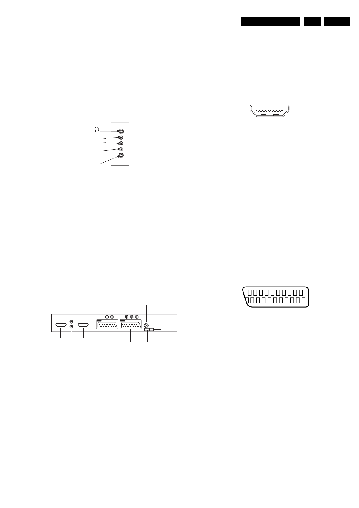
1.2.1 Side I/O connections
R
Audio
L
Video
S-Video
G_16210_070.eps
190106
Figure 1-1 Side I/O connections
S-Video (Hosiden): Video Y/C - In
1 - Ground Y Gnd H
2 - Ground C Gnd H
3 - Video Y 1 V
4 - Video C 0.3 V
Cinch: Video CVBS - In, Audio - In
Ye -Video CVBS 1 V
Wh - Audio L 0.5 V
Rd - Audio R 0.5 V
Mini Jack: Audio Head phone - Out
Bk - Head phone 32 - 600 ohm / 10 mW ot
/ 75 ohm j
PP
/ 75 ohm j
PP
/ 75 ohm jq
PP
/ 10 kohm jq
RMS
/ 10 kohm jq
RMS
Service connector (ComPair)
1 - SDA-S I
2 - SCL-S I
2
C Data (0 - 5 V) jk
2
C Clock (0 - 5 V) j
3 - Ground Gnd H
Service connector (UART)
1 - UART_TX Transmit k
2 - Ground Gnd H
3 - UART_RX Receive j
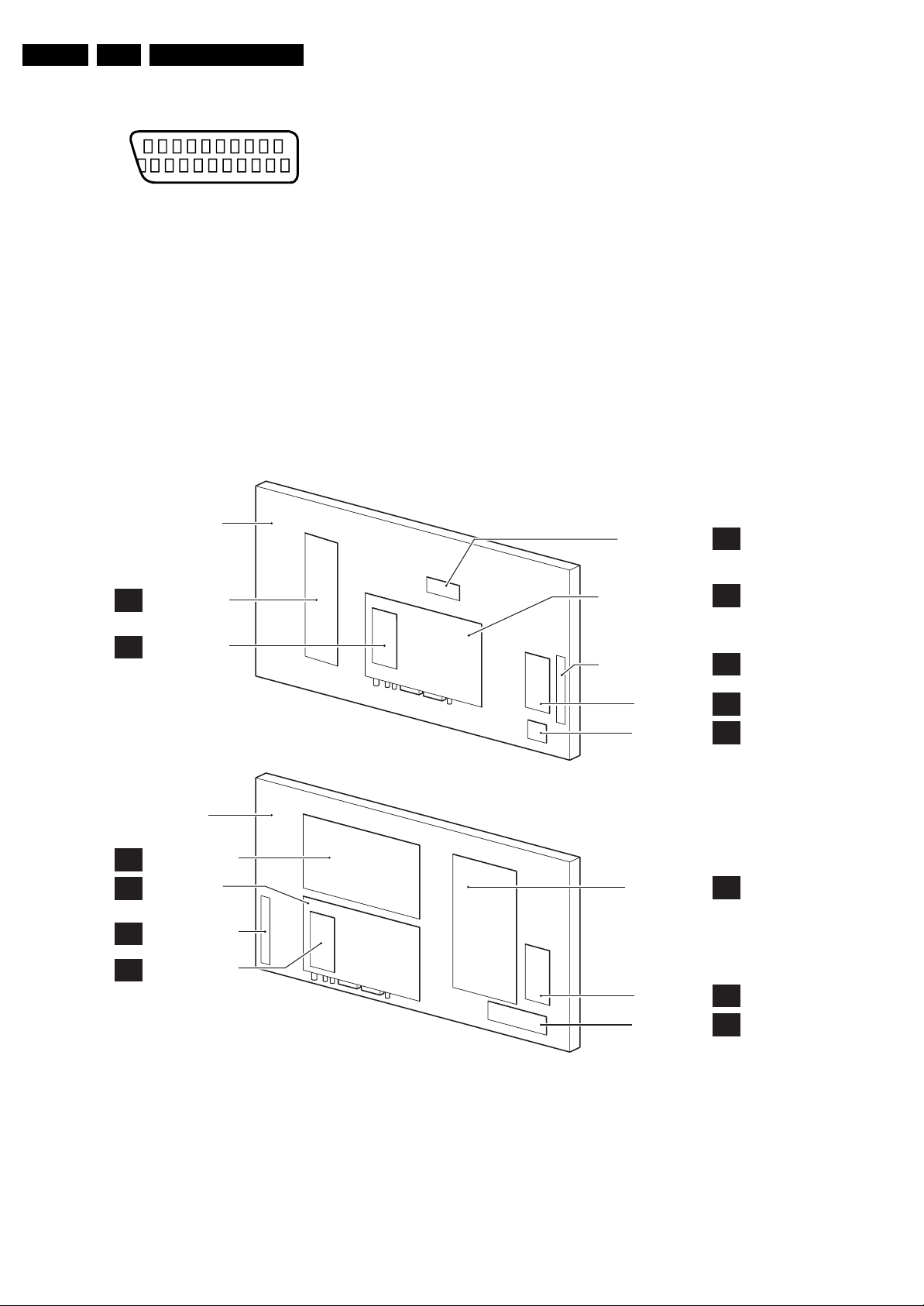
HDMI: Digital Video/Digital Audio - In
19
18 2
1
E_06532_017.eps
250505
Figure 1-3 HDMI (type A) connector
1 - D2+ Data channel j
2 - Shield Gnd H
3 - D2- Data channel j
4 - D1+ Data channel j
5 - Shield Gnd H
6 - D1- Data channel j
7 - D0+ Data channel j
8 - Shield Gnd H
9 - D0- Data channel j
10 - CLK+ Data channel j
11 - Shield Gnd H
12 - CLK- Data channel j
13 - n.c.
14 - n.c.
15 - DDC_SCL DDC clock j
16 - DDC_SDA DDC data jk
17 - Ground Gnd H
18 - +5V j
19 - HPD Hot Plug Detect j
20 - Ground Gnd H
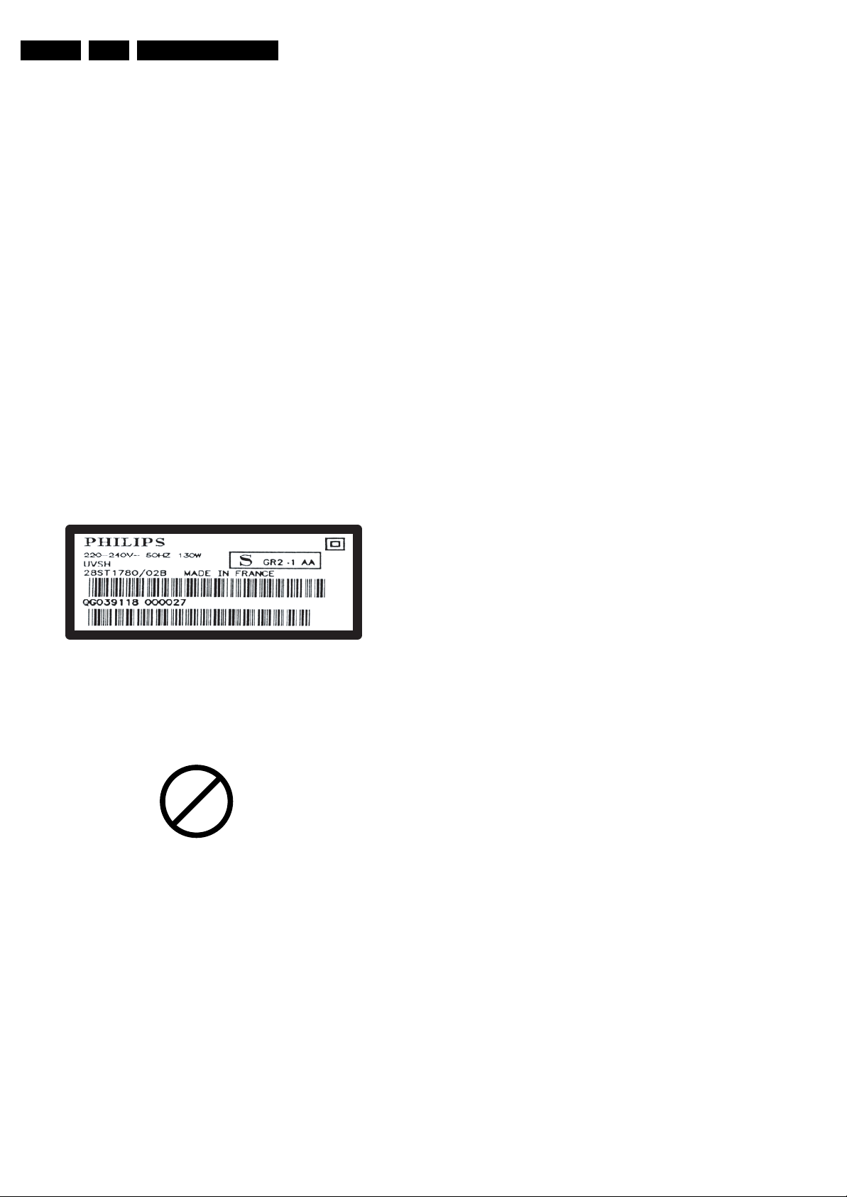
EXT1: Video RGB - In, CVBS - In/Out, Audio - In/Out
1.2.2 Rear Connections
VIDEO IN
Pr Pb Y
EXT 1
AERIAL IN
HDMI
L
DVI HDMI
AUDIO IN
AUDIO IN
RRL
EXT 2 EXT 1
EXT 2 UART I2C
Figure 1-2 Rear I/O
Aerial - In
- - IEC-type (EU) Coax, 75 ohm D
Cinch: Audio - In
Wh - Audio L 0.5 V
Rd - Audio R 0.5 V
/ 10 kohm jq
RMS
/ 10 kohm jq
RMS
Cinch: Video YPbPr - In
Gn - Video Y 1 V
Bu -Video Pb 0.7 V
Rd - Video Pr 0.7 V
/ 75 ohm jq
PP
/ 75 ohm jq
PP
/ 75 ohm jq
PP
Cinch: DVI Audio - In
Rd - Audio - R 0.5 V
Wh - Audio - L 0.5 V
/ 10 kohm jq
RMS
/ 10 kohm jq
RMS
ComPair
G_16210_071.eps
190106
21
20
E_06532_001.eps
2
1
050404
Figure 1-4 SCART connector
1 - Audio R 0.5 V
2 - Audio R 0.5 V
3 - Audio L 0.5 V
4 - Ground Audio Gnd H
/ 1 kohm k
RMS
/ 10 kohm j
RMS
/ 1 kohm k
RMS
5 - Ground Blue Gnd H
6 - Audio L 0.5 V
7 - Video Blue 0.7 V
/ 10 kohm j
RMS
/ 75 ohm j
PP
8 - Function Select 0 - 2 V: INT
4.5 - 7 V: EXT 16:9
9.5 - 12 V: EXT 4:3 j
9 - Ground Green Gnd H
10 - n.c.
11 - Video Green 0.7 V
/ 75 ohm j
PP
12 - n.c.
13 - Ground Red Gnd H
14 - Ground Gnd H
15 - Video Red 0.7 V
16 - Status/FBL 0 - 0.4 V: INT
/ 75 ohm j
PP
1 - 3 V: EXT / 75 ohm j
17 - Ground Video Gnd H
18 - Ground FBL Gnd H
19 - Video Terr. CVBS 1 V
20 - Video CVBS/Y 1 V
/ 75 ohm k
PP
/ 75 ohm j
PP
21 - Shield Gnd H
Page 4
EN 4 LC4.31E AA1.
Technical Specifications, Connections, and Chassis Overview
EXT2: Video Y/C - in, CVBS - In/Out, Audio - In/Out
21
20
E_06532_001.eps
2
1
050404
Figure 1-5 SCART connector
1 - Audio R 0.5 V
2 - Audio R 0.5 V
3 - Audio L 0.5 V
/ 1 kohm k
RMS
/ 10 kohm j
RMS
/ 1 kohm k
RMS
4 - Ground Audio Gnd H
5 - Ground Blue Gnd H
6 - Audio L 0.5 V
/ 10 kohm j
RMS
1.3 Chassis Overview
Chassis Overview 26” & 32” Models
LCD PANEL
7-n.c.
8 - Function Select 0 - 2 V: INT
4.5 - 7 V: EXT 16:9
9.5 - 12 V: EXT 4:3 j
9 - Ground Green Gnd H
10 - n.c.
11 - n.c.
12 - n.c.
13 - Ground Red Gnd H
14 - Ground Gnd H
15 - YC/C - in 0.7 V
/ 75 ohm j
PP
16 - n.c.
17 - Ground Video Gnd H
18 - Ground Gnd H
19 - Video Mon. CVBS 1 V
20 - YC/Y - in 0.7 V
21 - Shield Gnd H
/ 75 ohm k
PP
/ 75 ohm j
PP
CLASS D AUDIO
AMPLIFIER PANEL
C
POWER SUPPLY
A
PANEL
OTC TXT PANEL
T
LCD PANEL
STANDBY & AUDIO
SA
PA NE L
SMALL SIGNAL
B
BOARD
CONTROL BOARD
E
OTC TXT PANEL
T
Chassis Overview 37” & 42” Models
SMALL SIGNAL BOARD
KEYBOARD CONTROL
POWER SUPPLY
PANEL
SIDE I/O PANEL
LED & IR PANEL
UNIT
SIDE I/O PANEL
LED & IR PANEL
G_16210_072.eps
B
E
D
J
A
D
J
190506
Figure 1-6 Chassis overview
Page 5

Safety Instructions, Warnings, and Notes
2. Safety Instructions, Warnings, and Notes
EN 5LC4.31E AA 2.
Index of this chapter:
2.1 Safety Instructions
2.2 Warnings
2.3 Notes
2.1 Safety Instructions
Safety regulations require the following during a repair:
• Connect the set to the Mains (AC Power) via an isolation
transformer (> 800 VA).
• Replace safety components, indicated by the symbol h,
only by components identical to the original ones. Any
other component substitution (other than original type) may
increase risk of fire or electrical shock hazard.
Safety regulations require that after a repair, the set must be
returned in its original condition. Pay in particular attention to
the following points:
• Route the wire trees correctly and fix them with the
mounted cable clamps.
• Check the insulation of the Mains (AC Power) lead for
external damage.
• Check the strain relief of the Mains (AC Power) cord for
proper function.
• Check the electrical DC resistance between the Mains (AC
Power) plug and the secondary side (only for sets that have
a Mains (AC Power) isolated power supply):
1. Unplug the Mains (AC Power) cord and connect a wire
between the two pins of the Mains (AC Power) plug.
2. Set the Mains (AC Power) switch to the “on” position
(keep the Mains (AC Power) cord unplugged!).
3. Measure the resistance value between the pins of the
Mains (AC Power) plug and the metal shielding of the
tuner or the aerial connection on the set. The reading
should be between 4.5 Mohm and 12 Mohm.
4. Switch “off” the set, and remove the wire between the
two pins of the Mains (AC Power) plug.
• Check the cabinet for defects, to prevent touching of any
inner parts by the customer.
2.3 Notes
2.3.1 General
• Measure the voltages and waveforms with regard to the
chassis (= tuner) ground (H), or hot ground (I), depending
on the tested area of circuitry. The voltages and waveforms
shown in the diagrams are indicative. Measure them in the
Service Default Mode (see chapter 5) with a colour bar
signal and stereo sound (L: 3 kHz, R: 1 kHz unless stated
otherwise) and picture carrier at 475.25 MHz for PAL, or
61.25 MHz for NTSC (channel 3).
• Where necessary, measure the waveforms and voltages
with (D) and without (E) aerial signal. Measure the
voltages in the power supply section both in normal
operation (G) and in stand-by (F). These values are
indicated by means of the appropriate symbols.
• The semiconductors indicated in the circuit diagram and in
the parts lists, are interchangeable per position with the
semiconductors in the unit, irrespective of the type
indication on these semiconductors.
2.3.2 Schematic Notes
• All resistor values are in ohms, and the value multiplier is
often used to indicate the decimal point location (e.g. 2K2
indicates 2.2 kohm).
• Resistor values with no multiplier may be indicated with
either an "E" or an "R" (e.g. 220E or 220R indicates 220
ohm).
• All capacitor values are given in micro-farads (µ= x10
nano-farads (n= x10
• Capacitor values may also use the value multiplier as the
decimal point indication (e.g. 2p2 indicates 2.2 pF).
• An "asterisk" (*) indicates component usage varies. Refer
to the diversity tables for the correct values.
• The correct component values are listed in the Spare Parts
List. Therefore, always check this list when there is any
doubt.
-9
), or pico-farads (p= x10
-12
-6
),
).
2.2 Warnings
• All ICs and many other semiconductors are susceptible to
electrostatic discharges (ESD w). Careless handling
during repair can reduce life drastically. Make sure that,
during repair, you are connected with the same potential as
the mass of the set by a wristband with resistance. Keep
components and tools also at this same potential. Available
ESD protection equipment:
– Complete kit ESD3 (small tablemat, wristband,
connection box, extension cable and earth cable) 4822
310 10671.
– Wristband tester 4822 344 13999.
• Be careful during measurements in the high voltage
section.
• Never replace modules or other components while the unit
is switched “on”.
• When you align the set, use plastic rather than metal tools.
This will prevent any short circuits and the danger of a
circuit becoming unstable.
2.3.3 Rework on BGA (Ball Grid Array) ICs
General
Although (LF)BGA assembly yields are very high, there may
still be a requirement for component rework. By rework, we
mean the process of removing the component from the PWB
and replacing it with a new component. If an (LF)BGA is
removed from a PWB, the solder balls of the component are
deformed drastically so the removed (LF)BGA has to be
discarded.
Device Removal
As is the case with any component that, is being removed, it is
essential when removing an (LF)BGA, that the board, tracks,
solder lands, or surrounding components are not damaged. To
remove an (LF)BGA, the board must be uniformly heated to a
temperature close to the reflow soldering temperature.
A uniform temperature reduces the risk of warping the PWB. To
do this, we recommend that the board is heated until it is certain
that all the joints are molten. Then carefully pull the component
off the board with a vacuum nozzle. For the appropriate
temperature profiles, see the IC data sheet.
Area Preparation
When the component has been removed, the vacant IC area
must be cleaned before replacing the (LF)BGA.
Removing an IC often leaves varying amounts of solder on the
mounting lands. This excessive solder can be removed with
either a solder sucker or solder wick. The remaining flux can be
removed with a brush and cleaning agent.
Page 6
EN 6 LC4.31E AA2.
Safety Instructions, Warnings, and Notes
After the board is properly cleaned and inspected, apply flux on
the solder lands and on the connection balls of the (LF)BGA.
Note: Do not apply solder paste, as this has been shown to
result in problems during re-soldering.
Device Replacement
The last step in the repair process is to solder the new
component on the board. Ideally, the (LF)BGA should be
aligned under a microscope or magnifying glass. If this is not
possible, try to align the (LF)BGA with any board markers.
So as not to damage neighbouring components, it may be
necessary to reduce some temperatures and times.
More Information
For more information on how to handle BGA devices, visit this
URL: www.atyourservice.ce.philips.com (needs subscription,
not available for all regions). After login, select “Magazine”,
then go to “Repair downloads”. Here you will find Information
on how to deal with BGA-ICs.
2.3.4 Lead-free Solder
Philips CE is producing lead-free sets (PBF) from 1.1.2005
onwards.
Identification: The bottom line of a type plate gives a 14-digit
serial number. Digits 5 and 6 refer to the production year, digits
7 and 8 refer to production week (in example below it is 1991
week 18).
To avoid wear-out of tips, switch “off” unused equipment or
reduce heat.
• Mix of lead-free soldering tin/parts with leaded soldering
tin/parts is possible but PHILIPS recommends strongly to
avoid mixed regimes. If this cannot be avoided, carefully
clear the solder-joint from old tin and re-solder with new tin.
• Use only original spare-parts listed in the Service-Manuals.
Not listed standard material (commodities) has to be
purchased at external companies.
• Special information for lead-free BGA ICs: these ICs will be
delivered in so-called "dry-packaging" to protect the IC
against moisture. This packaging may only be opened
shortly before it is used (soldered). Otherwise the body of
the IC gets "wet" inside and during the heating time the
structure of the IC will be destroyed due to high (steam-)
pressure inside the body. If the packaging was opened
before usage, the IC has to be heated up for some hours
(around 90°C) for drying (think of ESD-protection!).
Do not re-use BGAs at all!
• For sets produced before 1.1.2005, containing leaded
soldering tin and components, all needed spare parts will
be available till the end of the service period. For the repair
of such sets nothing changes.
In case of doubt whether the board is lead-free or not (or with
mixed technologies), you can use the following method:
• Always use the highest temperature to solder, when using
SAC305 (see also instructions below).
• De-solder thoroughly (clean solder joints to avoid the
mixing of two alloys).
E_06532_024.eps
230205
Figure 2-1 Serial number example
Regardless of the special lead-free logo (which is not always
indicated), one must treat all sets from this date onwards
according to the rules as described below.
P
b
Figure 2-2 Lead-free logo
Due to lead-free technology some rules have to be respected
by the workshop during a repair:
• Use only lead-free soldering tin Philips SAC305 with order
code 0622 149 00106. If lead-free solder paste is required,
please contact the manufacturer of your soldering
equipment. In general, use of solder paste within
workshops should be avoided because paste is not easy to
store and to handle.
• Use only adequate solder tools applicable for lead-free
soldering tin. The solder tool must be able:
– To reach a solder-tip temperature of at least 400°C.
– To stabilise the adjusted temperature at the solder-tip.
– To exchange solder-tips for different applications.
• Adjust your solder tool so that a temperature of around
360°C - 380°C is reached and stabilised at the solder joint.
Heating time of the solder-joint should not exceed ~ 4 sec.
Avoid temperatures above 400°C, otherwise wear-out of
tips will increase drastically and flux-fluid will be destroyed.
Caution: For BGA-ICs, you must use the correct temperature
profile, which is coupled to the 12NC. For an overview of these
profiles, visit the website www.atyourservice.ce.philips.com
(needs subscription, but is not available for all regions).
You will find this and more technical information within the
“Magazine”, chapter “Repair downloads”.
For additional questions please contact your local repair help
desk.
2.3.5 Alternative BOM identification
In September 2003, Philips CE introduced a change in the way
the serial number (or production number, see Figure 2-1) is
composed. From this date on, the third digit in the serial
number (example: AG2B0335000001) indicates the number of
the alternative BOM (Bill of Materials used for producing the
specific model of TV set). It is possible that the same TV model
on the market is produced with e.g. two different types of
displays, coming from two different O.E.M.s.
By looking at the third digit of the serial number, the service
technician can see if there is more than one type of B.O.M.
used in the production of the TV set he is working with. He can
then consult the At Your Service Web site, where he can type
in the Commercial Type Version Number of the TV set (e.g.
28PW9515/12), after which a screen will appear that gives
information about the number of alternative B.O.M.s used.
If the third digit of the serial number contains the number 1
(example: AG1B033500001), then there is only one B.O.M.
version of the TV set on the market. If the third digit is a 2
(example: AG2B0335000001), then there are two different
B.O.M.s. Information about this is important for ordering
the correct spare parts!
For the third digit, the numbers 1...9 and the characters A...Z
can be used, so in total: 9 plus 26 = 35 different B.O.M.s can
be indicated by the third digit of the serial number.
2.3.6 Practical Service Precautions
• It makes sense to avoid exposure to electrical shock.
While some sources are expected to have a possible
dangerous impact, others of quite high potential are of
limited current and are sometimes held in less regard.
Page 7

Directions for Use
EN 7LC4.31E AA 3.
• Always respect voltages. While some may not be
dangerous in themselves, they can cause unexpected
reactions that are best avoided. Before reaching into a
3. Directions for Use
You can download this information from the following websites:
http://www.philips.com/support
http://www.p4c.philips.com
powered TV set, it is best to test the high voltage insulation.
It is easy to do, and is a good service precaution.
Page 8
EN 8 LC4.31E AA4.
Mechanical Instructions
4. Mechanical Instructions
Index of this chapter:
4.1 Cable Dressing
4.2 Service Position
4.3 Assy/Panel Removal
4.4 Set Re-assembly
4.1 Cable Dressing
Notes:
• Figures below can deviate slightly from the actual situation,
due to the different set executions.
• Follow the disassembling instructions in described order.
4.2 Service Position
First, put the TV set in its service position. Therefore, place it
upside down on a table top (use a protection sheet or foam
bars).
4.2.1 The Foam Bars
E_06532_018.eps
Figure 4-2 Foam bars
Figure 4-1 Cable dressing (26PF5321/10)
placing a mirror flat on the table under the TV you can easily
see if something is happening on the screen.
4.3 Assy/Panel Removal
4.3.1 Rear Cover
Warning: Disconnect the mains power cord before you remove
the rear cover.
1. Remove the screws that secure the rear cover.
2. Lift the rear cover from the cabinet cautiously. Make sure
that wires and other internal components are not damaged
during cover removal.
170504
G_16210_073.eps
190106
The foam bars (order code 3122 785 90580) can be used for
all types and sizes of Flat TVs. By laying the plasma or LCD TV
flat on the (ESD protective) foam bars, a stable situation is
created to perform measurements and alignments. By first
Page 9
Mechanical Instructions
EN 9LC4.31E AA 4.
4.3.2 Side I/O Panel
1
Figure 4-3 Side I/O panel
1. Disconnect the cable [1] from the panel.
2. Release the two fixation clamps [2] and lift the panel out of
the bracket.
2
2
G_16210_074.eps
190106
4.3.4 Keyboard Control Panel
1
4
3
2
3
2
3
4.3.3 LED Panel
Figure 4-4 LED panel
1. Release the fixation clamp [1] and take the panel out of the
bracket.
2. Disconnect the cable [2] from the panel.
2
1
G_16210_075.eps
190106
Figure 4-5 Keyboard control panel
1. Remove the two fixation screws [1] from the bracket and
take out the panel/bracket combination.
2. Remove the fixation tape [2] from the panel/bracket
combination.
3. Release the three fixation clamps [3] and lift the panel out
of the bracket.
4. Disconnect the cable [4] from the panel.
4.3.5 SSB Cover Shield (depending on model)
1
G_16210_076.eps
190106
1
Figure 4-6 Cable clip on cover shield
F_15270_044.eps
180505
Page 10
EN 10 LC4.31E AA4.
2
2
Figure 4-7 SSB cover shield
1. Release the cable from the plastic cable clip [1] on the
shield (see Figure “Cable clip on cover shield” above).
2. Remove the four fixation screws (2, see Figure “SSB cover
shield”; the screws are also indicated by arrows on the
shield) and remove the shield.
Notice that on one side, the shield is not only held by two
screws, but also by two brackets (see Figure “Cable clip on
cover shield” above).
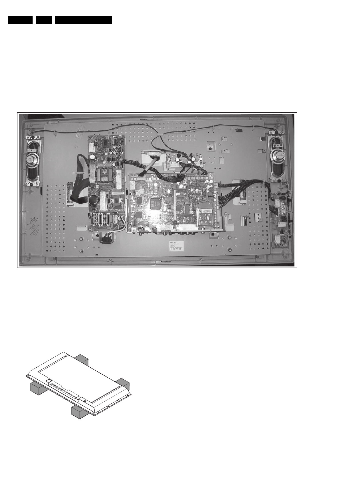
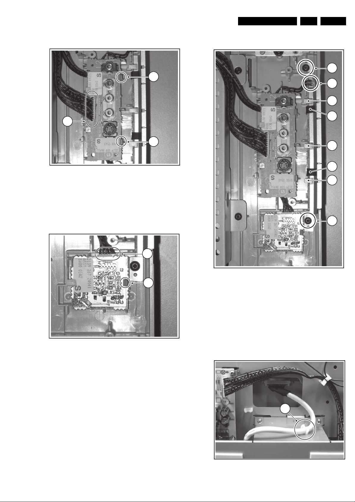
4.3.6 Small Signal Board
Mechanical Instructions
4.3.7 Power Supply Panel (various models used)
F_15270_045.eps
190505
1. Very cautiously disconnect the LVDS cable [1] from the
panel (see Figure “SSB connectors”). Notice that this cable
is very fragile.
2. Disconnect the other cables [2] from the panel.
3. Remove the fixation screws [3] that secure the SSB
(depending on model) and also the fixation screws [4] from
the connector plate (see Figure “Connector screws”).
4. Take the panel out of its brackets.
1
1
2
3
1
3
Figure 4-8 SSB connectors
4
4 4
4
4 4
2
4
3
3
G_16210_077.eps
190106
1
2
G_16210_079.eps
Figure 4-10 Power supply panel
1. Disconnect all cables [1] from the panel.
Notice that the two connectors for X520 and X530 on
this panel are similar, and should not be mixed up later
when they are reconnected (X520 is connected via its
flatcable to connector CN01 on the LCD panel, near the Rspeaker; X530 is connected via its flatcable to connector
CN04 on the LCD panel, near the L-speaker).
2. Remove the fixation screws [2] from the panel.
3. Take the panel out of its brackets.
200106
Figure 4-9 Connector screws
G_16210_078.eps
200106
Page 11
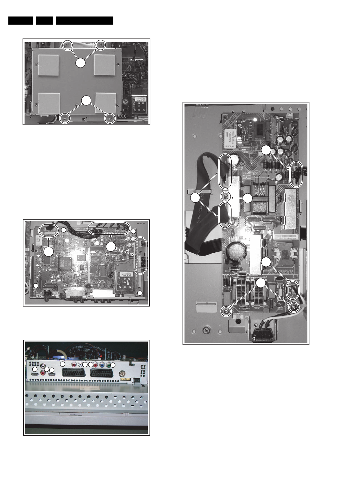
4.3.8 Audio Amplifier Panel
00106
Mechanical Instructions
2
EN 11LC4.31E AA 4.
2
1
Figure 4-11 Audio amplifier panel
1. Disconnect all cables [1] from the panel.
2. Remove the fixation screws [2] from the panel.
3. Remove the panel.
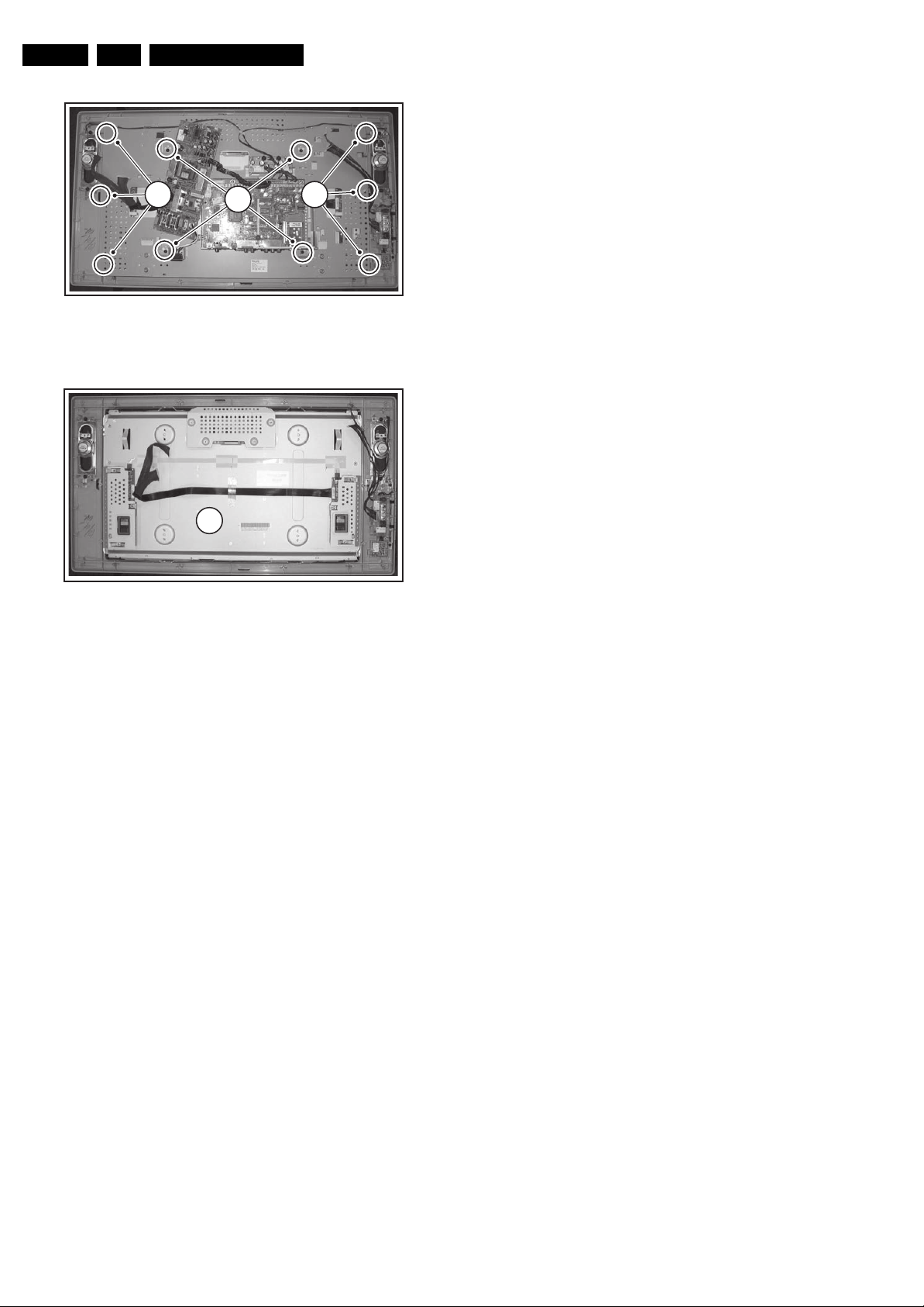
4.3.9 LCD Panel
G_16210_080.eps
200106
1
3
G_16210_083.eps
200106
Figure 4-14 SSB connectors for side I/O, side control panel, and
LED
Figure 4-12 Loudspeaker cables
Figure 4-13 LVDS connector
G_16210_081.eps
2
G_16210_082.eps
200106
2
4
5
G_16210_084.eps
200106
Figure 4-15 Connectors X520 and X530 and fixation screws on
power supply panel
Page 12
EN 12 LC4.31E AA4.
Mechanical Instructions
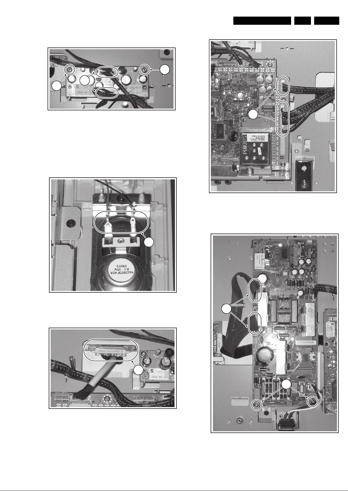
4.4 Set Re-assembly
To re-assemble the whole set, execute all processes in reverse
order.
6
7
6
G_16210_085.eps
Figure 4-16 Shield screws of the LCD panel
8
G_16210_086.eps
Notes:
• While re-assembling, make sure that all cables are placed
and connected in their original positions. See Figure “Cable
dressing”.
Be careful with the fragile LVDS cable.
200106
200106
Figure 4-17 LCD panel
To remove the LCD-panel, carry out the following steps:
1. Disconnect the cables [1] from the “L” and the “R”
loudspeakers (see Figure “Loudspeaker cables”).
2. Important: Unplug the LVDS connector [2] on the LCD
panel (see Figure “LVDS connector”), or better: remove the
cable completely.
Be careful, as this is a very fragile connector/cable!
3. Unplug the connectors [3] of the Side I/O panel, the Top
Control panel, and the LED panel on the SSB (see Figure
“SSB connectors for side I/O, side control panel, and
LED”).
4. Unplug the connectors X520 and X530 [4] on the Power
Supply board (see Figure “Connectors X520 and X530 and
fixation screws on power supply panel”).
5. Loosen the fixation screws [5] from the power supply
board, and put the power supply board a bit aside.
6. Loosen screws [6] and [7] (see Figure “Shield screws of the
LCD panel”).
7. Lift the metal frame (together with all PWBs) from the LCD
panel.
Take care not to damage the fragile LVDS cable.
8. After removal of the metal frame, you can lift the LCD
display [8] from its plastic frame (see Figure “LCD panel”).
9. If the plastic frame is damaged, replace it by a new frame,
after removing the loudspeakers, the Side I/O panel, the
Side Control panel, and the LED panel.
Page 13
Service Modes, Error Codes, and Fault Finding
5. Service Modes, Error Codes, and Fault Finding
EN 13LC4.31E AA 5.
Index of this chapter:
5.1 Test Points
5.2 Service Modes
5.3 Problems and Solving Tips Related to CSM
5.4 Service Tools
5.5 Error Codes
5.6 The Blinking LED Procedure
5.7 Fault Finding and Repair Tips
5.1 Test Points
This chassis is equipped with test points. In the schematics,
test points are indicated with a rectangle box around Fxxx or
Ixxx, in the layouts with a half-moon.
Perform measurements under the following conditions:
• Television set in Service Default Mode.
• Video input: Colour bar signal.
• Audio input: 3 kHz left channel, 1 kHz right channel.
5.2 Service Modes
Service Default mode (SDM) and Service Alignment Mode
(SAM) offer several features for the service technician, while
the Customer Service Mode (CSM) is used for communication
between the call centre and the customer.
This chassis also offers the option of using ComPair, a
hardware interface between a computer and the TV chassis. It
offers the possibilities of structured troubleshooting, error code
reading, and software version read-out for all chassis.
Minimum requirements for ComPair: a Pentium processor, a
Windows OS, and a CD-ROM drive (see also paragraph
"ComPair").
How to Enter
To enter SDM, use one of the following methods:
• Press the following key sequence on the remote control
transmitter: “062596” directly followed by the MENU button
(do not allow the display to time out between entries while
keying the sequence).
• Short one of the "Service" jumpers on the TV board during
cold start and apply mains (see Figures "Service jumper").
Then press the mains button (remove the short after startup).
Caution: Entering SDM by shorting "Service" jumpers will
override the +8V-protection. Do this only for a short period.
When doing this, the service-technician must know exactly
what he is doing, as it could damage the television set.
• Or via ComPair.
SDM
G_16210_087.eps
200106
Figure 5-1 Service jumper (component side)
5.2.1 Service Default Mode (SDM)
Purpose
• To create a predefined setting for measurements to be
made.
• To override software protections.
• To start the blinking LED procedure.
• To inspect the error buffer.
• To check the life timer.
Specifications
• Tuning frequency: 475.25 MHz.
• Colour system: PAL-BG.
• All picture settings at 50% (brightness, colour contrast,
hue).
• Bass, treble, and balance at 50 %; volume at 25 %.
• All service-unfriendly modes (if present) are disabled. The
service unfriendly modes are:
– Timer / Sleep timer.
– Child / parental lock.
– Blue mute.
– Hotel / hospital mode.
– Auto shut off (when no “IDENT” video signal is
received for 15 minutes).
– Skipping of non-favourite presets / channels.
– Auto-storage of personal presets.
– Auto user menu time-out.
– Auto Volume Levelling (AVL).
SDM
G_16210_088.eps
200106
Figure 5-2 Service jumper (solder side)
After entering SDM, the following screen is visible, with SDM in
the upper right corner of the screen to indicate that the
television is in Service Default Mode.
Page 14
EN 14 LC4.31E AA5.
00035 HSD21E1 1.00/S21LXN 1.00 SDM
ERR 0 0 0 0 0
OP 152 167 015 081 252 127 019
Figure 5-3 SDM menu
Service Modes, Error Codes, and Fault Finding
After entering SAM, the following screen is visible, with SAM in
the upper right corner of the screen to indicate that the
television is in Service Alignment Mode.
00035 HSD21E1 1.00/S21LXN 1.00 SAM
ERR 0 0 0 0 0
OP 152 167 015 081 252 127 019
. Clear Clear ?
. Options
. Tuner
. White Tone
. Audio
. NVM Editor
G_16210_089.eps
200106
. SC NVM Editor
. ComPair Mode On
G_16210_090.eps
200106
How to Navigate
Use one of the following methods:
• When you press the MENU button on the remote control,
the set will switch on the normal user menu in the SDM
mode.
• On the TV, press and hold the VOLUME DOWN and press
the CHANNEL DOWN for a few seconds, to switch from
SDM to SAM and reverse; or press the following key
sequence on the remote control transmitter: “062596”
directly followed by the OSD button to switch to SAM (do
not allow the display to time out between entries while
keying the sequence).
How to Exit
Switch the set to STANDBY by pressing the mains button on
the remote control transmitter or the television set.
If you turn the television set off by removing the mains (i.e.,
unplugging the television) without using the mains button, the
television set will remain in SDM when mains is re-applied, and
the error buffer is not cleared.
5.2.2 Service Alignment Mode (SAM)
Purpose
• To change option settings.
• To display / clear the error code buffer.
• To perform alignments.
Specifications
• Operation hours counter (maximum five digits displayed).
• Software version, Error codes, and Option settings display.
• Error buffer clearing.
• Option settings.
• Software alignments (Tuner, White Tone, Geometry &
Audio).
• NVM Editor.
• ComPair Mode switching.
How to Enter
To enter SAM, use one of the following methods:
• Press the following key sequence on the remote control
transmitter: “062596" directly followed by the OSD/
STATUS/INFO(I+) button (do not allow the display to time
out between entries while keying the sequence).
• Or via ComPair.
Figure 5-4 SAM menu
Menu Explanation
1. LLLLL. This represents the run timer. The run timer counts
normal operation hours, but does not count standby hours.
2. AAABCD X.YY. This is the software identification of the
main microprocessor:
– A= the project name (LC04.x).
– B= the region: E= Europe, A= Asia Pacific, U= NAFTA,
L= LATAM.
– C= the software diversity:
• Europe: T= 1 page TXT, F= Full TXT, V= Voice
control.
• LATAM and NAFTA: N= Stereo non-dBx, S=
Stereo dBx.
• Asian Pacific: T= TXT, N= non-TXT, C= NTSC.
• ALL regions: M= mono, D= DVD, Q= Mk2.
– D= the language cluster number.
– X= the main software version number (updated with a
major change that is incompatible with previous
versions).
– Y= the sub software version number (updated with a
minor change that is compatible with previous
versions).
3. EEEEE F.GG. This is the software identification of the
Scaler:
– EEEEEE= the scaler sw cluster
– F= the main sw version no.
– GG= the sub-version no.
4. SAM. Indication of the Service Alignment Mode.
5. Error Buffer. Shows all errors detected since the last time
the buffer was erased. Five errors possible.
6. Option Bytes. Used to read-out the option bytes. See
“Options” in the Alignments section for a detailed
description. Seven codes are possible.
7. Clear. Erases the contents of the error buffer. Select the
CLEAR menu item and press the MENU RIGHT key. The
content of the error buffer is cleared.
8. Options. Used to set the option bits. See “Options” in the
Alignments section for a detailed description.
9. Tuner. Used to align the tuner. See “Tuner” in the
Alignments section for a detailed description.
10. White Tone. Used to align the white tone. See “White
Tone” in the Alignments section for a detailed description.
11. Audio. No audio alignment is necessary for this television
set.
12. NVM Editor. Can be used to change the NVM data in the
television set. See table “NVM data” further on.
Page 15

Service Modes, Error Codes, and Fault Finding
13. SC NVM Editor. Can be used to edit Scaler NVM.
14. ComPaIr. Can be used to switch on the television to In
System Programming (ISP) mode, for software uploading
via ComPair.
Caution: When this mode is selected without ComPair
connected, the TV will be blocked. Remove the AC power
to reset the TV.
How to Navigate
• In SAM, select menu items with the MENU UP/DOWN keys
on the remote control transmitter. The selected item will be
indicated. When not all menu items fit on the screen, use
the MENU UP/DOWN keys to display the next / previous
menu items.
• With the MENU LEFT/RIGHT keys, it is possible to:
– Activate the selected menu item.
– Change the value of the selected menu item.
– Activate the selected submenu.
• In SAM, when you press the MENU button twice, the set
will switch to the normal user menus (with the SAM mode
still active in the background). To return to the SAM menu
press the MENU button.
• When you press the MENU key in while in a submenu, you
will return to the previous menu.
• On the TV, press and hold the VOLUME DOWN and press
the CHANNEL DOWN for a few seconds, to switch from
SAM to SDM and reverse; or press the following key
sequence on the remote control transmitter: “062596”
directly followed by the MENU button to switch to SDM (do
not allow the display to time out between entries while
keying the sequence).
How to Store SAM Settings
To store the settings changed in SAM mode, leave the top level
SAM menu by using the POWER button on the remote control
transmitter or the television set.
How to Exit
Switch the set to STANDBY by pressing the mains button on
the remote control transmitter or the television set.
If you turn the television set “off” by removing the mains (i.e.,
unplugging the television) without using the mains button, the
television set will remain in SAM when mains is re-applied, and
the error buffer is not cleared.
5.2.3 Customer Service Mode (CSM)
EN 15LC4.31E AA 5.
1 00035 HSD21E1 1.00/S21LXN 1.00 CSM
2 CODES 0 0 0 0 0
3 OP 152 167 015 081 252 127 019
4 26PF5321/10
5 AAAAAA/B.CC
6 NOT TUNED
7 PAL
8 STEREO
9 CO 50 CL 50 BR 50
0 AVL Off
G_16210_091.eps
200106
Figure 5-5 CSM menu
Menu Explanation
1. Indication of the decimal value of the operation hours
counter, Main/Scaler software version (see “Service
Alignment Mode" for an explanation), and the service mode
(CSM = Customer Service Mode).
2. Displays the last five errors detected in the error code
buffer.
3. Displays the option bytes.
4. Displays the type number version of the set.
5. aaaaaa / b.ccc Firmware identification of the Pacific 3 and
the OTC:
– aaaaaa = the firmware version of the Pacific 3 (Pixel+)
– b.ccc = the firmware version of the OTC (for the 1000
page TXT decoder).
6. Indicates the television is receiving an "IDENT" signal on
the selected source. If no "IDENT" signal is detected, the
display will read "NOT TUNED".
7. Displays the detected Colour system (e.g. PAL/NTSC).
8. Displays the detected Audio (e.g. stereo/mono).
9. Displays the picture setting information.
10. Displays the sound setting information.
Purpose
The Customer Service Mode shows error codes and
information on the TV’s operation settings. The call centre can
instruct the customer (by telephone) to enter CSM in order to
identify the status of the set. This helps the call centre to
diagnose problems and failures in the TV set before making a
service call.
The CSM is a read-only mode; therefore, modifications are not
possible in this mode.
How to Enter
To enter CSM, press the following key sequence on the remote
control transmitter: “123654” (do not allow the display to time
out between entries while keying the sequence).
Upon entering the Customer Service Mode, the following
screen will appear:
How to Exit
To exit CSM, use one of the following methods:
• Press the MENU button twice, or POWER button on the
remote control transmitter.
• Press the POWER button on the television set.
5.3 Problems and Solving Tips Related to CSM
5.3.1 Picture Problems
Note: The problems described below are all related to the TV
settings. The procedures used to change the value (or status)
of the different settings are described.
Picture too Dark or too Bright
If:
• The picture improves when you press the SMART
PICTURE button on the remote control transmitter, or
• The picture improves when you enter the Customer
Service Mode,
Page 16

EN 16 LC4.31E AA5.
Service Modes, Error Codes, and Fault Finding
Then:
1. Press the SMART PICTURE button on the remote control
transmitter repeatedly (if necessary) to choose
PERSONAL picture mode.
2. Press the MENU button on the remote control transmitter.
This brings up the normal user menu.
3. In the normal user menu, use the MENU UP/DOWN keys
to select the PICTURE sub menu.
4. Press the MENU LEFT/RIGHT keys to enter the PICTURE
sub menu.
5. Use the MENU UP/DOWN keys (if necessary) to select
BRIGHTNESS.
6. Press the MENU LEFT/RIGHT keys to increase or
decrease the value of the selected parameter.
7. Use the MENU UP/DOWN keys to select STORE.
8. Press the MENU RIGHT key to store the new value.
9. Press the MENU key to exit the PERSONAL picture mode.
White Line around Picture Elements and Text
If:
The picture improves after you have pressed the SMART
PICTURE button on the remote control transmitter,
Then:
1. Press the SMART PICTURE button on the remote control
transmitter repeatedly (if necessary) to choose
PERSONAL picture mode.
2. Press the MENU button on the remote control transmitter.
This brings up the normal user menu.
3. In the normal user menu, use the MENU UP/DOWN keys
to select the PICTURE sub menu.
4. Press the MENU LEFT/RIGHT keys to enter the PICTURE
sub menu.
5. Use the MENU UP/DOWN keys (if necessary) to select
SHARPNESS.
6. Press the MENU LEFT/RIGHT keys to increase or
decrease the value of the selected parameter.
7. Use the MENU UP/DOWN keys to select STORE.
8. Press the MENU RIGHT key to store the new value.
9. Press the MENU key to exit the PERSONAL picture mode.
Snowy Picture
Check CSM line 6. If this line reads “Not Tuned”, check the
following:
• Antenna not connected. Connect the antenna.
• No antenna signal or bad antenna signal. Connect a proper
antenna signal.
• The tuner is faulty (in this case line 2, the Error Buffer line,
will contain error number 10). Check the tuner and replace/
repair the tuner if necessary.
Black and White Picture
If:
• The picture improves after you have pressed the SMART
PICTURE button on the remote control transmitter,
Then:
1. Press the SMART PICTURE button on the remote control
transmitter repeatedly (if necessary) to choose
PERSONAL picture mode.
2. Press the MENU button on the remote control transmitter.
This brings up the normal user menu.
3. In the normal user menu, use the MENU UP/DOWN keys
to select the PICTURE sub menu.
4. Press the MENU LEFT/RIGHT keys to enter the PICTURE
sub menu.
5. Use the MENU UP/DOWN keys (if necessary) to select
COLOUR.
6. Press the MENU LEFT/RIGHT keys to increase or
decrease the value of the selected parameter.
7. Use the MENU UP/DOWN keys to select STORE.
8. Press the MENU RIGHT key to store the new value.
9. Press the MENU key to exit the PERSONAL picture mode.
5.4 Service Tools
5.4.1 ComPair
Introduction
ComPair (Computer Aided Repair) is a service tool for Philips
Consumer Electronics products. ComPair is a further
development on the European DST (service remote control),
which allows faster and more accurate diagnostics. ComPair
has three big advantages:
1. ComPair helps you to quickly get an understanding on how
to repair the chassis in a short time by guiding you
systematically through the repair procedures.
2. ComPair allows very detailed diagnostics (on I
is therefore capable of accurately indicating problem areas.
You do not have to know anything about I
yourself because ComPair takes care of this.
3. ComPair speeds up the repair time since it can
automatically communicate with the chassis (when the
microprocessor is working) and all repair information is
directly available. When ComPair is installed together with
the Force/SearchMan electronic manual of the defective
chassis, schematics and PWBs are only a mouse click
away.
Specifications
ComPair consists of a Windows based fault finding program
and an interface box between PC and the (defective) product.
The ComPair interface box is connected to the PC via a serial
(or RS-232) cable.
For this chassis, the ComPair interface box and the TV
communicate via a bi-directional service cable via the service
connector(s).
The ComPair fault finding program is able to determine the
problem of the defective television. ComPair can gather
diagnostic information in two ways:
• Automatically (by communicating with the television):
ComPair can automatically read out the contents of the
entire error buffer. Diagnosis is done on I
ComPair can access the I
ComPair can send and receive I
the micro controller of the television. In this way, it is
possible for ComPair to communicate (read and write) to
devices on the I
2
C/UART buses of the TV-set.
• Manually (by asking questions to you): Automatic
diagnosis is only possible if the micro controller of the
television is working correctly and only to a certain extent.
When this is not the case, ComPair will guide you through
the fault finding tree by asking you questions (e.g. Does the
screen give a picture? Click on the correct answer: YES /
NO) and showing you examples (e.g. Measure test-point I7
and click on the correct oscillogram you see on the
oscilloscope). You can answer by clicking on a link (e.g.
text or a waveform picture) that will bring you to the next
step in the fault finding process.
By a combination of automatic diagnostics and an interactive
question / answer procedure, ComPair will enable you to find
most problems in a fast and effective way.
2
C/UART bus of the television.
2
C/UART commands to
2
C level) and
2
C commands
2
C/UART level.
Page 17
Service Modes, Error Codes, and Fault Finding
EN 17LC4.31E AA 5.
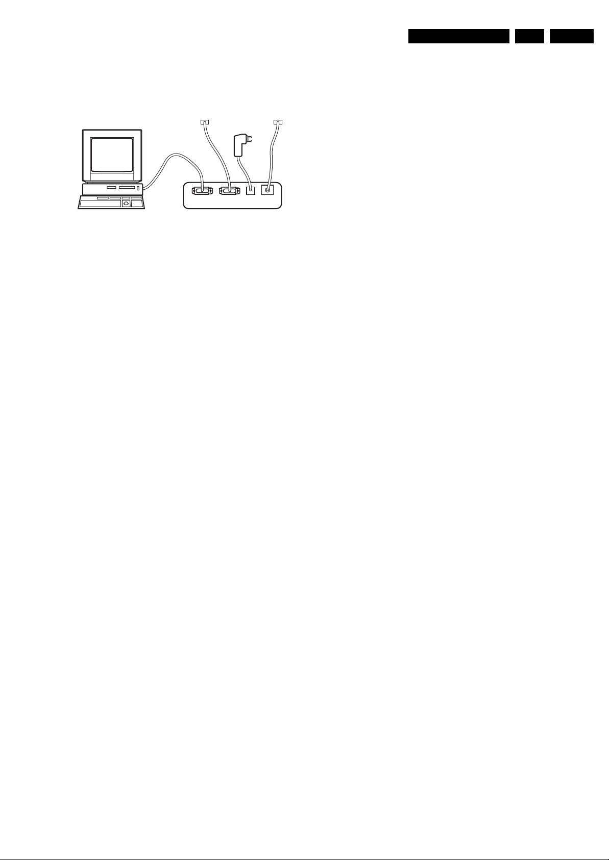
How to Connect
This is described in the chassis fault finding database in
ComPair.
TO
UART SERVICE
CONNECTOR
PC VCR I2CPo wer
9V DC
E_06532_021.eps
TO
I2C SERVICE
CONNECTOR
180804
Figure 5-6 ComPair interface connection
How to Order
• ComPair order codes (EU/AP/LATAM):
• Starter kit ComPair32/SearchMan32 software and
ComPair interface (excl. transformer): 3122 785 90450.
• ComPair interface (excl. transformer): 4822 727 21631.
• Starter kit ComPair32 software (registration version): 3122
785 60040.
• Starter kit SearchMan32 software: 3122 785 60050.
• ComPair32 CD (update): 3122 785 60070 (year 2002),
3122 785 60110 (year 2003 onwards).
• SearchMan32 CD (update): 3122 785 60080 (year 2002),
3122 785 60120 (year 2003), 3122 785 60130 (year 2004).
• ComPair firmware upgrade IC: 3122 785 90510.
• Transformer (non-UK): 4822 727 21632.
• Transformer (UK): 4822 727 21633.
• ComPair interface cable: 3122 785 90004.
• ComPair interface extension cable: 3139 131 03791.
• ComPair UART interface cable: 3122 785 90630.
Note: To use the LVDS tool, you must have ComPair release
2004-1 (or later) on your PC (engine version >= 2.2.05).
For every TV type number and screen size, one must choose
the proper settings via ComPair. The ComPair file will be
updated regularly with new introduced chassis information.
How to Order
• LVDS tool (incl. two LVDS cables: 31p and 20p):
3122 785 90671.
• LVDS tool Service Manual:
3122 785 00810.
• LVDS cable 30p (for LC4.3):
3122 785 90821 (available soon).
• LVDS cable 41p -> 31p for HD PDPs (dual -> single LVDS):
3122 785 90831 (available soon).
5.5 Error Codes
The error code buffer contains all errors detected since the last
time the buffer was erased. The buffer is written from left to
right. When an error occurs that is not yet in the error code
buffer, it is displayed at the left side and all other errors shift one
position to the right.
5.5.1 How to Read the Error Buffer
You can read the error buffer in 3 ways:
• On screen via the SAM (if you have a picture).
Examples:
– ERROR: 0 0 0 0 0 : No errors detected
– ERROR: 6 0 0 0 0 : Error code 6 is the last and only
detected error
– ERROR: 9 6 0 0 0 : Error code 6 was detected first and
error code 9 is the last detected (newest) error
• Via the blinking LED procedure (when you have no
picture). See “The Blinking LED Procedure”.
•Via ComPair.
Note: If you encounter any problems, contact your local
support desk.
5.4.2 LVDS Tool
Introduction
This service tool (also called “ComPair Assistant 1“) may help
you to identify, in case the TV does not show any picture,
whether the Small Signal Board (SSB) or the display of a Flat
TV is defective.
Furthermore it is possible to program EPLDs with this tool (Byte
blaster). Read the user manual for an explanation of this
feature.
Since 2004, the LVDS output connectors in our Flat TV models
are standardised (with some exceptions). With the two
delivered LVDS interface cables (31p and 20p) you can cover
most chassis (in special cases, an extra cable will be offered).
When operating, the tool will show a small (scaled) picture on
a VGA monitor. Due to a limited memory capacity, it is not
possible to increase the size when processing high-resolution
LVDS signals (> 1280x960). Below this resolution, or when a
DVI monitor is used, the displayed picture will be full size.
Generally this tool is intended to determine if the SSB is
working or not. Thus to determine if LVDS, RGB, and sync
signals are okay.
How to Connect
Connections are explained in the user manual, which is packed
with the tool.
5.5.2 How to Clear the Error Buffer
The error code buffer is cleared in the following cases:
• By using the CLEAR command in the SAM menu:
– To enter SAM, press the following key sequence on the
remote control transmitter: “062596” directly followed
by the OSD/i+ button (do not allow the display to time
out between entries while keying the sequence).
– Make sure the menu item CLEAR is selected. Use the
MENU UP/DOWN buttons, if necessary.
– Press the MENU RIGHT button to clear the error
buffer. The text on the right side of the “CLEAR” line will
change from “CLEAR?” to “CLEARED”
• If the contents of the error buffer have not changed for 50
hours, the error buffer resets automatically.
Note: If you exit SAM by disconnecting the mains from the
television set, the error buffer is not reset.
5.5.3 Error Codes
In case of non-intermittent faults, write down the errors present
in the error buffer and clear the error buffer before you begin
the repair. This ensures that old error codes are no longer
present.
If possible, check the entire contents of the error buffer. In
some situations, an error code is only the result of another error
and not the actual cause of the problem (for example, a fault in
the protection detection circuitry can also lead to a protection).
Page 18
EN 18 LC4.31E AA5.
Service Modes, Error Codes, and Fault Finding
Table 5-1 Error code overview
Error Error Description Check Item Diagram
0 No Error
1 Mis-match of TV (Hercules)
SW and Scaler SW
Software
versions
N.A.
2 +12V from PSU error PSU A
3Plasma I
2
C error (only for
N.A. N.A.
plasma sets)
2
C error while
4I
7801 B7 + B8
communicating with the
Genesis Scaler
5 +5V protection 7752 B6
6 General I
communication between
ADC, analogue tuner, and/or
Columbus I
2
7I
2
C error;
2
C failed
C error while
1102, 7L01,
7M00
B1 + B18
+ B19
7L01 B18
communicating with ADC
2
C error while
8I
7C01 B11
communicating with the
Scaler EEPROM
2
9I
C error while
7207 B2
communicating with the
Hercules EEPROM (NVM for
TV).
Remark: when the Hercules
EEPROM is defective, the
Hercules should operate with
its default values.
2
10 I
C error while
1102 B1
communicating with the PLL
tuner
2
11 I
C error while
7M00 B19
communicating with the 3D
combfilter IC-7M00
(Columbus)
12 I
2
C error while
N.A. N.A.
communicating with iBoard
uP (only iTV sets)
2
13 I
C error while
N.A. N.A.
communicating with the
HDMI decoder IC-7D03 (only
for NAFTA and AP)
14 Read-write error with the
7B01 B10
Scaler SDRAM
2
15 I
C error while
7001 T
communicating with the OTC
2
C error while
16 I
communicating with EPLD or
7N00 B20 +
B21
Pacific III
2
17 I
C error while
N.A. N.A.
communicating with the
Digital Module (only for digital
sets)
Example of error buffer: 12 9 6 0 0
After entering SDM, the following occurs:
• 1 long blink of 5 seconds to start the sequence,
• 12 short blinks followed by a pause of 1.5 seconds,
• 9 short blinks followed by a pause of 1.5 seconds,
• 6 short blinks followed by a pause of 1.5 seconds,
• 1 long blink of 1.5 seconds to finish the sequence,
• The sequence starts again with 12 short blinks.
5.7 Fault Finding and Repair Tips
Notes:
• It is assumed that the components are mounted correctly
with correct values and no bad solder joints.
• Before any fault finding actions, check if the correct options
are set.
5.7.1 NVM Editor
In some cases, it can be handy if one directly can change the
NVM contents. This can be done with the “NVM Editor” in SAM
mode. With this option, single bytes can be changed.
Caution:
• Do not change the NVM settings without
understanding the function of each setting, because
incorrect NVM settings may seriously hamper the
correct functioning of the TV set!
• Do not change the Scaler NVM settings, as this will
hamper the DVI / HDMI functionality of the TV set!
• Always note down the existing NVM settings, before
changing the settings. This will enable you to return to the
original settings, if the new settings turn out to be incorrect.
Table 5-2 NVM editor overview
Hex Dec Description
.ADR 0x000A 10 Existing value
.VAL 0x0000 0 New value
.Store Store?
5.6 The Blinking LED Procedure
Using this procedure, you can make the contents of the error
buffer visible via the front LED. This is especially useful when
there is no picture.
When the SDM is entered, the front LED will blink the contents
of the error-buffer:
• The LED blinks with as many pulses as the error code
number, followed by a time period of 1.5 seconds, in which
the LED is off.
• Then this sequence is repeated.
Any RC5 command terminates this sequence.
Page 19
Service Modes, Error Codes, and Fault Finding
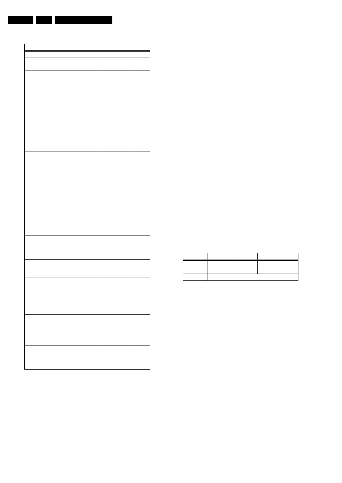
Table 5-3 NVM Default values (option bit settings through NVM Editor in SAM Mode)
Byte Nr. Bit Feature/Mode Description
Byte 0
174(dec)
Byte 1
175(dec)
Byte 2
176(dec)
Byte 3
177(dec)
Byte 4
178(dec)
Byte 5
179(dec)
0 QSS (LSB) Mode of quasi split sound amplifier 1
1 FMI Connection of output of QSS amplifier 1
2 HCO EHT tracking mode 0
3 HP2 Synchronization of OSD/Text display 1
4 FSL Forced slicing level for vertical sync 1
5 TFR DC transfer ratio of luminance signal 1
6 OSVE Black current measuring in overscan 0
7 MVK (MSB) (For Future Usage, as defined by software) 0
Total Dec Values 59
Total Hex Values 3B
0 PSE PSE 0
1OPC OPC 0
2 PRIS PRIS 0
3 CONTINUOUS FACTORY Continuous factory mode 1
4 WHITE PATTERN ON Last colour pattern status in factory mode 0
5 SDM MODE Service default mode on/off 0
6 SAM MODE Service Align mode on/off 0
7 SVMA Scavem On / Off 0
Total Dec Values 8
Total Hex Values 08
0 MUTE STATUS Mute status 0
1 TUNER AUTO MODE Auto mode 1
2 CABLE MODE Cable/Antenna mode 0
3 LAST POWER MODE Last power status of the set 1
4 CHILD LOCK MODE Child lock enabled 0
5 SURF MODE Surf mode on/off 0
6 FACTORY MODE Factory mode on 1
7 PSNS For PAL colour enhancement in ES4 1
Total Dec Values 202
Total Hex Values CA
0 RADIO/TV MODE Radio mode or TV mode 0
1 WAKE-UP MODE WAKE-UP MODE 0
2 HOTEL MODE TV in Hotel mode 0
3 HOTEL KBD LOCK Keyboard locked 0
4HBL HBL 0
5 BLS Blue stretch mode 1
6SL SL 0
7 CFA0 Comb filter On/Off 0
Total Dec Values 32
Total Hex Values 20
0 Signal Strength Signal Strength Switch in MK2 0
1LPG LPG 0
2 DVD TRAY LOCK Lock/Unlock DVD tray 0
3 SCRSAVER MODE Screen saver mode 1
4 BKS Black Stretch Mode 1
5 BSD Black Stretch Depth 1
6 CRA0 Coring on SVM 1
7 PIP QSS PIP QSS 0
Total Dec Values 120
Total Hex Values 78
0 FFI Fast Filter 0
1 NNR No red reduction during blue stretch 1
2 MUS NTSC matrix 1
3 GAM Gamma control 1
4 CBS Control sequence of beam current limiting 0
5 LLB Low level of beam current limiter 0
6 DSA Dynamic skin tone angle area 1
7 DSK Dynamic skin tone angle on/ off 0
Total Dec Values 78
Total Hex Values 4E
EN 19LC4.31E AA 5.
26PF5321/10/12
32PF5321/10/12
37PF5321/10/12
26PF7321/12
32PF7321/12
37PF7321/10/12
42PF5421/10
Page 20
EN 20 LC4.31E AA5.
Byte Nr. Bit Feature/Mode Description
Byte 6
180(dec)
Byte 7
181(dec)
Service Modes, Error Codes, and Fault Finding
26PF5321/10/12
32PF5321/10/12
37PF5321/10/12
26PF7321/12
32PF7321/12
37PF7321/10/12
0 LTI status LTI last status 0
1 Inc_Life_Time Inc_Life_Time 0
2 PC_Mode PC_Mode 0
3 HD_Mode HD_Mode 0
4 Tact_Switch Tact_Switch 0
5 Set_In_Special_Stby Set_In_Special_Stby 0
6 Hotel_OSDDisplay Hotel_OSDDisplay 0
7 Hotel_MonitorOut Hotel_MonitorOut 0
Total Dec Values 0
Total Hex Values 00
0 Hotel_IconMode Hotel_IconMode 0
1DBE DBE 1
2SD SD 0
3 Set_in_PC_Sleep_Mode Set_in_PC_Sleep_Mode 0
4 Reserved Reserved 1
5 Reserved Reserved 0
6 Reserved Reserved 0
7 Reserved Reserved 0
Total Dec Values 18
Total Hex Values 12
42PF5421/10
5.7.2 Load Default NVM Values
In case a blank NVM is placed or when the NVM content is
corrupted, default values can be downloaded into the NVM.
(For empty NVM replacement, short the SDM with a jumper
and apply the mains voltage. Remember to remove the jumper
after the reload is completed). After the default values are
downloaded, it will be possible to start up and to start aligning
the TV set. This is no longer initiated automatically; to initiate
the download the following action has to be performed:
1. Switch “off” the TV set by disconnecting the AC Power
plug.
2. Short circuit an SDM jumper (keep short-circuited).
3. Press P+ or Ch+ on the local keyboard (and keep it
pressed).
4. Switch on the TV set via the AC Power plug.
5. Keep pressing the P+/Ch+ button until the set has started
up and the SDM is shown.
Alternative method:
1. Go to SAM.
2. Select NVM Editor (not SC NVM Editor).
3. Select ADR (address) to 1 (dec).
4. Change the VAL (value) to 170 (dec).
5. Store the value.
6. Disconnect the mains plug and wait for a few seconds.
7. Reconnect the mains plug and wait until the set goes into
its standby mode (red LED lights up).
8. Restart the set.
5. Manually store a known channel and check if there is IF
output at Tuner pin 11.
6. Check the tuning DC voltage at pin 2 of the Tuner. The DC
voltage should vary according to the frequency/channel
being chosen.
7. If the tuning voltage is OK, check the tuner output, pin 11.
8. If it has no output, the Tuner may have a defect. Change
the Tuner.
Sound in Picture Problem for L' System (rolling horizontal lines)
1. Check whether AGC L' in SAM mode is set to 0.
2. If yes, align the set to correct value.
Required System is not Selected Correctly
Check whether a Service jumper (#4204 & 4205, 0805 size) is
present. If yes, remove it.
5.7.5 Video Processing
No Power
1. Check +12 V and 3V3 at position 1J02.
2. If no supply, first check the connector 1J02.
3. If the connector is correct, check the power supply board.
Power Supply is Correct, but no Green LED
1. Check if the connectors 1K00 are properly inserted.
2. If they are inserted correctly, check if the 3V3 is present.
5.7.3 Flash New Scaler Software
When you need to flash new scaler software, follow the
instructions in ComPair. Make sure you put the set in one of the
Service Modes, SDM/SAM/CSM, before you start flashing.
This reduces the risk of the set hanging during the flashing
procedure.
5.7.4 Tuner and IF
No Picture in RF Mode, but there is a Noise Raster
1. Check whether picture is present in AV. If not, go to Video
processing troubleshooting section.
2. If present, check if the Option settings are correct.
3. Check if all the supply voltages are present (3.3/5/8/12/33
V).
4. Check if the I
2
C lines are working correctly (3.3 V).
No Picture Display (blank screen with correct sound output)
1. Check whether the user menu is visible.
2. If the user menu is OK, activate teletext mode.
3. If teletext is OK, the problem is in the ADC (B18) &
Columbus 3D combfilter (B19), if present (depending on
model, see also paragraph “Teletext Path” in chapter 9).
4. If the user menu is not visible, check if the LCD panel
backlight is ON.
5. If the backlight is OFF, the problem is in the power supply
board or LCD panel. Also check pin 12 (LAMP_ON_OFF)
of 1J02. It should be HIGH during normal operation.
Note: For fault finding purposes, it is important to know the
following: in Pixel Plus and Digital Crystal Clear models, which
have an ADC (B18) and Columbus 3D combfilter (B19), the
digital input of the scaler is used for the digital video path
(Hercules output), whereas the analogue RGB input (analogue
Page 21

Service Modes, Error Codes, and Fault Finding
input of the scaler) is only used for teletext. This means that no
mixed mode (video plus teletext simultaneously) is possible. If
there is sound and teletext, but no video and user menu (blank
screen), the digital path (Hercules - ADC - Columbus - Scaler)
is faulty. If there is sound but no teletext, the back-end part
(Scaler - LCD panel) is faulty. In Crystal Clear models, which
do not have an ADC and Columbus, the RGB path (analogue
input of scaler) is used for both video and teletext.
No TV, but PC is Present
1. Check if Hsync_SDTV and Vsync_SDTV are present at pin
1 & pin13 of 7E03.
2. If they are present, check teletext output.
3. If there is no teletext output, the IC TDA150xx may be
defect.
5.7.6 Power Supply
Check Fuse
The power supply (various models are used) contains one fuse
near the AC input connector X002.
1. Check with power supply in “off” state by means of ohmic
measurement.
2. Fuse X102 may open in case of severe lightning strikes
and/or failures in the power supply.
3. Check the standby signal at pin 10 of X200. ON is HIGH,
OFF is LOW. During standby mode only the 3V3 is present
at pin 10.
EN 21LC4.31E AA 5.
Protections Concept on Power Supply Board (two models)
1. 12 V output (pin 8 of X200): Short-circuit protected by 2.5
A fuse X610. Over-voltage protection when output voltage
is more than 40% above nominal value.
2. Vaudio output (+18 or +24 V, depending on power
supply model used); (pin 1 of X200): Short-circuit proof
(+18 V version has 2.5 A fuse X660). Over voltage
protection when output voltage is more than 40% above
nominal value.
3. 3V3STBY output (pin 3&4 of X200): Short-circuit proof
with auto-restart. Over voltage protection when output
voltage is more than 40% above nominal value.
4. 24 V output (for inverter X520 & X530): Short-circuit
proof with auto-restart. Over voltage protection when
output voltage is more than 40% above nominal value.
Standby Mode
1. Apply a 12 ohm load resistor of sufficient power rating to all
outputs mentioned above (+12 V, +18/ 24 V, +3V3 and +24
V). Connect the STBY pin (pin 10 of X200) to logical “L”
(low), i.e. to GND.
2. Over an input voltage range of 90 V
to 276 VAC only the
AC
+3V3 STBY output shall be up.
Normal Mode:
1. Apply a 12 ohm load resistor of sufficient power rating to all
outputs mentioned above (+12 V, +18/ 24 V, +3V3 and +24
V). Connect the STBY pin (pin 10 of X200) to logical “H”
(high), i.e. to the +3V3 STBY output via a 2,2 k pull up
resistor.
2. Over an input voltage range of 90 V
to 276 VAC all
AC
outputs shall be up. The voltage on the +3V3 STBY output
shall be 3.3 V over the entire input voltage range. The
voltage on the big 400 V capacitor on the power supply
should also be 400 V ± 10%.
Page 22

EN 22 LC4.31E AA5.
Personal Notes:
Service Modes, Error Codes, and Fault Finding
E_06532_012.eps
131004
Page 23
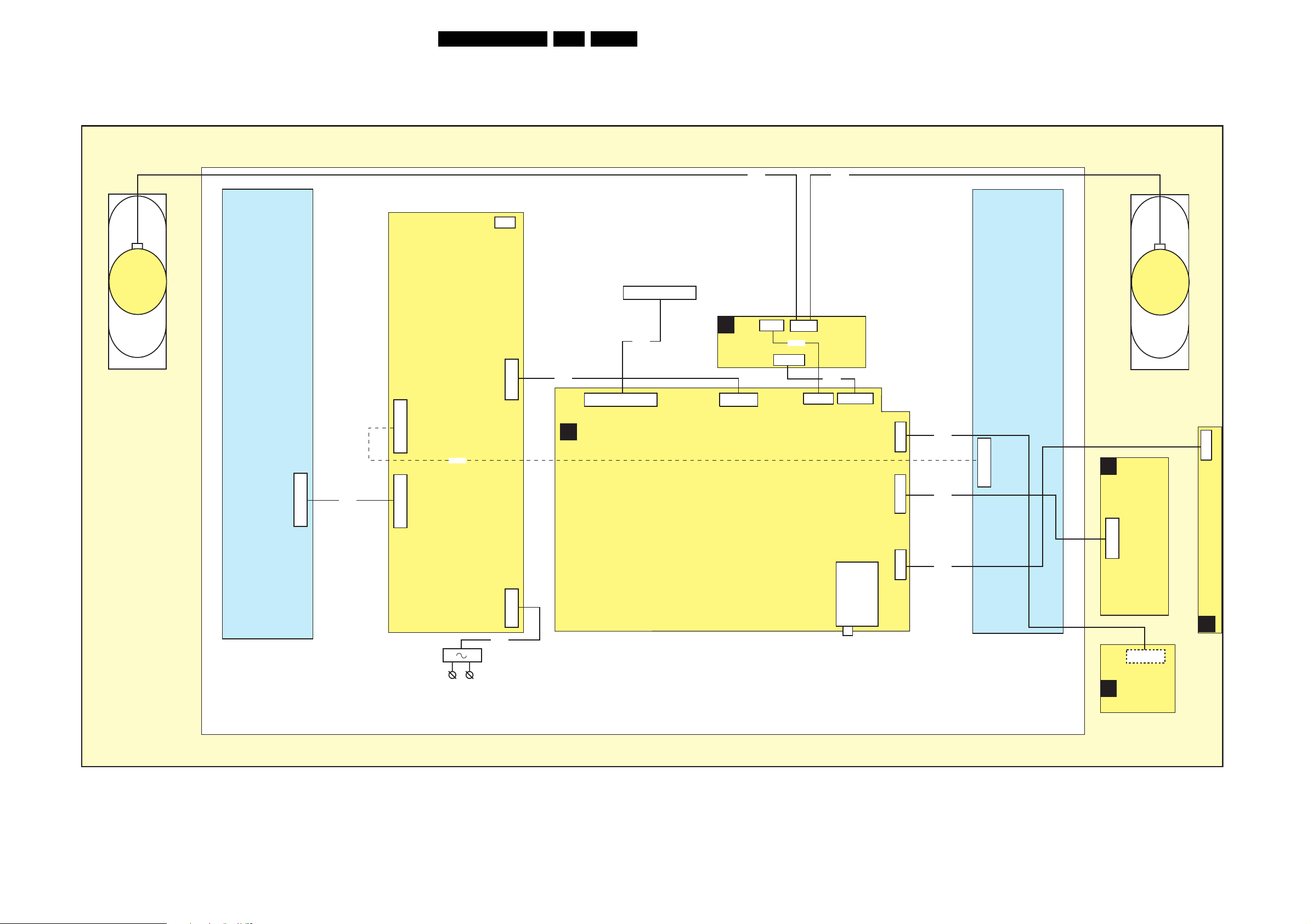
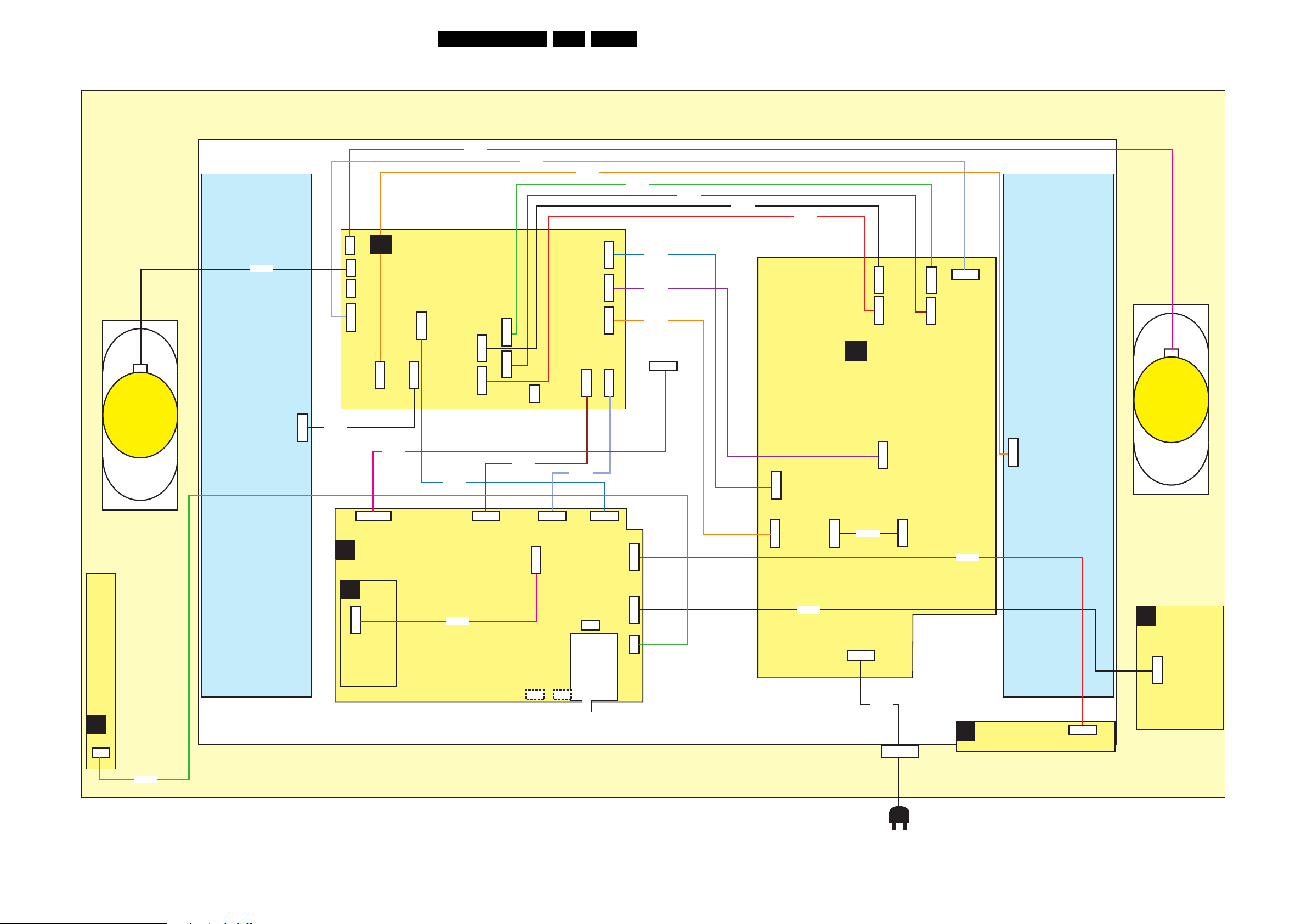
Block Diagrams, Test Point Overviews, and Waveforms
6. Block Diagrams, Test Point Overviews, and Waveforms
Wiring Diagram 26” & 32”
WIRING 26”- 32”
23LC4.31E AA 6.
RIGHT
SPEAKER
INVERTER
INVERTER
X530
X520
12P
POWER
SUPPLY
8520
3P
X220
X200
12P
8J02
B
SSB
LVDS CONNECTION
TO DISPLAY
30P
8P06
30P
31P
1P06
8903
C
CLASS D
AUDIO
AMPLIFIER
12P
1J02
1003
3P
1002
9P
8J03
4P
1001
3P
1J03
8903
8J04
1J04(1M52)
9P
6P
1K00(1M21)
8870
INVERTER
12P
D
LEFT
SPEAKER
SIDE AV
3P
1684
14P
8520
14P
AC POWER
INLET
POWER
IN
8002
X002
2P3
TUNER
12P
1K01(1M06)
3P
1K02
8K01
8684
12P
1304
IR/LED/LIGHT
J
SENSOR
(1M06)
6P
1870
G_16210_058.eps
010206
KEYBOARD CONTROL
E
Page 24
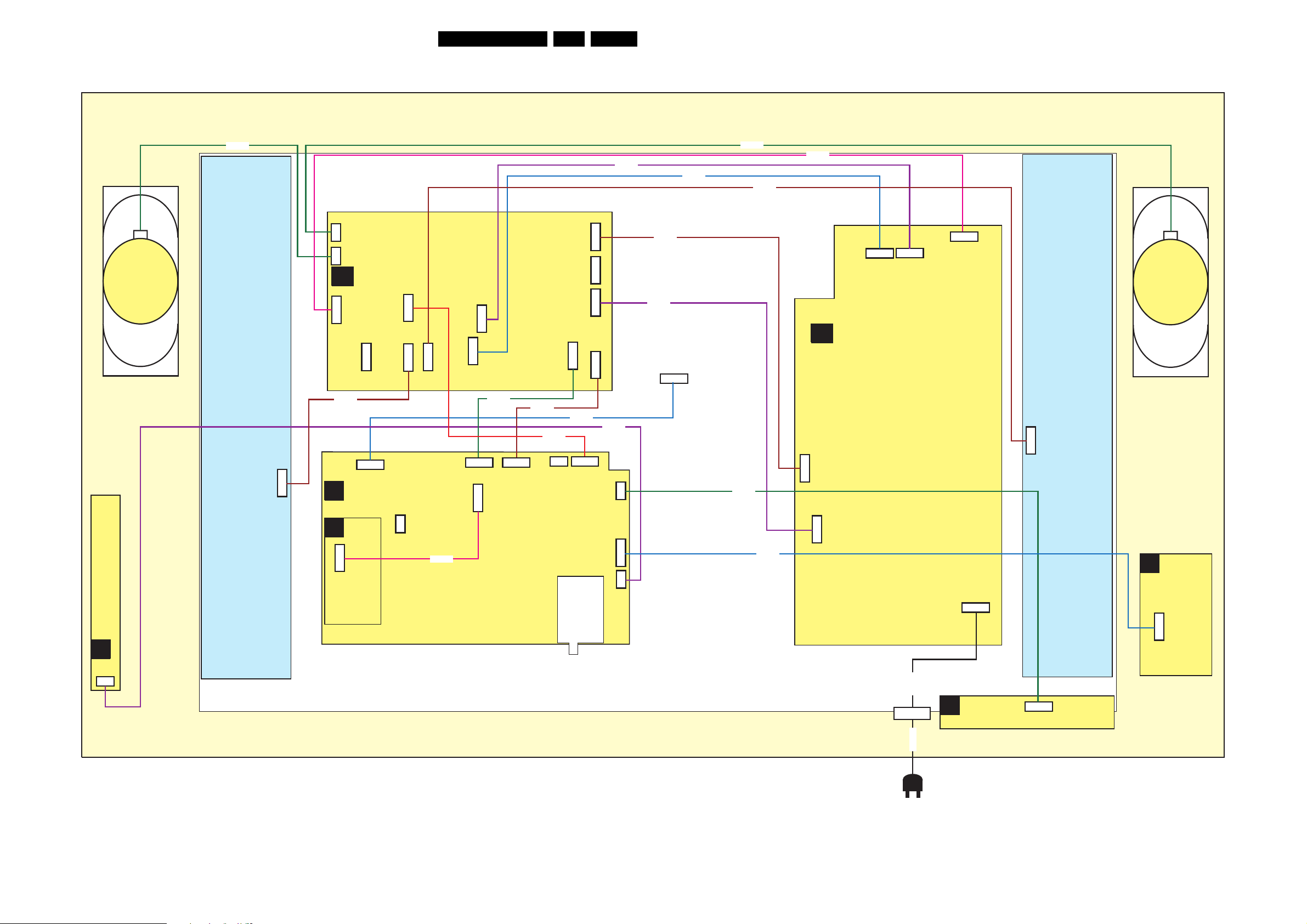
Block Diagrams, Test Point Overviews, and Waveforms
Wiring Diagram 37”
WIRING 37”
24LC4.31E AA 6.
RIGHT
SPEAKER
8902
INVERTER
14P
3P
3P
SA
7P
8521
B
1736
1735
STANDBY
1M02
12P
1316
30P
1N17
SSB
1739
9P
14P
1319
12P
1317
1309
11P
1J01
1442
1304
3P
14P
4P
8337
10P
1J00
8322
8J04
1J03
3P
1M46
8P06
11P
9P
1J04
1306
1307
1305
1M03
2P3
4P
3P
10P
8101
1K00
8304
6P
8309
LCD PANEL
8306
8305
TO DISPLAY
LV DS
8870
8903
8520
8302
LCD SUPPLY
A
2P3
1306
3P
1309
4P
1304
7P
1M02
LEFT
SPEAKER
INVERTER
12P
KEYBOARD CONTROL
E
1M01
3P
T
1000
OTCFLASH
14P
1N20
3P
8000
TUNER
1K04
1K02
11P
3P
8K01
3P
1305
8002
AC INLET
8187
J
(8188UK)
1308
2P3
LED PANEL
6P
0345
SIDE AV
D
11P
1M36
G_16210_059.eps
180506
Page 25
Block Diagrams, Test Point Overviews, and Waveforms
Wiring Diagram 42”
WIRING 42” LCD
RIGHT
SPEAKER
8735
INVERTER
14P
8319
2P3
2P3
2P3
7P
SA
1736
1735
1738
1M02
1316
8736
STANDBY / AUDIO
9P
1739
12P
1319
14P
1303
1320
4P
3P
1304
1309
4P
3P
8302
4P
1M10
8317
1M46
11P
25LC4.31E AA 6.
8304
2P3
1306
4P
1307
3P
1305
LCD PANEL
10P
1M03
8306
8307
8305
LV DS
30P
8309
8303
8320
4P
1303
3P
1320
MF + SUPPLY
A
4P
3P
1304
1309
7P
1M02
INVERTER
LEFT
SPEAKER
CONTROL BOARD
E
1M01
3P
B
T
1000
31P
1N17
SSB
OTCFLASH
14P
8150
8152
8000
11P
1J01(1M46)
8146
1177
UART
10P
1J00(1M03)
14P
1442
1151
3P
Compair
3P
8103
1J04(1M52)
1103
3P
Tuner
9P
6P
1K00(1M21)
11P
1K04(1M06)
3P
1K02
2P3
3P
1306
1B06
8136
1305
3P
1420
1308
2P
4P
8308
AC INLET
1307
3P
1C05
8120
LED SWITCH
J
PANEL
12P
6P
0345
D
SIDE I/O
11P
1M36
8101
G_16210_101.eps
190506
Page 26
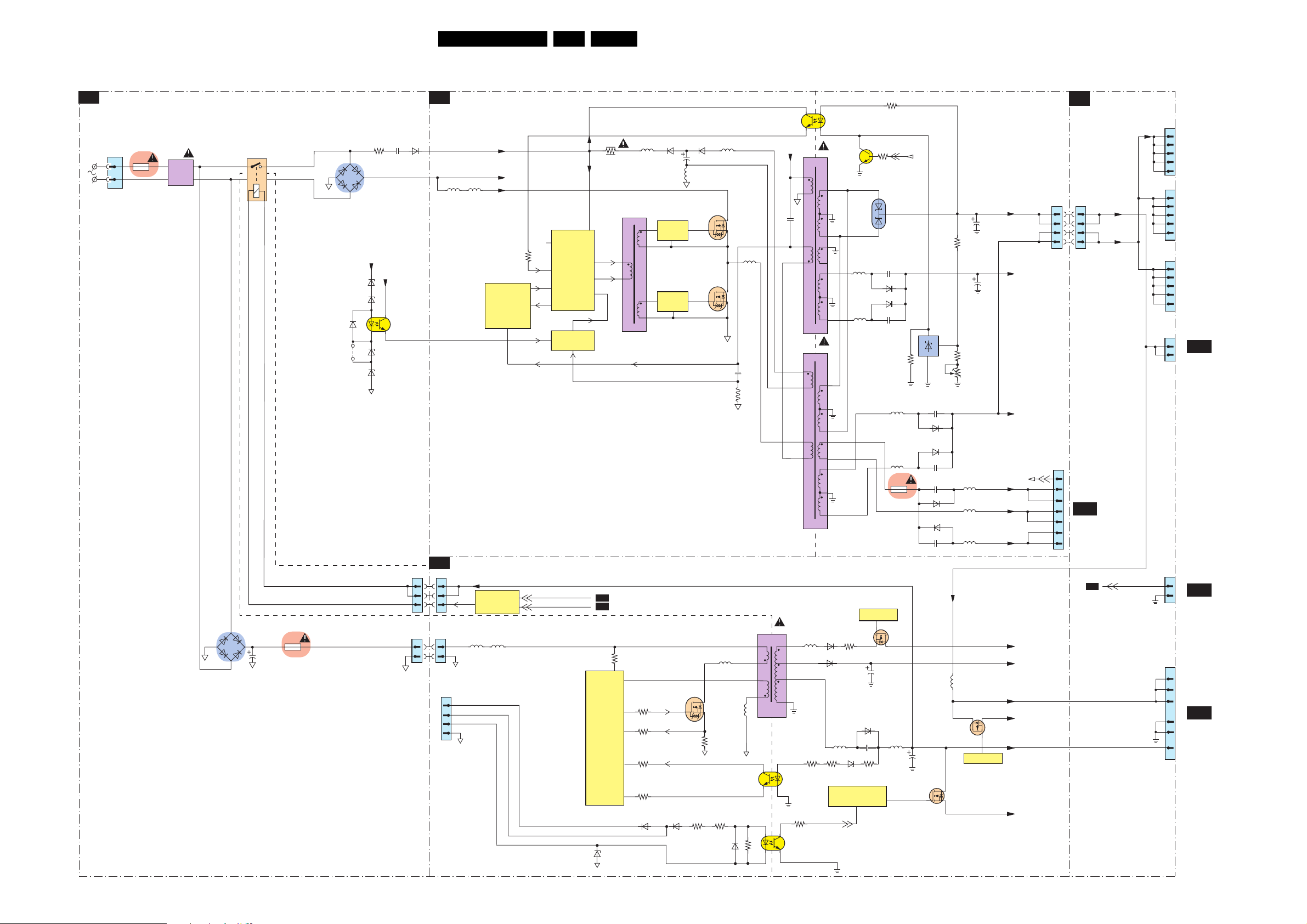
Block Diagrams, Test Point Overviews, and Waveforms
Block Diagram Supply 37”
SUPPLY 37"
MAINS FILTER + STANDBY
A1
1308
1314
2
T5AH
1
5305
5306
MAINS
FILTER
26LC4.31E AA 6.
400V_HOT
2059
HOT COLD
14
7002
TCET1102
2
3
5011
5002
5025
5026
7003
3057
3031
DC_PROT
6019
STPS20L40CFP
6019
STPS20L40CFP
2029
6021
6041
2045
5021
3030
7010
TS2431
2042
6031
3052
3025
2020
VS Voltage
Adj.
3026
2022
+12V
+24Va
+24Vb
1304
44
33
22
11
SUPPLY
A2
BIAS SUPPLY
VCC
3000
15
14
OA
12
OB
10
FI
5017
5001
4
2
7007
6
7
7008
10
9
2319
+
399V_HOT
6318
9311
3318
25V_HOT
6315
6316
14
2
6317
6314
1350
2
3
4
1
6307
GBJ6J
-
RES
7307
TCET1102
3
6304
5007
5008
25V_HOT
400V_HOT
399V_HOT
7011
7012
SOFT
START
+
CURRENT
PROTECTION
3007
7001
MC34067P
11
OSCC
7
ERROR
11
SOST
5
VREF
7004
7009
PROTECTION
CONTROL
OVER
VOLTAGE
HIGH
SIDE
DRIVE
LOW
SIDE
DRIVE
2003
5009
STP15NK50
STP15NK50
60246025
7005
7006
PRINTED
COMPONENT
5010
5012
2060
SA1
1304
CONNECTIONS
+12V_A
+12V_+24V
1316
1
2
3
4
5
1317
1
2
3
4
5
1319
1
2
3
4
5
1M10
1
2
(ONLY DVB SETS)
TO
DISPLAY
TO
DISPLAY
TO
DISPLAY
TO 1301
B01B
K3
IBO ZAPPER
6306
DF06M
-
6040
2512
2049
2009
6029
6030
2021
+12V_A
5507
STANDBY: LOW = ON
HIGH = STBY
7531
5020
5018
5019
7131
STANDBY
VSND_POS
GND_SND
VSND_NEG
RES
VTUN
+11V
+12V
+8V6
+5V2
+5V_SW
DC_PROT
1M02
7
6
5
TO 1M02
4
SA3
3
AUDI O
2
1
1M03
TO 1M03
1M46
010206
7
B01B
B16
4
SSB
11
9
4
TO 1M46
B01B
B16
1
SSB
2
7
SA2
STANDBY
G_16210_060.eps
5022
1007
T5A
5500
14
2
6
7
8
10
7501
TCET1102
3158
7150
TCET1102
3
HOT COLD
6504
5110
6140
3124
3128
PROT-OVV
7507
7506
7512
3509
5103
6122
OVERVO LTAGE
PROTECTION
STANDBY
6107
2513
3113
7511
RES
2141
5506
HOT
COLD
2303
1315
T1A
+
1305
1306
SA2
1305
11
22
33
1306
11
22
1307
1
2
N.C.
3
4
STANDBY
+5V2
5504
CONTROL
7505/7509/7560
5505
Prot-OVV
PROT_AUDIOSUPPLY
SA2
SA1
7100
7101
7105
CONTROL
6153
3101
3104
3150
3127
3100
6150
7102
STP15NK50
6151
3108
3155
5104
3V MAX
1V MAX STBY
3156
6156
COLD
HOT
5
3
2
1
5105
3157
HOT COLD
3
14
2
Page 27
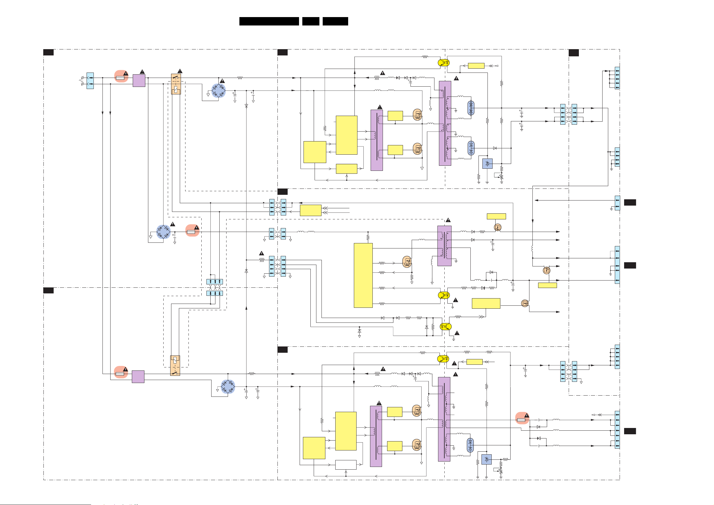
Block Diagrams, Test Point Overviews, and Waveforms
Block Diagram Supply 42”
SUPPLY 42"
MAINS FILTER + STANDBY PART A
A1
1308
MAINS INPUT
MAINS FILTER + STANDBY
A3
PAR T B
1
2
MAINS_L
MAINS_N
1400
3A15
1400
3A15
5400
5401
5403
MAINS
FILTER
5D00
5D01
5D03
MAINS
FILTER
6506
DF06M
27LC4.31E AA 6.
5010
5104
3U28
3028
5U105U17
5009
5040
5105
6156
5U09
5U40
HOT COLD
8
7
3
5
HOT COLD
COLD
HOT
5
3
2
1
14
3157
2
HOT COLD
8
7
3
5
HOT COLD
2143
5002
5500
2143
2143
5U02
7002
TCET1102
5027
9
10
11
12
13
5025
14
15
16
6
7
8
10
7501
TCET1102
3158
7150
TCET1102
3
7U02
TCET1102
9
10
11
12
13
5U25
14
15
5U26
16
5028
5026
5110
3128
3U57
7030
DC_PROT
6019
STPS20L40CFP
3
2
1
6021
STPS20L40CFP
1
2
3
6504
6140
5103
3124
OVERVO LTAGE
PROTECTION
PROT-OVV
DC_PROT
6021
STPS20L40CFP
1
2
3
3U30
3030
3509
6122
DC_PROT
3022
6021
STTH2003CFP
7010
TL431ACD
7507
7506
7512
STANDBY
6107
2513
3113
3U52
DC_PROT
3U39
3U22
7U10
TL431ACD
6014
2141
7511
3057
3052
3025
3U25
3026
5506
3U24
3U26
VS Voltage
Adj.
2512
VS Voltage
Adj.
2020
2022
7531
1U07
T5A
+12V
+24Va
+5V2-RELAY-IO2_PWM
N.C.
+12V_A
5507
7131
STANDBY
STANDBY: LOW = ON
HIGH = STBY
RES
+24V
2U22
2B91
6B91
6B93
2B93
VTUN
+11V
+12V
+8V6
RES
+5V2
+5V_SW
5B93
5B91
5B92
1304
44
33
22
11
1303
11
22
33
44
SA1
1304
1303
CONNECTIONS
+12V_A
+12V_+24V
+24V_2
VSND_POS
VSND_NEG
G_16210_102.eps
DC_PROT
1316
1M10
1M03
1M46
1317
1M02
190506
1
2
TO
3
DISPLAY
4
5
1
2
N.C.
3
4
TO 1M03
9
B01B
B16
4
SSB
11
9
TO 1M46
1
B01B
B16
2
SSB
7
1
2
TO
3
DISPLAY
4
5
7
6
5
SA3
TO 1M02
4
SA3
3
AUDIO
2
1
SUPPLY PART A
A2
1450
2
3
4
1
HOT
COLD
2503
14
1D50
3
1401
T1A
+
-
HOT
COLD
2
6807
GBJ6J
-
1B06
11
22
1C05
6H07
GBJ6J
+
33
+
-
3810
2815
China
6156
6157
400V_HOT_B
3H10
2H15
China
2816
3406
2H16
1305
11
22
33
1306
11
22
1307
11
22
33
44
25V_HOT_A
400V_HOT_A
SA2
1305
1306
1307
A4
25V_HOT_B
400V_HOT_B
7017
7018
CURRENT
PROTECTION
STANDBY
+5V2
CONTROL
7505/7509/7560/
5504
5505
SUPPLY PART B
7U17
7U18
START
CURRENT
PROTECTION
SOFT
START
SOFT
+
+
3U07
7001
MC34067P
11
OSCC
3007
7
ERROR
11
SOST
5
VREF
7004
7009
PROTECTION
Prot-OVV
PROT_AUDIOSUPPLY
7U01
MC34067P
11
OSCC
7
ERROR
11
SOST
5
VREF
7U04
7U09
PROTECTION
CONTROL
OVER
VOLTAGE
CONTROL
OVER
VOLTAGE
VCC
VCC
BIAS SUPPLY
15
14
OA
12
OB
10
FI
7100
7101
7105
CONTROL
6153
BIAS SUPPLY
15
14
OA
12
OB
10
FI
3101
3000
5007
5001
4
2
3U00
5U07
5U01
4
2
3104
3150
3127
3100
6150
6080
6077
6151
7102
6U79
6078
2003
7005
STP15NK50
STP15NK50
3V MAX
1V MAX STBY
3108
3155
6U77
7U05
STP15NK50
7U06
STP15NK50
7006
3156
6U78
2U03
5017
5008
7007
HIGH
6
SIDE
DRIVE
7
7008
LOW
10
SIDE
DRIVE
9
5U08
7U07
HIGH
6
SIDE
DRIVE
7
7U08
LOW
10
SIDE
DRIVE
9
Page 28
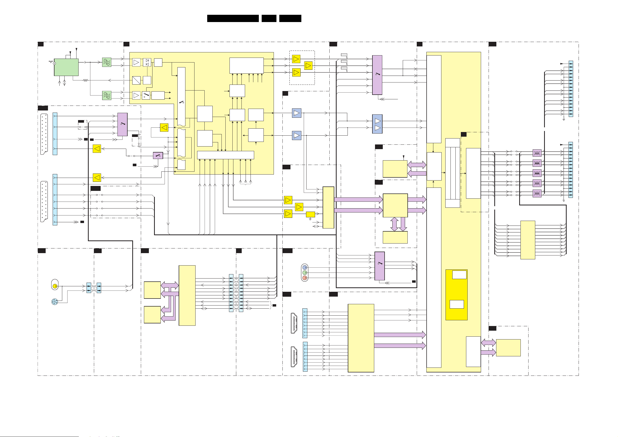
Block Diagrams, Test Point Overviews, and Waveforms
Block Diagram Video
VIDEO
TUNER & VIF
B1
RF
IN
SCART ANALOG IO
B15A
SCART 2
1
21
EXT 2
SCART 1
1
21
EXT 1
SIDE AV
D
(1002)
VIDEO
IN
(1001)
5
S-VHS
1152
UV1318S
1G02
20
15
8
19
1G01
19
20
16
15
11
1302
1301
1
2
SVHS
7
8
+5SW_a
67
TUNER
4
5
SCL
SDA
R
GB-R|YC-C_IN
STATUS_2_IN|OUT
SC1_CVBS
SC1_FB
CVI_Pr_IN
CVI_Y_
CVI_Pb_IN
STATUS_1
FRONT_YCVBS_IN
FRONT_C_IN
3
4
+VTUN
11
1
B15B
4G04
_IN
L_IN
IN
B2
( ) 37” - 42” only
2156
3154
B2
1304
(1M36)
IF-TER
FRONT
AV2_DMMI_SW
B2
7G05
EF
7G03
EF
B15B
B17
2
4
1154
1
1156
1
SC2_Y_IN
_Y_CVBS_IN
SC2_C_IN
FRONT_C_IN
DMMI
4G14
4G15
4G17
4G16
SIDE
CONNECTIONS
1K01
(1K04)
FRONT_YCVBS_IN
2
4
SC2_CVBS_MON_OUT
B2
7217
TDA15021H
4
VIF1
24
5
VIF2
25
31
RF_AGC
SIF1
29
4
30
SIF2
5
7G11
2
14
1
12
15
13
9
4G18
SC1_CVBS_RF_OUT
SC1_CVBS_IN
SC1_FBL_IN_1
SC1_CV1_DMMI_R_Pr_IN
SC1_CV1_DMMI_G_Y_IN
SC1_CV1_DMMI_B_Pb_IN
FRONT_C_IN
HERCULES
AC
DC
SC2_AV3_Y_IN
B15B
4G13
B7
SC2_OUT_SW
Sound
CVBS1
Tra p s
AGC
Detect
QSS/FM
QSS Mixer
AM
AM Demod.
SC2_AV3_C_IN
7206
EF
CVBS_COMB
SC2_Y_IN_1
7219
13
14
12
9
B2
B2,B13
B2,B13
B2,B13
CVBS_COMB
OTC-FLASH (FOR 1000pg TXT)
T
7007
MSM51V18165F
FLASH
ROM
512Kx8
7006
M29W160ET70N6E
FLASH
ROM
512Kx8
DD(0-15)
AA(1-20)
59
64
51
52
58
48
55
43
B3
Control
(OTC)
Video
Switch
+
c
cvbs/y
7001
SAA5801H/015
TV
CONTROL
HERCULES
Dig. 2H/4H
Combfilter
Y Delay Adj.
Chroma
PAL/NTSC/
SECAM
Decoder &
Baseband
Delay
INSSW3
R/Pr-3
G/Y3
77 78 79 80
Pr_IN
SC1_FBL_IN_1
SC1_CV1_DMMI_G_Y_IN
SC1_CV1_DMMI_R_
B15b
B15b
B15b
83
84
CVBS_COMB
5
96
79
74
78
79
77
78
INT_OTC
RESET_FLASH
(Only For 37” - 50” Sets)
Skin Tone
SAT
U/V Tint
Saturation
SCAVEM
Yint
Uint
Vint
RGB/Pr Pb Insert
YUV Interface
B/Pb-3
SC1_CV1_DMMI_B_Pb_IN
B15b
R_OTC
G_OTC
B_OTC
SCL
SDA
Peaking
on text
SCAVEM
U/V Delay
YOU T
VOUT
UOUT
74 75 76 70 71 72
1000
11
H
22
V
44
55
77
99
11 11
12 12
13 13
14 14
RGB Matrix
Blue & Black
Strech
Gamma Corr.
R_OSD
YUV
Vertical &
East-West
Geometry
YUV in/out
Sync Sep
H/V
VIN
UIN
YIN
N.C.
INTF_V_OUT
INTF_U_OUT
INTF_Y_OUT
SYNC INTERFACE
B3
(TO OTC-FLASH)
1442
CVBS_COMB
R_OTC_SDTV
G_OTC_SDTV
B_OTC_SDTV
RESET_FLASH
B_OSD
G_OSD
Fast Blanking
H-OSC
H-Shift
H-Drive
CVBS/Y
Hsync_SDTV
Vsync_SDTV
INT_OTC
SDA
SCL
RO
GO
BO
VDRB
HOUT
28LC4.31E AA 6.
MUX-SYNC INTERFACE
B13
7208
RO
85
GO
86
BO
87
22
VSYNC
HOUT
67
B13
B13
B2
B7
B13
B13
B13
B2
EF
7210
EF
For sets without
OTC-Flash (26”, 32”)
SYNC INTERFACE
B3
7436-2
7436-1
ADC
B18
7L61/7L62
EF
7L51/7L52
7L71
EF
SCART ANALOG IO
B15A
DIGITAL IO
B14
1
18 2
19
HDMI-1
1
18 2
19
HDMI-2
7209
EF
Vsync_SDTV
43
Hsync_SDTV
21
7L01
P3563M-LF
2
3
11
RX2+A
RX2-A
RX1+A
RX1-A
RX0+A
RX0-A
RXC+A
RXC-A
RX2+B
RX2-B
RX1+B
RX1-B
RX0+B
RX0-B
RXC+B
RXC-B
CONV.
6
9
37
38
EF
7L72
VIN VOUT
COM
SCL
SDA
1G01
1F02
1
3
4
6
7
9
10
12
1F03
1
3
4
6
7
9
10
12
B13
B13
B13
B3
B3
A/D
B15b
B15b
B15b
B12
FE00
R_OTC_SDTV
FE01
G_OTC_SDTV
FE02
B_OTC_SDTV
SC1_R_CVI_Pr_IN
SC1_G_CVI_Y_IN
SC1_B_CVI_Pb_IN
Vsync_SDTV
Hsync_SDTV
COL_Di(1-9)
COL_YA(1-9)
SC1_CV1_DMMI_R_Pr_IN
SC1_CV1_DMMI_G_Y_IN
SC1_CV1_DMMI_B_Pb_IN
GINA|YINA
HDMI
7D03
SII9993CTG100
A9
A10
A12
A13
PANELLINK
A15
RECEIVER
A16
F16
G16
C10
C9
C13
C12
C16
C15
G14
F14
BINA|Pb
RINA|Pr
HDMI
7E01
27
3
7
25
1
5
7604
5
1
13
12
1
3
5
2
9
B10
B19
7E00
A2
A1
D1
R-PR-ADC
17
G-Y-ADC
14
B-PB-ADC
11
I_PC_HD_SEL
8
4
SDRAM
7B01
K4D263238F
SDRAM
1Mx32x4
COLUMBUS
(Dig. PAL/NTC Comb)
7M00
T6TU5XBG
COLUMBUS
DIGITAL COMB
FILTER
7M01
MSM56V16
DRAM
512Kx16x2
SC1_R_CVI_Pr_IN
14
SC1_G_CVI_Y_IN
15
SC1_B_CVI_Pb_IN
4
RGB|CVI_HDA_SEL
9
+2V5_DDR
COL_A
H_HDMI
V_HDMI
HDMI_VCLK
HDMI_Y(0-7)
HDMI_CbCr(1-7)
R_PR+
G_Y+
B_PB+
AVSY NC
AHSYNC
95
COL_DQ
B7
SOG
FSDATA
FSADDR
COL_Do(1-8)
COL_YB(1-8)
B7
B13
B13
B13
SCALER
7801
GM1501
C3
D2
C2
B2
L3
L4
C14
B14
D16
ANALOG
INPUT
PORT
FRAME
STORE
CONTROL
DVI/HDMI
INPUT
PORT
SCALER
GRAPHIC
ZOOM
OUT BLENDER
OSD CONTROLLER
BRIGHTNESS/CONTRAST/HUE/SAT
VIDEO
ZOOM
UART
INTERFACE
MICRO
CONTROLLER
INTERNAL
RAM
B9
SCALER
DISPLAY
TIMING
GEN.
EXTERNAL
ROM
INTERFACE
AE16
AF16
AE15
AF15
AE14
AF14
AF12
AF11
AF13
AE12
OCMADDR
B20
B11
OCMDATA
PAC IF IC 3
TXB0TXB0+
TXB1TXB1+
TXB2TXB2+
TXB3TXB3+
TXBCTXBC+
OR
TXB0+
TXB0TXB1+
TXB1TXB2+
TXB2TXB3+
TXB3TXBC+
TXBC-
FLASH/CONTROL
7C03
M29W400DT55N6E
FLASH
ROM
512Kx8
4N02
4N01
4N04
4N03
4N06
4N05
4N10
4N09
4N08
4N07
29
28
32
31
35
34
41
40
37
38
1N12
TXO0TXO0+
1N13
TXO1TXO1+
1N14
TXO2TXO2+
1N15
TXO3TXO3+
1N11
TXOCTXOC+
7N00
T6TF4AFG
LVD S
PACIFIC3
(RES For PIXEL+)
1N16
LVDS_VCC
LVDSALVD S A+
LVD S BLVD S B+
LVDSCLVD S C+
LVDSDLVD S D+
LVDSCLKLVDSCLK+
OR
LVDS_VCC
LVD S ALVD S A+
LVD S BLVD S B+
LVD S CLVD S C+
LVD S DLVD S D+
LVDSCLKLVDSCLK+
TXO0-
103
TXO0+
102
TXO1-
101
TXO1+
100
TXO2-
99
TXO2+
98
TXO3-
93
TXO3+
92
TXOC-
96
TXOC+
95
1
11
12
13
14
15
16
17
18
19
20
24
25
26
21
22
1N17
1
11
10
12
14
13
15
19
18
20
27
26
28
22
21
23
G_16210_061.eps
070206
TO DISPLAY (26” & 32”)TO DISPLAY (LCD 37” & 42”, PDP 42” & 50”)
Page 29
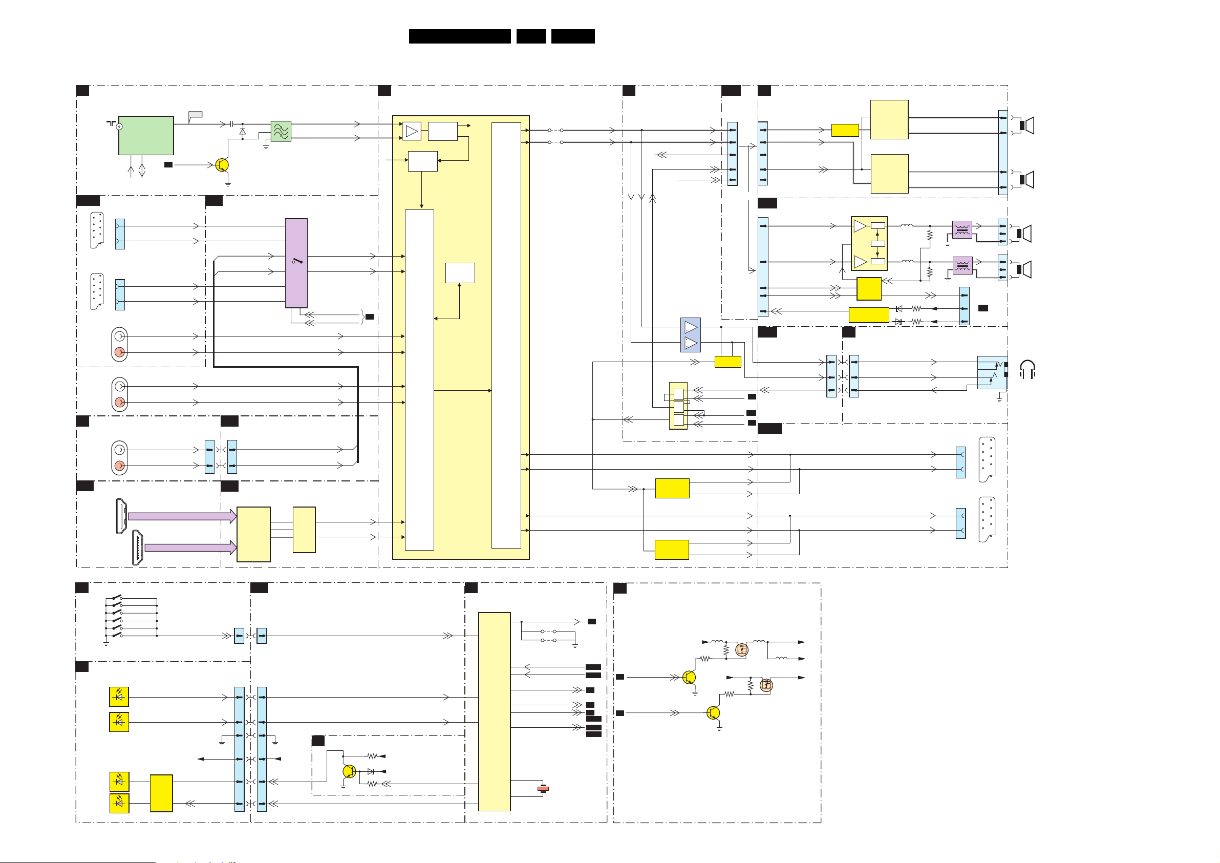
Block Diagrams, Test Point Overviews, and Waveforms
Block Diagram Audio
AUDIO
TUNER & IF
B1
1152
UV1318S
RF IN
SCART ANALOG-IO
B15A
1G01-1
1
6
2
21
EXT 1
SCART 1
1G02-1
1
6
2
21
EXT 2
SCART 2
1G02-2
AUDI O
L/R IN
1F01
AUDI O
L/R IN
SIDE AV
D
B14
AUDI O
L/R IN
DIGITAL IO
HDMI 1
HDMI 2
1302
(1002)
1F02
1
18 2
19
CONTROL
KEYBOARD CONTROL
E
Channel+
Channel-
Menu
Vol ume +
Vol ume -
Power
IR/LED/LIGHT-SENSOR
J
REMOTE
CONTROL
LIGHT
SENSOR
LED
GREEN
LED
RED
1309(1703)
1310(1704)
3324(1705)
1311(1701)
1312(1702)
1313(1706)
TUNER
4
5
SCL
SDA
AV1_Audio_INL
AV1_Audio_INR
AV2_Audio_INL
AV2_Audio_INR
HD_AudioINL
HD_AudioINR
DVI_D_AudioINL
DVI_D_AudioINR
1F03
1
18 2
19
IFOUT
B2
L_FRONT_IN
R_FRONT_IN
( ) For 37” - 42”
LED
SELECT
11
SEL_IF_SDM
HDMI_A
HDMI_B
LIGHT-SENSOR
F158
IF-TER
B14
1304
(1M36)
KEYBOARD
RC
+3V3STBY
LED_SEL
PC-TV-LED
( ) For 37” - 42”
2156
7151
DIGITAL IO
SIDE_AudioINL
SIDE_AudioINR
B17
1K01
(1K04)
66
88
B12
7D03
TDA9975
1684
(1M01)
( ) For 37” - 42”
1870
(0345)
1156
4
1
2
6154
3
7F03
1
12
4
11
2
15
10
DVI_D_AudioINL
DVI_D_AudioINR
SIDE CONNECTORS
HDMI
HDMI
A5
1
A7
10-BIT
VIDEO
CONVERTER
B17
1K02
(1M01)
22
1K00
33
11
22
55
44
66
3
B7
2
SIDE CONNECTORS
+3V3STBY
LED_SEL
PC-TV-LED
5
3
13
9
Analog_AudioSEL1
Analog_AudioSEL2
HD_AudioINL
HD_AudioINR
SIDE_AudioINL
SIDE_AudioINR
7D04
UDA1334ATS
DAC
14
16
B3
SIF1
SIF2
Analog_AudioINL
Analog_AudioINR
B7
HDMI_AudioINL
HDMI_AudioINR
LSIPDP_DVB_SEMISTANDBY
SYNC INTERFACE
3431
7430
6430
3432
RES
HERCULES
B2
7217
TDA15021H
29
30
AD Conv.
33
Std Stereo
Decoder
34
35
49
AUDI O
50
SELECT
ADC/DAC
56
57
53
54
KEYBOARD
RC_OUT
+3v3STBY
+5VSW
P50_LIN2_ITV_IR_SW_RST
QSS Mixer
AM Demod.
Processor
AM
QSS/FM
I2S
B2
120
97
115
123
107
7217
TDA15021H
AUDI O
CONTROL
Vol /Tre b/
Bass
Features
DACs
HERCULES
HERCULES
114
116
119
102
111
122
127
10
11
4211
61
4212
60
62
63
36
37
SEL_IF_SDM
4204
4205
SERVICE
SDM
STATUS_1
STATUS_2
EXT_MUTE
SOUND-ENABLE
SC_STANDBY
AV2_DMMI_SW
1202
24M576
29LC4.31E AA 6.
AUDOUTLSR
AUDOUTLSL
OUT_MUTE
B1
B15A
B15A
B5
B5
B6
B15B
B15A
B15B
AUDIO PROCESSING
B5
OUT_MUTE
OUT_MUTE
7202
7201
DC-DC CONVERTER
B6
PANEL-PWR-CTL
B8
SC_STANDBY
B2
AUDI O-R
AUDI O-L
PROTECT_AUD
SOUND-ENABLE
POR_AUDIO
7601
TS482ID
2
6
7602
74HC08PW
2
3
&
1
&
6
5
9
8
&
10
MUTE
MUTE
+12VSW
7755
B16
1J04
1
7
7606
MUTE
HP_DET_R_DC_1
SOUND_ENABLE
POWER_DOWN
EXT_MUTE
SC2_L_MON_OUT
SC2_R_MON_OUT
SC2_L
SC2_R
SC1_L_RF_OUT
SC1_R_RF_OUT
SC1_L
SC1_R
5756 5757
3758
3755
+3V3STBY
3759
7756
AUDIO AMPLIFIER
C
(CLASS-D)
1002
33
11
77
88
99
OR
SOUND-ENABLE
FOR 26” & 32” ONLY
SA3
1739
1
3
8
9
7
FOR 37”ONLY
B17
HP_DET_R_DC_1
B2
B16
B2
B15A
7754
5700
7758
3750
AUDI O-R
AUDIO-L
AUDI O
AUDI O-L
AUDI O-R
SOUND-ENABLE
POR-CLASSD
PROT_AUDIOSUPPLY
SIDE
CONNECTORS
HP_LOUT
HP_ROUT
1K01
(1K04)
10 10
12 12
11 11
SCART ANALOG-IO
PAN_VCC
LVDS_VCC
+3V3SW
7004
PHASE
INVERTER
10
6
18
D
(1M36)
7001
TDA8931T
COMPARATO R
7
4
IN+
7000
TDA8931T
COMPARATOR
7
4
IN+
7700
TDA7490
PWM
stby-
OSC
mute
PWM
7701÷7707
SOUND
ENABLE
7708÷7711
AUDIO SUPPLY
PROT, CIRCUIT
SIDE AV
1304
POWER
16
OUT
13
HVPI
POWER
16
OUT
13
HVPI
5702
3
5701
23
PROT1
DCPROT
6703
3764
6702
3761
HEAD_PH_L
HEAD_PH_R
HP_DET_R_DC1
SC2_L_MON_OUT
SC2_R_MON_OUT
SC1_L_RF_OUT
SC1_R_RF_OUT
3717
3718
-16 V-19V
+16 V+19V
5731
5730
1M02
1G02-1
3
1
1G01-1
3
1
7
TO 1M02
1
A
SUPPLY
5
1303
(1010)
7
1
2
( ) For 37” - 42”
EXT 2
SCART 2
EXT 1
SCART 1
1001
4
3
RIGHT
SPEAKER
2
1
SPEAKER
1736
1
2
3
1735
SPEAKER
1
2
3
SPEAKER
HEADPHONE
1
21
1
21
G_16210_062.eps
LEFT
LEFT
RIGHT
030206
Page 30
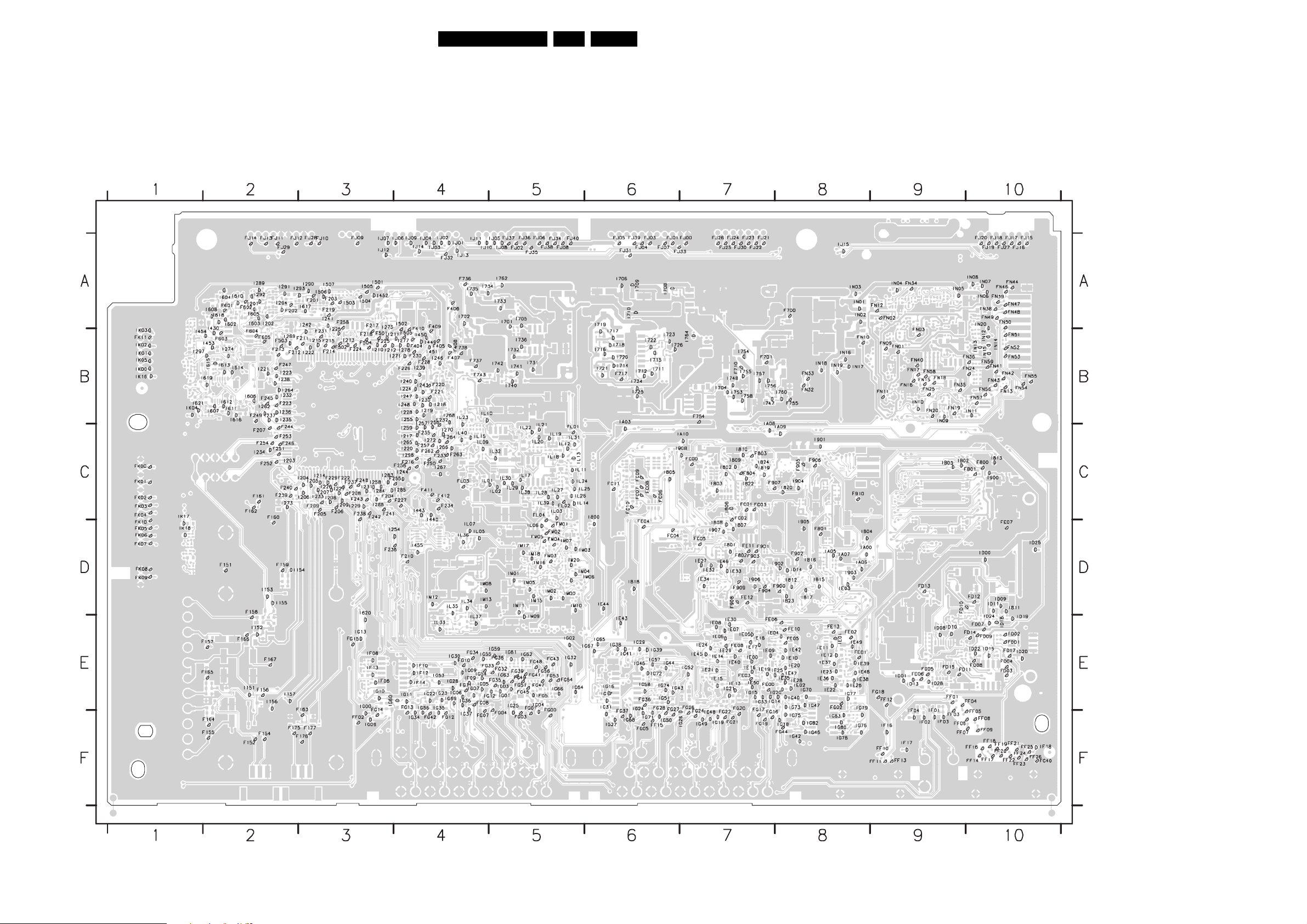
Block Diagrams, Test Point Overviews, and Waveforms
Test Point Overview Small Signal Board
F151 D2
F166 E2
F210 D4
F224 B3
F238 C3
F252 C2
F152 F2
F167 E2
F175 F2
F176 F3
F177 F3
F201 A3
F202 A2
F203 A3
F204 C3
F205 C3
F206 C3
F207 C2
F208 C3
F209 C3
F211 B3
F212 B2
F213 B2
F214 B3
F215 B3
F216 C4
F217 A3
F218 B3
F219 A3
F220 B4
F221 B4
F222 C3
F223 B2
F154 F2
F155 F2
F156 E2
F157 E2
F158 D2
F159 D2
F160 C2
F161 C2
F162 C2
F163 E3
F164 F2
F165 E2
3139 123 6117.2
F225 B3
F226 B4
F227 C4
F228 B4
F229 C3
F230 B4
F231 B3
F232 B4
F233 C4
F234 C4
F235 C4
F236 D3
F237 C3
F239 C2
F240 C2
F241 C3
F242 C3
F243 C3
F244 C2
F245 B2
F246 C2
F247 B2
F248 C3
F249 B2
F250 C4
F251 C2
F253 C2
F254 C2
F255 C4
F256 C4
F257 C4
F258 A3
F262 C4
F263 C4
F264 C4
F404 B4
F405 B4
F406 A4
F407 B4
F408 B4
F409 A4
F410 B4
F411 C4
F412 C4
F501 B3
F502 B3
F503 B2
F504 B3
F505 B4
F601 A2
F602 A2
F603 B2
F604 B2
F605 B2
F700 A8
F701 B7
F710 B7
F717 B6
F736 A4
F737 B4
F738 B4
F743 B4
F754 B7
F755 B8
F800 C10
F801 D8
F802 D7
F803 C7
F804 C7
F900 D8
F901 D7
F902 D8
F903 D7
F904 D7
F905 C8
F906 C8
F907 C7
F908 D7
F909 D7
F910 C8
FB01 C10
FC00 C7
FC01 C7
FC02 C7
FC03 C7
FC04 D6
FC05 D7
FC06 C6
FC07 C6
FC08 C6
FC09 C6
FC10 C6
FC11 C6
FD01 E10
FD02 E10
FD03 E10
FD04 E10
FD05 E9
FD06 E9
FD07 E10
FD08 E10
FD09 E10
FD10 D9
FD11 E9
FD12 D10
FD13 D9
FD14 E10
FD15 E9
FD17 E10
FE00 E7
FE01 E8
FE02 E8
FE03 E7
FE04 D6
FE05 E8
FE06 E7
FE07 D10
FE08 E7
FE10 E8
FE11 D7
FE12 D7
FE13 E8
FF01 E9
FF02 F3
FF03 F9
FF04 E10
FF05 F10
FF06 F9
FF07 F9
FF08 F10
FF09 F10
FF10 F9
FF11 F9
FF12 E9
FF13 F9
FF14 F10
FF15 F6
FF16 F10
FF17 F10
FF18 F10
FF19 F10
FF20 F10
FF21 F10
FF22 F10
FF23 F10
FF24 F10
FF25 F10
FF26 F10
FG00 E5
FG01 E5
FG02 E8
FG03 F5
FG04 F5
FG05 F6
FG07 F4
FG08 E4
FG10 E4
FG11 E4
FG12 F4
FG13 E4
FG14 E3
FG15 E3
FG16 F7
FG17 E7
FG18 E9
FG19 F7
FG20 E7
FG21 F7
FG22 F7
FG24 F7
FG26 E7
FG27 E6
FG28 E6
FG32 E5
FG33 E4
FG34 E4
FG35 E5
FG36 E6
FG37 F6
30LC4.31E AA 6.
FG38 E5
FG39 E5
FG40 F10
FG41 E5
FG42 F4
FG43 E5
FG44 F8
FG45 E5
FG47 E5
FG48 E5
FG49 E5
FG51 E5
FG53 E5
FG54 E5
FG56 E5
FJ00 A7
FJ01 A6
FJ02 A5
FJ03 A6
FJ04 A6
FJ05 A6
FJ06 A5
FJ07 A6
FJ08 A5
FJ09 A3
FJ10 A3
FJ11 A2
FJ12 A2
FJ13 A2
FJ14 A2
FJ15 A10
FJ16 A10
FJ17 A10
FJ18 A10
FJ19 A10
FJ20 A10
FJ21 A7
FJ22 A7
FJ23 A7
FJ24 A7
FJ25 A7
FJ26 A7
FJ27 A10
FJ28 A3
FJ29 A2
FJ30 A7
FJ31 A6
FJ32 A4
FJ33 A7
FJ34 A5
FJ35 A5
FJ36 A5
FJ37 A5
FJ38 A5
FJ39 A6
FJ40 A5
FK00 C1
FK01 C1
FK02 C1
FK03 C1
FK04 C1
FK05 D1
FK06 D1
FK07 D1
FK08 D1
FK09 D1
FK10 D1
FK11 B1
FL01 C5
FL02 C5
FL03 C4
FL04 C5
FM01 D5
FM02 D5
FM03 D5
FM04 D5
FM05 D5
FN01 B9
FN02 A9
FN03 B9
FN09 B9
FN10 B8
FN11 B9
FN12 A9
FN13 B10
FN15 B9
FN16 B9
FN17 B9
FN18 B9
FN19 B9
FN20 B9
FN24 B10
FN25 B9
FN32 B8
FN33 B8
FN34 A9
FN35 B9
FN36 B10
FN38 A10
FN39 A10
FN40 B9
FN41 B10
FN42 B10
FN43 B10
FN44 A10
FN46 A10
FN47 A10
FN48 A10
FN49 A10
FN50 A10
FN51 B10
FN52 B10
FN53 B10
FN54 B10
FN55 B10
FN56 B10
FN57 B10
FN58 B9
FN59 B10
I151 E2
I152 E2
I153 D2
I154 D3
I155 D2
I156 E2
I157 E2
I201 A2
I202 A2
I203 C2
I204 C3
I205 C3
I206 C3
I207 C3
I208 C3
I209 C3
I210 B3
I211 B3
I212 B3
I213 B3
I214 C3
I215 B3
I217 C4
I218 B4
I219 B4
I220 C4
I221 B2
I222 B3
I223 B2
I224 B4
I225 B3
I226 C3
I227 C3
I228 B4
I229 C3
I230 B4
I231 C3
I232 B2
I233 C3
I234 C2
I235 B2
I236 B2
I237 B2
I238 B2
I239 B4
I240 B4
I241 A3
I242 A3
I243 B4
I244 C4
I246 B4
I247 B4
I248 B4
I254 D4
I255 B4
I256 B4
I257 B4
I258 C3
I259 C4
I262 B2
I264 B2
I265 C4
I266 C4
I267 C4
I268 B4
I269 B2
I270 C4
I271 B4
I272 C4
I273 C2
I274 B2
I275 A3
I277 B4
I278 B4
I283 C3
I284 C3
I285 C4
G_16210_024.eps
170106
I288 C3
I289 A2
I290 A3
I291 A2
I292 A2
I293 A3
I294 A2
I297 B1
I298 C4
I430 A2
I440 D4
I443 C4
I449 B4
I450 B4
I451 B4
I452 A3
I453 B2
I454 B1
I455 D4
I501 A3
I502 A4
I503 A3
I504 A3
I505 A3
I506 A3
I507 A3
I602 A2
I603 A2
I604 A2
I605 A2
I606 B2
I607 B2
I608 A2
I610 A2
I611 B2
I612 B2
I613 B2
I614 B2
I615 B2
I616 B2
I617 A3
I618 A2
I619 B2
I620 D3
I621 B1
I701 A5
I702 A4
I704 B7
I705 A5
I706 A6
I708 A6
I709 A6
I710 A6
I711 B6
I712 B6
I714 B6
I715 B6
I716 B6
I717 B6
I718 B6
I719 A6
I720 B6
I721 B6
I722 B6
I723 B6
I724 B6
I725 B6
I726 B6
I731 B5
I732 B5
I733 A5
I734 A4
I735 A4
I736 B5
I740 B5
I741 B5
I742 B5
I747 B7
I748 B7
I753 B7
I754 B7
I755 B7
I756 B7
I757 B7
I758 B7
I760 B8
I762 A5
I764 B7
I800 C6
I801 D7
I802 C7
I803 C7
I804 D8
I805 C6
I806 C7
I807 D7
I808 D7
I809 C7
I810 C7
I811 D10
I812 D8
I813 C10
I815 D8
I816 D8
I817 D8
I818 D6
I819 C7
I820 C8
I822 C7
I823 D8
I824 C7
I900 C10
I901 C8
I902 D8
I903 D8
I904 C8
I905 D8
I906 D7
I907 D7
I908 C7
IA00 D8
IA03 B6
IA05 D8
IA06 D8
IA07 D8
IA08 B7
IA09 C8
IA10 C7
IB02 C9
IB03 C9
ID00 D10
ID01 E9
ID08 E9
ID09 D10
ID10 E9
ID11 D10
ID13 E9
ID14 D8
ID15 E10
ID18 E10
ID19 E10
ID20 E10
ID22 E10
ID24 E10
ID25 D10
ID28 E9
IE00 E7
IE01 E8
IE02 E8
IE03 D8
IE04 E7
IE05 E7
IE06 E7
IE07 E7
IE08 E7
IE09 E7
IE10 E8
IE11 E8
IE12 E8
IE13 E7
IE14 E7
IE15 E7
IE16 E7
IE17 E7
IE18 E7
IE19 E7
IE20 E8
IE21 E7
IE22 E8
IE23 E8
IE24 E7
IE25 E8
IE26 E8
IE27 D7
IE28 E8
IE29 E7
IE30 E7
IE32 D7
IE33 D7
IE34 D7
IE35 E8
IE36 E8
IE37 E8
IE38 E8
IE39 E8
IE40 E7
IE42 E8
IE43 E6
IE44 D6
IE45 E7
IE46 D7
IE47 E8
IE48 E8
IE49 E8
IE50 E7
IF01 E9
IF02 F9
IF03 F9
IF04 F9
IF05 E5
IF06 E3
IF08 E3
IF09 E4
IF10 E4
IF12 E4
IF13 E3
IF14 E4
IF16 F9
IF17 F9
IF18 F10
IG00 E3
IG01 E5
IG02 E5
IG03 E5
IG04 E5
IG05 E4
IG06 E4
IG07 E4
IG08 F3
IG09 E4
IG10 E3
IG11 E4
IG12 E5
IG13 E3
IG14 E7
IG15 E7
IG16 E6
IG17 E6
IG18 F8
IG19 F7
IG20 E8
IG21 E7
IG22 E4
IG23 E4
IG24 E6
IG25 E5
IG26 F7
IG27 F6
IG28 E4
IG29 E6
IG30 E4
IG31 E6
IG32 E5
IG33 E7
IG34 F4
IG35 E4
IG36 E4
IG37 F4
IG38 E6
IG39 E6
IG40 E8
IG41 E6
IG42 F8
IG43 E6
IG44 E6
IG45 E6
IG46 F8
IG47 E8
IG48 F7
IG49 F7
IG50 F6
IG51 E6
IG52 E7
IG53 E4
IG54 E4
IG55 E4
IG56 E4
IG57 E6
IG58 E6
IG59 E5
IG60 E3
IG61 E5
IG62 E5
IG63 E5
IG64 E5
IG65 E6
IG66 E5
IG67 E6
IG68 F6
IG69 E4
IG70 E8
IG71 F6
IG72 E6
IG73 E8
IG74 E6
IG75 F8
IG76 F8
IG77 E8
IG78 F8
IG79 E8
IG80 F8
IG82 F8
IG83 F8
IJ01 A4
IJ02 A4
IJ03 A4
IJ04 A4
IJ05 A5
IJ06 A4
IJ07 A3
IJ08 A5
IJ09 A4
IJ10 A4
IJ11 A4
IJ12 A3
IJ13 A4
IJ14 A4
IJ15 A8
IK00 B1
IK01 B1
IK02 B1
IK03 B1
IK04 B1
IK05 B1
IK16 B1
IK17 C1
IK18 D1
IL01 C4
IL02 C5
IL03 C5
IL05 D4
IL06 D5
IL07 D4
IL09 C4
IL10 B4
IL11 C5
IL12 C5
IL13 C5
IL14 C5
IL15 C4
IL17 C5
IL18 C5
IL19 C5
IL20 C5
IL21 C5
IL22 C5
IL23 B4
IL24 C5
IL25 C5
IL26 C5
IL27 C5
IL28 C5
IL29 C5
IL30 C5
IL31 C5
IL32 C5
IL33 E4
IL34 D4
IL35 D4
IL36 D4
IL37 E4
IL38 C5
IL39 C5
IL40 C4
IM00 D5
IM01 D5
IM02 D5
IM03 D6
IM04 D5
IM05 D5
IM06 D6
IM07 D5
IM08 D4
IM09 E5
IM10 D5
IM11 D5
IM12 D4
IM13 D4
IM15 D5
IM16 D5
IM17 D5
IM18 D5
IM20 D5
IN01 A8
IN02 A8
IN03 A8
IN04 A9
IN05 A9
IN06 A10
IN07 A10
IN08 A10
IN09 B9
IN10 B9
IN11 B10
IN12 B10
IN13 B10
IN14 B10
IN15 B10
IN16 B8
IN17 B8
IN18 B8
IN19 B8
IN20 A10
Page 31

I2C Overview
I²C
HERCULES
B2
Block Diagrams, Test Point Overviews, and Waveforms
7217
TDA15021H
HERCULES
SET
PROCESSOR
109
108
ERR
6
NVM_WP_HERC
104
122
112
113
+3V3STBY
3232
3233
+3V3STBY
3249
DC-DC CONVERTER
B6
SC_STANDBY
DMMI
B15B
SWHW_I2C_SDA
SWHW_I2C_SCL
56
M24C16
EEPROM
7
+3V3STBY
7756
7207
NVM
ERR
3759
9
ERR
17
7221
+3V3SW
3750
7758
+3V3SW
3298
7220
+3V3SW
1G03
Reserved
for DMMI
3297
1
2
B8
SDA
SCL
SCALER
N1 N2
7801
GM1501H
SCALER
ERR
4
ADDRESS
ADDRESS
DATA
DATA
+3V3STBY
3902
B7
M1
M2
3818
P3
P4
NVM_WP_SCALER
AF5
+3V3_IO
3838
AF7
AD6
3901
SCALER
+3V3SW
OCMADDR
OCMDATA
3837
3817
JTAG_TDI_SDA
JTAG_CLK_SCL
FSADDR
FS D ATA
TUNER & IF
B1
3102
54
1102
UV1318S
TUNER
ERR
10
UART_TX
UART_RX
B11
3172
3173
FLASH / CONTROL
5
7C01
M24C32
7
EEPROM
7C03
M29W400D
ERROM
1802
2
1
JTAG
I2C
3101
SDA_IO
SCL_IO
ERR
8
B10
31LC4.31E AA 6.
3152
+3V3STBY
3170
6
SDRAM
1151
3151
SDA
SCL
SERVICE
CONNECTOR
COMPAIR
1177
3171
SERVICE
CONNECTOR
UART
7B01
K4D263238F
SDRAM
ERR
14
COLUMBUS
B19
3M14
3M15
B15
A15
7M00
B12
T6TU5XBG
COLUMBUS
CTRL
ERR
11
HDMI
3D05
3D06
75
7D03
SII9993CT
HDMI
PANELLINK
RECEIVER
ERR
13
SCALER INTERFACE
B9
7A00
PCA9515ADP
3
2
1
2
3
1
2
3
74
B3
+5VHDMI_A
K16
K15
+5VHDMI_B
J16
J15
RES
4A01
4A00
SYNC INTERFACE
1442
14 14
13 13
3D01
3D09
3D03
3D10
6
5
7D01
M24C02
EEPROM
256x8
6
7
1000
B18
5
7D00
M24C02
EEPROM
256x8
T
6
OTC-FLASH
ADC
3L19
38 37
7L01
P3563M
ADC
ERR
7
DIGITAL I/O
B14
DOC_SDAA
DOC_SCLA
DOC_SDAB
DOC_SCLB
3L18
1F02
16
15
1F03
16
15
2x HDMI
CONNECTOR
3016
3015
86 85
7001
SAA5801H/
TV
CONTROL
ERR
15
(Only For 37” - 42” Sets)
PACIFIC3
B20
4N30
4N31
198 200
7N00
1
18 2
19
T6TF4AFG
PACIFIC3
MISC
ERR
SDA_DMA_BUS1_DISP
SDA_DMA_BUS1_DISP
SDA_PF3
SCL_PF3
+3V3SW
1N04
3N20
SDA
SCL
FOR
DEVELOPMENT
USE ONLY (N.S.)
1
2
3
4
3N21
+3V3SW
1N03
1
SSDA
202
SSCL
204
SPI_SO
192
SPI_SCK
191
SPI_CS
194
16
188
187
193
SPI_WP
SPI_RST
SPI_SI
2
3
4
FOR PACIFIC3
PROGRAMMING (N.S.)
5
6
7N02
M25P05
1
3
Flash
7
512k
2
1N17
(1G50)
31
30
TO
DISPLAY
FOR PDP ONLY
(Depending on screen manufacturer)
(OPTIONAL PIXEL+)
G_16210_063.eps
160206
Page 32

Block Diagrams, Test Point Overviews, and Waveforms
Supply Voltage Overview
SUPPLY LINE OVERVIEW
TOP CONNECTORS
B16
SUPPLY
PANEL 26”- 32”
(PSU)
SUPPLY
PANEL 37”/42”
(PSU)
TO 1M46
SA1
STBY-SUPPLY
TO 1M03
SA1
STBY-SUPPLY
TO 1M02
A2
SUPPLY 37”
TO 1M02
A4
SUPPLY 42”
X002
1J02
1
2
3
4
5
6
7
X200
8
9
10
11
12
1J01
(1M46)
1
2
3
4
5
6
1M46
7
8
9
10
11
1J00
(1M03)
1
2
3
4
5
6
1M03
7
8
9
10
RES
SA3
1M02
6
5
2
1M02
1
(Only For 37”/42” Sets)
N.C
.
N.C
.
N.C
.
N.C
.
N.C
.
N.C
.
N.C
.
AUDIO
+16V+19V
-16V-19V
1J07
1J08
4J01
26” SETS
POWER_DOWN
STANDBY
BACKLIGHT_CTRL
LAMP_ON_OFF
37”/42” SETS
+12VUFD
+5V_UFD
UFD CONTROL
BACKLIGHT_CTRL
LAMP_ON_OFF
FAN_SPEED
STANDBY
PROTECT_AUD
POWER_UP_OK
5723
5707
5711
7712
3759
67106711
3760
7713
2797
2798
5J03
5J04
VP
+3V3STBY
+12VSW
+5V
+16V+19V
-16V-19V
-Vf21
-Vf11
-Vf1
Vp
Vm
1J03
32LC4.31E AA 6.
TUNER & IF
B1
B6
1003
1
C
B1,B2,B3,
B5,B8,B9,
B15b
B3,B6
B5,B6,B9
B6,B16
B16
B16
B16
B6
B6
B6
B6
B6
B6
B6
B6
B6
B6
B6
B6
B6
B6
B8
B8
B6
B8
B8
+5VSW
5152
5153
+VTUN
+3V3STBY
HERCULES
B2
+3V3STBY
3265
7215
3264
7216-1
3263
7217
3262
7216-2
+5VSW
+8VSW_TV
+3V3SW
SYNC INTERFACE
B3
+3V3STBY
+3V3SW
+5VSW
+5V
+12VSW
AUDIO DELAY LINE (FOR PDP SETS ONLY)
B4
+5VSWI
5501
AUDIO PROCESSING
B5
+3V3SW
+3V3STBY
+5VSW
+5V
SCALER
B7
+1V8_CORE
+2V5_DDR
+3V3SW
+3V3_IO
+3V3_PLL
+5VSW
+5VSW_a
+5VSW_b
+VTUN
+3V3STBY
+3V3STBY
+1V8_A
+1V8_B
HERCULES
+5VSW
+8VSW_TV
+3V3SW
+3V3STBY
+3V3SW
+5VSW
+5V
+12VSW
+5VSWI
+5VD
+3V3SW
+3V3STBY
+5VSW
+5V
+1V8_CORE
+2V5_DDR
+3V3SW
+3V3_IO
+3V3_PLL
B16
B16
B16
B16
B16
B6
B6
B6
B6
B6
DC-DC CONVERTER
B6
+12VSW
5709
3718
STEP
DOWN
CONTR
SC_STANDBY
+5V
5704
SCALER
B8
+3V3STBY
+3V3SW
SCALER INTERFACE
B9
+3V3SW
+3V3STBY
+5VSWI
+5V
(Supply to Tuner & Hercules)
7738
5738
IN OUT
COM
7752
5752
DC/DC
Converter
7730
5730
PWR
REG
5757
7754
PANEL-PWR-CTL
(For 37”-50” Large Screen)
7758
5717
7758
7708
IN OUT
COM
5900
5901
5902
5903
5904
5905
5906
5907
7900
5908
IN OUT
COM
7901
IN OUT
COM
+12VSW
+8VSW_TV
5753
5754
6735
5733
5737
(For 26”-42” Screen)
PAN_VCC
LVDS_VCC
5700
+3V3SW
5713
7754
+3V3STBY
+3V3STBY
+3V3SW
3V3_PLL
3V3_ADC
3V3_DVI
3V3_LBADC
3V3_LVDSA
3V3_LVDSB
3V3_LVDS
+2V5_DDR
+1V8_ADC
5909
+1V8_DV1
5910
+1V8_CORE
5911
+3V3SW
+3V3STBY
+5VSWI
+5VSWI
+VTUN
+5VSW
+5V
3V3_IO
+1V8
+5V
B14
B14
B6,B16
B6,B16
B8
B2
B15b
B8
B4,B9,B19
B13
B6
B1
B1,B2,B3,B5
B15a,B15b,
B17
B20
B6
B2,B3,B5,B7,
B8,B9,B11,B12
B13,B19,B20
B6
B1,B2,B3,B5,
B8,B9,B15b
B6
B6
B7
B7,B11
B6
B7,B10
B18
B6
B6
B7
B6
SDRAM
B10
+2V5_DDR
FLASH / CONTROL
B11
+3V3_IO
+3V3SW
HDMI
B12
+5VHDMI_A
+5VHDMI_B
+3V3SW
MUX-SYNC INTERFACE
B13
+3V3SW
+5VSWI
DIGITAL IO
B14
+5VSWI
1F02
18
DVI
1F03
18
DVI
SCART ANALOG IO
B15A
+5VSW
DMMI
B15B
+3V3STBY
+5VSW
+8VSW_TV
SIDE CONNECTORS
B17
+3V3STBY
5K00
+5VSW
5K01
3B01
5D06
5D00
5D01
5D02
7D02
IN OUT
COM
5D05
5D03
5D04
+3V3STBY_1
+5VSW_1
+2V5_DDR
FSVREF
+3V3_IO
+3V3SW
+5VHDMI_A
+5VHDMI_B
+3V3SW
VDDA_3V3PLL
VDDA_3V3
VDDD_3V3
VDDI_3V3
VDDC_1V8
VDDA_1V8
VDDD_1V8
+3V3SW
+5VSWI
+5VSWI
+5VHDMI_A
+5VHDMI_B
+5VSW
+3V3STBY
+5VSW
+8VSW_TV
+3V3STBY
1K00
+5VSW
1K01
B19
B8
B6
B6
B6
B6
B12
B12
1442
B3
1J03
B16
1K01
B17
5
1304
7
D
ADC
B18
+5VSWIA
7L02
IN OUT
COM
+2V5_DDR
5L21
COLUMBUS
B19
+3V3SW
5M03
+5VSWI
5M04
PAC IF I C3
B20
+3V3SW
7N04
IN OUT
COM
7N03
IN OUT
COM
LVD S_VCC
OTC-FLASH (FOR 1000pg TXT)
T
1000
6
5001
CLASS D AUDIO AMPLIFIER
C
1003
3
(Only For 26” - 32” Sets)
D
1304
7
(Only For 26” - 32” Sets)
J
1870
5
5001
SIDE-AV
IR / LED / LIGHT-SENSOR
5L01
5L11
5L17
5L19
5N04
5N06
5N05
5N03
3001
+5VSWIA
+3V3SWB
VDDP
VAD C
VPLL
VMPLL
+2V5_DDR
VDDC
+3V3SW
+3V3SWA
+5VSWI
+5VSWIA
+3V3SW
+1V5
1V5CORE
+1V5PLL
+2V5PLL
+2V5VDD
LVD S_VCC
+3V3SW
+3V3_INTO
TC
(OPTIONAL)
VP
VP_SGN
+5VSW
+3V3STBY
G_16210_064.eps
010206
B18
Page 33

Circuit Diagrams and PWB Layouts
7. Circuit Diagrams and PWB Layouts
LCD Supply (37”): Mains Filter & Standby
1002 D1
1003 C4
1005 B4
1300 E4
1301 E4
1302 B4
1303 C4
1305 G9
1306 G2
1307 E2
1308 C1
1311 E6
1312 E7
1314 C2
1315 F3
1350 D9
2300 C3
2301 C4
2302 D5
2303 E8
2304 D11
2305 F11
2307 E4
2309 F13
2310 D11
2311 C11
2313 F11
2314 F13
2315 C12
12
2316 D12
2317 C12
2318 E5
2319 B10
2320 D12
2321 C13
2323 C3
2324 C4
2325 D6
2327 B10
2328 E1
2329 E2
2330 F10
2331 F10
3300 C3
3301 C2
3302 D2
3303 E2
3304 B5
3305 C4
3306 B141004 G9
3307 F10
3308 C14
3309 E10
34567891011121314
3310 B13
3311 F11
3312 E12
3313 F10
3314 F13
3316 D6
3317 D6
3318 C10
3319 D6
3320 D7
3321 F10
3322 E12
3323 E12
3324 E12
5303 D6
5304 F13
5305 C4
5306 C5
5307 D3
5308 D12
6304 B10
6305 B11
6306 D8
6307 C11
6308 E10
6309 E10
6314 C14
6315 A12
6316 B13
6317 C13
6318 B13
6354 C14
6355 B13
6360 E9
6361 E9
7305 E11
33LC4.31E AA 7.
7306 E13
7307 B14
9301 D14
9302 C12
9303 D5
9304 F10
9308 D12
9309 C5
9310 E11
9311 C14
9312 F13
9315 E3
9316 G3
F410 C1
F411 C2
F412 C2
F413 C2
F414 C2
F415 D2
F416 D2
F417 D2
F418 D2
F419 D2
F420 D8
F421 E8
F422 F9
F423 F9
F424 F2
F524 C14
I297 D5
I299 E5
I410 C3
I411 C5
I412 C5
I413 C10
I415 D8
I416 D4
I419 D2
I424 E9
I444 D8
I445 C8
I810 C11
I811 C11
I812 C11
I813 C11
I814 E10
I815 F10
I816 F10
I817 D11
I820 F10
I821 B4
I822 E12
I823 E12
I824 E12
I825 E13
I826 F13
I827 D7
I828 B13
I829 B14
I830 A13
I832 C13
I833 B14
I834 C14
I835 B10
I836 B10
I837 E13
I838 F13
I839 E11
I840 E11
I841 F11
I842 F10
I844 C4I831 C13
I846 C4
I860 F10
I861 E10
I862 D12
I863 E2
A1 A1
MAINS FILTER + STANDBY
A
2315
330u
I830
6316
BZX384-C33
I828
6355
BYG10
6318
3310
BAS316
2321
330u
330u
I831
I832
7306
I837
47n
2314
I838
100u
5304
47K
AVS10CB
9312
6317
2309
I826
3314
7307
I833
9311
BZX384-C33
I834
I825
56n
4R7
3308
22K
MAINS FILTER
25V_HOT
6304
I836
399V_HOT
BAS316
6315
BZG03-C200
B
1005
V_NOM
1302
500V
1003
V_NOM
MAINS INPUT
C
D
E
95-264Vac
F410
1308
2
1
1002
2
1
2328
F415
100p
F411
2300
470n
I410
2323
470n
3300
9315
COLD GROUND
1314
F414
F413
F412
PTF/65
T5AH 250V(EUR)
T5AH 250V(AP)
T5AH 250V(US)
4M7
3301
F416
F418
2329
100p
I863
1307
1
F419
3302
3303
F417
4M7
I419
4M7
1303
500V
5305
2
14
DMF3547HB60
V
2
5307
1
1300
1
I844
3
3
4
DMF2405H60
F
271V(297V)
F424
To 1306
Standby Audio
G
1306
1
2
GNDHOT
1315
PTF/65
T1AE 250V
9316
3305
220R
2324
I416
GND screw
2307
I821
I846
1301
470n
2301
470p
1
3304
220R
9309
I411
2
14
470n
DMF3547HB60
5306
9303
I299
2318
I412
3
2302
I297
470p
470n
3317
2325
1R0
470n
3319
1R0
DTH40203H65
12
HEATSINK
1R0
5303
3316
I827
43
1311
GND4
3320
1312
HEATSINK
2
14
RELAY -
B3B-EH-A
6309
I814
6308
I815
3307
I413
1N5062
1N5062
I816
22K
3309
3321
3313
I820
I445
1350
2303
I415
F420
3
G5PA-1-5VDC
(0V)
5V0
10u
6361
I424
RELAY +
F423
6360
F422
1004
B3B-EH-A
BAS316
BAS316
123
COLD GROUND
1305
123
I444
1R0
6306
DF06M
F421
GNDHOT
To 1305 To 1306
Standby Audio
1u0
2319
470n
2327
I835
3318
470R
I861
AVS1ACP08
1M0
2K7
2330
9304
I860
I842
18K
2331
6305
BAS316
2305
I811
56n
MODE
VM
OSIN
I841
100p
I812
GBJ6J
VDD
VSS
4
OSOUT
1
6307
I813
NC
VG
3311
100K
2313
47u 50V
56n
2311
400V_HOT
56n
2304
I817
3312
I822
58
100R
I839
3322
I840
100R
I810
2310
9310
7305
76
23
47n
47n
400V_HOT
272V(30V)
10n
9302
2317
5308
9308
I862
330u
2316
2320
3323
I824
3324
100R
I823
100R
3104 313 6082.2
12345678910
11 12
13 14
25V_HOT
1K0
3306
I829
TCET1102(G)
LATCH
F524
6354
6314
BYG10
9301
G_16210_054.eps
180106
A
B
C
BZG03-C200
D
E
F
G
Page 34

Circuit Diagrams and PWB Layouts
34LC4.31E AA 7.
LCD Supply (37”): Supply
12345678910111213
A2 A2
A
SUPPLY
25V_HOT
17V4
3000
4R7
9009
9003
I096
5017
I097
I005 I006
6032
BYG22D
6033
BYG22D
(0V)
B
I849
VS-CONTROLLER
I011
3059
100K
C
D
E
2040
3009
560p
3004
3K3
2007
470n
16V
3003
3043
3002
2K2
4K7
27K
2005
3048
10R
I021
3008
330R
100p
2058
I009
100p
100p
2062
2K7
I847
3007
10K
I025
F
I029
I028
2061
2004
100p
I010
400V_HOT
3044
10K
I027
200p
2006
25V1n0
6038
BAS316
3058
272V(30V)
5M6
3050
1M5
SOFTSTART
CONTROL
I018
2027
I022
F007
3027
3006
3005
33K
I008
10K
50V
I020
15n
BC857BW
7011
3012
I023
10K
3051
50V
100K
2n2
2026
G
I135
6026
3010
I141
470R
3047
47R
I134
BAS316
H
2010
100u
3011
470R
6022
2019
BZX384-C4V7
10n
3056
220R
BIAS SUPPLY
18V6
(0V)
6025
BYG22D
2003
CONTROL
I007
3049
100K
CURRENT
PROTECTION
22K
I024
7012
BC847BW
2008
3042
2K2
3039
I136
1K0
LATCH
6006
I133
BAS316
47n
2046
16V
470n
I098
1m0
I012
3013
BC857BW
I137
3060
6024
BYG22D
9
1
2
3
16
6
11
6011
BAS316
10K
I139
7009
10K
2048
4K7
4K7
3071
3070
I099
7001
EN|UA
OSCC
OSCR
OSCCC
OS
EAO
8
Ip
7
In
SOST
2050
I033
6010
I138
10K
3036
I132
1n0
6017
5010
1m0
I101
15
VCC
VREF
MC34067P
PGND
GND
4
1n0
3054
BAS316
2n2
2037
2047
10n
BAS316
3028
68K
1K0
OA
OB
FI
6020
BAS316
9017
I850
I100
680u
2002
I296
2015
10n
7004
BC847BW
2000
9008
5009
400V_HOT
F018
F299
5007
400V_HOT
470p
F029
I013
3068
220R
3080
4K7
4K7
3081
11V3
(0V)
2n2
I042
BAS316
I109
I052
BAS316
I145
F300
9004
6027
6028
3014
100R
2036
1n0
2052
2n2
6002
BAS316
2035
1n0
I055
I014
HIGH SIDE
DRIVE
I038
F002
47R
3015
I046
6013
I037
BZG05C15
BC857BW
7007
I855
LOW SIDE
DRIVE
100R
3017
STP15NK50ZFP
I057
47R
3018
I059
6012
I051
BC857BW
7008
GND3
1105
1
2
+24Vb
1106
1
+12V
2
1107
1
2
1108
1
2
I064
7005
STP15NK50ZFP
I294
9013
5004
7006
I112
BZG05C15
9001
5027 5008
c002
F302
I852
399V_HOT
5005
I111
2013
I110
F005
FLM 1/6W
5013
I113
2012
GND4
1304
1309
2000V
1n5
2000V
1n5
1
2
3
4
1
2
3
9011
5012
9012
2011
32
TCET1102(G)
1600V
33n
9014
2017
2059 15n
400V_HOT
I114
I845
33n
1600V
2060
15n
c001
I084
2001
470p
To 1304
Standby Audio
To 1309
Standby Audio
7002
10V2
(0V)
5011
BS51312-01
5002
HEATSINK
HEATSINK
1109
1113
3065
1K0
2056
2n2
I851
2057
5001
2000V
6007
BAS316
2n2
6003
3062
BAS316
3K3
3016
I045
3K3
6
3029
3K3
7
I039
2055
9
6008
10
BAS316
3061
3K3
3020
3K3
3019
3K3
I081
+24Va
F301
+24Vb
470p
2054
5
I107
6036
BAT54 COL
6005
100n 16V
100R
3045
I040
I041
2016
22R
3046
BAS316
F003
5016
I108
2053
6015
6014
3089
470p
I034
22R
3021
BAS316
BZX384-C33
10K
5015
6004
22R
S13932-04
4
3
2
BAT54 COL
F009
2014
2n2
6035
PDZ18-B
I036
3035
100R
2063
BAS316
F030
F008
F425
3001
100n
I131
14
12
13
10
I295
6018
50V
I140
3055
220R
14
I015
I016
I017
BC847BW
I003
HEATSINK
HEATSINK
1112
1110
I062
I063
7003
2039
I116
5003
I070
9016
I117
5006
I072
9015
I002
5025
I001
BYW29EX-200
BYW29EX-200
5026
I004
9006
9005
9007
I019
I076
4K7
3073
3072
4K7
3082
3083
I854
10n
10K
3032
2028
1n0
50V
6019
STPS20L40CFP
2029
1n0
50V
6021
6041
2045
50V
1n0
9010
1007
T5A 250V
2051
50V
10n
I124
3033
560R
3031
10K
F027
4K7
4K7
2044
3074
3084
2020
1n0
F017
2022
I073
I292
4K7
4K7
3075
4K7
4K7
3085
DC_PROT
2m2
2066
F028
+24Va
35V4m7
35V4m7
2038
5021
I077
5022
2009
470p
50V
6029
BYW29EX-200
6030
BYW29EX-200
2021
15n
50V
4K7
4K7
3076
3077
3078
4K7
4K7
3088
3087
3086
3022
680R
+12V
25V
2m2
I085
3023
10K
2064
3n3
K
R
A
31
18K
3030
13V4
I094
I074
2042
50V
1n0
6031
BYW29EX-200
6040
BYW29EX-200
2049
1n0
50V
I290
2m2
2018
I291
2m2
2034
I293
I
HOT GROUND
HOT
COLD
COLD GROUND
3104 313 6082.2
+24Vb
4K7
4K7
3079
+24Va
4K7
4K7
3090
3057
3052
220R
15K
3063
F016
I120
470n
2023
2031
10K
3037
F021
+12V
10n
I853
15K
24V5(0V)
F024
F012
39K
I089
2024
TS2431
2041
5020
33u
5018
33u
5019
33u
2030
3091
1R0
F297
F290
F014
MRS25 1%
50V
15n
3026
4m716V
2043
F293
VSND_POS
GND_SND
F298
F294
VSND_NEG
100n
4m7 35V
3025 3024
BAS316
1K5
470R
+24Vb
2065
3066
100K
F292
F295
I030
7010
2
6023
I093
3034
35V4m7
2033
6042
1u0
I088
3040
I092
3041
9002
BAS316
6044
6043
F025
2025
8K2
33K
BAS316
I026
BAS316
F022
3999
1K0
+24Vb
16V1u0
4n7
2032
I121
33K
3038
I122
F296
DC_PROT
1M02
7
6
5
4
3067
3
2
1
To 1M02
Standby Audio
G_16210_055.eps
180106
1007 G11
3035 E5
1105 G7
3036 H4
1106 H7
3037 C12
1107 H7
3038 D13
1108 I7
3039 H3
1109 H9
3040 D13
1110 I10
3041 E13
1112 H10
3042 G3
1113 I9
3043 D1
1304 H8
1309 H8
1M02 H13
2000 A9
2001 G9
2002 B5
2003 A3
2004 C2
2005 D1
2006 C2
2007 E1
2008 G3
2009 H11
2010 H1
2011 E8
2012 E8
2013 C8
2014 F6
2015 F5
2016 D5
2017 C8
2018 H12
2019 H2
2020 D11
2021 I11
2022 E11
2023 B12
2024 D12
2025 D13
2026 G3
2027 E2
2028 C10
2029 E10
2030 E12
2031 C12
2032 D13
2033 D13
2034 H12
2035 E7
2036 C7
2037 H4
2038 E11
2039 C10
2040 C1
2041 G12
2042 G12
2043 G12
2044 D11
2045 E10
2046 I3
2047 I4
2048 I4
2049 G12
2050 F4
2051 H10
2052 D7
2053 D5
2054 C6
2055 D7
2056 B7
2057 C6
2058 C1
2059 C9
2060 E8
2061 C2
2062 D1
2063 F5
2064 D12
2065 G12
2066 D11
3000 A1
3001 F5
3002 C1
3003 C1
3004 D1
3005 C3
3006 D2
3007 E2
3008 E1
3009 E1
3010 H1
3011 H1
3012 F3
3013 G4
3014 C7
3015 C7
3016 C7
3017 D7
3018 E7
3019 E7
3020 E7
3021 G5
3022 C11
3023 D12
3024 D12
3025 E12
3026 E12
3027 G2
3028 G4
3029 C7
3030 E11
3031 C11
3032 C10
3033 H10
3034 E13
3044 F2
3045 G5
3046 F5
3047 H2
3048 D1
3049 E3
3050 E2
3051 F3
3052 C12
3054 F4
3055 I5
3056 I3
3057 B12
3058 E2
3059 C1
3060 H4
3061 E7
3062 C7
3063 C12
3065 B6
3066 H13
3067 H13
3068 A10
3070 A10
3071 A10
3072 A10
3073 A11
3074 A11
3075 A11
3076 A11
3077 A11
3078 A12
3079 A12
3080 A10
3081 A10
3082 A10
3083 A11
3084 A11
3085 A11
3086 A11
3087 A11
3088 A12
3089 H5
3090 A12
3091 D12
3999 A13
5001 C6
5002 F9
5003 C10
5004 C8
5005 C8
5006 D10
5007 A8
5008 B8
5009 B5
5010 A4
5011 D9
5012 D8
5013 D8
5015 C6
5016 D5
5017 A2
5018 H12
5019 I12
5020 H12
5021 G11
5022 G11
5025 E10
5026 E10
5027 E8
6002 D7
6003 C6
6004 D6
6005 D5
6006 I4
6007 C7
6008 D7
6010 G4
6011 F4
6012 E7
6013 C7
6014 H5
6015 G5
6017 I4
6018 E5
6019 C10
6020 E4
6021 E10
6022 H2
6023 E13
6024 A4
6025 A3
6026 H3
6027 C7
6028 E7
6029 H11
6030 H11
6031 G12
6032 A2
6033 A3
6035 C5
6036 C5
6038 D2
6040 G12
6041 E10
A
B
C
D
E
F
G
H
47K
I
Page 35

Circuit Diagrams and PWB Layouts
Layout LCD Supply (37”) (Top Side)
1002 E1
1003 E3
1004 A5
1005 D2
1007 F8
1105 B10
1106 B10
1107 D10
1108 E10
1109 B8
1110 C8
1112 F8
1113 E8
1300 C7
1301 C1
1302 D2
1303 E3
1304 D10
1305 A5
1306 A5
1307 F1
1308 E1
1309 C10
1311 E4
1312 D3
1314 F2
1315 A6
1350 A5
1M02 F10
2000 B7
2001 E7
2002 D5
2003 F7
2004 E5
2005 D4
2010 D6
2011 A5
2012 F6
2013 F5
2014 C6
2017 A5
2018 E10
2020 D10
2022 B9
2034 F10
2038 B10
2041 E10
2043 E8
2059 A5
2060 A5
2065 E10
2066 C10
2300 E3
2301 E2
2302 C2
2303 A5
2304 C3
2307 C1
2309 C4
2310 C4
2311 D2
2313 C6
2314 C5
2315 A2
2316 A3
2317 B3
2318 C1
2319 D4
2320 B5
2321 B3
2323 E3
2324 E2
2325 C2
2327 E4
2328 F1
2329 F1
3000 E7
3014 F4
3015 F4
3017 F5
3018 F5
3026 D9
3050 D6
3058 E6
3070 D8
3071 E10
3072 D8
3073 E8
3074 E9
3075 E9
3076 E9
3077 E9
3078 D8
3079 E10
3080 B9
3081 B9
3082 B10
3083 B10
3084 B10
3085 C9
3086 C9
3087 C9
3088 C9
3090 C9
3300 E2
3301 E2
3302 E1
3303 D1
3304 D2
3305 E3
3307 C5
3308 F3
35LC4.31E AA 7.
3309 B5
3314 C5
3316 A1
3317 B1
3318 D4
3319 B2
3320 A1
5001 E4
5002 D8
5003 B8
5004 E5
5005 F4
5006 B7
5007 F5
5008 F4
5009 E6
5010 E7
5011 A7
5012 F5
5013 F6
5015 D5
5016 D5
5017 E7
5018 F10
5019 F10
5020 E10
5021 D8
5022 C8
5025 A8
5026 A8
5027 E6
5303 A1
5304 C5
5305 E2
5306 D1
5307 D3
5308 B4
6019 D9
6021 B9
6029 F8
6030 F9
6031 E9
6040 E9
6041 B9
6306 B4
6307 D3
6308 B5
6309 B5
7001 E5
7002 B7
7005 F4
7006 F5
7305 B5
7306 D5
7307 F4
9001 F6
9004 C10
9005 C8
9006 C8
9007 C8
9008 D6
9010 F7
9011 F6
9012 F6
9013 F5
9014 F4
9015 B8
9016 B8
9301 B4
9302 A3
9303 D1
9308 B4
9309 D2
9312 C5
9315 B7
9316 A5
9320 D2
9349 D4
9500 B3
9501 A3
9502 B5
9503 B5
9504 C4
9505 C4
9506 D6
9507 B6
9508 B10
9509 D10
9510 E7
9511 E5
9512 D6
9513 D5
9514 E6
9515 D10
9516 E5
9517 E10
9518 D9
9519 B6
9520 B6
9521 B6
9522 C10
9523 E8
9524 E3
9525 B4
9526 D3
9527 D3
9529 F1
9530 D9
3104 313 6082.2
G_16210_056.eps
180106
Page 36

Circuit Diagrams and PWB Layouts
Layout LCD Supply (37”) (Overview Bottom Side)
2006 E6
2007 E6
2008 C5
2009 F3
2015 C6
2016 D6
2019 E5
2021 F2
2023 D2
2024 D1
2025 D2
2026 D5
2027 D6
2028 D2
2029 B2
2030 D1
2031 D1
2032 D1
2033 D2
2035 E6
2036 E7
2037 D5
2039 E1
2040 E6
2042 E2
2044 D2
2045 B1
2046 E5
2047 E5
2048 E5
2049 E2
2050 C5
2051 E2
2052 E6
2053 D6
2054 D6
2055 E6
2056 E7
2057 E7
2058 E6
2061 E6
2062 E6
2063 C6
2064 D1
2305 C6
2330 B6
2331 B6
3001 D6
3002 E7
3003 D7
3004 E6
3005 E6
3006 E6
3007 E6
3008 E6
3009 E6
3010 D5
3011 E5
3012 D5
3013 C5
3016 E7
3019 E7
3020 E7
3021 C6
3022 D2
3023 D1
3024 D1
3025 D1
3027 D6
3028 D6
3029 E7
3030 D2
3031 E1
3032 E1
3033 E2
3034 D1
3035 D6
3036 E5
3037 D1
3038 D1
3039 E5
3040 D2
3041 D2
3042 E6
36LC4.31E AA 7.
3043 E6
3044 D6
3045 D6
3046 C6
3047 E6
3048 E6
3049 D6
3051 D5
3052 D1
3054 C5
3055 E5
3056 E5
3057 D2
3059 D7
3060 E5
3061 E6
3062 E7
3063 D1
3065 C4
3066 E1
3067 F1
3068 D2
3089 D5
3091 D1
3306 E7
3310 F7
3311 C5
3312 B5
3313 C6
3321 C6
3322 B5
3323 B5
3324 B5
3999 A4
6002 E6
6003 E7
6004 E6
6005 E6
6006 E5
6007 E7
6008 E6
6010 C6
6011 C6
6012 E5
6013 E7
6014 C5
6015 C6
6017 E5
6018 D6
6020 D6
6022 E5
6023 D1
6024 F4
6025 F4
6026 E5
6027 E7
6028 E6
6032 F4
6033 F4
6035 E6
6036 D6
6038 E6
6042 F1
6043 E1
6044 E1
6304 D7
6305 E7
6314 F8
6315 F7
6316 F7
6317 F8
6318 F7
6354 F7
6355 F7
6360 A7
6361 A6
7003 E1
7004 D6
7007 E7
7008 E7
7009 D6
7010 D2
7011 D5
7012 D6
9002 D2
9003 F4
9009 F4
9017 E6
9304 B6
9310 B5
9311 F8
9528 D7
Part 1
G_16210_057a.eps
Part 2
G_16210_057b.eps
G_16210_057c.eps
3104 313 6082.2
Part 3
Part 4
G_16210_057d.eps
G_16210_057.eps
190106
Page 37

Circuit Diagrams and PWB Layouts
Layout PSU LCD Supply (37”) (Part 1 Bottom Side)
Part 1
37LC4.31E AA 7.
G_16210_057a.eps
190106
Page 38

Circuit Diagrams and PWB Layouts
Layout PSU LCD Supply (37”) (Part 2 Bottom Side)
38LC4.31E AA 7.
Part 2
G_16210_057b.eps
190106
Page 39

Circuit Diagrams and PWB Layouts
Layout PSU LCD Supply (37”) (Part 3 Bottom Side)
Part 3
39LC4.31E AA 7.
G_16210_057c.eps
190106
Page 40

Circuit Diagrams and PWB Layouts
Layout PSU LCD Supply (37”) (Part 4 Bottom Side)
40LC4.31E AA 7.
G_16210_057a.eps
190106
Part 4
G_16210_057d.eps
190106
Page 41

Circuit Diagrams and PWB Layouts
41LC4.31E AA 7.
LCD Supply (42”): Mains Filter + Stdby A
12345678
A1 A1
MAINS FILTER + STANDBY PART A
9
10 11
A
4
I474
22n
I475
220p
GND screw
1
5404
DMF28
2
3
9006
5401
DMF3547HB60
2404
47p
90079008
1403
500V
1402
500V
1001
1
3
I463
3405
220R
I460
2
14
5405
1
4
F415
F412
3401
F418
F410
F413
4M7
F416
F411
F414
1400
PTF/65
T3.15AH 250V
(EUR+AP CHINA)
T4AH 250V(AP+US)
F419
3402
I419
3403
I473
1
GND screw
1000
I410
470n
2400
4M7
4M7
470n
2409
F417
COLD GROUND
B
MAINS INPUT
95-264Vac
C
B2P-VA-BF-BK
2
1
1308
MAINS_L
MAINS_N
D
3400
V
2
DMF2405H60
9001
5400
2
DMF28
1
2403
47p
3
3
2402
4
2405
E
F430
1401
PTF/65
GNDHOT
F427
F428
T1AE 250V
9009
F
1306
1
2
B2P-VA-BF-BK
TO 1306
AUDIO-STANDBY
F429
MAINS FILTER
I411
470n
2401
2410
I416
2407
1011
HEATSINK
HOT_GNDA
470n
1n0
I455
5403
DTH40203H65
1
4
3
2
23
14
DMF3547HB60
220R
5402
2406
47p
9003
3404
I412
I442
6506
DF06M
GNDHOT
9005
3450
400V_HOT_A
3810
F426
9011
3451
I444
2408
1R0
I445
470n
I415
I456
10u
1R0
2503
1450
G5PA-1-5VDC
6461
I424
6460
1B06
123
TO
RELAY +
F425
COLD
GROUND
1305
BAS316
BAS316
123
B3B-EH-A
RELAY -
F424
B3B-EH-A
I413
I464
9810
6809
1N5062
AVS1ACP08
1M0
76
3800
I814
I466
6808
1N5062
I816
I827
I815
22K
3807
I820
23
3806
470R
9806
20K
2802
3804
7805
12K
I813
MODE
VM
OSIN
I470
100p
VDD
VSS
4
OSOUT
1
GBJ6J
HOT_GNDA
NC
VG
2806
47u 50V
25V_HOT_A
I812
I810
I811
56n
2803
6807
56n
2804
I817
I465
3803
58
390R
I468
91K
3802
2817
HOT_GNDA
I467
47n
2808
2815
10n
I471
7806
AVS10CB
I469
100u
5804
TO 1305
AUDIO-STANDBY
G
3104 313 3958.3
12345678910
11 12 13
12 13
6155
9814
9813
9811
9812
330u
HOT_GNDA
100n
100n
I826
4R7
2816
3805
2810
2809
BYG10
9808
I462
330u
I825
I824
BYG10
6154
6156
BYG10
F421
HOT_P+
400V_HOT_B
6157
I461
100R
F422
HOT_P-
BYG10
3406
3407
6158
HOT_GNDA
TO 1307
AUDIO-STANDBY
1307
F420
1
2
3
4
F423
B4P-VH
100R
I472
6159
BYG10
BYG10
HOT_GNDB
F_15420_081.eps
190705
1000 D2
9812 E11
1001 D4
9813 C12
1011 E5
9814 C12
F410 B1
1305 F7
1306 F2
F411 B2
F412 B1
1307 B13
1308 C1
F413 B1
1400 C2
1401 F2
1402 D4
1403 D4
1450 C8
1B06 E7
2400 C2
2401 C5
2402 C3
2403 C3
2404 C4
2405 D3
2406 C6
2407 C5
2408 C6
2409 C2
2410 C5
2503 E6
2802 E9
2803 C11
2804 C11
2806 F10
2808 E11
2809 E12
2810 E12
2815 C11
2816 D12
2817 C11
3400 C3
3401 C1
3402 C2
3403 D2
3404 D6
3405 D4
3406 B13
3407 C13
3450 B6
3451 B7
3800 E9
3802 E10
3803 E11
3804 E9
3805 E12
3806 E9
3807 E9
3810 B10
5400 C3
5401 C4
5402 C6
5403 B6
5404 B4
5405 B3
5804 E11
6154 C12
6155 C12
6156 B13
6157 B13
6158 C13
6159 C13
6460 D7
6461 D7
6506 E6
6807 C10
6808 E9
6809 D9
7805 D10
7806 E11
9001 B3
9003 C6
9005 B6
9006 B4
9007 C4
9008 C3
9009 F2
9011 B7
9806 E9
9808 C12
9810 D10
9811 D11
F414 B2
F415 C1
F416 C1
F417 C2
F418 C1
F419 C2
F420 B13
F421 B13
F422 B13
F423 C13
F424 E8
F425 E7
F426 B10
F427 F2
F428 F2
F429 F4
F430 F4
I410 C3
I411 C5
I412 B6
I413 C8
I415 C7
I416 C5
I419 D2
I424 D7
I442 C6
I444 C6
I445 C7
I455 D5
I456 E7
I460 D4
I461 B13
I462 C12
I463 D4
I464 D9
I465 E10
I466 E9
I467 E11
I468 E10
I469 E11
I470 E10
I471 D11
I472 C13
I473 D2
I474 C4
I475 C4
I810 B10
I811 B11
I812 B11
I813 C10
I814 E9
I815 E9
I816 E9
I817 C11
I820 F9
I824 E12
I825 E12
I826 E12
I827 E9
A
B
C
D
E
F
G
Page 42

Circuit Diagrams and PWB Layouts
5
3
1
1
3
3
4
4
3
1
1
1
8
1
4
1
1
2
4
5
4
2
2
4
3
2
1
1
1
1
1
1
1
3
1
2
2
2
8
8
2
1
1
1
4
7
8
8
7
7
1
8
8
8
5
1
3
6
2
1
2
1
8
8
8
6
1
1
1
3
1
8
3
2
2
1
9
9
7
5
6
1
3
1
2
1
1
1
1
1
1
4
8
2
1
6
3
3
6
4
3
1
1
2
1
1
1
42LC4.31E AA 7.
LCD Supply (42”): Supply A
12
F021
I149
10n
47K
3032
GNDAGNDA
2028
1n0
50V
3
2
6044
1
2044
1n0
50V
2029
50V
1n0
2
I075
2045
1n0
50V
+24Va
+12V
3031
10K
2020
STPS20L45CT
F027
17V3
2022
GNDA
F031
F032
GNDA
F030
F028
F017
GNDA
2m2
1m8 35V
DC_PROT
A4
25V
2038
3030
B4P-VH
B3P-VH
35V
1m8
1
4
236
18K
1304
1309
COLD
9
10
11
12
13
14
15
16
2290
10n
3292
560R
14
3033
I076
50V
11
I062
1K0
I063
7030
BC847BW
I116
I117
I073
STTH2003CFP
I124
GNDA
5027
80R
5028
80R
5025
80R
6021
5026
80R
BYW29FP-200
50V
6014
2035
9004
9010
2039
I070
I072
I074
1
3
I077
1n0
12
A2 A2
SUPPLY PART A
345
678
9
BIAS SUPPLY
A
25V_HOT_A
B
C
2040
560p
3003
I103
3002
10K
100K
27K
3004
VS-CONTROLLER
630V
2021
200p
2004
I009
630V
100p
2005
2009
D
3043
1R0
3009
I021
3K3
E
2007
470n
16V
F
G
3067
100R
I143
BAS316
6020
6009
I142
PDZ18-B
H
2010
HOT_GNDA
100p
100p
2K7
3048
3008
330R
I141
3010
3011
100u
HOT_GNDA
6081
2034
I104
I028
BZX384-C22
470R
470R
3000
I096
4R7
2002
100p
I008
2006
1n025V
3006
I010
3007
10K
400V_HOT_A
I029
BZX384-C4V7
HOT_GNDA
5017
50R
470u
I006
I007
3005
33K
10K
6001
3058
5M6
I025
6022
HOT_GNDA
I097
6080
BYG22D
I027
BAS316
3050
820K
SOFTSTART
CONTROL
I018
50V
15n
2027
I022
10K
3066
F007
3027
I135
10n
3047
2019
I105
100K
47R
I134
I023
3064
I078
3053
680K
BC857BW
7017
2026
I144
6079
BYG22D
CONTROL
7001
MC34067P
9
1
2
3
16
2V
(0V7)
6
4V9
(1V2)
8
4V9
(0V7)
7
4V9
(0V)
11
2050
I020
15K
3012
10K
7018
BC847BW
50V
2n2
3068
2K2
BAS316
I136
6051
3056
220R
HOT_GNDA
6077
I098
BYG22D
1n0
I133
2046
BYV27-200
1m0
2003
80R
5009
15
17V
(7V6)
VCC
EN|UA
VREF
OSCC
OSCR
OA
OSCCC
OS
EAO
OB
PGND
Ip
In
FI
SOST
GND
4
I012
3065
68K
3061
CURRENT
PROTECTION
I024
BAS316
16V
10K
470n
2008
3013
I139
BC857BW
I137
3070
1K0
3071
HOT_GNDA
6006
BAS316
47n
HOT_GNDA
6078
5
14
12
13
10
6K8
6011
7009
10K
2048
I099
5V1
(0V5)
7V3
(0V3)
7V3
(0V3)
0V01
(0V)
0V6
(5V)
I033
6010
I138
2077
HOT_GNDA
I132
1n0
6017
HOT_GNDA
5010
1m0
I101
BAS316
2n2
2047
10n
BAS316
2015
10n
3075
1K0
I100
50V
7004
BC847BW
HOT_GNDA
I151
I140
3055
220R
400V_HOT_A
2061
2n2
6007
I148
2063
470p
5001
80R
5015
I107
I108
F009
470p
6016
6015
3089
6004 BAS316
4
3
2
2014
2n2
2000V
BAS316
BZX384-C22
10K
S13932-04
F003
F004
5016
80R
2064
6005
BAS316
F008
16V100n
2016
F010
F006
3001
100R
3045
I034
22R
3046
22R
HOT_GNDA
3021
22R
I083
I082
I036
I131
HOT
2n2
2060
I045
10
I081
COLD
BAS316
6003
BAS316
3016
6
2K2
3029
2K2
7
I039
9
6008
BAS316
3020
2K2
3019
2K2
2062
2n2
I042
6027
BAS316
I109
I052
6028
BAS316
I145
HIGH SIDE
3014
I038
100R
2072
1n0
I046
2065
2n2
6002
BAS316
2071
1n0
I051
DRIVE
3015
I037
BC857BW
7007
3017
3018
F018
7005
F002
STP15NK50ZFP
47R
6013
SML4744
I294
I150
LOW SIDE
DRIVE
7006
100R
STP15NK50ZFP
I057
47R
6012
SML4744
I059
BC857BW
7008
I055
GND3
1009
HEATSINK
GNDA
F299
c002
5007
5008
5004
I112
5041
HEATSINK
GNDA
80R
I146
80R
I147
399V
I111
50R
F005
FLM 1/6W
50R
1010
80R
5005
2000V
2013
1n5
I110
80R
5013
I113
2000V
1n5
2012
F023
F300
HOT_GNDA
F029
10
HOT
GROUND GROUND
3028
I080
1K0
5040
80R
32
I064
TCET1102(G)
1600V
10n
5002
BS51312-01
2017
8
7
6
5
3
I114
2
1
10n
2011
1600V
c001
HOT_GNDA
I084
7002
2000
470p
GNDA
GROUND GROUND
3104 313 3958.3
1
2
3
456789101112
13
F022
3999
1K0
2023
GNDA
3057
220R
F016
33K
3052
3022
680R
I120
F012
F024
I085
I089
15K
7010
TL431ACD
R
13V4
2030
16V
100n
Vs
Voltage
Adj.
2024
220n
16V
F014
3023
5
K
NC
A
7
I094
TO 1304
1
2
3
4
AUDIO - STBY
TO 1309
1
2
3
AUDIO - STBY
13 14
470n
F025
8
3026
I119
3024
3025
GNDA
2031
3037
1%
9002
10n
15K
18K
MRS25 1%
6023
BAS316
1K8
I093
3034
470R
1%
+12V
2033
RES
1u0
3040
I092
3041
14
+24Va
50V
4n7
2032
1u0
2025
I121
I088
33K
8K2
3038
I122
33K
F_15420_082.eps
190705
1009 I9
1010 I9
1304 H
1309 I1
2000 F
2002 B
2003 A
2004 C
2005 D
2006 C
2007 E
2008 G
A
2009 D
2010 H
2011 E
2012 E
2013 D
2014 F
2015 F
2016 E
2017 C
2019 H
2020 D
2021 C
B
2022 E
2023 B
2024 E
2025 E
2026 G
2027 F
2028 D
2029 E
2030 F
2031 D
2032 E
C
2033 E
2034 C
2035 F
2038 E
2039 C
2040 C
2044 D
2045 F
2046 I4
2047 I5
2048 I5
2050 E
D
2060 C
2061 C
2062 D
2063 C
2064 D
2065 D
2071 E
2072 C
2077 H
2290 H
3000 A
3001 F
E
3002 C
3003 C
3004 D
3005 C
3006 D
3007 E
3008 E
3009 E
3010 H
3011 H
3012 F
F
3013 G
3014 C
3015 C
3016 C
3017 D
3018 E
3019 E
3020 E
3021 G
3022 D
3023 E
3024 E
G
3025 F
3026 G
3027 G
3028 B
3029 C
3030 G
3031 C
3032 C
3033 B
3034 F
3037 D
3038 E
H
3040 E
3041 F
3043 D
3045 G
3046 F
3047 H
3048 D
3050 E
3052 D
3053 E
3055 I6
I
3056 I4
3057 C
3058 E
3061 E
3064 F
3065 E
3066 F
3067 G
3068 H
Page 43

Circuit Diagrams and PWB Layouts
LCD Supply (42”): Mains Filter + Stdby B
1
A3
A
B
C
D
E
F
G
3104 313 3958.3
MAINS FILTER + STANDBY PART B
FD10
FD12
FD18
FD13
FD16
FD11
FD14
1D00
PTF/65
T3.15AH 250V
(EUR+AP CHINA)
T5AH 250V(AP+US)
FD19
2
FD17
2D00
470n
2D09
MAINS INPUT
95-264Vac
MAINS_L
MAINS_N
1
FD15
ID10
470n
43LC4.31E AA 7.
5H04
2H15
ID61
ID69
100u
12
330u
9H14
9H13 9H08
ID62
2H16
9H11
HOT_GNDB
100n
2H10
AVS10CB
IH25
100n
2H09
IH26
4R7
3H05
9H12
12
330u
IH24
6A55
6A54
BYG10
BYG10
13
A3
HOT_P+
HOT_P-
F_15420_083.eps
13
190705
1C05 E8
ID15 C7
1D00 C2
ID16 C6
ID24 D8
1D02 D5
1D03 D5
ID42 C6
ID44 C7
1D50 C8
1U01 E4
ID45 C7
1U11 E5
ID46 C4
ID47 C4
2D00 C2
2D01 C5
2D03 C4
2D04 C5
2D05 D4
2D06 C6
2D07 D6
2D08 C7
2D09 C3
2D10 C6
2H02 F10
2H03 C11
2H04 C11
2H06 F10
2H08 E11
2H09 E12
2H10 E12
2H15 C12
2H16 D12
2H17 C11
3D00 C3
3D04 D6
3D05 D5
3D50 C7
3D51 C7
3H00 E9
3H02 E11
3H03 E11
3H04 F9
3H05 F12
3H07 F9
3H10 B10
5D00 C4
5D01 C5
5D02 C6
5D03 B6
5D05 B4
5DO4 B5
5H04 F12
6A54 C13
6A55 C12
6D60 D8
6D61 D8
6H07 C11
6H08 E9
6H09 D9
7H05 E10
7H06 E11
9H06 E10
9H08 D12
9H10 D10
9H11 D12
9H12 F12
9H13 D12
9H14 C12
9U01 C4
9U03 D6
9U05 B7
9U06 C5
9U07 D5
9U08 D4
9U10 B7
FD10 B2
FD11 B2
FD12 C1
FD13 C2
FD14 C2
FD15 C1
FD16 C2
FD17 C2
FD18 C2
FD19 C2
FD24 E8
FD25 E8
FD26 B11
ID10 C3
ID11 C6
ID12 C7
ID13 C8
ID48 D5
ID55 D6
ID61 D12
ID62 D12
ID63 D5
ID64 D10
ID65 E11
ID66 E10
ID67 E11
ID68 E11
ID69 E12
ID70 E10
IH10 C11
IH11 C11
IH12 C11
IH13 C10
IH14 E9
IH15 E9
IH16 E9
IH17 C11
IH20 F9
IH24 E12
IH25 E12
IH26 E12
A
B
C
D
E
F
G
1D50
G5PA-1-5VDC
6D61
ID24
6D60
RELAY +
FD25
1C05
COLD GROUND
8
BAS316
BAS316
123
TO
RELAY -
FD24
B3B-EH-A
ID13
9
6H09
1N5062
3H00
IH14
6H08
1N5062
IH16
IH15
22K
3H04
3H07
IH20
911
10 11
3H10
12K
IH13
HOT_GNDB
ID64
9H10
4
7H05
AVS1ACP08
1M0
ID66
9H06
18K
VDD
76
MODE
NC
VM
100p
OSIN
VSS
OSOUT
1
VG
ID70
47u 50V
23
2H02
10
GBJ6J
2H06
400V_HOT_B
FD26
25V_HOT_B
IH11
IH10
IH12
56n
2H03
6H07
56n
2H17
HOT_GNDB
ID67
2H08
10n
7H06
47n
2H04
IH17
ID65
3H03
58
390R
ID68
91K
3H02
3
5D05
1
4
2
3
DMF2405H60
9U01
ID46
3
2
5D00
3D00
3
DMF28
V
1
9U08
4
2D05
COLD GROUND
220p
ID47
1U01
1
GND screw
4
524
1
4
5DO4
DMF28
2
3
9U06
5D01
23
14
DMF3547HB60
9U07
1D02
ID48
500V
1U11
HEATSINK
HOT_GNDB
5
2D01
67
MAINS FILTER
DTH40203H65
1
4
5D03
2
3
9U05
3D50
2D07
470n
2D10
ID16
1n0
ID42
ID11
5D02
23
14
470n
DMF3547HB60
9U03
ID55
3D04
220R
6
ID12
ID44
1R0
2D08
78
9U10
3D51
1R0
ID45
470n
ID15
Page 44

Circuit Diagrams and PWB Layouts
44LC4.31E AA 7.
LCD Supply (42”): Supply B
12345678
A4 A4
SUPPLY PART B
9
BIAS SUPPLY
A
B
C
2U40
D
E
F
G
3U67
100R
IA43
H
I
3104 313 3958.3
560p
BAS316
6U20
25V_HOT_B
IA03
100K
3U03
3U04
IA42
3U02
10K
27K
VS-CONTROLLER
630V
200p
2U04
2U21
630V
100p
2U09
2U05
3U48
3U43
1R0
3U09
IU21
3K3
2U07
470n
16V
6U09
PDZ18-B
2U10
HOT_GNDB
6U81
IU06
100p
2U34
100p
2K7
3U08
330R
IU28
IU41
3U10
3U11
100u
HOT_GNDB
BZX384-C22
100p
2U06
IU09
IA04
3U07
10K
400V_HOT_B
470R
470R
HOT_GNDB
3U00
4R7
470u
2U02
IU07
IU08
25V1n0
3U06
IU10
IU29
6U22
BZX384-C4V7
IU96
3U05
33K
10K
6U01
3U58
5M6
IU25
2U19
HOT_GNDB
IU27
BAS316
IU22
IA35
IU97
5U17
50R
BYG22D
CONTROL
IA05
3U50
820K
SOFTSTART
CONTROL
IU18
50V
15n
2U27
10K
IU23
3U66
3U64
FU07
100K
3U27
47R
10n
3U47
IA34
6U79
3U53
680K
BC857BW
7U17
10K
2U26
BAS316
IU20
6U51
6U77
IU05
BYG22D
2U03
7U01
9
EN|UA
1
OSCC
2
OSCR
3
OSCCC
16
OS
6
EAO
8
Ip
7
In
11
SOST
1n0
3U61
2U50
PROTECTION
15K
3U12
7U18
BC847BW
3U68
2K2
IA36
IA33
2U46
HOT_GNDB
15
VCC
VREF
PGND
GND
4
68K
CURRENT
IU24
470n16V
2U08
3U70
1K0
HOT_GNDB
6U06
BAS316
47n
MC34067P
2V
(0V7)
4V9
(1V2)
4V9
(0V7)
4V9
(0V)
50V
2n2
3U56
220R
IU98
BYV27-200
1m0
9U04
OA
OB
FI
IU12
3U65
3U13
BC857BW
IA37
3U71
HOT_GNDB
6U78
14
12
13
10
6U11
BAS316
10K
IA39
7U09
(7V6)
(0V5)
5
(0V3)
(0V3)
0V01
6K8
IA38
10K
HOT_GNDB
2U48
IU99
5U09
17V
5V1
7V3
7V3
(0V)
0V6
(5V)
IU33
6U10
2U77
IA32
1n0
BAS316
HOT_GNDB
IA00
5U10
1m0
IA01
80R
2U61
2n2
IA48
2U60
6U07
BAS316
2n2
6U03
BAS316
IU45
3U16
6
2K2
3U29
2K2
7
IU39
9
10
BAS316
IU81
BAS316
2n2
2U47
10n
6U17
3U75
1K0
2U15
50V
10n
HOT_GNDB
IA51
IU36
IA40
7U04
BC847BW
3U55
220R
470p
2U63
5U01
80R
5U15
IA07
FU09
470p
6U16
6U15
3U89
6U04 BAS316
4
3
2
IA08
2U14
2n2
2000V
BAS316
BZX384-C22
10K
S13932-04
FU03
FU04
5U16
80R
BAS3166U05
2U64
FU08
16V100n
2U16
FU10
FU06
IU34
22R
3U01
100R
3U46
22R
22R
3U45
3U21
HOT_GNDB
IU83
IU82
IA31
HOT
GROUND
IU42
IA09
2U62
2n2
6U08
IU52
3U20
2K2
3U19
2K2
IA45
COLD
GROUND
3U14
100R
2U72
1n0
6U27
BAS316
2U71
1n0
6U28
BAS316
400V_HOT_B
2U65
2n2
6U02
BAS316
HIGH SIDE
DRIVE
IU38
3U15
IU46
IU37
BC857BW
7U07
3U17
3U18
IU51
FU18
3U28
1K0
FU02
STP15NK50ZFP
47R
6U13
SML4744
IB94
IA50
LOW SIDE
DRIVE
7U06
100R
STP15NK50ZFP
IU57
47R
6U12
SML4744
IU59
BC857BW
7U08
IU55
7U05
FU99
IU79
IU64
IA12
cU02
HEATSINK
80R
5U07
IA46
80R
5U08
IA47
399V
80R
IA11
2U13
50R
5U04
IA10
FU05
FLM 1/6W
5U13
2U12
50R
5U41
HOT_GNDB
1U09
GNDB
5U05
2000V
1n5
80R
IA13
2000V
1n5
FU23
FC00
1234567891011121314
10 11 12 13 14
7U02
2U00
470p
5U02
GROUNDGROUND
10
11
12
13
14
15
16
GNDB
COLD
14
3U33
2
IU76
IA23
2B90
50V
10n
3B92
560R
GND_SND
IU62
1K0
IU63
7U30
BC847BW
IU73
STTH2003CFP
IA24
IB92
GNDB
5U25
6U21
5U26
80R
IU80
1U07
80R
250V
5AT
2B91
470p 50V
BYW29EX-200
BYW29EX-200
2B93
IU74
IU77
6B91
6B93
IA49
3U31
DC_PROT
10K
10n
47K
2U39
3U32
GNDB
GNDB
FU28
FU27
2U29
50V
1n0
1
2
3
2U45
1n0 50V
50V470p
+24Vb
17V3
GNDB
2U22
FU30
FU32
GNDB
FU17
GNDB
A4
330R
3U39
IU86
330R
3U22
FU12
2U38
IU85
1m8 35V
1m8 35V
1
18K
3U30
IB90
2m2
2B92
IB91
2m2
2B94
IB93
1303
B4P-VH
1320
B3P-VH
IU89
3U23
15K
13V4
4
5
7U10
TL431ACD
K
NC
R
A
236
7
2U30
IU94
5B93
33u
FB97
5B91
VSND_POS
GND_SND
33u
FB98
VSND_NEG
5B92
33u
TO 1303
1
2
3
4
AUDIO - STBY
TO 1320
1
2
3
AUDIO - STBY
Voltage
FU29
10n 1600V
2U17
5U40
80R
HOT_GNDB
1U10
HEATSINK
GNDB
HOT
3
TCET1102(G)
89
7
6
5
3
IA14
2
1
BS51312-01
10n
2U11
1600V
cU01
IU84
Adj.
FU24
Vs
16V
100n
2U24
220n
FU14
FB93
FB94
470n
2U23
GNDB
3U57
220R
IA44
220R
3U52
FU25
1u0
18K
3U24
2U33
MRS25 1%
IA20
3U40
6U23
16V
8
BAS316
1%
1K8
IU93
3U25
IU92
3U34
470R
3U41
1%
3U26
9U02
GNDB
A4
DC_PROT
FB92
FB90
FB95
AUDIO - STBY
+24Vb
50V1u0
4n7
2U32
2U25
IA21
IU88
33K
8K2
3U38
IA22
33K
FB96
B7B-EH-A
1M02
TO 1M02
F_15420_084.eps
190705
1303 I12
1320 I12
1M02 H14
1U07 G11
1U09 I9
1U10 I10
2B90 G11
2B91 G11
2B92 G12
2B93 H11
2B94 H12
2U00 F10
2U02 B3
A
2U03 A4
2U04 C2
2U05 D2
2U06 C3
2U07 E2
2U08 G4
2U09 D2
2U10 H2
2U11 E10
2U12 E9
2U13 D9
2U14 F7
B
2U15 F5
2U16 E6
2U17 D10
2U19 H3
2U21 C2
2U22 E12
2U23 B14
2U24 E13
2U25 E14
2U26 G4
2U27 F3
C
2U29 E12
2U30 F13
2U32 E14
2U33 E14
2U34 C2
2U38 E12
2U39 C12
2U40 C1
2U45 F12
2U46 I4
2U47 I5
2U48 I5
D
2U50 E4
2U60 C7
2U61 C8
2U62 D8
2U63 C7
2U64 D7
2U65 D8
2U71 E8
2U72 C8
2U77 H5
3B92 G11
3U00 A3
E
3U01 F6
3U02 C2
3U03 C1
3U04 D1
3U05 C3
3U06 D3
3U07 E3
3U08 E2
3U09 E2
3U10 H2
3U11 H2
F
3U12 F4
3U13 G5
3U14 C8
3U15 C8
3U16 C8
3U17 D8
3U18 E8
3U19 E8
3U20 E8
3U21 G6
3U22 D13
3U23 E13
G
3U24 E13
3U25 F13
7
6
5
4
3
2
1
3U26 G13
3U27 G3
3U28 B9
3U29 C8
3U30 G12
3U31 C12
3U32 C12
3U33 B11
3U34 F14
3U38 E14
H
3U39 D13
3U40 E14
3U41 F14
3U43 D2
3U45 G6
3U46 F6
3U47 H3
3U48 D2
3U50 E3
3U52 D13
3U53 E4
I
3U55 I6
3U56 I4
3U57 C13
3U58 E3
3U61 E4
3U64 F4
3U65 E5
3U66 F3
3U67 G1
3U68 H4
3U70 H4
3U71 H5
3U75 G5
3U89 H7
5B91 G13
5B92 H13
5B93 G13
5U01 C7
5U02 D10
5U04 D9
5U05 C9
5U07 B9
5U08 B9
5U09 B5
5U10 A5
5U13 E9
5U15 C7
5U16 D6
5U17 A3
5U25 E11
5U26 F11
5U40 D10
5U41 E9
6B91 G11
6B93 H11
6U01 D3
6U02 D8
6U03 C8
6U04 D7
6U05 D6
6U06 I4
6U07 C8
6U08 D8
6U09 H2
6U10 G5
6U11 F5
6U12 E9
6U13 C9
6U15 H7
6U16 G7
6U17 I5
6U20 H1
6U21 E11
6U22 H3
6U23 F14
6U27 C8
6U28 E8
6U51 H4
6U77 A4
6U78 A5
6U79 A4
6U81 B2
7U01 C4
7U02 B10
7U04 H5
7U05 C9
7U06 D9
7U07 D8
7U08 E8
7U09 G5
7U10 F13
7U17 F4
7U18 G4
7U30 C11
9U02 G13
9U04 B5
FB90 H13
FB92 G13
FB93 G13
FB94 H13
FB95 H13
FB96 G14
FB97 G13
FB98 H13
FC00 F9
FU02 C9
FU03 C6
FU04 D6
FU05 D9
FU06 E6
FU07 F3
FU08 D6
FU09 D7
FU10 E6
FU12 E13
FU14 F13
FU17 D12
FU18 B9
FU23 F9
FU24 E13
FU25 E13
FU27 E12
FU28 D12
FU29 C10
FU30 I12
FU32 I12
FU99 A9
IA00 A5
IA01 A5
IA03 C1
IA04 D2
IA05 E3
IA07 C7
IA08 D7
IA09 D8
IA10 D9
IA11 C9
IA12 E9
IA13 E9
IA14 E10
IA20 E13
IA21 E14
IA22 F14
IA23 F11
IA24 G11
IA31 I6
IA32 I5
IA33 I4
IA34 I3
IA35 H3
IA36 H4
IA37 H5
IA38 H5
IA39 G5
IA40 H6
IA42 H1
IA43 G1
IA44 C14
IA45 E8
IA46 B9
IA47 C9
IA48 C7
IA49 C12
IA50 D9
IA51 I5
IB90 G12
IB91 G12
IB92 H11
IB93 H12
IB94 C9
IU05 A4
IU06 B2
IU07 C3
IU08 C3
IU09 D2
IU10 D3
IU12 E5
IU18 E3
IU20 F4
IU21 E2
IU22 F3
IU23 F3
IU24 F4
IU25 F3
IU27 C3
IU28 G2
IU29 G3
IU33 F5
IU34 F6
IU36 F6
IU37 C8
IU38 C8
IU39 D8
IU41 H2
IU42 C8
IU45 C8
IU46 C8
IU51 E8
IU52 D8
IU55 F9
IU57 E9
IU59 E9
IU62 B11
IU63 C11
IU64 C9
IU73 E11
IU74 E11
IU76 F11
IU77 F11
IU79 B9
IU80 G11
IU81 F8
IU82 H7
IU83 H7
IU84 F10
IU85 E13
IU86 D13
IU88 E14
IU89 E13
IU92 F14
IU93 F14
IU94 G13
IU96 A3
IU97 A3
IU98 A5
IU99 A5
cU01 F10
cU02 F9
Page 45

Circuit Diagrams and PWB Layouts
Layout LCD Supply (42”) (Top Side)
1000 B1
1001 A2
1009 B10
1010 C10
1011 C4
1303 E11
1304 B11
1305 A4
1306 A5
1307 D5
1308 C1
1309 B11
1320 E11
1400 B1
1401 A5
1402 A3
1403 A3
1450 B4
1B06 A4
1C05 D4
1D00 D1
1D02 F2
1D50 E4
1M02 F11
1U01 D3
1U07 F10
1U09 E10
1U10 G10
1U11 G4
2000 A9
2002 B8
2003 B7
2004 A8
2005 A8
2010 A8
2011 C7
2012 D9
2013 C7
2014 A9
2017 B7
2020 C11
2022 B11
2025 A10
2033 A11
2038 B10
2400 B1
2401 B4
2402 A2
2403 A3
2404 A3
2405 A3
2406 B3
2407 B4
2408 C3
2409 B1
2410 B4
2503 A5
2803 C4
2804 C5
2806 B5
2808 C5
2809 D4
2810 D5
2815 B4
2816 B6
2817 A6
2B92 F10
2B94 F10
2D00 E2
2D01 E4
2D05 D4
2D07 E4
2D08 E4
2D09 E2
2D10 E4
2H03 F5
2H04 F5
2H06 F5
2H08 F5
2H09 G5
2H10 G6
2H15 E5
2H16 E6
2H17 E6
2U00 E9
2U02 E8
2U03 E7
2U04 D7
2U05 D7
2U10 D8
2U11 F8
2U12 G9
2U13 G8
2U14 D8
2U17 F7
2U22 F11
2U25 D11
2U33 D11
2U38 E10
3000 A6
3014 C7
3015 C7
3017 D8
3018 D7
3026 A10
3050 A7
3053 A7
3058 A7
3400 B2
3401 C1
3402 C1
3403 C1
45LC4.31E AA 7.
3404 B3
3405 B3
3406 D5
3407 D6
3450 C2
3451 C3
3800 B5
3803 C5
3805 C5
3807 B5
3810 B5
3D00 D1
3D04 F2
3D50 G2
3D51 G4
3H00 E5
3H03 F6
3H05 G4
3H07 E5
3H10 E5
3U00 D5
3U14 F7
3U15 G7
3U17 G8
3U18 G8
3U26 D10
3U50 E7
3U53 D6
3U58 E7
5001 C7
5002 B9
5004 C7
5005 D7
5007 A6
5008 A6
5009 B8
5010 B7
5013 D8
5015 B7
5016 B7
5017 A5
5025 B10
5026 B10
5027 C9
5028 C10
5040 C7
5041 D9
5400 A1
5401 A2
5402 C3
5403 D2
5404 B3
5405 A2
5804 C5
5B91 F11
5B92 F11
5B93 F11
5D00 D1
5D01 D3
5D02 F3
5D03 F2
5D05 E2
5DO4 E3
5H04 F5
5U01 F7
5U02 F9
5U04 F7
5U05 G8
5U07 E6
5U08 E6
5U09 E8
5U10 E8
5U13 G9
5U15 E7
5U16 E7
5U17 D6
5U25 E10
5U26 E10
5U40 F7
5U41 G9
6014 A11
6021 B10
6044 D10
6078 B7
6506 B4
6807 C4
6808 B5
6809 B5
6B91 G10
6B93 G11
6H07 G5
6H08 E5
6H09 E5
6U21 E10
6U78 E7
7001 A7
7002 A9
7005 D7
7006 C8
7805 B5
7806 D5
7H05 F6
7H06 G6
7U01 E7
7U02 D9
7U05 G7
7U06 G9
9001 A1
9003 B4
9004 B11
9005 D2
9006 B2
9007 B3
9008 A1
9009 A5
9010 B11
9011 C3
9080 A8
9082 C4
9088 A10
9089 D2
9090 A10
9091 A9
9092 B8
9093 A8
9094 B7
9095 B9
9096 C7
9097 D6
9098 C4
9099 B3
9808 C6
9811 C6
9812 C5
9813 C6
9814 B6
9H08 F6
9H11 F6
9H12 F5
9H13 E6
9H14 E6
9H15 F6
9H16 G5
9H17 C1
9U01 E1
9U03 E4
9U04 E8
9U05 G3
9U06 E3
9U07 E3
9U08 E2
9U09 G8
9U10 F4
9U50 E3
9U51 E9
9U52 E5
9U53 F5
9U54 G7
9U55 D8
9U56 F10
9U58 E7
9U59 E5
9U60 D4
9U61 D5
9U62 D5
9U63 B11
9U65 B11
9U66 D10
9U67 A7
9U68 B7
9U69 A8
9U70 A8
9U71 B7
9U72 B7
9U73 B7
9U74 D7
9U76 E8
9U77 E9
9U78 E9
9U79 E8
9U80 E7
9U81 E7
9U82 F7
9U83 E7
9U84 G4
9U85 E6
9U86 B9
9U87 B9
9U88 F3
9U90 E2
9U91 E2
3104 313 6065.3
F_15420_085.eps
180705
Page 46

Circuit Diagrams and PWB Layouts
Layout LCD Supply (42”) (Overview Bottom Side)
2006 A5
2007 A5
2008 A5
2009 A4
2015 A4
2016 A5
2019 A4
2021 A4
2023 A2
2024 A2
2026 A5
2027 A5
2028 D2
2029 B2
2030 A1
2031 A2
2032 A2
2034 A4
2035 B1
2039 A1
2040 A5
2044 D2
2045 B2
2046 A4
2047 A4
2048 A4
2050 A5
2060 C5
2061 C5
2062 C5
2063 C5
2064 C5
2065 C4
2071 C4
2072 C6
2077 A4
2290 B3
2802 C7
2B90 F3
2B91 G1
2B93 G1
2H02 F7
2U06 E5
2U07 E5
2U08 D5
2U09 D4
2U15 D4
2U16 E5
2U19 D4
2U21 D4
2U23 D2
2U24 D1
2U26 D5
2U27 D5
2U29 E2
2U30 D1
Part 1
G_16210_100a.eps
2U32 D1
2U34 D4
2U39 D1
2U40 E5
2U45 E2
2U46 D4
2U47 D4
2U48 E4
2U50 D5
2U60 G5
2U61 F5
2U62 G4
2U63 F5
2U64 F5
2U65 G4
2U71 G4
2U72 G5
2U77 D4
3001 A4
3002 A5
3003 A4
3004 A4
3005 A5
3006 A5
3007 A5
3008 A5
3009 A5
3010 A4
3011 A4
3012 A5
3013 A5
3016 C6
3019 C4
3020 C4
3021 A4
3022 A1
3023 A2
3024 A2
3025 A1
3027 A5
3028 A4
3029 C6
46LC4.31E AA 7.
3030 A2
3031 A1
3032 A1
3033 A3
3034 A1
3037 A2
3038 A1
3040 A1
3041 A1
3043 A5
3045 A4
3046 A4
3047 A4
3048 A5
3052 A2
3055 A4
3056 A4
3057 A2
3061 A5
3064 A5
3065 A5
3066 A5
3067 A4
3068 A4
3070 A4
3071 A4
3075 A4
3089 A4
3292 B3
3802 C7
3804 C7
3806 C7
3999 C2
3B92 F3
3H02 F7
3H04 F7
3U01 D4
3U02 D5
3U03 D4
3U04 E4
3U05 D5
3U06 D5
3U07 E5
3U08 E5
3U09 E5
3U10 E4
3U11 D4
3U12 D5
3U13 D5
3U16 G5
3U19 G4
3U20 G4
3U21 D4
3U22 E1
3U23 D1
3U24 D1
Part 2
G_16210_100b.eps
3U25 D1
3U27 D5
3U28 D3
3U29 G5
3U30 D1
3U31 E1
3U32 D1
3U33 D3
3U34 D1
3U38 D1
3U39 E1
3U40 D1
3U41 D1
3U43 D5
3U45 D5
3U46 D5
3U47 D4
3U48 D5
3U52 D2
3U55 D4
3U56 D4
3U57 D2
3U61 D5
3U64 D5
3U65 D5
3U66 D5
3U67 E4
3U68 D4
3U70 D4
3U71 D4
3U75 D4
3U89 D3
6001 A5
6002 C4
6003 C5
6004 B5
6005 A5
6006 A4
6007 C5
6008 C5
6009 A4
6010 A5
6011 A5
6012 C4
6013 C5
6015 A4
6016 A4
6017 A4
6020 A4
6022 A4
6023 A1
6027 C6
6028 C4
6051 A4
6077 B5
6079 A6
6080 A6
6081 B4
6154 D6
6155 D6
6156 D7
6157 E7
6158 C6
6159 D6
6460 A8
6461 A8
6A54 D7
6A55 D7
6D60 D8
6D61 D8
6U01 D5
6U02 G3
6U03 G5
6U04 E5
6U05 E5
6U06 D4
6U07 F5
6U08 G4
6U09 D4
6U10 D4
6U11 D5
6U12 F3
6U13 F5
6U15 D4
6U16 D3
6U17 E4
6U20 E4
6U22 D4
6U23 D1
6U27 G5
6U28 G4
6U51 D4
6U77 E4
6U79 D6
6U81 E4
7004 A4
7007 C6
7008 C5
7009 A4
7010 A2
7017 A5
7018 A5
7030 A1
7U04 D4
7U07 G5
7U08 G4
7U09 D4
7U10 D2
7U17 D5
7U18 D5
7U30 E1
9002 A2
9085 A1
9806 C7
9810 C7
9H06 F7
9H10 F7
9U02 D2
9U57 D1
3104 313 6065.3
Part 3
G_16210_100c.eps
Part 4
G_16210_100d.eps
G_16210_100.eps
190506
Page 47

Circuit Diagrams and PWB Layouts
Layout LCD Supply (42”) (Part 1 Bottom Side)
47LC4.31E AA 7.
Part 1
G_16210_100a.eps
190506
Page 48

Circuit Diagrams and PWB Layouts
Layout LCD Supply (42”) (Part 2 Bottom Side)
48LC4.31E AA 7.
Part 2
G_16210_100b.eps
190506
Page 49

Circuit Diagrams and PWB Layouts
s
6
Layout LCD Supply (42”) (Part 3 Bottom Side)
49LC4.31E AA 7.
Part 3
G_16210_100c.ep
19050
Page 50

Circuit Diagrams and PWB Layouts
Layout LCD Supply (42”) (Part 4 Bottom Side)
50LC4.31E AA 7.
Part 4
G_16210_100d.eps
190506
Page 51

SSB: Tuner and IF
Circuit Diagrams and PWB Layouts
51LC4.31E AA 7.
1 2345678
B1 B1
A
B
C
TUNER & IF (EUROPE ONLY)
I157
1152
F151
12
13
14
5157
5158
3164
3163
BZX384-C6V8BZX384-C6V8
F156
3155
1K0
TUNER
SCL4SDA
TU
AGC3AS
5
2
1
NC
2V6
5V3
1V7
F164 F165
RES
RES
100R
100R
2157
47n
NC110NC2933V
6
2V6
5VSW_a
F157
7
5V3
SERVICE
COMPAIR
1151
1
2
3
45
F152
F154
SCL
SDA
RF_AGC
UV1318ST/AIH-MK3
3151
100R
3152
100R
I156
6151 6152
+VTUN
5V
8
2158
2u2
50V
ADC
NC
7V1
IFOUT
11
0V
0V
5VSW_a
15
16
17
I151
22p 22p
3153
10K
3156
RES
4151
4152
RES
RES
IF-TER
21552154
6153
BAS316
3154
10K
F155
F158
5151
390n
2159
22u
16V
+5VSW
2156
10n
3157
6K8
I153
3159
2K2
5152
6u8
5153
6u8
5VSW_b
I152
2151
100u
16V
2160
100u
16V
3158
2K2
6154
1SS356
2152
10n
2153
10n
F166
F167
5VSW_a
5VSW_b
1154
*
1
2
3
15
3
38M9
I
GND
OFWK3953M
1156
*
38M9
I
GND
OFWK9656M
O1
O2IGND
O1
O2ISWI
5
4
5155
RES
4
5156
RES
VIF2
VIF1
SIF2
SIF1
D
F160
F161
F162
F163
1
2
3
4
1153
+3V3STBY
56
F159
3161
22K
I154
3162
18K
7151
BC847BW
0V
0V
I155
FROM SCALER
UART_TX
UART_RX
3172
3173
100R
6176
3170
3171
10K
10K
6177
BZX384-C6V8
BZX384-C6V8
F175
F176
F177100R
SERVICE
UART
1177
1
2
3
45
E
3139 123 6117.2
For ITV Only
3166
SCL
SDA
3167
+3V3STBY
TO/FROM iBOARD
SEL_IF_SDM
100R
100R
1 2345678
G_16210_001.eps
160106
A
B
C
D
E
1151 B1
1152 A2
1153 D2
1154 B7
1156 C7
1177 E8
2151 A6
2152 A6
2153 A6
2154 C3
2155 C3
2156 C4
2157 D2
2158 D2
2159 C4
2160 A6
3151 B1
3152 B1
3153 C3
3154 C3
3155 C1
3156 D3
3157 B5
3158 B6
3159 C5
3161 E4
3162 E5
3163 C1
3164 C1
3166 D1
3167 D1
3170 E7
3171 E7
3172 E7
3173 E7
4151 A3
4152 A3
5151 B4
5152 A5
5153 A5
5155 B7
5156 C8
5157 C1
5158 C1
6151 C1
6152 C1
6153 C3
6154 B6
6176 E7
6177 E7
7151 E5
F151 A1
F152 B1
F154 B1
F155 C4
F156 C1
F157 C2
F158 B4
F159 E4
F160 D2
F161 D2
F162 D2
F163 D2
F164 B2
F165 B2
F166 A6
F167 A6
F175 E8
F176 E8
F177 E8
I151 C3
I152 B6
I153 C5
I154 E5
I155 D6
I156 C1
I157 C1
Page 52

SSB: Hercules
123456789101112
B2
A
B
C
D
E
F
G
H
3139 123 6117.2
123456789101112
HERCULES
B15A
B15A
B15A
AUDIO PROCESSING
AUDOUTLSR
B5
HETV
(15W)
3203
5K6
3202
5K6
3206
5K6
3205
5K6
B5
AUDOUTLSL
PUMH7
7201-1
OUT_MUTE
B5
0V
7201-2 PUMH7
INTF_V_OUT
INTF_Y_OUT
INTF_U_OUT
+5VSW
/
R_OTC_SDTV
B_OTC_SDTV
G_OTC_SDTV
7219
RES
F210
SC2_OUT_SW
B7
14
15
4
SC2_CVBS_MON_OUT
B15A/B15B/B23
3250
100R
MTV
(5W)
820R
10K
820R
10K
16
MDX
B15A
SC2_L
SC1_L
SC1_R
SC2_R
3V9
7202-1
PUMH7
3V9
3228
3244
3289
I246
7209
BC847BW
7208
BC847BW
RES RES RES
3255
0R
3258
330R
5218
RES
2291
RES
VDD
6
G4
13
1
12
2
11
4X1
4X2
1
2
10
3
5
9
VEEVSS
8
7
Circuit Diagrams and PWB Layouts
+8VSW_TV
I289
4u7
2201
I290
7204-2
BC857BS
I292
4u7
2202
I293
7203-1
3V9
PUMH7
3251
100R
3252
100R
3253
100R
ES10.3B RESET (RESERVED)
3254
+3V3STBY
3263
3R9
7214
BCP69-25
3
1V9
4
+8VSW_TV
1u0
1u0
BC857BS
7203-2
PUMH7
+8VSW_TV
+5VSW
1K0
3
2
4
1u0
*
3202
I291
I294
7205-2
I242
3264
22K
2V8
7216-1
BC847BS
2
2208
50V
7204-1
BC857BS
+8VSW_TV
3V9
I243
I247
I248
BAS321
+1V8_B
2V
11
6
1V9
1
*
3203
3205
6201
7211
BC847BW
3R9
2V7
+8VSW_TV
*
7205-1
BC857BS
2230
+1V8_A
+1V8_B
3
2
3V9
2203
10u
16V
3256
0R
3259
330R
+5VSW
RES
3291
RES
3293
B15B
B15B
NC
NC
2280
3201 100R
Const_L_OUT
Const_R_OUT
HER_SC2_AudioOutL
HER_SC2_AudioOutR
2281
3204 100R
F202
F201
F204
F203
Const_L_OUT
Const_R_OUT
3V9
7202-2
PUMH7
RES
RES
RES
7210
BC847BW
F220
F221
I218
420942084207
3257
0R
3260
330R
27K3292
4206
150R3282
2290 4u7
47K
3262 3265
22K
3294
2V1
5
2V5
7216-2
BC847BS
*
3206
100n
GND
5206
2234 220n
5207
F227
+3V3STBY
+3V3STBY
+3V3STBY
RES
2205
7215
BCP69-25
4
F230
F231
2209
RES
4211
4212
+3V3STBY
+5VSW
GND1
220n2235
+1V8_B
+1V8_A
+1V8_A
3280
1R0
3266
3267 5K6
2u2
2206
I201
I202
I221
5210
5211
2239 100n
5212
2240 220n
5213
2241
2207
220n
+1V8_A
+1V8_B
2204
5204
5205
2232
2233
5208
2236
5209
2222
2243
5K6
B15A/B15B/B23
220n
2258 10u
B1
AV2_DMMI_SW
SEL_IF_SDM
+5VSW
+5VSW
100R
5201
5202
3296
10u
100n
I219
RES
2228
2229
6.3V330u
F222
F223
110
F224
220n2231
100n
I220
10u 16V
I222
100
117
F225
220n
F226
220n2237
I223
220n2238
330u
6.3V
F228
I224
F229
100n2242
10u
16V
F234
F233
F232
SC1_CVI_DMMI_G_Y_IN
SC1_CVI_DMMI_B_Pb_IN
SC1_CVI_DMMI_R_Pr_IN
B15B/B23
B15B/B23
B15B/B23
CVBS_COMB
B1
SSIF
220n
2210
7217
82
VP3
47
VP2
15
VP1
VDDP_3.3
69
VDDCOMB
3
VDDC4
124
VDDC3
VDDC2
VDDC1
96
VDDADC_1.8
4
VDDA3_3.3
94
VDDA2_3.3
88
VDDA1
93
VDDA_1.8
45
VCC8V
8V
2244 100n
2246
3268 100R
F235
SC1_FBL_IN_1
B15B/B23
B1
RF_AGC
MAIN_OUTR
MAIN_OUTL
680R
3207
100n2245
100n
I227
2285
100n
100R3210
100R
10n2211
3208 100R
3209 100R
3211
2214
I285
I288
I283
I284
I203
I204
2V4
31
613637
626360
AGCOUT
AUDOUTLSL
AUDOUTHPL
AUDOUTLSR
AUDOUTHPR
Φ
VIDEO
SIGNAL
AGC2SIF
AUDIOIN2L
AUDIOIN2R
AUDIOIN3L
SSIF
46
53545657495034
I254
2u2
50V
F236
2247
HDMI_AudioINL
DVI_D_AudioINR
DVI_D_AudioINL
HDMI_AudioINR
B4/B22
B4/B22
B12
B12
3286
+5VSW
B3
B15A
B15A
CVBS_COMB
3216 330R
SC1_L_RF_OUT
SC1_R_RF_OUT
330R
F206
F205
3215
2V2
100R
100R
*EMC
3213
3212
1n02216
1n0
*EMC
I205
F256
0V
33
AVL
SSIF
SWO
REFO
AUDOUTSL
AUDOUTSR
PROCESSOR
AUDIOIN4R
AUDIOIN5L
AUDIOIN5RBBCLIN
AUDIOIN3R
AUDIOIN4L
80
35
I255
F239
F240
F237
F238
2248
2249
RES
RES
HD_AudioINL
Analog_AudioINL
HD_AudioINR
B15A/B23
B15A/B23
B14/B22
3285
5217
100R
RES
2288
RES
52LC4.31E AA 7.
100n
2218
2219
RES
100n
1201
SFSKA
2213
4M5
RES
1V6
I244
7206
BC857B
1K03217
3214
680R
F255
8578
86
87
BO
RO
GO
REFIN
CVBSO
G
PBIN3
YIN3
PRIN3
79
I256
I257
I230
RES
RES
1n0
3271
2250
3270
+3V3STBY
Analog_AudioINR
B14/B22
0R
2287
RES
100K
3218
44
PIP
83
84
I228
10u2251 25V
AGC_Y_FB
B18
GND
I207
DVBO
BLKIN
B3 /
B15A
I206
SC1_CVBS_RF_OUT
2
1
I
F209
O
3
100R
I208
RES
3219
2220
F208
43
IFVO
DVBO
FMRO
FMRO
C2C4CVBS2
C3
55585164201438
59
52
I258
I229
100n2253
2252 100n
2286 100n
F241
F242
SC2_AV3_C_IN
SC1_CVBS_IN
B15A/B23
B15A/B23
B3
16V
100u
2221
+5VSW
HOUT
F250
RES
3290
5203
SANDCASTLE
RES
RES
RES
47K3220
3287
3288
3283
I209
I298
F207
48
66
67
21
AVL
CSY
EWD
IFVO
HOUT
FBISO
HERCULES
TDA15021H/N1A11
CVBS3
CVBS4
DECBG
Y4
Y2
Y3
F248
F244
I231
16V
10u
100n
100n
2254
2256
2257
2255 100n
F243
CVBS_COMB
SC2_Y_IN_1
B15B/B23
RES
3284
F212
SVO
DECDIG
I233
I232
100n
2259
B4
I2SDI1
106
O
CVBSI
I2SDI1
DECSDEM
DECV1V8
EHTO
32
118
10u2260
3295 100K
2262 10u
B4
I2SDO1
105
I2SDO1
INSSW3
77
27
I259
I234
39K
6n8
3281
2263
10V
16V
2264
B5
B4
I2SCLK
EXT_MUTE
100R3222
104
103
I2SCLK
I2SDO2
IREF
PH1LF
17
16
I235
I236
1K0
3273
3272 4K7
10V2265 1u0
470n
B15B/B17
RC_OUT
I297
10R
3223
3V2
I278
I210
I277
102
97
INT0
I2SWS
PLLIFRSECPLL
PH2LF
41
3274 390R
I262
100n
2266
B7
+3V3STBY
TV_IRQ
100p
2223
3225
+3V3STBY
4K7
3224
I211
RES
1u0
100R
2224
3227 4K7
3V1
99
98
P0<0:5>
SIFAGC
422930
19
I226
I237
220n
2267
2268 2u2 50V
B7
B17
+3V3STBY
PC-TV-LED
TV_SC_COM
I275
I274
100R
3226
3230 10K
3231 2K2
I212
3229 4K7
F211
0V
126
107
127
T1
RX
INT2T0INT1
DVBAGC
DVBIN1
SIFIN1
SIFIN2
1V9
1V9
F252
F251
SIF2
SIF1
B1
B1
+3V3STBY
+3V3STBY
3K3
3233 3K3
3232
+3V3STBY
4216
4217
I273
3V2
128
108
109
TX
SCL
SDA
SWIO
DVBIN2
VGUARD
24
13
1V9
1V9
I264
100R
3275
F245
F254
F253
DMMI_RGB_SW
VIF2
VIF1
B15B/B23
B1
B1
B15B
/B23
B15B
/B23
B5
+3V3STBY
+3V3STBY
SOUND_ENABLE
4K7
4K7
SW|HW_I2C_SDA
SW|HW_I2C_SCL
3235
3234
+3V3STBY
4219
4218
RES
4204
FOR SERVICE
0V
3V2
3V2
114
122
112
113
111
PWM2
PWM1
PWM0
TPWM
P1<0:7>
VREF_POS_HPR
VIFIN2
VREF_NEG_HPL+HPR
VREF_NEG_LSL+HPL
VIFIN1
86957
25
I238
2270 100n
2269 470u 16V
3276 75R
5214 1m0
+3V3STBY
B15A
B15B
B17
B9,B17
+3V3STBY
4K73236
RES
4205
123
PWM3
VREF_POS_LSL
100u 16V
2271
8p2
2275
+3V3STBY
STATUS_1
STATUS_2
F214
F215
+3V3STBY
3240 1K0
LS|PDP_DVB_SEMISTANDBY
I241
4K73299
100R
100R
RES
3238
3239
3237
F213
0V
0V
I225
I213
115
116
119
120
ADC3
ADC1
ADC0
ADC2
PWM4
P2<0:5>
P3<0:3>
VREF_POS_LSR+HPR
VREFAD
VREFAD_NEG
VREFAD_POS
VSC
XTALIN
XTALOUT
11
918990
26
10
1V4
1V4
I239
I240
F246
150n2274
100n
2272
5216
2273 220n
+3V3STBY
1202
RES
8p2
24M576
2276
B8
B6/B15B/B23
KEYBOARD
SC_STANDBY
1%
1n0
2225
3241 100R
3n3
2226
I215
I214
F216
39
QSSO
AMOUT
AUDEEM
VIN
UIN
YIN
70
727473
RES
RES
RES
2284
2283
2282
F263
F264
F262
RES
INT_V_IN
INT_Y_IN
INT_U_IN
B18
B18
B18
B18
B9/B20
INTF_U_OUT
I272
10K
3242
3243 4K7
657175
SVM
UOUT
YSYNC
F257
I265
2277 100n
1K5
3277
I266
INTF_Y_OUT
B18
B3
VSYNC
+3V3STBY
I271
RES
2293
23
22
VDRB
VDRA
INSSW2
2292
100n
5215
47u
+3V3SW
B3/B18
B3/B15B/B23
RES
4220
7220
INTF_V_OUT
BSN20
I270
P50_LINE_ITV_IR_SW_RST
2227
1n0
NVM_WP_HERC
F218
3V2
3247
7
100R
220K
F217
6
2V9
3248
5
100R
2V8
F258
3245
POWER_DOWN_BOLTON_P50
76
VOUT
SWO1
VSSP2
VSSCOMB
VSSC4
VSSC3
VSSC2
VSSC1|P
VSSADC
VSSA1
GNDIF
2278
GNDA
GND3
GND2
GND1
YOUT
0V
3279
F247
1
68
2
125
101
121
95
12
92
81
40
18
28
F249
I267
27p
BC847BW
100R
I268
Y_NOTCH
B7
I269
I217
GND1
3278
68K
8V
7218
SECAM CIRCUIT
(RESERVED)
WC
SCL
3297
3K3
3221
4K73249
100n
2279
4221
3
RES
7221
BSN20
+3V3STBY
Φ
(2Kx8)
EEPROM
3246
BAT54 COL
6205
6204 BAT54 COL
+8VSW_TV
POWER_DOWN
B6
3298
3K3
RES
2312
3261
1
+3V3SW
2212
100n
3V2
7207
84
M24C16-WMN6
0
ADR
1
2SDA
4K7
+3V3STBY
BAT54 COL
6206
IRQ_DIGITAL
B15B/B23
G_16210_002.eps
RES
B8
SCL
F219
SDA
1201 B7
1202 G10
2201 A3
2202 B3
2203 D2
2204 C5
2205 G4
C
D
G
H
2206 G4
2207 F5
2208 G4
2209 G4
A
2210 B5
2211 B6
2212 B12
2213 B7
2214 B6
2216 B6
2218 A7
2219 A7
2220 B7
2221 A7
2222 E5
2223 B8
B
2224 C8
2225 B10
2226 C10
2227 B11
2228 C5
2229 C5
2230 D4
2231 D5
2232 D5
2233 D5
2234 D4
2235 D4
2236 D5
2237 D5
2238 E5
2239 E5
2240 E5
2241 E5
2242 E5
2243 E5
2244 E5
2245 E5
2246 F5
2247 F6
2248 G6
2249 G6
2250 F7
2251 F7
2252 F7
2253 F7
2254 F7
2255 F7
2256 F8
2257 F8
2258 G5
E
2259 G8
2260 F8
2262 G8
2263 F8
2264 G8
2265 G8
2266 G8
2267 F8
2268 G8
2269 F9
2270 F9
2271 F9
F
2272 F9
2273 F10
2274 F10
2275 G9
2276 G10
2277 F10
2278 F11
2279 F11
2280 A3
2281 B3
2282 F10
2283 F10
2284 F10
2285 F6
2286 F7
2287 H7
2288 H6
2290 F3
2291 F2
2292 E11
2293 C10
3201 A3
3202 A4
3203 A4
3204 B3
3205 B4
3206 B4
3207 B6
3208 B6
3209 B6
3210 B6
B8
1
2
3
160106
3211 B6
3212 B6
3213 B6
3214 B7
3215 B6
3216 A6
3217 B7
3218 B7
3219 B7
3220 B7
3221 A11
3222 B8
3223 B8
3224 B8
3225 B8
3226 B9
3227 C8
3228 D2
3229 C9
3230 B9
3231 B9
3232 B9
3233 B9
3234 B9
3235 B9
3236 B9
3237 C9
3238 B10
3239 C10
3240 B10
3241 B10
3242 C10
3243 C10
3244 D2
3245 C10
3246 C11
3247 B11
3248 C11
3249 B11
3250 D2
3251 D3
3252 D3
3253 D3
3254 F3
3255 E2
3256 E2
3257 E3
3258 E2
3259 E2
3260 E3
3261 A12
3262 F3
3263 F3
3264 F4
3265 F4
3266 F4
3267 F4
3268 F5
3270 F7
3271 F7
3272 F8
3273 F8
3274 F8
3275 F9
3276 F9
3277 F10
3278 F11
3279 G11
3280 E4
3281 F8
3282 F3
3283 B8
3284 B8
3285 G6
3286 H6
3287 B7
3288 B7
3289 D2
3290 B8
3291 F2
3292 F2
3293 G2
3294 G2
3295 F8
3296 B5
3297 A11
3298 A12
3299 B10
4204 C9
4205 C9
4206 F3
4207 E2
4208 E2
4209 E3
4211 A4
4212 B4
4216 B9
4217 B9
4218 B9
4219 B9
4220 A11
4221 A12
5201 B5
5202 B5
5203 B7
5204 D5
5205 D5
5206 D4
5207 D4
5208 D5
5209 D5
5210 D5
5211 E5
5212 E5
5213 E5
5214 G9
5215 F10
5216 F10
5217 H7
5218 F2
6201 E4
6204 C11
6205 C11
6206 C12
7201-1 B1
7201-2 C2
7202-1 C2
7202-2 C3
7203-1 C3
7203-2 C3
7204-1 A4
7204-2 A3
7205-1 B4
7205-2 B4
7206 B6
7207 B12
7208 D2
7209 D2
7210 D3
7211 F4
7214 G3
7215 G4
7216-1 G3
7216-2 G3
7217 C6
7218 F11
7219 F2
7220 A11
7221 A12
F201 B2
F202 B2
F203 B3
F204 B3
F205 B6
F206 B6
F207 C7
F208 C7
F209 B7
F210 F2
F211 C9
F212 C8
F213 C10
F214 B10
F215 B10
F216 C10
F217 B11
F218 B11
F219 C12
F220 D3
F221 D3
F222 D5
F223 D5
F224 D5
F225 D5
F226 D5
F227 D4
F228 E5
F229 E5
F230 G4
F231 G4
F232 F5
F233 F5
F234 F5
F235 F5
F236 F6
F237 F6
F238 F6
F239 F6
F240 F6
F241 G7
F242 G7
F243 G7
F244 F8
F245 F9
F246 F10
F247 D11
F248 F8
F249 E11
F250 A7
F251 G9
F252 G9
F253 G9
F254 G9
F255 C7
F256 B6
F257 E10
F258 C11
F262 F10
F263 F10
F264 F10
I201 A5
I202 B5
I203 B6
I204 B6
I205 B6
I206 A7
I207 C7
I208 B7
I209 C8
I210 C8
I211 B8
I212 B9
I213 C10
I214 C10
I215 C10
I217 C11
I218 D3
I219 C5
I220 D5
I221 D5
I222 D5
I223 D5
I224 E5
I225 C10
I226 F8
I227 F6
I228 F7
I229 F7
I230 F7
I231 F7
I232 F8
I233 F8
I234 F8
I235 F8
I236 F8
I237 F8
I238 F9
I239 F9
I240 F10
I241 B10
I242 F4
I243 C4
I244 B7
I246 D2
I247 D4
I248 D4
I254 F6
I255 F6
I256 E7
I257 E7
I258 E7
I259 F8
I262 F8
I264 F9
I265 F10
I266 F10
I267 F11
I268 G11
I269 C11
I270 B11
I271 B10
I272 B10
I273 C9
I274 A9
I275 A9
I277 C8
I278 C8
I283 B6
I284 B6
I285 B6
I288 B6
I289 A3
I290 A3
I291 A4
I292 B3
I293 B3
I294 B3
I297 B8
I298 C7
Page 53

SSB: Sync Interface
123456789
Circuit Diagrams and PWB Layouts
53LC4.31E AA 7.
B3 B3
SYNC INTERFACE
FOR ITV ONLY
+12VSW
2447
10p
5431
I451
2448
10p
+5V
I452
1441
1
2
3
45
B3B-PH-SM4-TBT(LF)
A
1440
1
2
3
4
5
67
BM05B-SRSS-TBT
1442
1
2
3
4
5
6
7
8
9
10
11
12
13
14
16
15
BM14B-SRSS-TB
TO/FROM 1000 OF
B
C
D
E
TO SIDE CONNECTORS
COL_HREF
COL_VA
Vsync_SDTV
4439
RES
4440
4441
LED_SEL
I454
3458
3461
100R
+3V3STBY
3431
1K0
7430
PDTC114ET
0V
7436-3
74LVC14APW
5
I455
13
+5VSW
+3V3SW
14
7
+3V3SW
7436-6
74LVC14APW
14
7
I430
3V1
6430
BZX384-C2V7
I453
6431
1N4148
6
74LVC14APW
12
3432
9
11
+3V3SW
+3V3SW
7436-5
RES
3463
RES
7436-4
74LVC14APW
14
7
14
7
8
2449
100n
10
P50_LINE_ITV_IR_SW_RST
3459
H_1FH
100R100R
3462
V_1FH
100R
SC1_CVBS_RF_OUT
I449
&
+3V3STBY
3451
4K7
I443
HOUT Hsync_SDTV
VSYNC
INT_OTC
R_OTC_SDTV
G_OTC_SDTV
B_OTC_SDTV
RESET_FLASH
I440
CVBS_COMB
SCL
SDA
74LVC14APW
3453
100R
3455
1
3
7436-1
4436
RES
+3V3SW
14
7
4437
RES
+3V3SW
14
7
2
7436-2
74LVC14APW
4
3454
100R
3456
100R100R
+3V3SW
I450
Vsync_SDTV
FOR OTC ONLY (1000pg TEXT)
F404
F405
F406
F407
F408
F409
F410
F411
F412
A
B
C
D
E
1440 A9
1441 A9
1442 D9
2447 A8
2448 A8
2449 E4
3431 B2
3432 B3
3451 B5
3453 B6
3454 B7
3455 C6
3456 C7
3458 D2
3459 D4
3461 E2
3462 E4
3463 C3
4436 B6
4437 C6
4439 E1
4440 D2
4441 E2
5431 A8
6430 B3
6431 B3
7430 B2
7436-1 B6
7436-2 C6
7436-3 D2
7436-4 D3
7436-5 E3
7436-6 E3
F404 D8
F405 D8
F406 E8
F407 E8
F408 E8
F409 E8
F410 E8
F411 E8
F412 E8
I430 B3
I440 C5
I443 B5
I449 A8
I450 A8
I451 A8
I452 A8
I453 B3
I454 B2
I455 E2
3139 123 6117.2
G_16210_003.eps
160106
123456789
Page 54

Circuit Diagrams and PWB Layouts
SSB: Audio Delay Line (PDP Only)
54LC4.31E AA 7.
12345678910
B4 B4
AUDIO DELAY LINE (LIPSYNC) (FOR PDP SETS ONLY)
+5VSWI
1u05501
F501
+5VD
A
+5VD
B
C
D
E
F
COUNTER
+5VD
+5VD
COUNTER
7501
M74HC590T
14
13
2V3
12
11
2V3
10
5V3
14
13
12
5V3
11
2V3
10
5V3
7503
M74HC590T
EN3
C2
G1
1+
CT=0
EN3
C2
G1
1+
CT=0
VCC
CTR8
(CT=255)Z4
GND
+5VD
16
VCC
CTR8
(CT=255)Z4
GND
2501 100n
16
2D 3
8
2D 3
8
2V5
7502
5V3
2V6
2V6
2V6
2V6
2V6
2V6
2V6
*
4504
CY62256LL-70ZC
RAM
32kx8
0
2425261234
21
23
I506
I507
RES
RES
4506
4505
0
A
32k-1
1110987654321
5
8910
6
7
2EN
14
13
12
222827
+5VD
2502
9
4
4
100n
5V3
F502
15
1
2V6
2
2V6
3
2V6
4
2V6
5
2V6
6
2V6
7
2V6
100n2503
5V3
9
15
1
2
3
I503
4
4501
I504
5
4502
I505
6
4503
*
7
LCD PDP
*
4503
NYY
4504
N
11121315161718
A
A,1D
2C1
G2
20
2V3
19
14
+5VD
2505
100n
20
5V3
1
EN
11
C1
2
1D
3
4
5
6
7
8
9
19
18
17
16
15
14
13
12
10
4507
4508
4509
4510
4511
4512
4513
4514
RES
RES
RES
RES
RES
RES
RES
F504
2V6
F505
F503
2506
330p
2507
470p
I501
2V3
+5VD
3501
470R
7504
BC847BW
0V2
I502
2508
82p
3502
47K
2V3
2509
82p
LATCH
7505
74HC573PW
1
11
2V6
2
3
4
5
6
7
8
9
EN
C1
1D
5V3
+5VD
2504
100n
20
2V3
19
18
17
16
15
14
13
12
10
LATCH
7506
74HC573PW
2V5
2V5
2V5
2V5
2V5
2V5
2V5
I2SDI1
I2SDO1
I2SCLK
A
B
C
D
E
F
2501 A2
2502 B2
2503 D2
2504 B8
2505 B9
2506 C10
2507 D10
2508 F6
2509 F7
3501 F6
3502 F6
4501 E2
4502 F2
4503 F2
4504 F2
4505 F3
4506 F3
4507 C9
4508 C9
4509 C9
4510 C9
4511 C9
4512 C9
4513 C9
4514 C9
5501 A1
7501 A1
7502 B3
7503 F1
7504 F6
7505 B7
7506 B8
F501 A2
F502 B2
F503 C10
F504 D10
F505 F10
I501 F5
I502 F6
I503 E2
I504 E2
I505 F2
I506 E3
I507 E3
3139 123 6117.2
123456789
G_16210_004.eps
10
160106
Page 55

SSB: Audio Processing
Circuit Diagrams and PWB Layouts
55LC4.31E AA 7.
123456789
FROM HERCULES
B5 B5
A
B
C
SOUND_ENABLE
HP_DET_R_DC
D
POWER_DOWN
EXT_MUTE
E
F
OUT_MUTE
3139 123 6117.2
AUDIO PROCESSING
AUDOUTLSL
AUDOUTLSR
AUDIO-L
AUDIO-R
+5VSW
I620
3626
10K
3627
22K
4613
ITV ONLY
4601
*
RES
I613
2616
2u2
4618
*
RES
2617
2u2
4619
*
RES
I614
BZX384-C3V3
7602-1
74HC08PW
I606
I607
6601
F601
F602
1
2
9
10
7605
PDTA143ET
+3V3SW
4616
14
7
14
7
I615
5V
4611
RES
4612
2603
1u0
2608
1u0
RES
+3V3STBY
3
7602-3
74HC08PW
8
+5VSW
+5V
RES
4621
2619
47u
6.3V
4617
3V3
4620
5V2
RES
I610
0V
I608
+5V
3623
47K
HPIC_LIN
2604
470p
HPIC_RIN
2609
470p
3628
RES
3629
RES
I617
3604
22K
2605
1u0
3609
2610
1u0
7602-2
74HC08PW
4
5
12
13
3630
470R
3631
470R
22K
3610
100K
3611
100K
14
14
7
7602-4
74HC08PW
7
I618
11
F603
F604
F605
2611
100u
16V
6
0V
0V
7606-1
BC847BS
7606-2
BC847BS
2V6
2
2V6
3
84
3612 22K
2V6
6
2V6
5
84
3625
3K3
7601-1
TS482IDT
5V3
7601-2
TS482IDT
5V3
I612
22K3605
2V6
2V6
+5VSW
3V4
1
7
I611
3V2
7607
BC847BW
4606
*
FOR LCD 37" - 50"
+5VSW
3615
10K
2614
100n
+3V3SW
I621
HPIC_LOUT
HPIC_ROUT
3.2 TO 4.3V
4602
*
FOR LARGE SCREEN 37" - 50"
3620
10K
4603
4614
RES
*
4615
RES
*
*
3619
10K
I616
3621
RES
2613
1u0
BC847BW
I619
3618
22K
7604
7603
BC847BW
470u 16V
I602
2618
470u
I603
+3V3STBY
+3V3STBY
2615
16V
**
4609
3632
I604
39R
4604
**
RES
4610
I605
3633
39R
4605
RES
SOUND_ENABLE_1
3617
1K0
3616
1K0
2612
1u0
10V
HP_LOUT
HP_ROUT
POR_AUDIO
G_16210_005.eps
160106
A
B
C
D
E
F
2603 A5
2604 A5
2605 B6
2608 B5
2609 B5
2610 B5
2611 B6
2612 E9
2613 C8
2614 C7
2615 A9
2616 A4
2617 B4
2618 B8
2619 F5
3604 A6
3605 A6
3609 B6
3610 B6
3611 B6
3612 B6
3615 C7
3616 E9
3617 D9
3618 C8
3619 D8
3620 E8
3621 F8
3623 F5
3625 C6
3626 D2
3627 D2
3628 D5
3629 E5
3630 E6
3631 F6
3632 A9
3633 B9
4601 D2
4602 C8
4603 F8
4604 A9
4605 B9
4606 D7
4609 A9
4610 B9
4611 B4
4612 B5
4613 D2
4614 F8
4615 F8
4616 C4
4617 C5
4618 A4
4619 B4
4620 E5
4621 E5
6601 E4
7601-1 A7
7601-2 B7
7602-1 C4
7602-2 C5
7602-3 D5
7602-4 D6
7603 E8
7604 D8
7605 E4
7606-1 E6
7606-2 F6
7607 D7
F601 A4
F602 B4
F603 A6
F604 B6
F605 B6
I602 A8
I603 B8
I604 A9
I605 B9
I606 C4
I607 C4
I608 A5
I610 B5
I611 C7
I612 D7
I613 E3
I614 E4
I615 E4
I616 E8
I617 F5
I618 A6
I619 D8
I620 D2
I621 D7
123456789
Page 56

Circuit Diagrams and PWB Layouts
56LC4.31E AA 7.
SSB: DC-DC Converter
1234567891011
B6 B6
DC-DC CONVERTER
A
B
C
D
E
F
G
H
3139 123 6117.2
+5V
2702
100n
SIG_GND2
I711
I712
F701
+12VSW
2704
16V
10u
+12VSW
3718
2719
100n
10R
I714
9
7710
SIG_GND2
L6910
VREF
SS
OSC
EAREF
PGOOD
Monitor
Protection & Ref
OSC
1
4
2
8
15
VCC
I722
3
OCSET
COMP
5
+12VSW
FROM TOP CONNECTORS
100n2717
2718
100n
SIG_GND2
FOR 37"-50" LARGE SCREEN
SUPPLY TO TUNER & HERCULES
+12VSW
5730
I731
10u
2730
16V22u
SUP_GND1
SUP_GND1
COM
OUTIN
2
3741
1K5
7738
L78M08CDT
3
5738
120R
PDZ8.2-B
I740
I702
2738
1
16V47u
3740
1K5
+12VSW +8VSW_TV
+12VSW 6740
2739
47u
2741
220n
I741
16V
7730
L5973D
3
2
+3V3STBY
INH
SYNC
GND GND_HS
FOR 37"-50" LARGE SCREEN
123456789
I710
3719
680R 1n0
I715
NC
16
8
VREFVCC
Φ
7
SUP_GND1
3742
15K
7741
BC847BW
I706
2706
10u 16V
5709
2720
BOOT
HGATE
PHASE
LGATE
PGND
GND
VFB
6
OUT
FB
COMP
9
SUP_GND1
SUP_GND1
3743
22K
I742
5704
I709
I708
2709
27083709
6K8
RES
10u
22u 16V
6717
BAS316
12
2721
I716
11
3720
I718
10
14
I720
13
F717
7
SIG_GND2
6
2722
1n0
2723
1
5
I705
4
2734
2733
22n
220p
I701
3736
4K7
SUP_GND1
3732
1%1K0
7742
BC847BW
I732
100n
2R2
3733
27112710
22u
SUP_GND2SUP_GND2
I717
I719
2R23721
I721
47n
6734
5733
33u
3K3
1%
16V
2
4
I723
3722
2K7
I762
I733
SUP_GND1
16V47u
7
1
3701
10K
5
3
3702
10K
3734
100R
BZX384-C6V8
I734
6733
SS14
SUP_GND1
8
7711-1
SI4922DY
6
7711-2
SI4922DY
2N7002
3735
1K0
I736
SUP_GND1
7708
LF33CPT
1
2
CTRL NC
2724
2725
3723
SUP_GND2
7735
SUP_GND1
5735
100u
2731
1n0
10R
I724
1n0
16V470u
COM
3
OUTIN
BAV99
I735
SUP_GND1
5
4
SS246718
2735
680p
5737
10u
NC
6735
5717
10u
I725
2726
SUP_GND2
2736
22u
35V
SUP_GND1
SUP_GND1
5V2
8V
15K3724
16V
470u
3727
1%
1K0
SIG_GND2
F736
+VTUN
TO HERCULES CELL
F737
F738
F743
POWER_DOWN
2737
470u
16V
1%
3K3
1K2
3726
3725
I726
10n
2727
32V9
TO TUNER CELL
6736
BZX384-C33
+5VSW
B5
B7
B16
F710
5713
3u3
+3V3STBY
2716
470u
16V
FROM HERCULES
FOR 26"-42" SCREEN
FROM SCALER
PANEL-PWR-CTL
SUPPLY TO SCALER
+12VSW
GND
SUP_GND3
0V
SC_STANDBY
3V1
7755
PDTC114ET
(0V)
F755
0V6
5752
10u
2753
22u 16V
SUP_GND3
2763
22n
3737
4K7
SUP_GND3
3759
12K
7756
PDTC114ET
I748
3750
22K
2756
220p
RES
RES
2749
3758
15K
I760
SUP_GND3
I704
I764
I758
RES
2750
3755
1u0
25V
+12VSW
I756
10K
3761
100R
2761
5756
SI2301BDS-T1-E3
11V5
2751
4u7
I747
RES
7752
L5970D
8
VCC
4
COMP5FB
3
INH
7
GND
SUP_GND3
3V2
2762
16V22u
4
7754
2
1
6V8
3760
100R
2760
1u0
25V
SYNC
VREF
+3V3STBY
123
567
OUT
1K0
SS = 4V9
I757
3
3753
1%
7758
SI4423DY
8
3V2
5757
120R
PAN_VCC
2752
47u 16V
2700
RES
5700
120R
2701
100p
F700
RES
3754
1%
2759
100u 16V
I755
5753
220u
I754
470u 16V
SUP_GND3
SUP_GND3
5754
10u
2757
5751
10u
6751
SS14
TO SCALER CELL
F754
+5VSWI
5V4
2758
470u
+3V3SW
16V
1
2
6
I753
1V2
3K3
10 11
TO PACIFIC3
LVDS_VCC
11V5
TO LIPSYNC
G_16210_006.eps
160106
A
B
C
D
G
H
2700 B11
2701 B11
2702 D1
2704 B2
2706 A3
2708 B4
2709 B4
2710 B4
2711 B4
2716 B7
2717 D1
2718 D1
2719 C2
2720 C3
2721 D4
2722 E4
2723 E4
2724 C5
2725 C5
2726 C5
2727 D6
2730 F2
2731 H5
2733 F4
2734 F3
2735 F5
2736 F6
2737 H6
2738 G1
2739 G2
2741 H2
2749 B8
2750 F9
2751 B9
2752 B10
2753 D8
2756 E8
2757 F10
2758 F11
2759 G10
2760 C9
2761 G9
2762 G9
2763 E8
3701 D4
3702 D4
3709 B4
3718 C2
3719 C3
3720 D4
3721 D3
3722 E4
3723 D5
3724 C6
3725 C6
E
3726 C6
3727 E6
3732 G3
3733 G4
3734 E4
3735 G5
3736 G3
3737 E8
3740 H2
3741 H2
3742 H3
F
3743 G3
3750 G8
3753 F9
3754 F10
3755 B9
3758 C8
3759 G8
3760 C9
3761 G9
5700 B11
5704 A3
5709 B3
5713 C6
5717 C5
5730 E2
5733 G4
5735 G5
5737 G5
5738 G1
5751 H10
5752 D8
5753 E10
5754 F10
5756 B9
5757 B10
6717 C3
6718 C5
6733 G4
6734 F4
6735 F5
6736 F6
6740 H1
6751 E10
7708 A5
7710 C2
7711-1 C4
7711-2 D4
7730 F2
7735 F5
7738 G2
7741 H3
7742 H3
7752 D9
7754 B9
7755 C8
7756 G8
7758 G9
F700 B11
F701 B2
F710 B6
F717 D3
F736 F6
F737 G6
F738 G6
F743 G6
F754 F11
F755 C8
I701 F3
I702 G1
I704 G8
I705 F3
I706 A3
I708 B4
I709 B4
I710 B3
I711 D2
I712 D2
I714 C2
I715 C3
I716 D3
I717 D4
I718 D3
I719 D4
I720 D3
I721 D4
I722 E2
I723 E4
I724 C5
I725 C6
I726 C6
I731 E2
I732 G4
I733 F4
I734 F4
I735 F5
I736 G5
I740 H1
I741 H2
I742 H3
I747 B9
I748 G8
I753 F9
I754 F10
I755 D10
I756 B9
I757 B9
I758 E8
I760 C8
I762 E4
I764 D8
Page 57

Circuit Diagrams and PWB Layouts
B
C
SSB: Diversity Tables B1-B6
57LC4.31E AA 7.
B01
Item nr.
1152 TUN V+U PLL IEC BGHIL B
3163 RST SM 0603 100R PM5 COL
3164 RST SM 0603 100R PM5 COL
5152 FXDIND SM 1008 1U PM5 COL R
5157 FXDIND 0603 100MHZ 600R COL R
5158 FXDIND 0603 100MHZ 600R COL R
Description
EU non DVB
EU DVB
TUNER UV1318SD/A CP H N-4
FXDIND SM 1008 6U8 PM5 COL R
B02
Item Nr.
2203 319803041090 ELCAP SM 16V 10U PM20 COL R
2244 319803571040 CER2 0402 Y5V 16V 100N COL
2245 319803571040 CER2 0402 Y5V 16V 100N COL
2246 319803571040 CER2 0402 Y5V 16V 100N COL
2280 202055200005 CER2 0603 X5R 6V3 4U7 PM10 R
2281 202055200005 CER2 0603 X5R 6V3 4U7 PM10 R
2289 319802131510 RST SM 0603 150R PM5 COL
2290 222224059872 CER2 0805 Y5V 10V 4U7 P8020 R
2291 319803571040 CER2 0402 Y5V 16V 100N COL
3250 319803101010 RST SM 0402 100R PM5 COL
3251 319803101010 RST SM 0402 100R PM5 COL
3252 319803101010 RST SM 0402 100R PM5 COL
3253 319803101010 RST SM 0402 100R PM5 COL
3255 319803190010 RST SM 0402 JUMP. 0R05 COL
3256 319803190010 RST SM 0402 JUMP. 0R05 COL
3257 319803190010 RST SM 0402 JUMP. 0R05 COL
3258 319803101020 RST SM 0402 1K PM5 COL
3259 319803101020 RST SM 0402 1K PM5 COL
3260 319803101020 RST SM 0402 1K PM5 COL
3282 319802131510 RST SM 0603 150R PM5 COL
3294 319803104730 RST SM 0402 47K PM5 COL
3296 319803101010 RST SM 0402 100R PM5 COL
4206 319802190020 RST SM 0805 JUMP. 0R05 COL R
4218 319803190010 RST SM 0402 JUMP. 0R05 COL
4219 319803190010 RST SM 0402 JUMP. 0R05 COL
5218 242254945333 IND FXD 1206 EMI 100MHZ 120R R
6206 319801010660 DIO SIG SM BAT54 SOD323 COL R
7208 319801042310 TRA SIG SM BC847BW (COL) R
7209 319801042310 TRA SIG SM BC847BW (COL) R
7210 319801042310 TRA SIG SM BC847BW (COL) R
7217 935280215557 IC SM TDA15031H/N1C91 (PHSE)Y
935280366557 IC SM TDA15021H/N1C91 (PHSE) Y
935280367557 IC SM TDA15011H/N1CD0 (PHSE) Y
7219 319801071090 IC SM 74HC4053D (COL) R
/93 China
AP 10pg TXT
EU 10pg TXT
EU 10pg TXT DVB
EU 1000pg TXT
EU 1000pg TXT DV
Description
B03
B05 B06
Item Nr.
2612 319801741050 CER2 0603 Y5V 10V 1U COL
2613 319801741050 CER2 0603 Y5V 10V 1U COL
2616 202055200035 CER2 0603 X5R 6V3 2U2 PM10 R
2617 202055200035 CER2 0603 X5R 6V3 2U2 PM10 R
2619 319803024790 ELCAP SM 6V3 47U PM20 COL R
3615 319803101030 RST SM 0402 10K PM5 COL
3616 319803101020 RST SM 0402 1K PM5 COL
319803190010 RST SM 0402 JUMP. 0R05 COL
3617 319803101020 RST SM 0402 1K PM5 COL
3618 319803102230 RST SM 0402 22K PM5 COL
3619 319803101030 RST SM 0402 10K PM5 COL
3620 319803101030 RST SM 0402 10K PM5 COL
3623 319803104730 RST SM 0402 47K PM5 COL
3625 319803103320 RST SM 0402 3K3 PM5 COL
3627 319803102230 RST SM 0402 22K PM5 COL
3628 319803101030 RST SM 0402 10K PM5 COL
3629 319803102230 RST SM 0402 22K PM5 COL
3630 319803102220 RST SM 0402 2K2 PM5 COL
319803103310 RST SM 0402 330R PM5 COL
3631 319803102220 RST SM 0402 2K2 PM5 COL
319803103310 RST SM 0402 330R PM5 COL
3632 232270570569 RST SM 0402 RC31 56R PM5 R
3633 232270570569 RST SM 0402 RC31 56R PM5 R
4601 319802190030 RST SM 0603 JUMP. 0R05 COL
4602 319802190030 RST SM 0603 JUMP. 0R05 COL
4603 319802190030 RST SM 0603 JUMP. 0R05 COL
4606 319802190030 RST SM 0603 JUMP. 0R05 COL
4609 319802190030 RST SM 0603 JUMP. 0R05 COL
4610 319802190030 RST SM 0603 JUMP. 0R05 COL
4611 319802190030 RST SM 0603 JUMP. 0R05 COL
4612 319802190030 RST SM 0603 JUMP. 0R05 COL
4613 319802190030 RST SM 0603 JUMP. 0R05 COL
4614 319802190030 RST SM 0603 JUMP. 0R05 COL
4615 319802190030 RST SM 0603 JUMP. 0R05 COL
4618 319802190030 RST SM 0603 JUMP. 0R05 COL
4619 319802190030 RST SM 0603 JUMP. 0R05 COL
7603 319801042310 TRA SIG SM BC847BW (COL) R
7604 319801042310 TRA SIG SM BC847BW (COL) R
7607 319801042310 TRA SIG SM BC847BW (COL) R
LCD 37" - 50"
LCD 26" - 32"
PDP 42" - 50"
Decription
Item Nr.
2701 319803401010 CER1 0402 NP0 50V 100P COL
2702 319803571040 CER2 0402 Y5V 16V 100N COL
2706 319803041090 ELCAP SM 16V 10U PM20 COL R
2709 319803044790 ELCAP SM 16V 47U PM20 COL R
2710 202055200211 CER2 1210 X5R 16V 22U PM10 R
2711 202055200211 CER2 1210 X5R 16V 22U PM10 R
2717 319803571040 CER2 0402 Y5V 16V 100N COL
2718 319803571040 CER2 0402 Y5V 16V 100N COL
2719 319803571040 CER2 0402 Y5V 16V 100N COL
2720 319803501020 CER2 0402 X7R 50V 1N COL
2721 319803571040 CER2 0402 Y5V 16V 100N COL
2722 319803501020 CER2 0402 X7R 50V 1N COL
2723 319803574730 CER2 0402 Y5V 16V 47N COL
2724 319801631020 CER1 0603 NP0 25V 1N COL
2725 319801631020 CER1 0603 NP0 25V 1N COL
2726 202002100097 ELCAP SM SGV 16V 470U PM20 R
2727 319803521030 CER2 0402 X7R 16V 10N COL
2741 319801732240 CER2 0603 X7R 10V 220N COL
2752 319803044790 ELCAP SM 16V 47U PM20 COL R
3701 319803101030 RST SM 0402 10K PM5 COL
3702 319803101030 RST SM 0402 10K PM5 COL
3709 319803106820 RST SM 0402 6K8 PM5 COL
3718 232275061009 RST SM FUSE 1206 10R PM5 R
3719 319803106810 RST SM 0402 680R PM5 COL
3720 319802132280 RST SM 0603 2R2 PM5 COL
3721 319802132280 RST SM 0603 2R2 PM5 COL
3722 319803102720 RST SM 0402 2K7 PM5 COL
3723 319802151090 RST SM 0805 10R PM5 COL R
3724 319803101530 RST SM 0402 15K PM5 COL
3725 232270463302 RST SM 0603 RC22H 3K3 PM1 R
3726 319803101220 RST SM 0402 1K2 PM5 COL
3727 232270461002 RST SM 0603 RC22H 1K PM1 R
3740 319803101520 RST SM 0402 1K5 PM5 COL
3741 319803101520 RST SM 0402 1K5 PM5 COL
3742 319803101530 RST SM 0402 15K PM5 COL
3743 319803102230 RST SM 0402 22K PM5 COL
3750 319803102230 RST SM 0402 22K PM5 COL
3755 319803101030 RST SM 0402 10K PM5 COL
3758 319803101530 RST SM 0402 15K PM5 COL
3759 319803101230 RST SM 0402 12K PM5 COL
5700 242254945333 IND FXD 1206 EMI 100MHZ 120R R
5704 242254945333 IND FXD 1206 EMI 100MHZ 120R R
5709 242253594134 IND FXD SM 7032 10U PM20 R
5713 242253601218 IND FXD SM DRH104RNP 3U3 PM30
5717 242253600671 IND FXD SM 12575 10U PM20 R
5754 242253594134 IND FXD SM 7032 10U PM20 R
5756 242254945333 IND FXD 1206 EMI 100MHZ 120R R
5757 242254945333 IND FXD 1206 EMI 100MHZ 120R R
6717 319801010630 DIO SIG SM BAS316 (COL) R
6718 319801010720 DIO REC SS24 COL R
6740 934054857115 DIO REG SM PDZ8.2B (PHSE) R
6751 319801010710 DIO REC SS14 COL R
7708 932213916668 IC SM LF33CPT (ST00) R
7710 932218277668 IC SM L6910 (ST00) R
7711 932216070668 FET POW SM SI4936ADY-E3(VISH)R
7741 319801042310 TRA SIG SM BC847BW (COL) R
7742 319801042310 TRA SIG SM BC847BW (COL) R
7754 932221400668 FET POW SM SI2301BDS-E3(VISH)R
7755 319801044110 TRA SIG SM PDTC114ET (COL) R
7756 319801044110 TRA SIG SM PDTC114ET (COL) R
7758 932221214668 FET POW SM SI4423DY-E3 (VISH)R
PDP - 42" - 50"
LCD 26" - 32"
LCD 37" - 42"
222224059872 CER2 0805 Y5V 10V 4U7 P8020 R
Description
Item Nr.
1442 242202519085 CON V 14P M 1.00 SM SR R
3432 319803102720 RST SM 0402 2K7 PM5 COL
6430 934054842115 DIO REG SM PDZ2.4B (PHSE) R
6431 932220595685 DIO SIG SM 1N4148WS-V (VISH) R
10pg TXT (w/o OTC)
1000pg TXT (with OTC)
DVB 10pg TXT (w/o OTC)
DVB 1000pg TXT (with OT
Description
G_16210_065.eps
190106
Page 58

Circuit Diagrams and PWB Layouts
58LC4.31E AA 7.
SSB: Scaler
123456789101112131415
B7 B7
+2V5_DDR
A
FROM FLASH / CONTROL
B
FROM SDRAM
C
D
E
F
G
H
I
3139 123 6117.2
SCALER
+3V3_PLL
2800
100u16V
#RESET
FSDATA(21)
FSDATA(11)
FSDATA(10)
FSDATA(19)
FSDATA(14)
FSDATA(18)
FSDATA(16)
FSDATA(15)
FSDATA(5)
FSDATA(6)
FSDATA(4)
FSDATA(3)
TO COLUMBUS
FROM SYNC INTERFACE
FROM HDMI
2802
2801
100n
100n
I813
FSVREF
COL_DE
V_1FH
H_1FH
COL_YB(1:8)
COL_Do(1:7)
HDMI_CbCr(0:7)
FROM MUX-SYNC INTF
28042803
100n100n
100n
45
3801-3 3 6
3801-2 2 7
3802-4 22R45
3802-3
3802-2 22R27
3803-4 4
3803-2 2 7
3803-1 1 8
3804-1 22R18
3804-2 22R27
3804-3
3804-4 22R
3805-3
3805-2 22R27
3806-1 22R
3806-2 22R
3806-3 22R
3807-4 22R
3807-2 2 7
3808-2 22R
3808-3 22R3
3808-4 22R45
3808-1 22R
22R3801-4
22R
22R
18
22R3801-1
22R36
8
22R3802-1 1
5
22R
36
22R3803-3
22R
22R
22R36
45
22R3805-4 4 5
22R36
18
22R3805-1
18
27
36
45
22R3806-4
45
36
22R3807-3
22R
22R3807-1 1 8
27
6
18
3820 10K
COL_YB(1)
COL_YB(2)
COL_YB(3)
COL_YB(4)
COL_YB(5)
COL_YB(6)
COL_YB(7)
COL_YB(8)
COL_Do(1)
COL_Do(2)
COL_Do(3)
COL_Do(4)
COL_Do(5)
COL_Do(6)
COL_Do(7)
HDMI_CbCr(0)
HDMI_CbCr(1)
HDMI_CbCr(2)
HDMI_CbCr(3)
HDMI_CbCr(4)
HDMI_CbCr(5)
HDMI_CbCr(6)
HDMI_CbCr(7)
28062805
100n100n
FSDATAU0FSDATA(0)
FSDATAU1FSDATA(1)
FSDATAU2FSDATA(2)
FSDATAU29FSDATA(29)
FSDATAU26FSDATA(26)
FSDATAU7FSDATA(7)
FSDATAU25FSDATA(25)
FSDATAU24FSDATA(24)
FSDATAU21
FSDATAU11
FSDATAU10
FSDATAU19
FSDATAU14
FSDATAU18
FSDATAU16
FSDATAU15
FSDATAU17FSDATA(17)
FSDATAU20FSDATA(20)
FSDATAU12FSDATA(12)
FSDATAU13FSDATA(13)
FSDATAU23FSDATA(23)
FSDATAU22FSDATA(22)
FSDATAU9FSDATA(9)
FSDATAU8FSDATA(8)
FSDATAU5
FSDATAU6
FSDATAU4
FSDATAU3
FSDATAU30FSDATA(30)
FSDATAU31FSDATA(31)
FSDATAU27FSDATA(27)
FSDATAU28FSDATA(28)
+3V3SW
3819
RES
I800
I816
COL_Do(8)_INV
2809
28082807
100n100n
3800
10K
2813
2814
100n 100n
FSDATAU0
FSDATAU1
FSDATAU2
FSDATAU3
FSDATAU4
FSDATAU5
FSDATAU6
FSDATAU7
FSDATAU8
FSDATAU9
FSDATAU10
FSDATAU11
FSDATAU12
FSDATAU13
FSDATAU14
FSDATAU15
FSDATAU16
FSDATAU17
FSDATAU18
FSDATAU19
FSDATAU20
FSDATAU21
FSDATAU22
FSDATAU23
FSDATAU24
FSDATAU25
FSDATAU26
FSDATAU27
FSDATAU28
FSDATAU29
FSDATAU30
FSDATAU31
3840
22R
2810 2811
100n
F801
3839
100R
100n
+2V5_DDR
K1
M3
M4
R4
J24
K26
W25
W24
E24
E25
E26
G26
G24
H26
H24
J25
T26
R25
P24
P26
N24
N26
M25
L24
L25
M26
M24
N25
N23
P25
R26
R24
K24
J26
H25
G23
G25
F24
F25
F26
I812
I818
I815
2812
100n
AA23
AB23
AC23
RESET_
IR0|GPIO_29
IR1|GPIO_28
EXTCLK|GPI_02
FSVREF1
FSVREFVSS1
FSVREF2
FSVREFVSS2
FSDATA0
FSDATA1
FSDATA2
FSDATA3
FSDATA4
FSDATA5
FSDATA6
FSDATA7
FSDATA8
FSDATA9
FSDATA10
FSDATA11
FSDATA12
FSDATA13
FSDATA14
FSDATA15
FSDATA16
FSDATA17
FSDATA18
FSDATA19
FSDATA20
FSDATA21
FSDATA22
FSDATA23
FSDATA24
FSDATA25
FSDATA26
FSDATA27
FSDATA28
FSDATA29
FSDATA30
FSDATA31
B17
VCLAMP|GPIO_31
D20
VDV|VSOG|GPIO07
B20
VODD|HSOUT|GPIO_06
C20
VVS|GPIO_05
D19
VHS_CSYNC|GPIO_04
A23
VGRN0|GPIO_G02_B0
C22
VGRN1|GPIO_G02_B1
B22
VGRN2|GPIO_G02_B2
A22
VGRN3|GPIO_G02_B3
D21
VGRN4|GPIO_G02_B4
C21
VGRN5|GPIO_G02_B5
B21
VGRN6|GPIO_G02_B6
A21
VGRN7|GPIO_G02_B7
C19
VRED0|GPIO_G01_B0
B19
VRED1|GPIO_G01_B1
A19
VRED2|GPIO_G01_B2
D18
VRED3|GPIO_G01_B3
C18
VRED4|GPIO_G01_B4
B18
VRED5|GPIO_G01_B5
A18
VRED6|GPIO_G01_B6
C17
VRED7|GPIO_G01_B7
B25
VBLU0|GPIO_G03_B0
A25
VBLU1|GPIO_G03_B1
D24
VBLU2|GPIO_G03_B2
C24
VBLU3|GPIO_G03_B3
B24
VBLU4|GPIO_G03_B4
A24
VBLU5|GPIO_G03_B5
C23
VBLU6|GPIO_G03_B6
B23
VBLU7|GPIO_G03_B7
Y23
W23
V23
T23
+2V5_DDR +1V8_CORE
7801-12
R23
GM1501-LF-CF
SYSTEM
VSSA18_DLL
K25
7801-6
GM1501-LF-CF
VIDEO
J23
L23
F23
E23
P23
H23
M23
FS_2.5FS_2.5
FSADDR10
FSADDR11
FSBKSEL0
FSBKSEL1
MSTR_SCL|GPI_03
MSTR_SDA|GPI_04
SVCLK|GPI_0
SVHSYNC|GPIO_02
SVVSYNC|GPIO_01
SVODD|GPIO_00
SVDV|VCOAST|GPIO_03
SVDATA7|GPIO_G00_B7
SVDATA6|GPIO_G00_B6
SVDATA5|GPIO_G00_B5
SVDATA4|GPIO_G00_B4
SVDATA3|GPIO_G00_B3
SVDATA2|GPIO_G00_B2
SVDATA1|GPIO_G00_B1
SVDATA0|GPIO_G00_B0
VCLK|GPI_01
K23
FSADDR0
FSADDR1
FSADDR2
FSADDR3
FSADDR4
FSADDR5
FSADDR6
FSADDR7
FSADDR8
FSADDR9
FSDQM0
FSDQM1
FSDQM2
FSDQM3
FSCKE
FSWE
FSCAS
FSRAS
FSCLKn
FSCLKp
FSDQS
VDDA18_DLL
AD25
AD26
AC24
AC25
AB26
AA24
AA25
AA26
Y24
AB25
AC26
AB24
Y25
Y26
T25
U25
U26
T24
W26
V26
V25
V24
U23
U24
L26
P4
P3
D16
C14
B14
I823
A14
A17
D14
A15
B15
C15
D15
A16
B16
C16
I817
A20
FSADDRU0
FSADDRU1
FSADDRU2
FSADDRU3
FSADDRU4
FSADDRU5
FSADDRU6
FSADDRU7
FSADDRU8
FSADDRU9
FSADDRU10
FSADDRU11
FSBKSELU0
FSBKSELU1
FSDQMU0
FSDQMU1
FSDQMU2
FSDQMU3
FSCKEU
FSWEU
FSCASU
FSRASU
3818 10K
3823
RES
3822
100R
4801
FSADDRU3
3809-3 22R3
FSADDRU2 FSADDR(2)
FSADDRU1 FSADDR(1)
FSADDRU0
3810-1 1 8
FSADDRU8 FSADDR(8)
3810-2
FSADDRU7 FSADDR(7)
FSADDRU6 FSADDR(6)
FSADDRU5 FSADDR(5)
3811-4 22R
FSADDRU4
FSADDRU9
FSADDRU11
FSADDRU10
FSDQMU0
FSDQMU1
3812-4
FSDQMU2
FSDQMU3
FSWEU
FSCASU
3813-3 22R36
FSRASU
FSCKEU
FSBKSELU0
FSBKSELU1
3814
3815 22R
10K3817
+3V3SW
27622R3809-2
45
36
27
18
3816
SCL_IO
SDA_IO
22R3809-4 4 5
22R3809-1 1 8
22R
22R27
22R3810-3 3 6
22R3810-4 4 5
22R3811-3
22R3811-2
22R3811-1
83812-1 22R1
22R3812-3 3 6
22R45
22R3812-2 2 7
8
22R3813-1 1
22R3813-2 2 7
22R3813-4 4 5
22R
22R
TO SCALER INTRF
TO FLASH CONTROL
TO HDMI
TO PACIFIC3
FROM HDMI
HDMI_VCLK
H_HDMI
V_HDMI
HDMI_VDV
COL_CLKASB
COL_CLKASA
HDMI_Y(0:7)
HDMI_Y(7)
HDMI_Y(6)
HDMI_Y(5)
HDMI_Y(4)
HDMI_Y(3)
HDMI_Y(2)
HDMI_Y(1)
HDMI_Y(0)
B19
B18
HDMI_PD
HDMI_PL
HDMI_INT
FROM COLUMBUS
/
TO SDRAM
FSADDR(3)
FSADDR(0)
FSADDR(4)
FSADDR(9)
FSADDR(11)
FSADDR(10)
FSDQM(0)
FSDQM(1)
FSDQM(2)
FSDQM(3)
FSWE
FSCAS
FSRAS
FSCKE
FSBKSEL(0)
FSBKSEL(1)
FSCLK-
FSCLK+
FSDQS
FROM DIGITAL-IO
TO SYNC INTF
TO ADC
TO TOP CONN.
TO FLASH / CONTROL
/
TO PACIFIC3
3831 100R
Analog_AudioSEL2
DMMI_SC2_REC_SEL
ADC_RESET
HDMI_HOTPLUG_RESET
RESET_FLASH
PIXEL+_RESET
Analog_AudioSEL1
CVI_VGA_SEL
12345678910
2815
22u
OCMADDR(0)
OCMADDR(1)
OCMADDR(2)
OCMADDR(3)
OCMADDR(4)
OCMADDR(5)
OCMADDR(6)
OCMADDR(7)
OCMADDR(8)
OCMADDR(9)
OCMDATA(0)
OCMDATA(1)
OCMDATA(2)
OCMDATA(3)
OCMDATA(4)
OCMDATA(5)
OCMDATA(6)
OCMDATA(7)
/
FROM ANALOG-IO
+3V3_IO
100R3832
POWER_UP_OK
INT_OTC
F802F800
2816
16V 100n
100n100n
+3V3_PLL
2823
22p
3825-3 3 6
3825-2 2
3825-1
18
3826-3 3 6
3826-1 1 8
3825-4 4 5
3826-2 2 7
45
3826-4
+3V3_IO
3830
RES
(RES - CINCH ONLY)
PDP_GO_UP
VS_ON
I819
I824
I820
SD_HD_SEL
28182817
3842
10K
2819
100n
G3
7
I802
I803
10K
AD23
AD24
AE24
AF24
AF25
AF26
AE25
AE26
NC
AD21
AD22
NC
AC18
AD18
AE18
AF18
AE8
AF8
AC9
AD9
AE9
AF9
AD10
AE10
100n
+3V3_PLL
I801
3824
3K3
I804
I805
V-CHIP_INT
I806
I807
I808
AD6
I809
AE6
AF6
I810
AE7
AF7
I822
AD8
AE4
SC2|AV2_SIDE_SW
AF4
AC5
AD5
AE5
AF5
AF17
AD16
AD7
2822
100n
2824
22p
1801
14M31818
SMD-49
(RESERVED)
3828 10K
3836 10K
TO ANALOG-IO
POWER_DOWN
10K3827
10K3829
10K3834
10K3835
NVM_WP_SCALER
(SCART)
OCMADDR(10)
OCMADDR(11)
OCMADDR(12)
OCMADDR(13)
OCMADDR(14)
OCMADDR(15)
OCMADDR(16)
OCMADDR(17)
OCMADDR(18)
OCMADDR(19)
TO SCALER INTRF
BU_LHT_ADJ1
UART_RX
UART_TX
#OCM_WE
#OCM_RE
+3V3SW
#ROM_CS
JTAG_CLK_SCL
JTAG_TDI_SDA
RGB|CVI_HDA_SEL
TV_SC_COM
TV_IRQ
SC2_OUT_SW
Y_NOTCH
+3V3_IO
3837
10K 10K
PC_HD_SEL
TO HERCULES
J3
F4
H3
VDDA33_RPLL
VDDA33_SDDS
VDDA33_DDDS
TCLK
VSSA33_SDDS
VSSA33_DDDSH4VSSA33_FPLL
VSSA33_RPLL
J2
H2
F3
AA1
OCMADDR0
AA2
OCMADDR1
AA3
OCMADDR2
Y1
OCMADDR3
Y2
OCMADDR4
Y3
OCMADDR5
W1
OCMADDR6
W2
OCMADDR7|GPIO_18
W3
OCMADDR8|GPIO_G11_B0
V1
OCMADDR9|GPIO_G11_B1
AD4
OCMDATA0
AF3
OCMDATA1
AE3
OCMDATA2
AD3
OCMDATA3
AF2
OCMDATA4
AE2
OCMDATA5
AD2
OCMDATA6
AF1
OCMDATA7
AE1
OCMDATA8|GPIO_G10_B0
AD1
OCMDATA9|GPIO_G10_B1
AC1
OCMDATA10|GPIO_G10_B2
AC2
OCMDATA11|GPIO_G10_B3
AC3
OCMDATA12|GPIO_G10_B4
AB1
OCMDATA13|GPIO_G10_B5
AB2
OCMDATA14|GPIO_G10_B6
AB3
OCMDATA15|GPIO_G10_B7
GPIO_G04_B0|DOBLU2
GPIO_G04_B1|DOBLU3
GPIO_G04_B2|DOBLU4
GPIO_G04_B3|DOBLU5
GPIO_G04_B4|DOBLU6
GPIO_G04_B5|DOBLU7
GPIO_G04_B6|DOBLU8
GPIO_G04_B7|DOBLU9
GPIO_G05_B0|DOGRN2
GPIO_G05_B3|DOGRN5
GPIO_G06_B0|DORED2
GPIO_G06_B1|DORED3
GPIO_G06_B2|DORED4
GPIO_G06_B3|DORED5
GPIO_G07_B0|DERED2
GPIO_G07_B1|DERED3
GPIO_G07_B2|DERED4
GPIO_G07_B3|DERED5
GPIO_G07_B4|DERED6
GPIO_G07_B5|DERED7
GPIO_G07_B6|DERED8
GPIO_G07_B7|DERED9
7801-11
G1
GM1501-LF-CF
CLK-SYN
VDDA33_FPLL
VSSD33_DDDSG2VSSD33_PLL
VSSD33_SDDS
K4
J4
7801-4
GM1501-LF-CF
OCM-ADR
OCMADDR10|GPIO_G11_B2
OCMADDR11|GPIO_G11_B3
OCMADDR12|GPIO_G11_B4
OCMADDR13|GPIO_G11_B5
OCMADDR14|GPIO_G11_B6
OCMADDR15|GPIO_G11_B7
OCMADDR16|GPIO_19
OCMADDR17|GPIO_20
OCMADDR18|GPIO_21
OCMADDR19|GPIO_22
7801-5
GM1501-LF-CF
OCM_DATA
OCM_TIMER1|PWM3|GPIO_13
7801-9
GM1501-LF-CF
GPIO
GPIO_G08_B0|JTAG_CLK|DORED0
GPIO_G08_B1|JTAG_MODE|DORED1
GPIO_G08_B2|JTAG_TDI|DOGRN0
GPIO_G08_B4|JTAG_TDO|DOBLU0
GPIO_G08_B5|JTAG_RESET|DOBLU1
2820 2821
100n
H1
J1
F2
VDDD33_PLL
VDDD33_SDDS
VDDD33_DDDS
XTAL
ACS_RSET_HD
D25
OCM_UDI|GPIO_27
OCM_UDO|GPIO_26
OCM_INT1|GPIO_30
OCM_INT2|GPI_10
OCM_CS0_|GPIO_23
OCM_CS1_|GPIO_24
OCM_CS2_|GPIO_25
GPIO_G08_B3|DVS|DOGRN1
M2
M1
L2
L1
R3
OCM_WE_
R2
OCM_RE_
T4
P1
P2
R1
ROM_CS_|GPI_9
GPIO_G09_B0|DERED0
GPIO_G09_B1|DERED1
GPIO_G09_B2|DEGRN0
GPIO_G09_B3|DEGRN1
GPIO_G09_B4|DEBLU0
GPIO_G09_B5|DEBLU1
GPIO_14|DHS
GPIO_15|DVS
GPIO_16|DEN
G4
K2
V2
V3
V4
U1
U2
U3
U4
T1
T2
T3
11 12 13 14 15
TO TUNER
TO DC-DC CONVERTER
B3B-PH-SM4-TBT(LF)
FOR SW TESTING
3838
F803
F804
TO MUX-SYNC INTF
+3V3_IO
TO FLASH / CONTROL
3841
10K
COL_RST
(RES)
1802
I811
45
3
2
1
TO COLUMBUS
G_16210_007.eps
160106
A
B
C
D
E
F
G
H
I
1801 B13
1802 F15
2800 A1
2801 A1
2802 A2
2803 A2
2804 A2
2805 A2
2806 A2
2807 A3
2808 A3
2809 A3
2810 A3
2811 A4
2812 A4
2813 C3
2814 C3
2815 A10
2816 A10
2817 A10
2818 A10
2819 A10
2820 A12
2821 A13
2822 A13
2823 B10
2824 B13
3800 B3
3801-1 C2
3801-2 C2
3801-3 C2
3801-4 C2
3802-1 D2
3802-2 C2
3802-3 C2
3802-4 C2
3803-1 D2
3803-2 D2
3803-3 D2
3803-4 D2
3804-1 D2
3804-2 D2
3804-3 D2
3804-4 D2
3805-1 E2
3805-2 E2
3805-3 D2
3805-4 D2
3806-1 E2
3806-2 E2
3806-3 E2
3806-4 E2
3807-1 E2
3807-2 E2
3807-3 E2
3807-4 E2
3808-1 F2
3808-2 E2
3808-3 F2
3808-4 F2
3809-1 B7
3809-2 B7
3809-3 B7
3809-4 B7
3810-1 C7
3810-2 C7
3810-3 C7
3810-4 C7
3811-1 C7
3811-2 C7
3811-3 C7
3811-4 C7
3812-1 C7
3812-2 D7
3812-3 C7
3812-4 D7
3813-1 D7
3813-2 D7
3813-3 D7
3813-4 D7
3814 D7
3815 D7
3816 E7
3817 E6
3818 E6
3819 F3
3820 G2
3822 G6
3823 G6
3824 B13
3825-1 F10
3825-2 F10
3825-3 F10
3825-4 F10
3826-1 F10
3826-2 F10
3826-3 F10
3826-4 F10
3827 F13
3828 F13
3829 F13
3830 H10
3831 I9
3832 I9
3834 G13
3835 H13
3836 H13
3837 G14
3838 G14
3839 G3
3840 I3
3841 H15
3842 G10
4801 H6
7801-11 A11
7801-12 B4
7801-4 C12
7801-5 E12
7801-6 F5
7801-9 G11
F800 A1
F801 C3
F802 A10
F803 G15
F804 G15
I800 G3
I801 B13
I802 F10
I803 F10
I804 E13
I805 F13
I806 F13
I807 F13
I808 F13
I809 G13
I810 H13
I811 G15
I812 G3
I813 A1
I815 G3
I816 G3
I817 H6
I818 G3
I819 I10
I820 I10
I822 H13
I823 G6
I824 I10
Page 59

Circuit Diagrams and PWB Layouts
59LC4.31E AA 7.
SSB: Scaler
1234567891011
B8 B8
A
B
C
D
E
F
G
3139 123 6117.2
SCALER
SUPPLY FOR SCALER
+3V3SW
5900
5901
5902
5903
5904
5905
5906
5907
+3V3SW
+3V3SW
7900
LF25CDT
13
COM
2900
I901
100n
2903
100n
2
7901
LD1086D2T18
32
COM
1
+3V3_PLL
+3V3_ADC
+3V3_DVI
+3V3_IO
F900
+3V3_LBADC
+3V3_LVDSA
+3V3_LVDSB
+3V3_LVDS
OUTIN
OUTIN
I900
I902
1n0
+1V8
2904
29022901
100u
16V
16V47u
2960
100u
16V
5908
5909
5910
5911
+2V5_DDR
+1V8_ADC
+1V8_DVI
+1V8_CORE
+3V3_IO
2905
100u
16V
F901
A13
I905
2906 2907
K13
K12
B13
HD_FILTER
100n100n
+3V3_IO
K14
K15
2908
100n
AC8
AC10
D_GND
L10
L12
3900 3K3
AC6
L13
AC4
L14
2909
AB4
IO_3.3
L15
I904
AA4
L17
Y4
M10
100n100n
W4
D23
M11
M12
F903
2930
AC16
OEXTR
C26
PWM0|GPIO_10
C25
PWM1|GPIO_11
D22
M13
D17
M14
29112910
M15
100n100n
100n100n
M17
N10
N11
M16
29322931
7801-7
GM1501-LF-CF
CTRL
+1V8_CORE
2916
2915
2914
29132912
100n100n
7801-13
GM1501-LF-CF
SUPPLY
D_GND D_GND
N12
N13
N14
N15
N16
2933
100n100n
N4
DVI_SCL|GPI_07
N3
DVI_SDA|GPI_08
A6
RXCp
B6
RXCn
A8
RX0p
B8
RX0n
NC
A9
RX1p
B9
RX1n
A10
RX2p
B10
RX2n
B11
REXT
PPWR|GPIO_08
PBIAS|GPIO_09
DCLK|GPIO_17
PWM2|GPIO_12
100n
100n
+1V8_CORE
U16
U17
P11
P12
P13
P14
P15
P16
P17
N17
P10
+1V8_DVI
D9
D6
D8
D10
GM1501-LF-CF
DVI_1.8 DVI_3.3
DVI_GND
A7
A11
I906
FROM DC-DC CONVERTER
A26
B26
AC7
NC
I903
D26
TO PACIFIC-3
R10
+3V3_DVI
7801-2
C10
C11
DVI
B7C7D7
D11
B5
PANEL-PWR-CTL
LAMP_ON_OFFFAN_SPEED
BU_LHT_ADJ2
(RES)
&
T17
U10
U11
CORE_1.8
R13
R11
R12
C6C8C9
TO TOP CONN.
F902
2917
2918
100u
16V
T11
T16
R14
R15
HERCULES
2919
100n
L11
L16
K11
K16
K17
K10
R16
R17
T10
T12
T13
T14
T15
F904
2934 2938
2935
16V47u
TO MUX-SYNC INTERFACE
AVSYNC
AHSYNC
SOG
R_PR+
R_PR-
G_Y+
G_Y-
B_PB+
B_PB-
SCL
SDA
U12
7801-14
GM1501-LF-CF
NC
A1
2941
100n
F909
22u
2955
GM1501-LF-CF
C12
B12
A12
D12
F905
F906
F907
16V
NC
C5
NC
D5
NC
7801-3
LBADC_IN1
LBADC_IN2
LBADC_IN3
LBADC_RETURN
+3V3_LVDS
+3V3_LVDSA
+3V3_LVDSB
29272926
100n100n
RES
4900
2939
100n100n
100n
2925
KEYBOARD
29212920
100n100n
U13
U14
U15
AD15
29372936
100n100n
100n
100n100n
100n
2923 2924
2922
29292928
100n
100n100n
2942
100n
7801-10
GM1501-LF-CF
2940
47u 16V
I908
(RES)
(RES)
DISPLAY PWR
B3
ADC_3.3
A5
B4
AE17
AC22
AC21
AD20
AC12
AD13
AD12
A2D3E3
+3V3STBY
RES
39023901
RES
3903
2953 2954
100n
100n
I907
100R
100R3904
AD19
LVDSA_GND_1
AC19
LVDSA_GND_2
AC20
LVDSA_GND_3
AC13
LVDSB_GND_1
AC14
LVDSB_GND_2
AC15
LVDSB_GND_3
AD17
VSSD33_LVDS
F908
L3
AVSYNC
L4
AHSYNC
N2
VGA_SCL|GPI_05
N1
VGA_SDA|GPI_06
C3
SOG
D2
REDp
D1
REDn
C2
GREENp
C1
GREENn
B2
BLUEp
B1
BLUEn
VDDD33_LVDS
LVDSA_3.3_3
LVDSA_3.3_2
LVDSA_3.3_1
LVDSB_3.3_3
LVDSB_3.3_2
LVDSB_3.3_1
+1V8_ADC
A3
A4
ADC_1.8
ADC_AGND ADC_DGND
C4D4E1E2E4
+3V3_ADC
7801-1
GM1501-LF-CF
ANA-IN
F910
AC17
K3
NCNC
F1
+3V3_LBADC
C13D13
ADC
LBADC_33
LBADC_GND
2945
22u 16V 100n
100n
2950
2951
16V22u
100n
2957
2958
100n
2956
100n 100n
NC
NC
NC
29472946
2952
100n
2959
100n
1234567891011
2949
100n
2948
100n
G_16210_008.eps
160106
A
B
C
D
E
F
G
2900 D1
2901 D2
2902 D2
2903 E1
2904 E2
2905 A4
2906 A4
2907 A4
2908 A4
2909 A5
2910 A5
2911 A5
2912 A5
2913 A5
2914 A6
2915 A6
2916 A6
2917 A7
2918 A7
2919 A7
2920 A7
2921 A8
2922 A8
2923 A8
2924 A8
2925 A8
2926 A9
2927 A9
2928 A9
2929 A9
2930 C5
2931 C5
2932 C5
2933 C5
2934 C7
2935 C7
2936 C7
2937 C8
2938 C8
2939 C8
2940 B10
2941 B10
2942 C9
2945 D10
2946 D11
2947 D11
2948 D11
2949 D11
2950 D10
2951 D11
2952 D11
2953 E8
2954 E8
2955 E10
2956 E10
2957 E11
2958 E11
2959 E11
2960 D2
3900 F4
3901 E8
3902 E8
3903 F8
3904 F8
4900 B9
5900 A1
5901 B1
5902 B1
5903 B1
5904 B1
5905 C1
5906 C1
5907 C1
5908 C3
5909 D3
5910 E3
5911 E3
7801-1 F9
7801-10 C9
7801-13 B6
7801-14 A10
7801-2 C6
7801-3 B10
7801-7 F5
7900 C1
7901 D1
F900 B2
F901 A4
F902 A7
F903 C5
F904 C7
F905 D10
F906 D10
F907 D10
F908 E9
F909 E10
F910 G9
I900 C2
I901 E1
I902 E2
I903 G6
I904 F4
I905 C4
I906 E6
I907 F8
I908 B10
Page 60
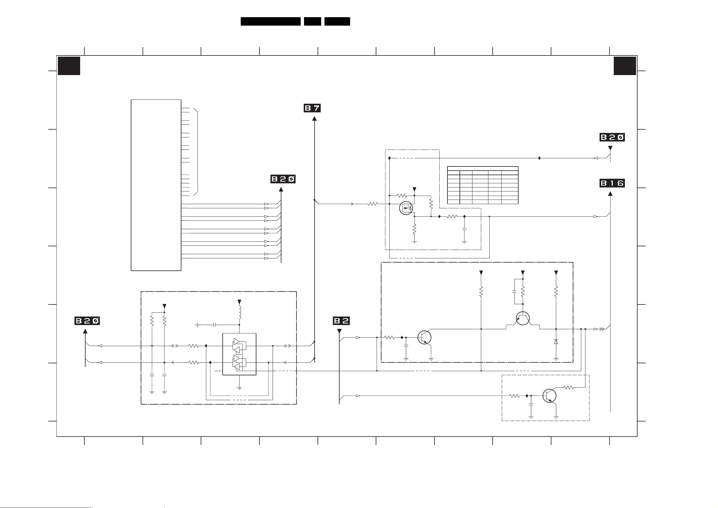
SSB: Scaler Interface
Circuit Diagrams and PWB Layouts
60LC4.31E AA 7.
1234
B9 B9
A
B
C
SCALER INTERFACE
7801-8
GM1501-LF-CF
ACp|GPIO_G06_B6|DORED8
ACn|GPIO_G06_B7|DORED9
A3p|GPIO_G06_B4|DORED6
A3n|GPIO_G06_B5|DORED7
A2p|GPIO_G05_B1|DOGRN3
A2n|GPIO_G05_B2|DOGRN4
A1p|GPIO_G05_B4|DOGRN6
A1n|GPIO_G05_B5|DOGRN7
A0p|GPIO_G05_B6|DOGRN8
A0n|GPIO_G05_B7|DOGRN9
SHIELD5|DEBLU5
SHIELD4|DEBLU2
SHIELD3|DEGRN5
SHIELD2|DEGRN4
SHIELD1|DEGRN3
SHIELD0|DEGRN2
BCp|DEGRN8
BCn|DEGRN9
B3p|DEGRN6
B3n|DEGRN7
B2p|DEBLU3
B2n|DEBLU4
B1p|DEBLU6
B1n|DEBLU7
B0p|DEBLU8
B0n|DEBLU9
LVDS
AE20
AF20
AE19
AF19
AE21
AF21
AE22
AF22
AE23
AF23
AD14
AE13
AE11
AD11
AC11
AF10
AE12
AF13
AF11
AF12
AF14
AE14
AF15
AE15
AF16
AE16
TO SCALER
NC
TO PACIFIC3
TXBC+
TXBC-
TXB3+
TXB3-
TXB2+
TXB2-
TXB1+
TXB1-
TXB0+
TXB0-
BU_LHT_ADJ1
56789
RESERVED
IA07 IA05
4A02
RES
BACKLIGHT CONTROL
5V DC 5V PWM 3V3 DC 3V3 PWM
3A03
390R
390R
RES
+5VSWI
RES
3A03
3A02
1K0
SI2301DS-T1
2
1
3
7A01
3A04
1K0
4A03
*
FOR LARGE SCREEN 37"~50"
3A05
RES
IA06
3A05
3A04
7A01
4A03
3A06
2A03
3A06
10K
1K
Y
-
10K
1u
IA00
2A03
1u0
+3V3STBY +3V3STBY
-
-
-
1K
-
Y
-
-
Y
0R
10K
-
1u
-
-
-
-
Y
0R
-
BACKLIGHT_DIM
TO TOP CONNECTORS
BACKLIGHT_CTRL
+5V
D
FROM PACIFIC3
A
B
C
D
2A00 E3
2A01 F2
2A02 F2
2A03 C7
2A12 E6
2A13 D8
2A14 F8
3A00 E2
3A01 E2
3A02 C5
3A03 C6
3A04 C6
3A05 C6
3A06 C7
3A07 E2
3A08 E2
3A10 E6
3A11 D7
3A13 D8
3A14 D9
3A15 F9
3A16 F8
4A00 F3
4A01 F3
4A02 B6
4A03 D6
4A04 F4
4A05 F6
4A06 F8
5A00 E3
6A01 E9
7801-8 A2
7A00 E4
7A01 C6
7A02 E6
7A03 E8
7A04 F8
IA00 C7
IA03 E6
IA05 B8
IA06 C7
IA07 B6
IA08 E3
IA09 E3
IA10 F8
E
F
3139 123 6117.2
TO PACIFIC3
FOR PDP ONLY
+3V3SW
3A08
3A07
10K10K
SDA_DMA_BUS1_DISP SDA_IO
SCL_DMA_BUS1_DISP
2A02
2A01
100p100p
3A00
68R
3A01
68R
2A00 100n
IA08
IA09
1
NC (PDP)
+3V3SW
5A00
8
7A00
PCA9515ADP
VCC
3SDA06 SDA1
4A04
SCL_IO
BUF_ENABLE
SCL0 27 SCL1
RES
RES
5EN
NC
GND
4
4A00
4A01
FROM HERCULES
SC_STANDBY
IA03
3A10
10K
LS|PDP_DVB_SEMISTANDBY
BC847BW
2A12
10n
7A02
4A05
3A11
4K7
2A13
100n
7A03
BC847BW
4A06
3A13
10K
FOR PDP DVB ONLY
BC847BW
IA10
3A16
10K
2A14
10n
7A04
6A01
3A14
4K7
BZX384-C3V9
3A15
3K3
STANDBY
RESERVED
G_16210_009.eps
123456789
E
F
160106
Page 61

Circuit Diagrams and PWB Layouts
61LC4.31E AA 7.
SSB: SDRAM
123456789
B10 B10
A
B
C
D
E
F
SDRAM
+2V5_DDR
47u
16V
2B022B01
47u
6.3V
2B03
TO/FROM SCALER
100n100n
2B052B04
FSRAS
FSCAS
FSWE
FSCLK+
FSCLKFSCKE
FSDQM(0)
FSDQM(1)
FSDQM(2)
FSDQM(3)
FSBKSEL(0)
FSBKSEL(1)
FSADDR(0)
FSADDR(1)
FSADDR(2)
FSADDR(3)
FSADDR(4)
FSADDR(5)
FSADDR(6)
FSADDR(7)
FSADDR(8)
FSADDR(9)
FSADDR(10)
FSADDR(11)
100n100n
FSVREF
2B072B06
IB03
IB02
100n100n
+2V5_DDR
3B01
FB01
3B02
2B092B08
10K
1%
10K
1%
K4D263238F-UC50
150R3B03 1%
100n100n
+2V5_DDR
2B152B14
100n
86
NC
0
1
2
3
4
5
6
D
7
8
9
10
11
12
13
14
15
16
17
18
19
20
21
22
D
23
24
25
26
27
28
29
30
31
DQS
2B112B10
100n100n
2B19
RES
2B18
22u16V
2B17
100n
7B01
5816
65962958142259677379
15
35
VREF
28
CS
RAS
26
CAS
25
WE
55
CK
54
CK
53
CKE
23
0
56
1
DM
24
2
57
3
29
0
30
BA
1
31
0
32
1
33
2
34
3
47
4
48
5
A
49
6
50
7
51
8
45
9
36
10
37
11
38
39
40 77
NC
41
42
43
93
RFU
52
MCL
VSS VSSQ
466685
2B132B12
100n100n
Φ
SDRAM
1M X 32 X 4
5
111962
VDDQVDD
7076829299
100
2B16
100n
TO/FROM SCALER
FSDATA(0)
FSDATA(1)
FSDATA(2)
FSDATA(3)
FSDATA(4)
44
87
8827
89
90
91
97
98
1
3
4
6
7
60
61
63
64
68
69
71
72
9
10
12
13
17
18
20
21
74
75
78
80
81
83
84
94
FSDATA(5)
FSDATA(6)
FSDATA(7)
FSDATA(8)
FSDATA(9)
FSDATA(10)
FSDATA(11)
FSDATA(12)
FSDATA(13)
FSDATA(14)
FSDATA(15)
FSDATA(16)
FSDATA(17)
FSDATA(18)
FSDATA(19)
FSDATA(20)
FSDATA(21)
FSDATA(22)
FSDATA(23)
FSDATA(24)
FSDATA(25)
FSDATA(26)
FSDATA(27)
A
B
C
D
E
F
2B01 A1
2B02 A1
2B03 A2
2B04 A2
2B05 A2
2B06 A3
2B07 A3
2B08 A3
2B09 A3
2B10 A4
2B11 A4
2B12 A4
2B13 A5
2B14 A5
2B15 A5
2B16 A5
2B17 B4
2B18 B4
2B19 B4
3B01 B3
3B02 B3
3B03 C3
7B01 C4
FB01 B3
IB02 C3
IB03 C3
G
3139 123 6117.2
FSDATA(28)
FSDATA(29)
FSDATA(30)
FSDATA(31)
FSDQS
G_16210_010.eps
G
160106
123456789
Page 62

Circuit Diagrams and PWB Layouts
62LC4.31E AA 7.
SSB: Flash / Control
1234567
B11 B11
FLASH / CONTROL
+3V3_IO
+3V3_IO
A
B
C
D
E
F
TO SCALER
OCMADDR(1)
OCMADDR(2)
OCMADDR(3)
OCMADDR(4)
OCMADDR(5)
OCMADDR(6)
OCMADDR(7)
OCMADDR(8)
OCMADDR(9)
OCMADDR(10)
OCMADDR(11)
OCMADDR(12)
OCMADDR(13)
OCMADDR(14)
OCMADDR(15)
OCMADDR(16)
OCMADDR(17)
OCMADDR(18)
+3V3_IO
#OCM_WE
#OCM_RE
#ROM_CS
NVM_WP_SCALER
SCL_IO
SDA_IO
3C22
3C23 220K
1K0
FC11
2C04
10n 10n
M29W400DT-55N6
25
24
23
22
21
20
19
18
8
7
6
5
4
3
2
1
48
17
15
12
11
28
26
47
2C05
+3V3SW
0V
3V2
3V2
7C03
EPROM
512Kx8/256Kx16
0
1
2
3
4
5
6
7
8
9
10
11
12
13
14
15
16
17
RB
RP
WE
OE
CE
BYTE
3C00
10K
FC01
FC02
FC03
0
A
4M-1
27
2C02
100n
7
WC
6
SCL
5
5C00
FC00
37
D
46
+3V3SW
3V2
8
Φ
(4Kx8)
EEPROM
4
2C00
100n
2C01
16V10u
29
0
31
1
33
2
35
3
38
4
40
5
42
6
44
7
30
8
32
9
34
10
36
11
39
12
41
13
43
14
45
15
A-1
10
ADR
0
1
2SDA
13
14
16
7C01
NC
M24C32-WMN6
TO SCALER
OCMDATA(0:7)
OCMDATA(0)
OCMDATA(1)
OCMDATA(2)
OCMDATA(3)
OCMDATA(4)
OCMDATA(5)
OCMDATA(6)
OCMDATA(7)
OCMADDR(0)
9
1
2
3
2
4
OCMADDR(0:19)
1C00
SKQR
For Software
Development
only - (RES)
OCMADDR(0)
OCMADDR(1)
OCMADDR(2)
OCMADDR(3)
OCMADDR(4)
OCMADDR(5)
OCMADDR(6)
OCMADDR(7)
OCMADDR(8)
OCMADDR(9)
OCMADDR(10)
OCMADDR(11)
OCMADDR(12)
OCMADDR(15)
OCMADDR(17)
OCMADDR(18)
OCMADDR(16)
OCMADDR(14)
OCMADDR(13)
OCMADDR(19)
FC04
1
3
2C03
100n
3C01
0R
3C06-1 10K1
3C06-2 10K
3C06-3 10K
3C06-4 10K
3C08-1 10K18
3C08-2 10K27
3C08-3 10K3
3C08-4 10K
3C10-1 10K
3C10-3 10K36
3C10-4 10K4
3C10-2 10K27
+3V3SW
3V2
5
1
MR
VCC
SUB
2
8
27
36
45
18
45
27
36
45
18
7C02
PST596J
VOUT
GND
3
10K3C07-1
10K3C07-2 2 7
10K3C07-3 3 6
10K3C07-4 4 5
6
10K3C09-1 1 8
10K3C09-2
10K3C09-3
10K3C09-4
5
FC05
4
3V20V
10K
10K
10K
10K
36
183C04-1
3C04-4 4 5
3C04-2 2 7
3C04-3
3C02
1K0
#RESET
3C03
RES
3C05 10K
+3V3_IO
3C17
3C16-4
45
FC06
TO SCALER
10K
10K
3C16-1
3C16-3
36
18
FC09
FC08
FC07
3C19
RES RES RES
3C213C20
&
TO COLUMBUS
3C18
10K
3C16-2
27
FC10
A
B
C
D
E
F
1C00 E4
2C00 A3
2C01 B3
2C02 E2
2C03 E4
2C04 D1
2C05 D1
3C00 E2
3C01 F4
3C02 E6
3C03 F6
3C04-1 B6
3C04-2 B6
3C04-3 B6
3C04-4 B6
3C05 B6
3C06-1 B5
3C06-2 B5
3C06-3 B5
3C06-4 B5
3C07-1 C5
3C07-2 C5
3C07-3 C5
3C07-4 C5
3C08-1 C5
3C08-2 C5
3C08-3 C5
3C08-4 C5
3C09-1 C5
3C09-2 C5
3C09-3 C5
3C09-4 C5
3C10-1 D5
3C10-2 D5
3C10-3 D5
3C10-4 D5
3C16-1 C7
3C16-2 C7
3C16-3 C6
3C16-4 C6
3C17 C6
3C18 C7
3C19 D6
3C20 D7
3C21 D7
3C22 D1
3C23 D1
5C00 A2
7C01 E3
7C02 E5
7C03 B2
FC00 A2
FC01 E2
FC02 F2
FC03 F2
FC04 F4
FC05 F5
FC06 D6
FC07 D6
FC08 C7
FC09 C7
FC10 C7
FC11 D1
3139 123 6117.2
G_16210_011.eps
160106
1234567
Page 63

SSB: HDMI
2D00 A10
2D01 B10
2D02 F2
2D08 B1
2D09 B1
2D10 B2
2D11 B2
2D12 B1
2D13 B1
2D14 B2
123456789101112131415
2D15 B2
2D16 B2
2D17 B2
2D18 B2
2D21 E2
2D22 E2
2D23 E2
2D24 E2
2D25 E2
2D29 C1
Circuit Diagrams and PWB Layouts
2D30 D1
2D31 D1
2D32 E1
2D34 E2
2D35 E2
2D36 E2
2D37 E2
2D38 E2
2D39 E2
2D42 G2
2D43 G2
2D44 G2
2D45 H1
2D46 H2
2D47 I2
2D48 I3
2D49 H5
2D50 G9
2D51 G9
2D52 G10
2D53 G10
2D54 G11
2D55 G11
2D56 H10
2D57 H10
2D58 I11
2D59 I11
3D00 A9
3D01 A10
3D02 B9
3D03 B10
3D05 I4
3D06 I4
3D07 E10
3D08 E10
3D09 A10
3D10 B10
3D11 E13
3D15-1 C14
3D15-2 C14
3D15-3 C14
3D15-4 C14
3D16-1 D14
3D16-2 D14
3D16-3 D14
63LC4.31E AA 7.
3D16-4 C14
3D17-1 B14
3D17-2 B14
3D17-3 B14
3D17-4 A14
3D18 F10
3D19 F9
3D20-1 G8
3D20-2 H8
3D20-3 H8
3D20-4 G8
3D21-1 B14
3D21-2 B14
3D21-3 B14
3D21-4 B14
3D22 E14
3D23 D14
3D24 H11
3D26 H11
3D27 H4
4D02 G8
4D03 H8
4D04 I4
4D05 I4
4D06 I4
5D00 F1
5D01 G1
5D02 G1
5D03 H2
5D04 I2
5D05 H2
5D06 F1
7D00 A8
7D01 B8
7D02 H1
7D03-1 A11
7D03-2 G6
7D03-3 A5
7D04 G9
7D05 H4
FD01 B9
FD02 B9
FD03 C9
FD04 C9
FD05 E15
FD06 E15
FD07 G1
FD08 G1
FD09 G1
FD10 I2
FD11 I2
FD12 F1
FD13 G9
FD14 H2
FD15 G9
FD17 A9
ID00 H1
ID01 H2
ID08 H10
ID09 H11
ID10 G10
ID11 H11
ID13 E15
ID14 D15
ID18 H14
ID19 I14
ID20 A9
ID22 E10
ID24 I5
ID25 I4
ID28 G8
B12
A
B
C
D
E
VDDA_3V3PLL
VDDA_1V8
VDDA_3V3
VDDD_1V8
VDDC_1V8
VDDI_3V3
VDDD_3V3
HDMI
1n0
1n0
1n0
2D09
2D08
2D10
1n0
1n0
1n0
2D13
2D12
2D14
2D29 1n0
1n0
1n0
2D30
2D31
1n0
1n0
2D34
2D32
2D21 1n0
1n0
2D11
1n0
2D15
1n0
2D35
100n
2D22
1n0
2D16
1n0
2D36
1n0
2D23
1n0
2D37
1n0
2D24 1n02D17
1n0
2D18
1n0
2D38
2D25 100n
1n0
2D39
M11
N11
M10
N10
P10
P11
N12
N13
N14
E12
E13
D10
D11
D12
D13
D14
G13
F13
N7
M7
M9
N9
D8
D9
E6
T4
D4
E4
F4
G4
H4
J4
K4
L4
M4
VDDAPLL
VDD18APLL
VDDR
VDDG
VDDB
VDDBIAS
VDDSOG
VDDFRO
VDDPLL
VDD18PLL
VDD18HDMI
VDD18RRX
VDDRX2A
VDDRX2B
VDDRX1A
VDDRX1B
VDDRX0A
VDDRX0B
VDDRXC
1
VDD18CORE
2
OTP7V
VDDIN
VDDQ0
VDDQ1
VDDQ3
VDDQ4
VDDQ5
VDDQ6
VDDQ7
VDDQ8
VDDQ9
F6
H6
G6
FROM DIGITAL-IO
7D03-3
TDA9975
SUPPLY
THERMAL GROUNDS
J6
J7
L6
L7
F8
F7
K6
K7
H8
H7
G8
G7
J9
J8
L8
L9
F9
K8
K9
H9
G9
J10
L10
F10
K10
H10
G10
GNDAPLL
GNDHDMI
GNDCORE
F11
G11
GNDAVI
GNDI2C
GNDOUT
J11
H11
M5
N5
P5
R5
T5
M8
N8
P6
P7
P8
P9
R10
R11
M12
P12
P13
P14
P15
R15
T15
M6
N6
A8
B8
C8
B9
B10
B11
B12
B13
B14
B15
B16
E7
E8
E9
E10
E11
F12
C7
D6
D7
E5
F5
D5
G5
J5
K5
L5
H5
L11
K11
/
+5VHDMI_A
DOC_SCLA
DOC_SDAA
+5VHDMI_B
DOC_SCLB
DOC_SDAB
RX2+A
RX2-A
RX1+A
RX1-A
RX0+A
RX0-A
RXC+A
RXC-A
RX2+B
RX2-B
RX1+B
RX1-B
RX0+B
RX0-B
RXC+B
RXC-B
FD17
7D00
M24C02-WMN6
1
2
3
M24C02-WMN6
1
2
3
84
Φ
(256x8)
EEPROM
0
1
ADR
2SDA
7D01
84
Φ
(256x8)
EEPROM
0
1
ADR
2SDA
7D03-1
TDA9975
3D01
3D00
47K
4K7
7
ID20
WC
6
SCL
5
FD01
FD02
3D02
3D03
4K7
47K
7
ID15
WC
6
SCL
5
FD03
FD04
3D08 1K0
3D09
47K
47K
2D00
100n
2D013D10
100n
1%
1K03D07
1%
ID22
T10
RBIAS
NC
T16
1
R16
HCSYNC
P16
3
N16
1
M16
VSYNC
NC
N15
3
T12
1
R12
SOG
T11
3
T14
1
R14
R/Pr
T13
3
T9
1
R9
G/Y
NC
T8
3
T7
1
R7
B/Pb
T6
3
R13
Rref
R8
Gref
R6
Bref
A9
RX2+A
A10
RX2-A
A12
RX1+A
A13
RX1-A
A15
RX0+A
A16
RX0-A
F16
RXC+A
G16
RXC-A
K15
HSCL A
K16
HSDA A
C10
RX2+B
C9
RX2-B
C13
RX1+B
C12
RX1-B
C16
RX0+B
C15
RX0-B
G14
RXC+B
F14
RXC-B
J15
HSCL B
J16
HSDA B
D15
RRXB
D16
RRXA
Φ
IN/OUT
VPA0
VPA1
VPA2
VPA3
VPA4
VPA5
VPA6
VPA7
VPA8
VPA9
VPA10
VPA11
VPB0
VPB1
VPB2
VPB3
VPB4
VPB5
VPB6
VPB7
VPB8
VPB9
VPB10
VPB11
VPC0
VPC1
VPC2
VPC3
VPC4
VPC5
VPC6
VPC7
VPC8
VPC9
VPC10
VPC11
VCLK
HREF
VREF
FREF
CS
HS
VS
/VAI
DE
PL
E1
E2
F1
F2
G1
G2
H1
H2
J1
J2
K1
K2
L1
L2
M1
M2
N1
N2
P1
P2
R1
R2
NC NCNC
T1
T2
E3
F3
G3
H3
J3
K3
L3
M3
N3
P3
R3
T3
D1
D2
C1
C2
B2
A2
A1
B1
A3
A4
3D17-3
3D17-2
3D17-1
3D21-4
3D21-3
3D21-2 33R
3D21-1 33R1
3D15-4 4 5
3D15-3 3 6
3D15-2
3D16-4 4 5
3D16-2 33R27
3D16-1 1 8
3D23 33R
3D22
3D11
5K6
27
18
HDMI_CbCr(0)
33R3D17-4 4 5
HDMI_CbCr(1)
33R36
HDMI_CbCr(2)
33R27
HDMI_CbCr(3)
33R18
HDMI_CbCr(4)
33R45
HDMI_CbCr(5)
33R36
HDMI_CbCr(6)
HDMI_CbCr(7)
8
HDMI_Y(0)
33R
HDMI_Y(1)
33R
HDMI_Y(2)
33R27
HDMI_Y(3)
33R3D15-1
HDMI_Y(4)
33R
6
HDMI_Y(5)
33R3D16-3 3
HDMI_Y(6)
HDMI_Y(7)
33R
ID14
FD05
FD06
ID13
33R
HDMI_CbCr(0:7)
HDMI_Y(0:7)
HDMI_VCLK
TO SCALER
H_HDMI
V_HDMI
HDMI_INT
HDMI_VDV
HDMI_PL
TO SCALER
A
B
C
D
E
+3V3SW
F
G
LD1086D2T18
ID00
3
2D45
H
100n
I
3139 123 6117.2
123456789101112131415
5D06
5D00
5D01
5D02
7D02
COM
FD12
2D02
22u
6.3V
FD07
FD08
FD09
2D42
2D43
22u
22u
6.3V
6.3V
5D05
FD14
ID01
2
OUTIN
1
120R
2D46
47u
6.3V
5D03
FD10
FD11
5D04
120R
2D47
22u
6.3V
2D44
22u
6.3V
2D48
22u
6.3V
VDDA_3V3PLL
VDDA_3V3
VDDD_3V3
VDDI_3V3
VDDC_1V8
VDDA_1V8
VDDD_1V8
VDDI_3V3
HDMI_PD
ADC_XOUT
SCL_IO
SDA_IO
3D27
3K3
7D05
2560TK
1
13M5
4
3
2
ID25
3D05 100R
VDDA_3V3
1n0
2D49
4D04
4D05
4D06
100R3D06
7D03-2
TDA9975
C11
TM0
C14
TM1
A14
TM2
A11 K14
TM3
H12
AUX0
H13
AUX1
G12
AUX2
G15
AUX3
F15
AUX4
E14
AUX5
E15
AUX6
E16
AUX7
L12
CCLK
M13
CKEXT
M14
COAST
H15
GCP
H14
CLAMP
H16
ID24
PD
M15
MCLK
J13
/OE
L15
SCL
L16
SDA
CTRL
TDO
TRST
TCK
OR G/Y
OR B/U
OR R/V
CTL0
CTL1
CTL2
CTL3
AP0
AP1
AP2
AP3
ACLK
WS
TMS
DIS
+3V3SW
+3V3SW
3D19
1R0
2D50
FD13
47u
6.3V
UDA1334ATS
FD15
2D51
100n
7D04
13
BCK
SYSCLK
PLL1
DATAI
PLL0
0
SFOR
1
WS
MUTE
VDDA
DAC
15
Φ
VREF_DAC
VSSA
CLKOUT
VSSD
5
VOUTL
VOUTR
1
6
3
10
11
7
2
8
K13
TDI
L13
L14
J14
D3
C3
B3
R4
X0
P4
X1
X2
A0
NC
N4
C6
C5
C4
B4
A7
A6
NC
B6
NC
B5
NC
A5
B7
K12
J12
+3V3SW
ID28
4D024D03
3D20-1
3D20-4
3D20-3
3D20-2
33R18
45
33R
36
33R
7
33R2
4
DEEM
3D18
1R0
47u
VDDD
2D52
2D53
100n
6.3V
12
14
16
ID08
9
AUDIO DAC
ID10
2D56
2D54 2D55
47u 6.3V
ID09
10u
16V
10u2D57
ID11
16V
3D26
220R
2D59
10n
100n
3D24
220R
2D58
10n
ID18
ID19
TO HERCULES
HDMI_AudioINR
HDMI_AudioINL
G_16210_012.eps
F
G
H
I
160106
Page 64

Circuit Diagrams and PWB Layouts
64LC4.31E AA 7.
SSB: MUX-Sync Interface
123456789101112
B13 B13
A
B
C
D
E
F
G
H
3139 123 6117.2
MUX-SYNC INTERFACE
/
FROM HERCULES / SYNC INTERFACE
R_OTC_SDTV
G_OTC_SDTV
B_OTC_SDTV
(SCART) (CINCH)
FROM ANALOG-IO
(SCART) (CINCH)
SYNC INTERFACE
FROM SCART-IO/ CINCH-IO
(SCART) (CINCH)
/
SC1_CVI_DMMI_R_Pr_IN
SC1_CVI_DMMI_G_Y_IN
SC1_CVI_DMMI_B_Pb_IN
RINA|Pr
GINA|YINA
BINA|Pb
/
Hsync_SDTV
FBL_HSYNC_PIN16_IN
Vsync_SDTV
VSYNC_IN
/
FE00
FE01
FE02
2E33
4u7
2E34
4u7
2E35 4u7
3E31 100R
100R3E32
100R3E33
100R3E34
IE50
2E00
2E01
2E02
IE09
6E00
BZX384-C2V7
IE11
6E02
BZX384-C2V7
4u7
IE13
4u7
IE14
4u7
IE15
IE18
FOR CINCH ONLY
RES
4E10
IE10
6E01
BZX384-C2V7
IE12
6E03
BZX384-C2V7
3E50 47K
IE16
47K3E53
+5VSWI
47K3E51
47K3E52
IE45
47K3E55
3E54 47K
7E03
74HC4053D
6
13
12
11
1
2
10
3
5
9
3V2
SD_HD_SEL
47K
3E06
47K
3E11
+3V3SW
VDD
MDX
G4
1
2
4X1
4X2
VEE VSS
7
4E11
47K
3E07
47K3E10
16
RES
5E03
8
3E08 47K
47K3E09
2E31
FOR CINCH ONLY
+5VSWI
3E00 56R
3E01 56R
3E02 56R
4u7
2E21
4u7
2E22
4u7
2E23
3E40
RES
3E41
RES
3E42
RES
150R
3E60 150R
3E59
3E58 150R
+3V3SW
7E05-1
74LVC14APW
1
7E05-3
74LVC14APW
5
14
10
7
IE43
IE44
COL_Do(8)COL_Di(9)_INV
IE01
IE02
IE20
IE22
IE23
IE04
9
23
22
26
25
27
2
1
3
6
5
7
20
21
+5VSWI
5E01
181512
VCC
DISABLE
THROUGH
MUXSEL
GSR1
RINA|YINA
RINB|YINB
GSG1
GINA|UINA
GINB|UINB
GSB1
BINA|VINA
BINB|VINB
RFC
VFC
GND
161310
FROM ADC
COL_Di(9)
FE06
Φ
24
VCC
ROUT|YOUT
GOUT|UOUT
BOUT|VOUT
GND_HS
19
29
30
3E37
22R
2E16
2E17
2E18
2E19
7E01
SM5301BS-G
NC1
NC2
NC3
FE07
74LVC14APW
4
8
28
17
14
11
B-PB-ADC
7E05-5
100n
100n
100n
100n
47u2E20
6.3V
R-PR-ADC
G-Y-ADC
4u7
3E19
56R
3E20
56R
3E21
56R
3E22
100K
12
2E04
2E05
IE48
2E06
IE49
3E183E173E16
0V
RES
3V2
IE25
2E07
33p
IE26
2E09
33p
IE39
2E11
33p
2E13
1u0
3E39
4
100R
IE40
3E38
8
100R
3E463E43
100R
2E08
4u7
2E10
4u7
2E12
4u7
2E14
IE27
AHSYNC
IE24
AVSYNC
II_PC_HD_SEL
IE35
4u7
IE36
4u7
IE37
FE04
FE05
3E23
820R33p
3E13
3E14
3E15
RGB TEXT FOR
HER OTC
*
3E13
330R JMP
3E14
330R JMP
3E15
330R JMP
3E16
+5VSWI
100n
14
15
4
5E00
7E00
ADG733BRU
12
13
2
1
5
3
S1A
S1B
S2A
S2B
S3A
S3B
VSS
IE00
16
VDD
Φ
EN
A0
A1
A2
D1
D2
D3
GND
7
8
IE42
PC_HD_SEL
2E03
100n
11
10
14
15
3E35
100R
3E36
100R
100R
3E12
6
9
4
330R RES
3E17
330R RES
3E18
330R RES
10K
RGB|CVI_HDA_SEL
FE03
SC1_R_CVI_Pr_IN
SC1_G_CVI_Y_IN
SC1_B_CVI_Pb_IN
7E04-1
74LVC14APW
1
7E04-3
74LVC14APW
5
7E04-5
74LVC14APW
11
+3V3SW
14
7
14
FROM SCALER
3V2
IE19
IE38
IE21
TO SCALER
14
7
7
SD_HD_SEL
HD_FILTER
0V
I_PC_HD_SEL
2
6
10
3
9
13
*
*
*
IE03
3E57
10R
7E04-2
74LVC14APW
14
7
7E04-4
74LVC14APW
14
7
14
7
IE47
***
4E03
2E32
100n
7E04-6
74LVC14APW
IE05
IE06
IE07
FE10
FE11
FE12
FE13
14
7
14
7
IE17
IE29
IE30
3E49
22R
5E02
16
18
20
2
0V6
1
2V7
14
0V8
15
12
0V4
11
2V7
4
5
3E24
3E25
3E26
3E27
3E28
3E29
3E30
74LVC14APW
2
74LVC14APW
6
74LVC14APW
123456789101112
S1
D1
S2
D2
S3
D3
S4
D4
GND_HS
7E05-2
3
7E05-4
9
7E05-6
13
IE08
5V4
13
VDD
SPST
SWITCH
NC
470R
39R
22R
39R
22R
39R
22R
2E15
100n
Φ
21
IE32
IE34
14
7
14
7
14
7
NC
IN1
IN2
IN3
IN4
GND
3
100n2E24
2E25 100n
100n2E26
100n2E27
2E28 100n
2E29 100n
100n
2E30
2E36
100n
4
8
1211
7E02
ADG781BCP
6
8
10
19
3V2
FE08
17
3V3
9
7
IE33
IE46
IE28
TO SCALER
SOG
R_PR+
R_PR-
G_Y+
G_Y-
B_PB+
B_PB-
COL_Do(8)_INV
TO SCALER
G_16210_013.eps
160106
A
B
C
D
E
F
G
H
2E00 C3
2E01 C3
2E02 C3
2E03 B5
2E04 B7
2E05 B7
2E06 B7
2E07 C7
2E08 C8
2E09 D7
2E10 C8
2E11 D7
2E12 D8
2E13 D7
2E14 D8
2E15 A11
2E16 B9
2E17 B9
2E18 B9
2E19 B9
2E20 B9
2E21 B10
2E22 B10
2E23 B10
2E24 C11
2E25 C11
2E26 C11
2E27 C11
2E28 D11
2E29 D11
2E30 D11
2E31 E4
2E32 E7
2E33 C2
2E34 C2
2E35 D2
2E36 E11
3E00 A10
3E01 A10
3E02 A10
3E06 C4
3E07 C4
3E08 C4
3E09 D4
3E10 D4
3E11 D4
3E12 C5
3E13 B6
3E14 B6
3E15 B6
3E16 B7
3E17 B7
3E18 B7
3E19 C7
3E20 C7
3E21 D7
3E22 D7
3E23 D8
3E24 C10
3E25 C10
3E26 C10
3E27 C10
3E28 D10
3E29 D10
3E30 D10
3E31 F2
3E32 F2
3E33 F2
3E34 F2
3E35 F5
3E36 F5
3E37 G9
3E38 F7
3E39 F7
3E40 C10
3E41 D10
3E42 D10
3E43 G5
3E46 G7
3E49 G10
3E50 C3
3E51 C3
3E52 C4
3E53 D3
3E54 D3
3E55 D4
3E57 D7
3E58 D9
3E59 D9
3E60 D9
4E03 B7
4E10 E3
4E11 G4
5E00 B5
5E01 B8
5E02 A10
5E03 E4
6E00 F3
6E01 F3
6E02 G3
6E03 G3
7E00 C5
7E01 B9
7E02 A11
7E03 E4
7E04-1 E6
7E04-2 E7
7E04-3 F6
7E04-4 F7
7E04-5 G6
7E04-6 G7
7E05-1 E10
7E05-2 E11
7E05-3 F10
7E05-4 F11
7E05-5 G9
7E05-6 G11
FE00 B2
FE01 B2
FE02 B2
FE03 C6
FE04 C8
FE05 D8
FE06 B9
FE07 E9
FE08 B11
FE10 C10
FE11 C10
FE12 C10
FE13 D10
IE00 B5
IE01 B8
IE02 B8
IE03 D7
IE04 D8
IE05 B10
IE06 B10
IE07 B10
IE08 A11
IE09 F3
IE10 F3
IE11 F3
IE12 F3
IE13 C3
IE14 C3
IE15 C3
IE16 C3
IE17 A10
IE18 D3
IE19 C6
IE20 C8
IE21 D6
IE22 C8
IE23 D8
IE24 F7
IE25 C7
IE26 C7
IE27 F7
IE28 G11
IE29 A10
IE30 A10
IE32 C11
IE33 C11
IE34 C11
IE35 B8
IE36 B8
IE37 B8
IE38 C6
IE39 D7
IE40 F7
IE42 F5
IE43 G10
IE44 G10
IE45 C4
IE46 C11
IE47 B7
IE48 B7
IE49 B7
IE50 C3
Page 65

SSB: Digital I/O
1F01 A5
1F02 A1
1F03 C1
2F01 C9
2F02 C9
2F03 C9
2F04 D9
2F13 A7
2F14 A7
12345678910
2F15 A8
2F16 A8
3F01 B2
Circuit Diagrams and PWB Layouts
3F02 B2
3F03 D2
3F04 D2
3F05 C6
3F06 C6
3F07 C7
3F08 C7
3F09 C7
3F10 C7
3F11 C8
3F12 C8
3F13 D6
3F14 D6
3F15 D7
3F16 D7
3F17 D7
3F18 D7
3F19 D8
3F20 D8
3F24 A7
3F25 A7
3F26 A7
3F27 A7
7F01 B2
7F02 D2
7F03 C8
FF01 A1
65LC4.31E AA 7.
FF02 A1
FF03 A1
FF04 A1
FF05 A1
FF06 A1
FF07 A1
FF08 A1
FF09 B1
FF10 B1
FF11 B1
FF12 B1
FF13 B1
FF14 C1
FF15 C1
FF16 C1
FF17 C1
FF18 C1
FF19 C1
FF20 C1
FF21 D1
FF22 D1
FF23 D1
FF24 D1
FF25 D1
FF26 D1
IF01 A6
IF02 A6
IF03 A7
IF04 A7
IF05 C6
IF06 C6
IF08 C6
IF09 D6
IF10 D6
IF12 D6
IF13 C9
IF14 D9
IF16 B3
IF17 B2
IF18 D2
S001 A6
S002 B6
B14 B14
A
B
C
D
DIGITAL IO
1F02
DC1R019JDA
1
2
3
4
5
6
7
8
9
10
11
12
13
14
15
HDMI CONNECTOR-1
16
17
18
19
2021
2223
1F03
DC1R019JDA
1
2
3
4
5
6
7
8
9
10
11
12
13
14
15
HDMI CONNECTOR-2
16
17
18
19
2021
22
23
CEC
CEC
FF02
FF15
FF01
FF03
FF04
FF05
FF06
FF07
FF08
FF09
FF10
FF11
FF12
FF13
FF14
FF16
FF17
FF18
FF19
FF20
FF21
FF22
FF23
FF24
FF25
FF26
BC847BW
BC847BW
7F01
7F02
3F01 1K0
IF17
IF18
3F04 2K2
TO HDMI
RX2+A
RX2-A
RX1+A
RX1-A
RX0+A
RX0-A
RXC+A
RXC-A
DOC_SCLA
DOC_SDAA
+5VHDMI_A
IF16
2K23F02
1K03F03
HDMI_HOTPLUG_RESET
RX2+B
RX2-B
RX1+B
RX1-B
RX0+B
RX0-B
RXC+B
RXC-B
DOC_SCLB
DOC_SDAB
+5VHDMI_B
TO SCALER
MSD-242V-01 NIDIP
FROM SIDE-IO
1F01
Analog_AudioSEL2
Analog_AudioSEL1
AV1_AudioINR
DMMI_AudioINR
AV2_AudioINR
SIDE_AudioINR
AV1_AudioINL
DMMI_AudioINL
AV2_AudioINL
SIDE_AudioINL
FROM/TO SCART-IO
+5VSW
3F09
33K
33K33K
IF04
2F14
180p
IF03
180p
3F10
3F18
33K
3F27
15K
2F16 2u2
3F262F13
15K
33K33K
3F193F17
33K 33K
3F123F11
33K
3F20
2u22F15
74HC4052D
10
9
6
12
14
15
11
1
5
2
4
+5VSW
7F03
4X
1
G4
0
1
2
3
0
1
2
3
VEE VSS
16
VDD
030
MDX
7
DVI_D_AudioINL
DVI_D_AudioINR
2F01
IF13
13
IF14
3
8
2F02
100n
16V10u
2F03
4u7
2F04
4u7
Analog_AudioINR
Analog_AudioINL
1
3
2
B15A
B15B
B15A
B15A
B15B
B15A
IF02
IF01
S002
S001
+5VSW
3F05
33K
IF05
IF06
IF08
IF09
IF10
IF12
3F24 10K
3F25 10K
3F06
33K33K
3F143F13
3F07
33K33K
3F08
33K33K
3F163F15
AUDIO-IN (DVI-D)
To HERCULES
/
A
B
C
D
3139 123 6117.2
12345678910
G_16210_014.eps
160106
Page 66

Circuit Diagrams and PWB Layouts
66LC4.31E AA 7.
SSB: SCART Analog I/O
12345678910111213141516
B15A B15A
A
B
C
D
E
F
G
H
I
J
K
SCART ANALOG-IO
FG00
SCART 1
CON_SCART
1G01-1
MRC-PJ08-01 NI
1G01-2
26
27
24
25
22
23
RED-BLUE-GREEN
MRC-PJ08-01 NI
MT
1G01-3
29
28
MRC-PJ08-01 NI
CON_SCART
1G02-1
MRC-PJ08A-02 NI
MT
1G02-3
28 29
MRC-PJ08A-02 NI
1
2
FG01
3
FG03
FG02
4
5
6
FG04
7
8
9
10
11
12
13
14
15
16
17
18
19
20
21
1
2
FG17
3
FG18
4
5
6
FG21
7
FG22
8
9
10
FG24
11
12
13
14
FG26
15
FG27
16
17
18
FG28
19
20
21
COMPONENT
FG07
S004
FG08
S005
FG10
FG16
S026
S027
AUDIO-IN
FG11
FG12
FG13
FG14
FG19
FG20
FG05
1G02-2
RED-WHITE
MRC-PJ08A-02 NI
S024 S000
S013
S014
S017
S022
S023
Audio-R_out
Audio-R_in
Audio-L_out
Audio-L_in
RGB-B_in
Function_Sw
RGB-G_in
RGB-R_in
RGB-BL_in
Terr_CVBS_out
Video_in
COMPONENT
VIDEO-IN
Audio-R_out
Audio-R_in
Audio-L_out
Audio-L_in
RGB-B_out
Function_Sw
RGB-G_out
RGB-R_out/YC-C_in
FBL_HSYNC_OUT
CVBS_out
Video/YC-Y_in
SCART 2
2G01
RES
2G02
RES
S025
6G01
IG04
6G02
91R
S006
3G09
S010
S009
S029S028
S030
RES
RES
2G19 2G18
S015
6G066G07
S018
6G14
BZX384-C4V3
6G15
BZX384-C4V3
3G30
EMC
2G42
RES
26
27
24
25
3G01 150R
3G38
BZX384-C3V9
BZX384-C3V9
S007
75R
3G12
2G29
RES
2G30
RES
2G44
RES
BZX384-C3V9
BZX384-C3V9
S019
BZX384-C4V3
6G17
68R
6G10
RES
RES
150R
RES
2G07
91R
3G10
3G39 27K
3G13
3G58
S011
3G73
75R
3G74
75R
3G72
75R
3G22 150R
3G23
2G26
6G16
S020
BZX384-C4V3
3G29
1K0
IG48
S031
L
3139 123 6117.2
12345678910111213141516
S003
S008
330R
68R
S012
S016
BZX384-C4V3
6G19
3G28
75R
IG50
S032
6G03
BZX384-C3V9
IG12
6G04
BZX384-C3V9
91R
3G59
IG09
IG10
IG11
EMC
2G15
RES
150R
3G26
3G27 10K
6G08
BZX384-C3V9
6G09
BZX384-C3V9
6G18
S021
BZX384-C4V3
3G34
100R
IG00
2G03
330p
IG01
2G04
330p
3G04
3G05
RES
2G08
3G11
6K8
3G14 1K0
6G05
RES
RES
2G27
6G20
BZX384-C4V3
6G21
BZX384-C4V3
IG24
IG27
IG51
10K3G19
IG49
10K3G18
2G16
3G02
220K
3G03
220K
5V2
1V8
10K
2G28
180p
+5VSW
3G16
75R
2G43
10K
10K
4u7
+5VSW
5G07
7G01
BC847BW
IG20
5G08
2G71
10u
BC847BW
3G20
15K
2G09
180p
2G70 10u
IG22
2V5
IG34
IG36
IG25
2G20
3G24
330p
220K
2G21
3G25
330p 220K
IG21
2G68
180p
5V2
7G02
3V
2G17
180p180p
IG05
2G13
RES
3G31
3G35
2G10
180p
RES
5G04
4G05
5G02
5G03
5G01
IG14
3G21
15K
2G05
*
*
2G11
2G12 2u2
3G06 100R
3G07
3G08
IG23
2G14
IG37
IG33
2G22 10u
2G23 10u
IG15
2G24
4G23
RES
3V7
3G32
RES
RES
2G60
2u2
2G54
2u2
RES
IG35
3G15
3G33
1K0
2u2
16V
2u2
2u22G25
10u2G06
16V
100R
100R
16V
SC1_R
IG02
10u
16V
IG03
AV1_AudioINR
AV1_AudioINL
IG06
IG07
IG08
SC1_FBL_IN
1K0
IG13
FG15
100R3G17
SC2_R_MON_OUT
IG16
IG17
SC2_L_MON_OUT
IG18
IG19
IG26
+5VSW
3G36
47K
3G37
47K
CVI_Pb_IN
CVI_Y_IN
CVI_Pr_IN
4G18
IG52
SC1_R_RF_OUT
SC1_L_RF_OUT
SC1_CVBS_RF_OUT
SC1_CVBS_IN
SC2_CVBS_MON_OUT
IG31
B2
B2
SC1_L
B2
B2
STATUS_1
TO MUX-SYNC INTF
GINA|YINA
BINA|Pb
RINA|Pr
SC2_R
SC2_L
AV2_AudioINR
AV2_AudioINL
STATUS_2_IN|OUT
RGB-B_IN
RGB-G_IN
RGB-R|YC-C_IN
FBL_HSYNC_OUT
SC2_CVBS_MON_OUT1
B15B
B2
HD_AudioINL
B2
HD_AudioINR
B2
SC2_C_IN
FRONT_C_IN
SC2|AV2_SIDE_SW
FRONT_Y_CVBS_IN
3G75
75R
3G76 100R
IG76
4G21
2G66 4u7
4G22
IG73
IG40
2G55 4u7
2G57
4u72G56
4u7
3G96
47K
+5VSW
3G99
47K
3S00
47K
3S03
47K
3G78
47K
3G92
47K
3G77
47K
7G11_12
SC2_Y_IN
DMMI_CVBS_IN|Y_IN
3G93
47K
+5VSW
3G94
47K
3G95
47K
IG42
IG47
IG75
IG78
IG80
IG77
5G06
7G11
74HC4053D
6
13
12
11
1
2
10
3
5
9
VDD
MDX
G4
1
2
4X1
4X2
VEE VSS
7
IG46
2G47 100n
16
SC2_AV3_Y_IN
IG82
IG83
SC2_AV3_C_IN
AV2_DMMI_SW
14
15
4
8
B15B
B2
B2
+5VSW
100R3S10
4G20
2G65
4u7
IG79
G_16210_015.eps
160106
1G01-1 B2
1G01-2 E2
1G01-3 F2
1G02-1 G2
1G02-2 K3
1G02-3 J2
2G01 A3
2G02 B3
2G03 A4
A
2G04 B4
2G05 A5
2G06 B5
2G07 C3
2G08 C4
2G09 B5
2G10 B5
2G11 B5
2G12 B5
2G13 D5
2G14 D5
B
2G15 E4
2G16 K4
2G17 K5
2G18 G3
2G19 G3
2G20 G5
2G21 G5
2G22 G5
2G23 G5
2G24 G5
2G25 H5
2G26 H3
C
2G27 H4
2G28 H5
2G29 E3
2G30 F3
2G42 K3
2G43 K4
2G44 F3
2G47 I14
2G54 K5
2G55 J10
2G56 J10
2G57 J10
D
2G60 K5
2G65 J12
2G66 J9
2G68 H5
2G70 D5
2G71 J5
3G01 A3
3G02 A4
3G03 B4
3G04 B4
3G05 B4
E
3G06 C5
3G07 C5
3G08 C5
3G09 D3
3G10 D3
3G11 D4
3G12 E3
3G13 D3
3G14 E4
3G15 D5
3G16 E4
3G17 E5
F
3G18 K4
3G19 K4
3G20 K4
3G21 K5
3G22 G3
3G23 G3
3G24 G5
3G25 G5
3G26 G4
3G27 H4
3G28 K4
3G29 J4
G
3G30 J3
3G31 J5
3G32 J5
3G33 J5
3G34 K4
3G35 J5
3G36 J6
3G37 K6
3G38 B3
3G39 D3
3G58 E3
H
3G59 D4
3G72 F3
3G73 E3
3G74 F3
3G75 I9
3G76 J9
3G77 K11
3G78 I11
3G92 I11
3G93 K11
3G94 I13
3G95 K13
I
3G96 I10
3G99 K11
3S00 I10
3S03 K11
3S10 J12
4G05 D5
4G18 J6
4G20 J13
4G21 J9
4G22 K9
4G23 I5
5G01 F5
J
5G02 E5
5G03 F5
5G04 D5
5G06 I14
5G07 D5
5G08 I5
6G01 C3
6G02 C3
6G03 B4
6G04 C4
6G05 E4
K
6G06 H3
6G07 H3
6G08 H4
6G09 H4
6G10 K3
6G14 I3
6G15 J3
6G16 I3
6G17 J3
6G18 I4
6G19 J4
6G20 I4
L
6G21 J4
7G01 D5
7G02 J5
7G11 I14
FG00 A2
FG01 B2
FG02 B2
FG03 B2
FG04 B2
FG05 K3
FG07 C2
FG08 C2
FG10 D2
FG11 D3
FG12 D3
FG13 E3
FG14 E3
FG15 E6
FG16 G2
FG17 G2
FG18 G2
FG19 G3
FG20 H3
FG21 H2
FG22 H2
FG24 H2
FG26 I2
FG27 I2
FG28 J2
IG00 A4
IG01 B4
IG02 A6
IG03 B6
IG04 C3
IG05 B5
IG06 C6
IG07 C6
IG08 C6
IG09 D4
IG10 D4
IG11 E4
IG12 C4
IG13 D6
IG14 G5
IG15 G5
IG16 G6
IG17 G6
IG18 G6
IG19 H6
IG20 G5
IG21 H5
IG22 D5
IG23 D5
IG24 J4
IG25 F5
IG26 J6
IG27 K4
IG31 K7
IG33 F5
IG34 E5
IG35 E6
IG36 F5
IG37 F5
IG40 J10
IG42 J13
IG46 I14
IG47 J13
IG48 K4
IG49 K4
IG50 K4
IG51 K4
IG52 J7
IG73 J10
IG75 J13
IG76 J9
IG77 J13
IG78 J13
IG79 J12
IG80 J13
IG82 J14
IG83 J14
S000 A3
S003 C4
S004 C2
S005 C2
S006 D3
S007 D3
S008 D4
S009 E3
S010 E3
S011 E3
S012 E4
S013 G3
S014 G3
S015 H3
S016 H4
S017 I3
S018 I3
S019 I3
S020 I4
S021 I4
S022 J3
S023 K3
S024 B3
S025 C3
S026 H2
S027 I2
S028 F3
S029 F3
S030 F3
S031 L4
S032 L4
Page 67

Circuit Diagrams and PWB Layouts
67LC4.31E AA 7.
SSB: DMMI
123456789101112
B15B B15B
A
B
C
D
E
F
G
H
3139 123 6117.2
123456789101112
DMMI
SC1_FBL_IN_1
B2
DMMI_RGB_SW
B2
B13
B2
HER_SC2_AudioOutR
B2
HER_SC2_AudioOutL
B2
DMMI_SC2_REC_SEL
B7
FBL_HSYNC_PIN16_IN
B13
B15A
AV2_DMMI_SW
B2
SC1_FBL_IN
CVI_Pr_IN
CVI_Pb_IN
CVI_Y_IN
DMMI_AudioINR
DMMI_AudioINL
SC2_L_MON_OUT
SC2_R_MON_OUT
+8VSW_TV
3S32
2K2
7G12
BC847BW
RGB-B_IN
RGB-G_IN
SC2_AV3_Y_IN
3S31
47K
FBL_HSYNC_PIN16_IN
2G62
FBL_HSYNC_PIN16_IN
+8VSW_TV
39K
47K
3S11
3S153S20
DMMI_CVBS_IN
47K
39K
3S16
DMMI_RGB_SW
4G29
*
FBL_HSYNC_PIN16_IN
2u2
2u22G63
4u72G31
39K 3S14 39K
3S19
4G30
39K
3S17 39K
RES
3S12
3S34
2K2
RES
39K3S18
3S13
39K
+5VSW
3G63
3G64
2G72
7G13
BC847BW
5G05
3G60
10K
100R 3S02
4G14
1u02G37 2G41 1u0
100R
4G15
2G36
3S21
2G523S22
180p
RES
+5VSW
47K
3S35
4u7
47K
DMMI_B_Pb_IN
+8VSW_TV
3S36
47K3S33
DMMI_G_Y_IN
IG28
3G62
3G61
47K
47K
1u0
3G65
47K
3G83 10K
3G84 10K
3G97
100R3G98
4G19
2G53
180p
4G07
4G08
4G09
74HC4053D
6
13
12
11
1
2
10
3
5
9
3G40
100R
3G41
100R
3G81
1K0
Provision for non-DVB set
+8VSW_TV
7G07
16
*
VDD
MDX
G4
1
2
4X1
4X2
VEE VSS
7
IG43
16V
SWITCH
10u
2G34
2G35 100n
3G66
47K
FG35
FG36
1K0
FG37
FG42
3G82
75R
100n
2G69
2G58
14
15
4
+5VSW
8
3G42
47K
2G48
1u0
2G49
1u0
3G43
47K
+5VSW
IG44
IG39IG38
3G45
47K
3G47
47K
1
IN1
2
S1A
IG60
3
D1
4
S1B
IG29
10
IN2
9
S2A
8
D2
7
S2B
GND VSS
DMMI CONNECTOR
1G03
*
1
2
3
4
5
6
7
8
9
10
11
12
2G45
13
1n0
14
15
16
17
18
19
20
21
22
23
16V
24
25
10u
26
27
28
29
30
31
32
3334
AF732L-N2G1A
3G44
IG41
1K0
3G46
IG45
1K0
16
VDD
SPDT
6
FG40
+5VSW
+5VSW
Φ
IN3
S3A
D3
S3B
IN4
S4A
D4
S4B
NC
5
*
7G04
BC847BW
*
7G05
BC847BW
7G09
ADG734BRU
11
12
13
14
20
19
18
17
15
(TO BE USED IN DVB SETS)
FG32
FG33
FG34
DMMI_CVBS_IN|Y_IN
DMMI_B_Pb_IN
FG38
DMMI_G_Y_IN
FG39
DMMI_R_Pr_IN
FG41
FG43
FG44
FG45
FG47
FG48
FG49
FG51
+3V3STBY
HP_DET_OUT|HSYNC_OUT
FG53
FG54
FG56
2G46
1n0
3G49
1K0
3G51
1K0
IG53
IG69
IG56
IG70
3G48
68R
3G50
68R
3G67
47K
3G89
47K
75R
75R
3S24
3S25
7G06
ADG734BRU
*
1
2
3
4
10
9
8
7
3G68
47K
3G85
47K
3S04
3S05 1K0
75R
3S26
3S07
VDD
SPDT
SWITCH
IN1
S1A
D1
S1B
IN2
S2A
D2
S2B
GND VSS
6
3S01
3G69
47K
47K
2G40 1u0
2G39
2G38 1u0
47K
47K
IG59
1K0
IG61
1K03S06
IG62
1K0
3G90 1K0
3G88
75R
100R3S08
16
Φ
11
IN3
12
S3A
13
D3
14
S3B
20
IN4
19
S4A
18
D4
17
S4B
15
NC
5
FBL_HSYNC_PIN16_IN
100R
1u0
100R3G71
3G873G86
3S23
1K0
IG64
3G91
4G24
4G25
4G26
4G27
RGB-R|YC-C_IN
4G04
SC2_C_IN
IG54
IG55
IG30
100R
100R3S28
100R3S29
SC2_CVBS_MON_OUT1
4G28
4u72G67
VSYNC_OUT|STATUS_2_IN
+5VSW
2G51
2G50
100n
10u
16V
IG68
4G17
4G16
IG63
7G11_12
+5VSW
7G10
BC847BW
IG71
3G80
68R
6G13 BAS316
3G52
1K0
IG66
IG58
IG65
3G79
+5VSW
3G54
1K0
SC1_CVI_DMMI_G_Y_IN
SC1_CVI_DMMI_B_Pb_INSC1_CVI_DMMI_R_Pr_IN
SW|HW_I2C_SDA
SW|HW_I2C_SCL
IRQ_DIGITAL
SC2_CVBS_MON_OUT
RC_OUT
VSYNC_IN
Vsync_SDTV
Hsync_SDTV
HP_DET_R_DC
SC_STANDBY
P50_LINE_ITV_IR_SW_RST
+8VSW_TV
3S30
47K
IG57
6G11
BAS316
2G61
3G70
220n
47K
3G53
47K
IG72
3G55
47K
27K3G57
2G32
1u0
STATUS_2_IN|OUT
IG326K8
DMMI_R_Pr_IN
IG74
RGB-R|YC-C_IN
FBL_HSYNC_OUT
7G08
BC847B
3G56
100R
SC2_C_IN
FOR DVB
+5VSW
IG67
3S09
560R
STATUS_2
SC2_Y_IN_1
4G31
B13
B2
B13
B2
B2
B2
B2
B15A
B2
B2
B13
B3
B3
B17
B2
B2
B2
B2
G_16210_016.eps
160106
A
B
C
D
E
F
G
H
1G03 C6
2G31 D3
2G32 F10
2G34 A5
2G35 A5
2G36 B4
2G37 B4
2G38 B8
2G39 A8
2G40 A8
2G41 B8
2G45 D6
2G46 E7
2G48 F5
2G49 G5
2G50 F9
2G51 F9
2G52 D4
2G53 D5
2G58 E5
2G61 F10
2G62 C3
2G63 C3
2G67 E8
2G69 E6
2G72 F4
3G40 F5
3G41 G5
3G42 F5
3G43 F5
3G44 F6
3G45 G6
3G46 G6
3G47 G6
3G48 F7
3G49 G6
3G50 F7
3G51 G6
3G52 F9
3G53 F10
3G54 F10
3G55 G10
3G56 F11
3G57 G10
3G60 A5
3G61 A5
3G62 A5
3G63 A4
3G64 B4
3G65 B5
3G66 B5
3G67 A7
3G68 A8
3G69 A8
3G70 F10
3G71 B8
3G79 G10
3G80 F9
3G81 D5
3G82 D5
3G83 C5
3G84 C5
3G85 B8
3G86 B8
3G87 B8
3G88 D8
3G89 B7
3G90 D8
3G91 D8
3G97 C5
3G98 C5
3S01 A8
3S02 A8
3S04 D8
3S05 D8
3S06 D8
3S07 D8
3S08 E8
3S09 F11
3S11 E3
3S12 E4
3S13 E4
3S14 E4
3S15 E3
3S16 F3
3S17 F4
3S18 F4
3S19 F4
3S20 F3
3S21 D4
3S22 D4
3S23 D8
3S24 D7
3S25 D7
3S26 D7
3S28 D8
3S29 D8
3S30 E10
3S31 F3
3S32 F2
3S33 G4
3S34 G4
3S35 E4
3S36 F4
4G04 F8
4G07 D5
4G08 D5
4G09 D5
4G14 A4
4G15 B4
4G16 B9
4G17 A9
4G19 D5
4G24 E8
4G25 E8
4G26 E8
4G27 E8
4G28 D9
4G29 G3
4G30 G4
4G31 F12
5G05 A4
6G11 E10
6G13 G9
7G04 F6
7G05 G6
7G06 E7
7G07 E5
7G08 E11
7G09 A7
7G10 F9
7G12 F2
7G13 G4
FG32 C7
FG33 C7
FG34 C7
FG35 C5
FG36 C5
FG37 D5
FG38 D7
FG39 D7
FG40 D6
FG41 D7
FG42 D5
FG43 D7
FG44 D7
FG45 D7
FG47 E7
FG48 E7
FG49 E7
FG51 E7
FG53 E7
FG54 E7
FG56 E7
IG28 A5
IG29 A6
IG30 B9
IG32 G10
IG38 F5
IG39 F6
IG41 F6
IG43 G5
IG44 G5
IG45 G6
IG53 A7
IG54 A9
IG55 B9
IG56 B7
IG57 E10
IG58 E10
IG59 D8
IG60 A6
IG61 D8
IG62 D8
IG63 D9
IG64 D8
IG65 E10
IG66 E10
IG67 F11
IG68 F9
IG69 B7
IG70 G7
IG71 F9
IG72 F10
IG74 F11
Page 68

SSB: Top Connectors
Circuit Diagrams and PWB Layouts
68LC4.31E AA 7.
12345678
B16 B16
TOP CONNECTORS
A
FOR LARGE SCREEN 37"-50"
B
C
D
E
F
(1M03)
1J00
1
IJ01
2
3
4
5
6
7
8
9
10
UFD CONTROL
(1M46)
1J01
1
2
3
4
5
6
7
8
9
UFD SUPPLY
10
11
1J02
26"-32"
TO/FROM PSU
(SUPPLY FOR LCD)
B12P-PH-K-S(LF)
1J03
B3B-PH-K-S(LF)
3
2
1
(+18V / +24V)
TO/FROM 1003 OF
CLASS-D AUDIO AMP
POR
IJ02
IJ03
IJ04
TEMP_SENSOR (NC)
IJ05
IJ06
NC
IJ07
FJ00
FJ33
FJ01
(NC)
FJ02
5V(NC)
FJ03
FJ04
+33V_TUN(NC)
FJ05
NC
FJ39
FJ34
1
GND_AUDIO
2
FJ06
3
4
FJ38
FJ35
5
FJ36
6
FJ37
7
8
FJ40
9
10
11
12
FJ08
FJ09
GND_AUDIO
FROM SCALER INTERFACE
(NC)
LAMP_ON_OFF_1
5J05
STANDBY_1
POWER_UP_OK_1 POWER_UP_OK
RES
2J16
5J04
T
3V2
5J03
1n02J35
2J02 1n0
1J08
+5V_UFD
4J01
4J03
RES
VP
FJ07
IJ08
IJ09
IJ10
IJ11
VP
GND_AUDIO
1n0
2J31
RES
4J02
3A
1J07
+12V_UFD
2J30 1n0
2J03
1n0
RES
3J06
RES
2J33
FJ31
+3V3STBY
POWER_DOWN
3J05
1n02J17
100p
100p
2J19
2J18
FJ32
PROTECT_AUD
RES
RES
RES
2J20
2J34
TO DC-DC CONVERTER
+5V
11V6
+12VSW
100p
2J22
100p
2J23
2J21 100p
IJ14
IJ15
IJ13
68R
68R3J03
68R3J04
FAN_SPEED
IJ12
FROM SCALER INTERFACE
STANDBY
BACKLIGHT_CTRL
LAMP_ON_OFF
FROM SCALER
FROM SCALER
3V1
3V2
PROTECT_AUD
FROM SCALER
FROM AUDIO
FROM PACIFIC3
AUDIO-L
AUDIO-R
SOUND_ENABLE_1
3V3
POR_AUDIO
3V3
B_LT_PWM
G_LT_PWM
R_LT_PWM
B_RT_PWM
G_RT_PWM
R_RT_PWM
B_LB_PWM
G_LB_PWM
R_LB_PWM
B_RB_PWM
G_RB_PWM
R_RB_PWM
FJ28
2J26
5J01
FJ29
5J02
2J27 2J28
100p
100p100p
RESERVED
100p2J05
2J04 100p
100p2J10
2J11 100p
2J06 100p
100p2J12
100p2J07
2J13 100p
2J29
100p
FJ10
FJ12
AUDIO-SW (NC)
FJ13
FJ14
2J36
1n0
FJ15
FJ16
FJ17
FJ18
FJ19
FJ20
100p2J09
2J08 100p
FJ21
FJ22
FJ23
FJ24
FJ25
FJ26
100p2J14
2J15 100p
(1M52)
1J04
FJ11
B9B-PH-K-S(LF)
1J05
FJ27
B7B-PH-K-S(LF)
1J06
FJ30
B7B-PH-K-S(LF)
1
2
3
4
5
6
7
8
9
TO/FROM 1002 OF
1
2
3
4
5
6
7
AMBIENT LIGHT
1
2
3
4
5
6
7
AMBIENT LIGHT
3139 123 6117.2
12345678
1J00 A1
1J01 C1
1J02 D1
1J03 F1
1J04 B8
1J05 D8
1J06 E8
1J07 D2
1J08 C2
A
2J02 F2
2J03 F2
2J04 D6
2J05 D7
2J06 D7
2J07 D7
2J08 D7
2J09 D7
2J10 F6
2J11 F7
2J12 F7
2J13 F7
B
2J14 F7
2J15 F7
2J16 C2
2J17 F3
2J18 F2
2J19 F3
2J20 C3
CLASS-D AUDIO AMPLIFIER
2J21 F3
2J22 F3
2J23 F3
2J26 C6
2J27 C7
C
2J28 C7
2J29 C7
2J30 F2
2J31 D2
2J33 C2
2J34 C3
2J35 F2
2J36 C7
3J03 E3
(TOP)
D
3J04 E3
3J05 E3
3J06 B3
4J01 D2
4J02 B2
4J03 D2
5J01 B7
5J02 B7
5J03 E2
5J04 C2
5J05 B3
FJ00 C1
FJ01 C1
FJ02 C1
E
FJ03 C1
(BOTTOM)
FJ04 C1
FJ05 D1
FJ06 E1
FJ07 E2
FJ08 F1
FJ09 F2
FJ10 B7
FJ11 B7
FJ12 B7
FJ13 B7
FJ14 B7
F
FJ15 D7
FJ16 D7
FJ17 D7
FJ18 D7
FJ19 D7
G_16210_017.eps
160106
FJ20 D7
FJ21 E7
FJ22 E7
FJ23 E7
FJ24 E7
FJ25 E7
FJ26 E7
FJ27 D8
FJ28 B6
FJ29 B6
FJ30 E8
FJ31 C3
FJ32 B3
FJ33 C1
FJ34 D1
FJ35 E1
FJ36 E1
FJ37 E1
FJ38 E1
FJ39 D1
FJ40 E1
IJ01 B1
IJ02 B1
IJ03 B1
IJ04 B1
IJ05 B1
IJ06 B1
IJ07 B1
IJ08 E2
IJ09 E2
IJ10 E2
IJ11 E2
IJ12 B4
IJ13 E3
IJ14 E3
IJ15 E3
Page 69

SSB: Side Connectors
1K00 A10
1K01 C1
1K02 C10
1K04 C1
2K00 B9
2K01 B8
2K02 B3
2K03 B3
2K04 B3
12345678910
Circuit Diagrams and PWB Layouts
2K05 B3
2K06 C3
2K07 C3
2K08 C4
2K10 D3
2K11 D3
2K12 C4
2K13 D3
2K14 D3
2K15 E3
2K16 E3
2K17 E3
2K18 C10
2K19 C3
2K20 C3
2K21 B8
2K22 B8
2K23 B8
2K24 B8
2K25 B9
2K26 B9
2K27 B9
2K28 B9
3K00 B3
69LC4.31E AA 7.
3K01 B3
3K02 C3
3K03 C4
3K05 C3
3K06 D4
3K07 D3
3K08 D3
3K09 E3
3K11 A8
3K12 B8
3K13 B8
4K01 A9
4K02 E2
4K03 A9
4K04 A9
4K05 A9
4K06 A10
4K07 A9
5K00 A8
5K01 C3
5K02 A8
FK00 C1
FK01 C1
FK02 D1
FK03 D1
FK04 D1
FK05 D1
FK06 D1
FK07 D1
FK08 C10
FK09 C10
FK10 D1
FK11 B10
IK00 A10
IK01 A10
IK02 A10
IK03 B10
IK04 B3
IK05 A10
IK16 A9
IK17 C3
IK18 D3
B17 B17
SIDE CONNECTORS
+3V3STBY_1
+5V
/
4K01
100p
2K26
4K03
4K04
4K07
4K05
100p
2K27
RES
RES
RES
2K28
IK00
IK05
IK01
IK02
IK03
4K06
LED_SEL_1
IR_1
LIGHT_SENSOR_1
TO/FROM 1540 OF
PC-TV-LED_1
+3V3STBY_1_+5V
FK11
TOP/SIDE KEYBOARD
FK08
FK09
2K18
100p
B3B-PH-K-S(LF)
A
B
FOR LARGE SCREEN
37"-50"
C
1K04
1
2
3
4
5
6
7
8
9
10
11
D
TO/FROM 1304
OF SIDE I/O
1K01
(1M36)
1
FK00
2
3
FK01
4
5
FK02
6
7
FK03
8
FK04
9
10
FK05
11
FK06
FK07
12
FRONT_Y_CVBS_IN_1
FRONT_C_IN_1
SIDE_AudioINL-1
+5VSW_1
SIDE_AudioINR-1
FK10
HP_LOUT_1
HP_DET_R_DC_1
HP_ROUT_1
3V3
3V3
2K02
10p
2K04
10p
2K06
2K19
1n0
2K10
100p
2K13
100p
3K00
100R
3K01
100R
3K02
10K
5K01
1u0
3K05
10K
3K07
39R
2K20
1n0
IK17
2K05
10p
2K07100p
100p
IK18
2K11
100p
2K14
100p
2K03
10p
IK04
3K03
15K
3K06
15K
2K08
2u2
+5VSW
2K12
2u2
FRONT_Y_CVBS_IN
FRONT_C_IN
HP_LOUT
SIDE_AudioINL
SIDE_AudioINR
IK16
100p
2K22
100p
2K23
3K11
3K12
3K13
RES
2K24
2K00
68R
1u05K00
68R
RES
1u05K02
100p
2K25
+3V3STBY
LED_SEL
PC-TV-LED
RC_OUT
LS|PDP_DVB_SEMISTANDBY
2K01
1n0 1n0
100p
2K21
/
KEYBOARD
IR/ LED
1K00
B6B-PH-K
1K02
1
2
3
(1M20)
6
5
4
3
2
1
(1M01)
A
B
C
D
E
3139 123 6117.2
FOR LARGE SCREEN
37"-50"
4K02
3K08
68R
2K15
100p
3K09
39R
2K16
**
100p
2K17
100p
HP_DET_R_DC
HP_ROUT
E
/
G_16210_018.eps
160106
12345678910
Page 70

Circuit Diagrams and PWB Layouts
70LC4.31E AA 7.
SSB: ADC
1234
B18 B18
ADC
A
B2
B2
B2
B
INTF_U_OUT
B2
C
INTF_V_OUT
B2
D
INTF_Y_OUT
B2
E
F
B2
AGC_Y_FB
G
3139 123 6117.2
INT_U_IN
INT_V_IN
INT_Y_IN
IL36
2L70
10u
6.3V
3L53
330R
3L61
330R
3L71
330R
3L81
22K
2L77
10u
2L78
IL23
IL40
IL35
10u
+5VSWIA
3L54
470R
+5VSWIA
3L62
470R
7L71
BC847BW
3L72
470R
+5VSWIA +5VSWIA
3L82
1K0
IL34
2L79
100n
7L80-1
BC847BS
BC847BW
IL37
7L51
BC847BW
IL22
3L55
100R
7L61
BC847BW
3L63
100R
3L83 3L84
3K3
0R
0R
3L69
3L85
7L81
3L90
220R
IL21
2L10
560p
3L73
100R
3K3
IL33
7L80-2
BC847BS
3L89
0R
5L51 5L52
2L51
5L61
820n
220p
3L99
470R
+5VSWIA
3L87
3L86
4K7
20K
3L88
3L91
820R
IL20
2L71
4u7
15K
3u3820n
470p220p
5L62 5L63
3u3
2L622L61
SM5304AV-G-ET
3L11
22K
1
2
8
100n
7
2L72
3L75
6K8 1%
5L53
6u8
2L532L52
6u8
3L03
33K
1n0470p
VIN
ENABLE
GSEL
VF
IL26IL24 IL25
7L72
IL19
4
VCC
GND
5
BC847BW
VOUT
RFC
3L76
13K
3L57
100R
3L56
1K01n0
3L65
100R
3L642L63
1K0
7L74
1%
+5VSWIA
7L52
BC857BW
7L62
BC857BW
IL27
6
3
56K 1%
IL38
2L73
10u
3L58
3L49
2L75
RES
2L26
1u0
2L27
1u0
2L74
RES
1K0
+5VSWIA
1K0
5L71
3L783L77
3L80
47K
IL15
RES
2L54
4u7
RES
2L64
4u7
IL28
3L36
75R
+5VSWIA
1%68K
3L50 10R
3L51 10R
RES
3L59
390K
RES
3L66
390K
+5VSWIA
2L65
10u
3L70
390K
3L79
10K
3L20
10K
2L76
100n
IL18
RES
2L55
10u
IL39
IL32
123456
567891011
7L02
10R3L52
+5VSWIA
RES
5L54
8 3L60
1
IN1
7
IN2
2
CTL1
6
CTL2
4
8
1
IN1
7
IN2
2
CTL1
6
CTL2
4
RES
3L74
RESERVED
VCCGND
OUT1
OUT2
RES
7L53
BA7655A
VCCGND
OUT1
OUT2
RES
7L73
BA7655A
BW
+3V3SWB
3
5
3
5
3L67
0R
IL17
0R
3L68
0R
+5VSWIA
5L01
LD1117DT33
32
OUTIN
COM
1
VDDP
FL02
2L03
2L02
16V10u
B12
ADC_XOUT
3L97
3L98 68R
3L92 33R
3L93 68R
3L94 390R
B3
Hsync_SDTV
B3
Vsync_SDTV
B2
SCL
SDA
4L37
IL14
2L37
100n
B2
B7
ADC_RESET
FL01
2L052L04
1u0 1u01u0
14M31818
1L35
22p 2L35
3L13
VADC
33R
2L97
33R3L95
2L95 47n
68R3L96
2L92
2L93 47n
2L94
3L38 2K2
2L38
2L39
3L18
3L19
3L12
3L37
10K
2L01
10u 16V
1u0
2L3622p
RES
2K23L39
RES
150R
150R
10K
+3V3SWB
2L072L06
390R
47n
47n2L98
47n2L96
47n
1n0
1u01u0
P3563M-LF-80
NC
IL29
IL10
IL30
IL09
IL12
IL13
IL31
34
33
120
11
12
9
10
6
7
8
2
3
35
37
38
36
13
14
15
16
17
18
19
20
21
22
23
24
25
26
27
28
41
42
93
94
95
96
97
98
99
100
101
108
2L092L08
1u0
7L01
IN
OUT
REXT
+
RIN
-
+
GIN
-
+
BIN
-
SOGIN
HSYNC
VSYNC
HWRESET
SCL
SDA
A0
NC
NC
NC
VMPLL
126
32
MPLL
5
3031546674
5L19
5L17
39536573868890
123
GND
87
89
Φ
VDDPVPLL VDDC
VDDP VDDC
91
103
+3V3SWB
+3V3SWB
VADC
429113
119
ADC PLL
AVDD
XTAL
10 BIT ANALOG INTERFACE FOR
ADVANCED DIGITAL DISPLAYS
2L19
10u
2L17
104
VMPLL
VREFP
VREFN
HSOUT
VSOUT
NC
5L11
5L21
128
1
85
0
84
1
83
2
82
3
81
4
80
5
79
6
78
7
77
8
76
9
64
10
63
11
62
12
61
13
60
14
59
15
58
16
57
17
56
18
55
19
52
20
51
21
50
22
49
23
48
24
47
25
46
26
45
27
44
28
43
29
68
69
70
71
72
40
INT
109
111
112
114
115
117
118
121
124
125
2L21
D0
D1
D2
D3
D4
D5
D6
D7
D8
D10
D11
D12
D13
D14
D15
D16
D17
D18
D19
IL03
IL06 IL07
IL11
+3V3SWB
2L20
1u0
VPLL
+2V5_DDR
2L18
1u0
10u
92
106
102
67
75
DATA
DATA
DATA
DATACK
SOGOUT
FIELD_GPO
105
107
110
116
122
127
VADC
FL03
2L11
10u 16V
VDDC
FL04
16V100u
IL01
2L31
2L32
1u0
IL02
2L33
3L00
3L04
3L08
3L09 22R
3L17
RES
22R3L01-2
22R3L01-4
22R3L02-2
22R3L02-4
22R3L05-1
22R3L05-3
22R3L06-1
22R3L06-3
22R3L07
3L01-1 22R
3L01-3 22R
3L02-1 22R
3L02-3 22R
3L05-2 22R
3L05-4 22R
3L06-2 22R
3L06-4 22R
1u0
2L22
100n
100n
RES
RES
22R3L10
RES
2L132L12
1u0
1u01u0
COL_Di(1)
COL_Di(2)
COL_Di(3)
COL_Di(4)
COL_Di(5)
COL_Di(6)
COL_Di(7)
COL_Di(8)
COL_Di(9)
COL_YA(1)
COL_YA(2)
COL_YA(3)
COL_YA(4)
COL_YA(5)
COL_YA(6)
COL_YA(7)
COL_YA(8)
COL_YA(9)
IL05
2L14
1u0 1u0
2L242L23
2L30
2L34
COL_Di(1:8)
COL_YA(1:9)
B7, B19
COL_CLKASA
COL_HREF
COL_VA
BW
AGC CIRCUIT
7891011
2L16
2L15
1u0
2L25
1u01u0
16V100u
16V100u
TO SYNC INTF
B19
B19
G_16210_019.eps
160106
A
B
C
D
E
F
G
1L35 C7
2L01 A7
2L02 A6
2L03 A6
2L04 A7
2L05 A7
2L06 A7
2L07 A7
2L08 A7
2L09 A8
2L10 D2
2L11 A10
2L12 A11
2L13 A11
2L14 A11
2L15 A11
2L16 A11
2L17 B9
2L18 A9
2L19 A9
2L20 A9
2L21 A10
2L22 A11
2L23 A11
2L24 A11
2L25 A11
2L26 E4
2L27 E4
2L30 B11
2L31 B10
2L32 B10
2L33 C10
2L34 C11
2L35 C7
2L36 B7
2L37 E7
2L38 D7
2L39 D7
2L51 C2
2L52 C3
2L53 C3
2L54 C4
2L55 B5
2L61 D2
2L62 D3
2L63 D3
2L64 D4
2L65 E4
2L70 F1
2L71 E2
2L72 F3
2L73 E4
2L74 F4
2L75 E4
2L76 F4
2L77 F1
2L78 F1
2L79 F2
2L92 D7
2L93 D7
2L94 D7
2L95 C7
2L96 C7
2L97 C7
2L98 C7
3L00 C10
3L01-1 C10
3L01-2 C10
3L01-3 C10
3L01-4 C10
3L02-1 C10
3L02-2 C10
3L02-3 C10
3L02-4 C10
3L03 E3
3L04 D10
3L05-1 D10
3L05-2 D10
3L05-3 D10
3L05-4 D10
3L06-1 D10
3L06-2 D10
3L06-3 D10
3L06-4 D10
3L07 D10
3L08 E10
3L09 E10
3L10 E10
3L11 E3
3L12 D7
3L13 C7
3L17 F10
3L18 D7
3L19 D7
3L20 F4
3L36 E4
3L37 E7
3L38 D7
3L39 D7
3L49 C4
3L50 A4
3L51 B4
3L52 B4
3L53 C1
3L54 C2
3L55 C2
3L56 C3
3L57 C3
3L58 B4
3L59 C4
3L60 C5
3L61 D1
3L62 D2
3L63 D2
3L64 D3
3L65 D3
3L66 D4
3L67 C5
3L68 D5
3L69 F2
3L70 E4
3L71 E1
3L72 E2
3L73 E2
3L74 F5
3L75 F3
3L76 F3
3L77 F4
3L78 F4
3L79 F4
3L80 F4
3L81 F1
3L82 F2
3L83 E2
3L84 E2
3L85 F2
3L86 F2
3L87 F2
3L88 F2
3L89 G2
3L90 G2
3L91 G2
3L92 D6
3L93 D6
3L94 D6
3L95 C6
3L96 C6
3L97 C6
3L98 C6
3L99 E2
4L37 E6
5L01 A6
5L11 A10
5L17 A9
5L19 A9
5L21 A10
5L51 C2
5L52 C3
5L53 C3
5L54 B5
5L61 D2
5L62 D3
5L63 D3
5L71 D4
7L01 B8
7L02 A6
7L51 C2
7L52 C4
7L53 D5
7L61 D2
7L62 D4
7L71 D1
7L72 D3
7L73 F5
7L74 F4
7L80-1 F1
7L80-2 F2
7L81 G2
FL01 A7
FL02 A6
FL03 A10
FL04 A10
IL01 B10
IL02 B10
IL03 E10
IL05 E11
IL06 E10
IL07 E11
IL09 D7
IL10 C7
IL11 F10
IL12 D7
IL13 D7
IL14 D7
IL15 B4
IL17 C5
IL18 C4
IL19 C3
IL20 C2
IL21 C2
IL22 C2
IL23 C1
IL24 D2
IL25 D3
IL26 D3
IL27 D4
IL28 D4
IL29 C7
IL30 D7
IL31 E7
IL32 E5
IL33 F2
IL34 F2
IL35 F1
IL36 F1
IL37 G2
IL38 F4
IL39 F5
IL40 D1
Page 71

Circuit Diagrams and PWB Layouts
71LC4.31E AA 7.
SSB: Columbus
123456789101112
B19 B19
A
B
C
D
E
F
G
H
3139 123 6117.2
COLUMBUS
+3V3SWA
4M00
4M01
4M02
4M03
3M89
22R
22R3M90
N8
P13
N14
N11
COLUMBUS_CTRL
C10N4N12
3M79
3K3
IM03
IM04
IM06
IM07
100n2M11
VSS
N13P2P14
3M87
L14
DQM
K15
RAS_
K14
CAS_
J14
CLK
J15
WE_
P6
A0
R6
A1
P5
A2
R5
A3
R1
A4
R2
A5
R3
A6
P3
A7
R4
A8
P4
A9
R7
A10
P7
A11
H1 G1
CLKASA
B13 A1
WEA / DAVA
B7
YA0 / Di9
B9
YA1
A9
YA2
B10
YA3
A10
YA4
B11
YA5
A11
YA6
B12
YA7
A12
YA8
A13
VA
A14
HREF
A2
UVA0 / Di0
B3
UVA1 / Di1
A3
UVA2 / Di2
B4
UVA3 / Di3
A4
UVA4 / Di4
B5
UVA5 / Di5
A5
UVA6 / Di6
B6
UVA7 / Di7
A6
UVA8 / Di8
2M12 100n
C8C7D3
F13C3J3
B14E3F3
+3V3SW
+5VSWI
+3V3SWA
FROM FLASH/
CONTROL
5M03
120R
5M04
120R
FM01
FM02
FM03
FM04
FM05
+3V3SWA
2M65
100n
2M67
100n
5M02
IM15
120R
FROM SCALER
#RESET
+3V3SWA
3M53
3M54
3M59 47R
100n2M00
47R
3M58
10K
100u
2M68
100u
16V
47R
47R3M55
47R3M57
3V2
2M66
16V
5V3
100n
2M01
COL_RST
10K
3M56
100n
2M02
10K
3M52
10K
3M50
+3V3SWA
+5VSWIA
100n2M03
3M51
10K
3M12
FROM ADC
100n2M05
2M04 100n
4M17
4M04
3M10
4M05
3M11 4K7
4M06
4M16
RES
RES
RES
100p2M33
RES
COL_DQM
COL_RAS
COL_CAS
COL_CLK
COL_WE
COL_A0
COL_A1
COL_A2
COL_A3
COL_A4
COL_A5
COL_A6
COL_A7
COL_A8
COL_A9
COL_A10
COL_A11
COL_CLKASA
COL_YA(1:9)
COL_VA
COL_HREF
COL_Di(1:8)
2M07 100n
2M06 100n
IM16
G15
H15
IM17
H14
G14
IM18
A7
D15
F15
E15
E14
F14
A8
F1
H3
B8
3M13
4K7
2M08 100n
COL_YA(1)
COL_YA(2)
COL_YA(3)
COL_YA(4)
COL_YA(5)
COL_YA(6)
COL_YA(7)
COL_YA(8)
COL_YA(9)
COL_Di(9)_INV
100n
100n
2M10
2M09
7M00-2
COLUMBUS
RESET
CLKSEL
CLKEXT
A0IIC
656SEL
TCK
TDI
TDO
TMS
TRST
TST1
TST2
TST3
BISTEN
22u2M31
16V
COL_Di(1)
COL_Di(2)
COL_Di(3)
COL_Di(4)
COL_Di(5)
COL_Di(6)
COL_Di(7)
COL_Di(8)
C4
C12
B2
3M00
RES
G3
G13
C5C6C13
7M17
RES
M3
L13
VDDS
D13C9M13
N3
123456789101112
+3V3SWA +3V3SWA
E13
C11
H13
VDDC
J13
K13L3N5N7N10
0R
Decod
N6
656
K3
N9
COLUMBUS_IO
MUX
MUX
100n
2M13
R11
R9
3M86
RES
Interface
3D Comb
Memory
100n
2M14
AVD
AVS
SNDA
SNCL
SNRST
SDA
SCL
NC_2
NC_3
SWAN 3D
100n2M15
Noise Reduct
MUX
656
Encod
100n2M17
100n2M16
N1
P1
C14
D14
C15
A15
B15
D4
N2
COLUMBUS
CLKASB
WEB / DAVB
YB0 / Do9
UVB0 / Do0
UVB1 / Do1
UVB2 / Do2
UVB3 / Do3
UVB4 / Do4
UVB5 / Do5
UVB6 / Do6
UVB7 / Do7
UVB8 / Do8
100n2M19
2M18 100n
5M01
IM11
IM20
7M00-1
DQ1
DQ2
DQ3
DQ4
DQ5
DQ6
DQ7
DQ8
DQ9
DQ10
DQ11
DQ12
DQ13
DQ14
DQ15
DQ16
YB1
YB2
YB3
YB4
YB5
YB6
YB7
YB8
3M78
4M08
4M09
3M14 100R
100R3M15
22u2M56
120R
1K0
P12
R12
P11
P10
R10
P9
P8
R8
R13
R14
R15
P15
N15
M14
M15
L15
G2
F2
E2
E1
D2
D1
C2
C1
B1
M2
M1
L2
L1
K2
K1
J2
J1
H2
IM01
16V
100n
2M21 2u2
2M20
+3V3SWA
3M01-1
27
3M01-2 68R
36
3M01-3
45
3M01-4
27
3
45
45
36
3M03-3
27
3M03-2
18
3M03-1
45
36
2
3M04-1
3M88 22R
IM02
IM10
3M28
18
27
3M06-2 22R
3M06-3
3M07-2 22R2
36
3M07-3 22R
3M07-4 4 5
IM05
3M29
18
27
3M08-3 22R36
3M08-4 4 5
3M09-1 22R1
27
3M09-3 3 6
COL_Do(8)
7M03
LF15ABDT
OUT IN
1V5
COM
100n2M24
FROM HERCULES
SDA
SCL
8
6
7
8
RES
7
RES
8
2
68R1
68R
68R
68R3M02-1 1 8
68R3M02-2
68R3M02-3
68R3M02-4
68R3M03-4
68R
68R
68R
68R3M04-4
68R3M04-3
68R3M04-2
68R1
IM00
COL_CLKASB
22R3M06-1
22R36
22R3M06-4 4 5
22R3M07-1 1 8
22R
22R3M08-1
22R3M08-2
22R
22R3M09-2
22R
IM09
13
3V3
120R
2M22
100n
TO SCALER
COL_DE
COL_YB(1)
COL_YB(2)
COL_YB(3)
COL_YB(4)
COL_YB(5)
COL_YB(6)
COL_YB(7)
COL_YB(8)
COL_Do(1)
COL_Do(2)
COL_Do(3)
COL_Do(4)
COL_Do(5)
COL_Do(6)
COL_Do(7)
22u
5M00
2M23
16V
COL_DQ1
COL_DQ2
COL_DQ3
COL_DQ4
COL_DQ5
COL_DQ6
COL_DQ7
COL_DQ8
COL_DQ9
COL_DQ10
COL_DQ11
COL_DQ12
COL_DQ13
COL_DQ14
COL_DQ15
COL_DQ16
+3V3SWA
2M32
22u
16V
COL_A0
COL_A1
COL_A2
COL_A3
COL_A4
COL_A5
COL_A6
COL_A7
COL_A8
COL_A9
COL_A10
COL_A11
COL_CLK
COL_RAS
COL_CAS
COL_WE
2M25 2M26
100n
+3V3SWA
4K7
3M16
100n
IM12
IM13
4M10
2M27
100n
5M05
120R
IM08
2M29
2M28
100n
1
25
VDD
21
0
22
1
23
2
24
3
27
4
5
6
7
8
9
10
A11
CKE
CS
RAS
CAS
WE
CLK
A
VSS
26
0
512K-1
50
28
29
30
31
32
20
19
35
34
18
17
16
15
133844
7
VDDQ
Φ
DRAM
512K X 16 X 2
MSM56V16160F-7T3
VSSQ
4
104147
NC
D
DQM
2M30
100n
100n
7M01
33
37
2
1
3
2
5
3
6
4
8
5
9
6
11
7
12
8
39
9
40
10
42
11
43
12
45
13
46
14
48
15
49
16
36
U
14
L
COL_DQ1
COL_DQ2
COL_DQ3
COL_DQ4
COL_DQ5
COL_DQ6
COL_DQ7
COL_DQ8
COL_DQ9
COL_DQ10
COL_DQ11
COL_DQ12
COL_DQ13
COL_DQ14
COL_DQ15
COL_DQ16
COL_DQM
G_16210_020.eps
160106
G
A
B
C
D
E
F
H
2M00 E2
2M01 E2
2M02 E3
2M03 E3
2M04 E3
2M05 E3
2M06 E3
2M07 E3
2M08 E3
2M09 E4
2M10 E4
2M11 E5
2M12 E5
2M13 E6
2M14 E6
2M15 E6
2M16 E6
2M17 E6
2M18 E7
2M19 E7
2M20 E7
2M21 E7
2M22 E8
2M23 E8
2M24 F7
2M25 A9
2M26 A10
2M27 A10
2M28 A10
2M29 A11
2M30 A11
2M31 E4
2M32 A9
2M33 F3
2M56 E7
2M65 A2
2M66 A2
2M67 B2
2M68 B2
3M00 A4
3M01-1 B7
3M01-2 B7
3M01-3 B7
3M01-4 B7
3M02-1 B7
3M02-2 B7
3M02-3 B7
3M02-4 B7
3M03-1 B7
3M03-2 B7
3M03-3 B7
3M03-4 B7
3M04-1 C7
3M04-2 C7
3M04-3 C7
3M04-4 C7
3M06-1 C7
3M06-2 C7
3M06-3 C7
3M06-4 C7
3M07-1 C7
3M07-2 D7
3M07-3 D7
3M07-4 D7
3M08-1 D7
3M08-2 D7
3M08-3 D7
3M08-4 D7
3M09-1 D7
3M09-2 D7
3M09-3 E7
3M10 F3
3M11 F3
3M12 G3
3M13 H3
3M14 G7
3M15 G7
3M16 C9
3M28 C7
3M29 D7
3M50 G3
3M51 G3
3M52 G3
3M53 G2
3M54 G2
3M55 G2
3M56 G2
3M57 G2
3M58 G2
3M59 G2
3M78 F7
3M79 A5
3M86 A6
3M87 A5
3M88 C8
3M89 C5
3M90 E4
4M00 B5
4M01 B5
4M02 B5
4M03 B5
4M04 F3
4M05 F3
4M06 F3
4M08 F7
4M09 F7
4M10 D10
4M16 F3
4M17 F3
5M00 E8
5M01 F7
5M02 E2
5M03 A2
5M04 A2
5M05 A10
7M00-1 A7
7M00-2 F4
7M01 B11
7M03 E8
7M17 A4
FM01 G2
FM02 G2
FM03 G2
FM04 G2
FM05 G2
IM00 C8
IM01 E7
IM02 C7
IM03 C5
IM04 C5
IM05 D7
IM06 C5
IM07 C5
IM08 A10
IM09 E8
IM10 C7
IM11 F7
IM12 C10
IM13 C10
IM15 E2
IM16 F3
IM17 F3
IM18 F3
IM20 G7
Page 72

Circuit Diagrams and PWB Layouts
72LC4.31E AA 7.
SSB: Pacific 3
1234567891011121314
B20 B20
A
B
C
D
E
F
G
H
I
J
3139 123 6117.2
PACIFIC 3
4N01
4N02
4N03
4N04
4N05
4N06
4N07
4N08
4N09
+1V5
5N10
FN01
35V4u7
100n
2N55
2N54
7N00-1
T6TF4AFG-0002
7
8
9
10
13
14
15
16
20
19
IN01
5N04
100n
2N11
100n
2N12
+1V5
100n
2N13
22
23
25
26
28
29
31
32
34
35
38
37
40
41
44
45
46
47
48
49
52
53
100n
2N19
100n
2N14
FROM SCALER
INTERFACE
TXB0+
TXB0-
TXB1+
TXB1-
TXB2+
TXB2-
TXBC+
TXBC-
TXB3+
TXB3-
+3V3SW
100n
100n
100n
2N01
2N02
2N03
3N01
100R
3N02
100R
3N03
100R
3N04
100R
3N05
100R
7N04
LF15ABDT
13
OUTIN
COM
2
100n
2N05
100n
2N06
100n
2N07
100n
2N08
100n
2N04
100n
2N09
2N17
100n
2N10
6.3V47u
123456
+1V5LVDS
100n
2N56
CLKI
HSI
N
P
N
P
N
P
N
P
N
P
B<9:0>
N
P
N
P
N
P
N
P
N
P
G<9:0>
N
P
N
P
R<9:0>
100n
2N20
100n
2N15
+1V5
100n
2N57
113042
ORX0
ORX1
ORX2
OCLK
ORX3
ORX4
ERX0
ERX1
ERX2
ECLK
ERX3
ERX4
100n
2N21
100n
2N16
4N10
5N12
FN03
100n
100n
100n
2N58
2N59
2N60
637079
VDD_TX_1V5
VDD_RX_1V5
LVDS
172736516071768297
+1V5CORE
100n
100n
2N24
2N23
2N22
12
PLL2_GNDD
PLL1_GNDD
57
213
215
+3V3LVDS
100n
FN02
2N61
91
18
50
VDD_RX_3V3
GND
FN09
47u 6.3V
24333943657285
SSCG_GND
PLL2_GNDA
PLL1_GNDA
55
5N11
100n
100n
100n
100n2N62
2N64
2N65
2N63
647388
104
3
4
5
PWM
6
VDD_TX_3V3
7
8
P
OTX0
N
P
OTX1
N
PA<0:9>
P
OTX2
N
P
OTX3
N
P
OTX4
N
P
OTX5
N
P
ETX0
N
PB<0:9>
P
ETX1
N
P
ETX2
N
100
P
ETX3
101
N
102
P
103
ETX4
N
106
P
ETX5
107
N
PC<0:9>
LF25ABDT
+3V3SW
13
111
94
105
VDD_1V5
5
108
112
125
131
142
152
61
62
66
67
68
69
74
75
77
78
80
81
83
84
86
87
89
90
92
93
95
96
98
99
7N03
COM
119
157
100n
2N66
2
136
163
+3V3SW
100n
2N67
OUTIN
147
156
GND
171
175
TXOC+
TXOC-
TXO3+
TXO3-
TXO0+
TXO0-
TXOC+
TXOC-
TXO2+
TXO2-
TXO1+
TXO1+
TXO1-
TXO1-
TXO0+
TXO0-
TXO2+
TXO2-
TXO3+
TXO3-
IN02
5N03
100n
2N25
47u 6.3V
2N26
209
6
166
176
182
19021197
181
186
189
110
VDD_2V5
195
203
208
211
216
199
FN10
100n
2N27
113
118
SUPPLY
218
217
+2V5VDD
138
124
130
219
220
221
+1V5
144
150
VDD_3V3
222
223
158
167
174
180
184
VIA
224
225
226
227
228
5N05
5N06
196
229
201
210
230
231
1N11
DLW21S
4
1
1N12
DLW21S
4
1
1N13
DLW21S
4
1
1N14
DLW21S
4
1
1N15
DLW21S
4
1
+2V5PLL
4u7
2N28
+1V5PLL
100n
2N31
214
565958
PLL1_VCCD_1V5
PLL2_VCCD_1V5
232
233
234
235
3
2
3
2
3
2
3
2
3
2
FN11
100n
100n
2N30
2N29
FN12
100n
100n
2N33
2N32
54
212
SSCG_VCC_1V5
PLL1_VCCA_2V5
PLL2_VCCA_2V5
236
237
238
239
240
FROM SCALER INTERFACE
2N80 10p
10p
2N81
10p
2N82
10p
2N83
2N84 10p
2N85 10p
2N86 10p
10p2N87
10p2N88
10p
2N89
GND_HS
241
242
LVDSCLK+
LVDSCLK-
LVDSA+
LVDSA-
LVDSB+
LVDSB-
LVDSC+
LVDSC-
LVDSD+
LVDSD-
100n
100n
100n
2N35
2N36
2N37
7N00-3
T6TF4AFG-0002
SDA_DMA_BUS1_DISP
SCL_DMA_BUS1_DISP
+3V3SW
3N80
3N81
4N21
LVDSD+
LVDSD-
LVDSCLK+
LVDSCLK-
LVDSC+
LVDSC-
LVDSB+
LVDSB-
LVDSA+
LVDSA-
RES
+3V3SW
RES
+3V3SW
RES
+3V3SW
RES
3N31
+3V3SW
RES
3N30
10K
2N90
LAMP_ON_OFF
10n
FROM SCALER
100n
100n
100n
100n
2N38
2N39
2N40
2N41
LVDS CONNECTOR MATRIX
LVDS_VCC
LVDS_OPT
4N20
RES
100R
100R
RES
IN06
FN34
IN05
4N22
4N23
4N24
4N25
4N26
4N27
4N38
7N05
BC847BW
100n
100n
2N42
2N43
4K7
100n
2N44
+3V3SW
IN07
IN08
SC_STANDBY
FROM DC-DC CONVERTER
FROM HERCULES
100n
100n
100n
2N45
2N46
2N47
RES
RES
FOR LCD ONLY
FN59
4N37
4N28
4N29
LVDS_OPT
CTRL_DISP2
CTRL_DISP1
4N36
(NC)
(NC)
LVDS_VCC
DEBUGGER CONNECTION
3N27 4K7
1N19
1
2
3
4
5
6
7
8
9
10
11 12
B10B-PH-SM3-TBT
+3V3IO
100n
100n
100n
2N51 47u
2N50
2N49
2N48
LCD 26" & 32"
1N16
NC
32
0-1453230-3
LCD 37" & 42"
PDP 42" & 50"
33
FN32
FN33
IN03
IN04
VDISP_2
VDISP2
FI-WE31P-HFE-E1500
+3V3SW
FN46
FN47
FN48
FN49
FN50
FN51
FN52
FN53
FN54
FN55
+3V3SW
5N07
6.3V
1N02
1
2
3
4
5
6
7
8
9
10
11
12
13
14
15
16
17
18
19
20
21
22
23
24
TO LCD PANEL (TIMING CONTROL)
25
26
27
28
29
30
31
(1G50)
1N17
32
31
30
29
28
27
26
25
24
23
22
21
20
19
18
17
16
15
14
13
12
11
10
9
8
7
6
5
4
3
2
1
60M
RST_N
SPI_SI
SPI_SCK
SPI_SO
SPI_CS
TCK
TDI
TDO
TMS
TRIG_OUT
+3V3IO
INT_OUT
+3V3IO
3N19
IN10
470R
SPI_RST
SPI_WP
SDA_PF3
SCL_PF3
SSDA
SSCL
RES
1N18
33
32
31
30
29
28
27
26
25
24
23
22
21
20
19
18
17
16
15
14
13
12
11
10
9
8
7
6
5
TO PLASMA PANEL (TIMING CONTROL)
4
3
2
1
FI-TWE31P-VF-E1400
4K73N28
TCK
TDO
4N34
4N35
TMS
RST_N
TRIG_OUT
TDI
PIXEL+_RESET
FN56
3N10
3N11
1M0
47R
FN57
FN13
FN15
FN16
FN17
FN18
FN19
4N11
3N12 4K7
IN09
6N19
FN20
TLMG3100
4N12
FN24
4N13
FN25
SPI_SO
SPI_SCK
SPI_CS
FN35
SPI_WP
FN36
SPI_RST
FOR DEBUGGING
1N04
1
2
3
4
56
FOR PACIFIC3 PROGRAMMING
+3V3SW
1N03
1
2
3
4
56
RESET
FROM SCALER
INTERFACE
IN18
SDA_IO
IN19
SCL_IO
PIXEL+_RESET
165
164
172
193
191
192
194
4
173
207
3
205
1
2
206
177
178
179
183
185
187
188
198
200
202
204
114
3N71 4K7
FN38
FN39
FN40
FN41
FN42
FN43
FN44
4K73N72
+3V3SW
T6TF4AFG-0002
OSC_Z
OSC_CLK_I
RSTN
SI
SCK
SO
CS
VSI
T1
TCK
TDI
TDO
TMS
TRST
TRIGOUT
MINTN
00
01
02
GPIO
03
04
05
SCL
SDA
MSDA
MSCL
SSDA
SSCL
DEO
3N73 4K7
5
D
6
C
1
S
3
W
7
HOLD
3N20
3N21
3N22
4K7
4N30
4N31
7N00-2
MISC
100n2N75
84
VCC
Φ
512K
FLASH
VSS
M25P05-AVMN6
100R
100R
+3V3IO
3N23
CLKO
PWM
A<19:0>
PE<7:9>
PSEN
PF<0:9>
4u7
Q
4K7
2N68
VSO
HSO
PD
PE
RXD
RDN
TXD
D
WRN
FN58
2N76
7N02
+3V3SW
16V100u
109
115
116
IN11
168
0
169
1
170
2
117
0
IN12
120
1
IN20
121
2
122
3
123
4
126
5
IN13
127
6
IN14
128
7
IN15
129
8
132
9
133
0
134
1
135
2
137
3
139
4
140
5
141
6
143
145
146
148
7
149
6
151
5
153
4
154
3
155
2
159
1
160
0
161
162
5N72
2
IN16
SDA_PF3
SCL_PF3
IN17
3N26
4K7
SDA_PF3
SCL_PF3
1N05
SKQR
RESET BUTTON
+3V3SW
SPI_SI
SSDA
SSCL
A(15)
3N17 4K7
3N14 4K7
A(10)
3N15 4K7
A(9)
A(8)
BACKLIGHT_DIM
100R3N29
2N69
4K73N13
4K73N16
100p
FOR OTC ONLY
BM03B-SRSS-TBT
G_16210_021.eps
7891011121314
1N20
1N02 A11
1N03 H12
1N04 G12
1N05 J13
1N11 D6
1N12 E6
1N13 F6
1N14 F6
A
1N15 G6
1N16 A10
1N17 D10
1N18 D11
1N19 G9
1N20 J14
2N01 J1
2N02 J1
2N03 J1
2N04 J1
2N05 J1
B
2N06 J1
2N07 J1
2N08 J2
2N09 J2
2N10 J2
2N11 J2
2N12 J2
2N13 J2
2N14 J2
2N15 J3
2N16 J3
2N17 I2
C
2N19 I2
2N20 I3
2N21 I3
2N22 I3
2N23 I3
2N24 I3
2N25 I4
2N26 I5
2N27 I5
2N28 H6
2N29 H7
2N30 H7
D
2N31 I6
2N32 I7
2N33 I7
2N35 I7
2N36 I7
2N37 I8
2N38 I8
2N39 I8
2N40 I8
2N41 I8
2N42 I8
E
2N43 I8
2N44 I9
2N45 I9
2N46 I9
2N47 I9
2N48 I9
2N49 I9
2N50 I9
2N51 I10
2N54 C2
2N55 C2
2N56 C3
F
2N57 C3
2N58 C3
2N59 C3
2N60 C3
2N61 C3
2N62 C4
2N63 C4
2N64 C4
2N65 C4
2N66 C4
2N67 C4
2N68 I13
G
2N69 B14
2N75 E13
2N76 E13
2N80 E7
2N81 E7
2N82 E7
2N83 E7
2N84 F7
2N85 F7
2N86 F7
2N87 F7
H
2N88 G7
2N89 G7
2N90 G8
3N01 E1
3N02 E1
3N03 F1
3N04 F1
3N05 F1
3N10 A12
3N11 A11
3N12 C12
3N13 B14
I
3N14 B14
3N15 B14
3N16 B14
3N17 B14
3N19 C11
3N20 G12
3N21 G12
3N22 H12
3N23 H13
3N26 I13
1
2
3
45
160106
3N27 G10
3N28 G10
J
3N29 B13
3N30 F8
3N31 F8
3N71 E12
3N72 E12
3N73 E12
3N80 E8
3N81 E8
4N01 A3
4N02 A3
4N03 A3
4N04 A3
4N05 B3
4N06 B3
4N07 B3
4N08 B3
4N09 B3
4N10 B3
4N11 B12
4N12 C12
4N13 C12
4N20 D8
4N21 E8
4N22 F8
4N23 F8
4N24 F8
4N25 F8
4N26 F8
4N27 F8
4N28 F9
4N29 F9
4N30 J12
4N31 J12
4N34 H10
4N35 H10
4N36 F9
4N37 F10
4N38 F8
5N03 H5
5N04 H2
5N05 H6
5N06 H6
5N07 I10
5N10 B2
5N11 B4
5N12 B3
5N72 E13
6N19 C11
7N00-1 C3
7N00-2 A13
7N00-3 J8
7N02 F13
7N03 H4
7N04 H2
7N05 G9
FN01 B2
FN02 C3
FN03 B3
FN09 I4
FN10 H5
FN11 H7
FN12 H7
FN13 B12
FN15 B12
FN16 B12
FN17 B12
FN18 B12
FN19 B12
FN20 C12
FN24 C12
FN25 C12
FN32 D10
FN33 D10
FN34 F10
FN35 F12
FN36 F12
FN38 G12
FN39 G12
FN40 G12
FN41 H12
FN42 H12
FN43 H12
FN44 H12
FN46 G10
FN47 H10
FN48 H10
FN49 H10
FN50 H10
FN51 H10
FN52 H10
FN53 H10
FN54 H10
FN55 H10
FN56 A12
FN57 A12
FN58 E13
FN59 I9
IN01 H2
IN02 H5
IN03 E10
IN04 E10
IN05 F9
IN06 F9
IN07 F9
IN08 F9
IN09 C12
IN10 C11
IN11 B13
IN12 B13
IN13 B13
IN14 B13
IN15 B13
IN16 G13
IN17 G13
IN18 J12
IN19 J12
IN20 B13
Page 73

Circuit Diagrams and PWB Layouts
T
n
n
c
73LC4.31E AA 7.
SSB: Diversity Tables B9-B20
B09 B15AB B16
B20 Pac-3
Item Nr.
1G03 242202518872 CON H 32P F 0.50 SM FPC 0.3 R
2G31 202055200005 CER2 0603 X5R 6V3 4U7 PM10 R
Item Nr.
2A00 319801731040 CER2 0603 X7R 16V 100N COL
2A01 319803401010 CER1 0402 NP0 50V 100P COL
2A02 319803401010 CER1 0402 NP0 50V 100P COL
2A12 319803521030 CER2 0402 X7R 16V 10N COL
2A13 319803571040 CER2 0402 Y5V 16V 100N COL
2A14 319803521030 CER2 0402 X7R 16V 10N COL
3A00 319803106890 RST SM 0402 68R PM5 COL
3A01 319803106890 RST SM 0402 68R PM5 COL
3A02 319803101020 RST SM 0402 1K PM5 COL
3A07 319803101030 RST SM 0402 10K PM5 COL
3A08 319803101030 RST SM 0402 10K PM5 COL
3A10 319803101030 RST SM 0402 10K PM5 COL
3A11 319803101030 RST SM 0402 10K PM5 COL
3A13 319803101030 RST SM 0402 10K PM5 COL
3A14 319803104720 RST SM 0402 4K7 PM5 COL
3A15 319803103320 RST SM 0402 3K3 PM5 COL
3A16 319803101030 RST SM 0402 10K PM5 COL
4A03 319802190030 RST SM 0603 JUMP. 0R05 COL
4A04 319803190010 RST SM 0402 JUMP. 0R05 COL
4A05 319803190010 RST SM 0402 JUMP. 0R05 COL
4A06 319803190010 RST SM 0402 JUMP. 0R05 COL
5A00 319801890060 FXDIND 0805 100MHZ 30R COL R
7A00 935275998118 IC SM PCA9515ADP (PHSE) R
7A02 319801042310 TRA SIG SM BC847BW (COL) R
7A03 319801042310 TRA SIG SM BC847BW (COL) R
7A04 319801042310 TRA SIG SM BC847BW (COL) R
PDP 42" - 50"
LCD 26" - 32"
LCD 37" - 42"
PDP DVB 42" - 50"
PDP DVB SDI
PDP SDI
B13
Item Nr.
2E04 202055200005 CER2 0603 X5R 6V3 4U7 PM10 R
2E05 202055200005 CER2 0603 X5R 6V3 4U7 PM10 R
2E06 202055200005 CER2 0603 X5R 6V3 4U7 PM10 R
2E15 319803571040 CER2 0402 Y5V 16V 100N COL
2E21 202055200005 CER2 0603 X5R 6V3 4U7 PM10 R
2E22 202055200005 CER2 0603 X5R 6V3 4U7 PM10 R
2E23 202055200005 CER2 0603 X5R 6V3 4U7 PM10 R
3E00 232270570569 RST SM 0402 RC31 56R PM5 R
3E01 232270570569 RST SM 0402 RC31 56R PM5 R
3E02 232270570569 RST SM 0402 RC31 56R PM5 R
3E13 319803103310 RST SM 0402 330R PM5 COL
3E14 319803103310 RST SM 0402 330R PM5 COL
3E15 319803103310 RST SM 0402 330R PM5 COL
3E16 319803103310 RST SM 0402 330R PM5 COL
3E17 319803103310 RST SM 0402 330R PM5 COL
3E18 319803103310 RST SM 0402 330R PM5 COL
3E32 319803101010 RST SM 0402 100R PM5 COL
3E34 319803101010 RST SM 0402 100R PM5 COL
3E46 319803101010 RST SM 0402 100R PM5 COL
4E10 319803101090 RST SM 0402 10R PM5 COL
4E11 319803101090 RST SM 0402 10R PM5 COL
5E02 242254945333 IND FXD 1206 EMI 100MHZ 120R R
5E03 242254945333 IND FXD 1206 EMI 100MHZ 120R R
6E01 319802052780 DIO REG SM BZX384-C2V7 COL R
6E03 319802052780 DIO REG SM BZX384-C2V7 COL R
7E02 932219956668 IC SM ADG781BCPZ (ANA0) R
7E03 319801071090 IC SM 74HC4053D (COL) R
7E04 319801070740 IC SM 74LCX14T (COL) R
7E05 319801070740 IC SM 74LCX14T (COL) R
202055200027 CER2 0603 X5R 6V3 4U7 PM10 R
319803190010 RST SM 0402 JUMP. 0R05 COL
319803190010 RST SM 0402 JUMP. 0R05 COL
319803190010 RST SM 0402 JUMP. 0R05 COL
319803101090 RST SM 0402 10R PM5 COL
935260739118 IC SM 74LVC14APW (PHSE) R
935260739118 IC SM 74LVC14APW (PHSE) R
EU 10pg TXT
EU 1000pg TX
AP with TXT
AP non TXT
Decription
Description
2G32 319801741050 CER2 0603 Y5V 10V 1U COL
2G35 319803571040 CER2 0402 Y5V 16V 100N COL
2G36 202055200027 CER2 0603 X5R 6V3 4U7 PM10 R
2G37 202055200027 CER2 0603 X5R 6V3 4U7 PM10 R
2G38 202055200027 CER2 0603 X5R 6V3 4U7 PM10 R
2G39 202055200027 CER2 0603 X5R 6V3 4U7 PM10 R
2G40 202055200027 CER2 0603 X5R 6V3 4U7 PM10 R
2G41 202055200027 CER2 0603 X5R 6V3 4U7 PM10 R
2G45 319801731020 CER2 0603 X7R 50V 1N COL
2G48 319801741050 CER2 0603 Y5V 10V 1U COL
2G49 319801741050 CER2 0603 Y5V 10V 1U COL
2G50 319803041090 ELCAP SM 16V 10U PM20 COL R
2G51 319803571040 CER2 0402 Y5V 16V 100N COL
2G52 202055296703 CER1 0402 NP0 50V 180P PM5 R
2G53 202055296703 CER1 0402 NP0 50V 180P PM5 R
2G62 202055200035 CER2 0603 X5R 6V3 2U2 PM10 R
2G63 202055200035 CER2 0603 X5R 6V3 2U2 PM10 R
2G65 202055200005 CER2 0603 X5R 6V3 4U7 PM10 R
2G66 202055200005 CER2 0603 X5R 6V3 4U7 PM10 R
2G72 202055200005 CER2 0603 X5R 6V3 4U7 PM10 R
3G40 319803101010 RST SM 0402 100R PM5 COL
3G41 319803101010 RST SM 0402 100R PM5 COL
3G42 319803104730 RST SM 0402 47K PM5 COL
3G43 319803104730 RST SM 0402 47K PM5 COL
3G44 319803101020 RST SM 0402 1K PM5 COL
3G45 319803104730 RST SM 0402 47K PM5 COL
3G46 319803101020 RST SM 0402 1K PM5 COL
3G47 319803104730 RST SM 0402 47K PM5 COL
3G48 319803106890 RST SM 0402 68R PM5 COL
3G49 319803101020 RST SM 0402 1K PM5 COL
3G50 319803106890 RST SM 0402 68R PM5 COL
3G51 319803101020 RST SM 0402 1K PM5 COL
3G52 319803101020 RST SM 0402 1K PM5 COL
3G53 319803104730 RST SM 0402 47K PM5 COL
3G54 319803101020 RST SM 0402 1K PM5 COL
3G55 319803104730 RST SM 0402 47K PM5 COL
3G56 319803101010 RST SM 0402 100R PM5 COL
3G60 319803104720 RST SM 0402 4K7 PM5 COL
3G61 319803104730 RST SM 0402 47K PM5 COL
3G62 319803104730 RST SM 0402 47K PM5 COL
3G63 319803101010 RST SM 0402 100R PM5 COL
3G64 319803101010 RST SM 0402 100R PM5 COL
3G65 319803104730 RST SM 0402 47K PM5 COL
3G66 319803104730 RST SM 0402 47K PM5 COL
3G67 319803104730 RST SM 0402 47K PM5 COL
3G68 319803104730 RST SM 0402 47K PM5 COL
3G69 319803104730 RST SM 0402 47K PM5 COL
3G70 319803104730 RST SM 0402 47K PM5 COL
3G71 319803101010 RST SM 0402 100R PM5 COL
3G80 319803106890 RST SM 0402 68R PM5 COL
3G81 319803101020 RST SM 0402 1K PM5 COL
3G83 319803101030 RST SM 0402 10K PM5 COL
3G84 319803101030 RST SM 0402 10K PM5 COL
3G85 319803104730 RST SM 0402 47K PM5 COL
3G86 319803104730 RST SM 0402 47K PM5 COL
3G87 319803104730 RST SM 0402 47K PM5 COL
3G88 319803101020 RST SM 0402 1K PM5 COL
3G89 319803104730 RST SM 0402 47K PM5 COL
3G90 319803101020 RST SM 0402 1K PM5 COL
3G91 319803101020 RST SM 0402 1K PM5 COL
3G92 319803102230 RST SM 0402 22K PM5 COL
202055200027 CER2 0603 X5R 6V3 4U7 PM10 R
319803041090 ELCAP SM 16V 10U PM20 COL R
319803501020 CER2 0402 X7R 50V 1N COL
202055200183 CER2 0603 X5R 6V3 2U2 PM10 R
202055200183 CER2 0603 X5R 6V3 2U2 PM10 R
202055200027 CER2 0603 X5R 6V3 4U7 PM10 R
202055200027 CER2 0603 X5R 6V3 4U7 PM10 R
202055200027 CER2 0603 X5R 6V3 4U7 PM10 R
Non DVB
With DVB
Desciption
Item Nr.
1J00 242202510771 CON V 10P M 2.00 PH B
1J01 242202510655 CON V 11P M 2.00 PH B
1J02 242202510772 CON V 12P M 2.00 PH B
1J03 242202510768 CON V 3P M 2.00 PH B
1J07 242208611081 FUSE SM T 3A 125V UL R
1J08 242254945333 IND FXD 1206 EMI 100MHZ 120R R
2J18 319803401010 CER1 0402 NP0 50V 100P COL
2J19 319803401010 CER1 0402 NP0 50V 100P COL
2J22 319803401010 CER1 0402 NP0 50V 100P COL
2J23 319803401010 CER1 0402 NP0 50V 100P COL
2J31 319803401010 CER1 0402 NP0 50V 100P COL
3J03 319803106890 RST SM 0402 68R PM5 COL
3J04 319803106890 RST SM 0402 68R PM5 COL
4J01 319803190010 RST SM 0402 JUMP. 0R05 COL
5J04 242254945333 IND FXD 1206 EMI 100MHZ 120R R
LCD 37" - 42
LCD 26" - 32
PDP 42" - 50
Description
B17
Item Nr.
1K01 242202510772 CON V 12P M 2.00 PH B
1K04 242202510655 CON V 11P M 2.00 PH B
2K15 319803401010 CER1 0402 NP0 50V 100P COL
3K08 319803106890 RST SM 0402 68R PM5 COL
4K02 319802190030 RST SM 0603 JUMP. 0R05 COL
26in - 32i
37in - 50i
Description
B20 LVDS Conn.
Item Nr.
1N16 242202518772 CON V 30P M 1.25 SM 1453230 R
1N17 242202518427 CON H 31P F 1.25 SM FI-WE R
2N90 319803571030 CER2 0402 Y5V 16V 10N COL
3N30 319803101030 RST SM 0402 10K PM5 COL
3N31 319803104720 RST SM 0402 4K7 PM5 COL
3N80 319803101010 RST SM 0402 100R PM5 COL
3N81 319803101010 RST SM 0402 100R PM5 COL
4N24 319803190010 RST SM 0402 JUMP. 0R05 COL
4N26 319803190010 RST SM 0402 JUMP. 0R05 COL
4N36 319803190010 RST SM 0402 JUMP. 0R05 COL
4N37 319803190010 RST SM 0402 JUMP. 0R05 COL
7N05 319801042310 TRA SIG SM BC847BW (COL) R
PDP LG
LCD 37" - 42
LCD 26" - 32
PDP FHP
PDP SDI
Description
Item Nr.
1N02 242254000017 R
1N03 242202518779 CON V 4P M 2.00 SM PH R
1N04 242202518196 CON V 4P M 2.00 SM PH R
242202518779 CON V 4P M 2.00 SM PH R
1N05 242212802975 SWI TACT SM H=0.5 160G SKQR R
1N19 242202518734 CON V 10P M 2.00 SM PH R
2N01 319803571040 CER2 0402 Y5V 16V 100N COL
2N02 319803571040 CER2 0402 Y5V 16V 100N COL
2N03 319803571040 CER2 0402 Y5V 16V 100N COL
2N04 319803571040 CER2 0402 Y5V 16V 100N COL
2N05 319803571040 CER2 0402 Y5V 16V 100N COL
2N06 319803571040 CER2 0402 Y5V 16V 100N COL
2N07 319803571040 CER2 0402 Y5V 16V 100N COL
2N08 319803571040 CER2 0402 Y5V 16V 100N COL
2N09 319803571040 CER2 0402 Y5V 16V 100N COL
2N10 319803571040 CER2 0402 Y5V 16V 100N COL
2N11 319803571040 CER2 0402 Y5V 16V 100N COL
2N12 319803571040 CER2 0402 Y5V 16V 100N COL
2N13 319803571040 CER2 0402 Y5V 16V 100N COL
2N14 319803571040 CER2 0402 Y5V 16V 100N COL
2N15 319803571040 CER2 0402 Y5V 16V 100N COL
2N16 319803571040 CER2 0402 Y5V 16V 100N COL
2N17 319803024790 ELCAP SM 6V3 47U PM20 COL R
2N19 319803571040 CER2 0402 Y5V 16V 100N COL
2N20 319803571040 CER2 0402 Y5V 16V 100N COL
2N21 319803571040 CER2 0402 Y5V 16V 100N COL
2N22 319803571040 CER2 0402 Y5V 16V 100N COL
2N23 319803571040 CER2 0402 Y5V 16V 100N COL
2N24 319803024790 ELCAP SM 6V3 47U PM20 COL R
2N25 319803024790 ELCAP SM 6V3 47U PM20 COL R
2N26 319803571040 CER2 0402 Y5V 16V 100N COL
2N27 319803571040 CER2 0402 Y5V 16V 100N COL
2N28 202055200005 CER2 0603 X5R 6V3 4U7 PM10 R
202055200027 CER2 0603 X5R 6V3 4U7 PM10 R
2N29 319803571040 CER2 0402 Y5V 16V 100N COL
2N30 319803571040 CER2 0402 Y5V 16V 100N COL
2N31 319803571040 CER2 0402 Y5V 16V 100N COL
2N32 319803571040 CER2 0402 Y5V 16V 100N COL
2N33 319803571040 CER2 0402 Y5V 16V 100N COL
2N35 319803571040 CER2 0402 Y5V 16V 100N COL
2N36 319803571040 CER2 0402 Y5V 16V 100N COL
2N37 319803571040 CER2 0402 Y5V 16V 100N COL
2N38 319803571040 CER2 0402 Y5V 16V 100N COL
2N39 319803571040 CER2 0402 Y5V 16V 100N COL
2N40 319803571040 CER2 0402 Y5V 16V 100N COL
2N41 319803571040 CER2 0402 Y5V 16V 100N COL
2N42 319803571040 CER2 0402 Y5V 16V 100N COL
2N43 319803571040 CER2 0402 Y5V 16V 100N COL
2N44 319803571040 CER2 0402 Y5V 16V 100N COL
2N45 319803571040 CER2 0402 Y5V 16V 100N COL
2N46 319803571040 CER2 0402 Y5V 16V 100N COL
2N47 319803571040 CER2 0402 Y5V 16V 100N COL
2N48 319803571040 CER2 0402 Y5V 16V 100N COL
2N49 319803571040 CER2 0402 Y5V 16V 100N COL
2N50 319803571040 CER2 0402 Y5V 16V 100N COL
2N51 319803024790 ELCAP SM 6V3 47U PM20 COL R
2N54 319803074780 ELCAP SM 35V 4U7 PM20 COL R
With Pixel Plus (Pa
Non Pixel Plus
Description
G_16210_066.eps
190106
Page 74

Circuit Diagrams and PWB Layouts
Layout Small Signal Board (Top Side Overview)
1152 E9
1153 C9
1154 C9
1156 C9
1201 C8
1202 B9
1440 C7
1441 A7
1442 A7
1801 D4
1F01 F2
1F02 F2
1F03 F1
1G01 F7
1G02 F4
1G03 E6
1J00 A7
1J01 A5
1J02 A6
1J03 A8
1J04 A9
1J05 A1
1J06 A4
1J07 A6
1J08 A5
1K00 B10
1K01 C10
1K02 D10
1K04 C10
1L35 C6
1N03 B1
1N04 A1
1N05 B3
1N16 A2
1N17 A2
1N18 A2
1N20 B3
2203 B7
2205 C8
2206 C8
2207 C8
2208 B8
2209 B8
2210 B7
2211 C9
2213 C7
2214 C8
2216 C8
2218 C7
2221 B9
2222 B8
2223 B7
2224 B7
2226 C8
2228 C8
2229 C8
2230 B8
2231 B8
2232 C8
2233 C8
2234 B8
2235 B8
2236 B8
2237 B7
2238 B8
2240 B7
2241 B7
2242 C8
2243 C8
2244 B7
2245 B7
2246 B7
2247 C8
2248 C8
2249 C8
2250 B7
2251 B7
2255 C8
2256 B8
2257 C9
2258 B8
2259 C8
2260 B8
2262 C9
2263 B8
2264 B9
2265 C9
2266 C8
2267 C8
2268 C8
2269 B9
2270 B8
2271 B7
2272 B7
2274 C9
2275 B8
2276 B8
2277 C7
2278 C7
2279 C7
2285 B9
2286 C8
2287 C8
2288 C8
2290 D8
2291 D8
2447 B7
2448 B7
2501 B8
2502 B8
2503 A8
2504 A9
2505 B9
2506 B8
2507 A9
2508 A7
2509 B7
2611 B9
2615 A9
2618 A9
2710 A5
2711 A5
2716 B5
2724 B5
2725 B5
2726 B4
2731 A6
2736 A7
2737 B6
2738 A7
2739 B7
2753 B4
2756 B4
2757 B4
2758 B4
Part 1
G_16210_022a.eps
Part 3
G_16210_022c.eps
3139 123 6117.2
2763 B4
2815 D4
2901 C1
2902 C1
2903 D5
2904 D5
2934 E5
2940 E3
2960 C1
2A00 C3
2A01 C3
2A02 C3
2A12 C5
2A13 C5
2A14 C4
2B01 D1
2B02 D1
2B05 C1
2B17 C1
2B18 D1
2B19 C1
2D02 D1
2D42 E1
2D43 D1
2D44 E1
2D46 E2
2D47 D2
2D50 D2
2D52 E2
2D54 E2
2E20 E3
2E31 E3
2E32 E4
2E36 E4
2G01 F6
2G02 F6
2G03 F6
2G04 F6
2G05 F6
2G06 F6
2G07 F6
2G18 F4
2G19 F4
2G20 F4
2G21 F4
2G22 F3
2G23 F4
2G29 F7
2G30 F7
2G31 E6
2G32 E5
2G34 E7
2G35 E8
2G36 E8
2G37 E8
2G38 E7
2G39 E7
2G40 E7
2G41 E7
2G42 F5
2G43 F5
2G45 E6
2G48 E5
2G49 E5
2G50 E5
2G51 E5
2G52 E6
2G53 E7
2G62 E7
2G63 E6
2G71 F4
2J02 A6
2J03 A8
2J04 A1
2J05 A1
2J06 A1
2J07 A1
2J08 A1
2J09 A1
2J10 A4
2J11 A4
2J12 A4
2J13 A4
2J14 A4
2J15 A4
2J16 A8
2J17 A7
2J18 A7
2J19 A7
2J20 A8
74LC4.31E AA 7.
2J21 A7
2J22 A7
2J23 A7
2J26 A8
2J27 A9
2J28 A8
2J29 A8
2J30 A5
2J31 A5
2J33 A7
2J34 A7
2J35 A6
2J36 A9
2K02 C10
2K03 C10
2K04 B10
2K05 C10
2K06 C10
2K07 C10
2K08 C10
2K19 C10
2K20 C10
2L02 D7
2L06 D6
2L07 D6
2L08 D6
2L11 C7
2L12 C6
2L13 C7
2L14 C7
2L15 C6
2L16 C7
2L17 C7
2L18 C7
2L19 B6
2L20 C6
2L25 C7
2L31 C7
2L32 C7
2L33 C7
2L35 C6
2L36 C6
2L38 C7
2L39 C7
2L70 B7
Part 2
G_16210_022b.eps
2L93 C6
2L96 C6
2L98 C6
2M27 D7
2M28 D7
2M29 E6
2N17 A3
2N24 A3
2N25 B3
2N68 A3
2N90 A1
3166 C9
3167 C9
3207 C9
3214 C9
3215 C7
3216 C7
3217 C7
3222 B8
3223 B7
3224 B8
3225 B7
3226 B8
3227 B8
3230 B8
3231 B8
3234 B8
3235 B8
3236 B8
3242 C7
3244 C7
3245 C9
3262 C8
3263 C8
3264 B8
3265 C8
3266 C8
3267 C8
3268 C7
3270 B7
3271 B7
3272 B9
3273 B8
3274 C8
3277 C7
3278 C7
3279 C7
3280 C8
3281 C8
3282 D8
3285 C8
3286 C8
3291 D8
3292 D8
3293 D8
3294 D8
3295 C9
3501 A8
3502 B7
3723 B5
3737 B4
3753 B4
3754 B4
3801 D2
3802 D2
3803 C2
3804 D2
3805 D2
3806 C2
3807 D2
3808 D2
3809 C2
3810 C2
3811 C2
3812 C2
3813 C2
3814 C2
3815 C2
3816 D2
3842 C4
3A00 C3
3A01 C3
3A07 C3
3A08 C3
3A10 C5
3A11 C5
3A13 C5
3A14 C4
3A15 C4
3A16 C4
3B01 C1
3B02 C1
3B03 C1
3D05 E1
3D06 D1
3D11 E2
3D15 D2
3D16 D2
3D17 E2
3D18 E2
3D21 E2
3D23 E2
3E31 E4
3E32 E4
3E33 E3
3E34 E3
3E35 E4
3E36 E4
3E37 E4
3E38 E4
3E39 E4
3E43 E4
3E46 E4
3E49 E4
3E57 E3
3E58 E4
3E59 E3
3E60 E4
3F01 F2
3F02 F2
Part 4
G_16210_022d.eps
3F03 F1
3F04 F1
3G01 F6
3G02 F6
3G03 E6
3G06 F7
3G07 E7
3G08 F7
3G09 F7
3G10 E7
3G22 F4
3G23 F4
3G24 F4
3G25 F4
3G28 F5
3G29 F5
3G30 F5
3G31 F4
3G32 F5
3G33 F5
3G34 F5
3G35 F5
3G36 F5
3G37 F5
3G38 F6
3G40 E5
3G41 E5
3G42 E5
3G43 E5
3G44 E5
G_16210_022.eps
3G45 E5
3G46 E5
3G47 E5
3G48 E5
3G49 E5
3G50 E5
3G51 E5
3G52 E5
3G53 E5
3G54 E5
3G55 E5
3G56 E5
3G57 F4
3G59 F7
3G60 E7
170106
3G61 E8
3G62 E8
3G63 E8
3G64 E8
3G65 E8
3G66 E8
3G67 E7
3G68 E7
3G69 E7
3G71 E7
3G73 F7
3G74 F7
3G79 F4
3G80 E5
3G81 E6
3G82 E6
3G83 E6
3G84 E6
3G85 E7
3G86 E7
3G87 E7
3G89 E7
3G97 E6
3G98 E6
3J03 A6
3J04 A7
3J05 A7
3J06 A8
3K00 C10
3K01 B10
3K02 C10
3K03 C10
3L00 D6
3L01 D6
3L02 D6
3L03 C7
3L05 D6
3L06 D6
3L07 D6
3L09 D6
3L10 D6
3L11 C7
3L12 C6
3L13 C7
3L17 C6
3L38 C7
3L39 C7
3L93 C6
3L96 C6
3L98 C6
3M00 D6
3M01 D6
3M02 D6
3M03 D6
3M04 D6
3M06 E6
3M07 E6
3M08 E6
3M09 E6
3M16 D7
3M89 D6
3N01 B3
3N02 B3
3N03 B3
3N04 B3
3N05 B3
3N13 B1
3N14 B1
3N15 B1
3N16 B1
3N17 B1
3N20 A1
3N21 A1
3N22 B1
3N23 B1
3N26 B3
3N30 A1
3N31 A1
3N80 A2
3N81 A2
3S01 F7
3S02 E7
3S21 F7
3S22 E6
4205 B8
4206 D8
4216 B8
4217 B8
4218 B8
4219 B8
4507 B9
4508 B9
4509 B9
4510 B9
4511 B8
4512 B8
4513 B8
4514 B8
4616 B9
4617 B9
4620 B9
4621 B10
4900 C4
4A00 C4
4A01 C4
4A04 C5
4A05 C5
4A06 C5
4E03 E3
4E10 E4
4E11 E3
4G04 E5
4G14 E8
4G15 E8
4G16 E7
4G17 E7
4G18 F5
4G19 E6
4G22 F5
4G23 F5
4J01 A5
4J02 A7
4J03 A5
4K06 B10
4K07 B10
4M00 E6
4M01 D6
4M02 D7
4M03 D6
4N01 B2
4N02 B2
4N03 B2
4N04 B2
4N05 B2
4N06 B2
4N07 B2
4N08 B2
4N09 B2
4N10 B2
4N20 A2
4N21 A2
4N22 A2
4N23 A2
4N24 A1
4N25 A2
4N26 A2
4N27 A2
4N28 A1
4N29 A1
4N30 B3
4N31 B3
4N36 A1
4N37 A2
4N38 A1
5155 C9
5156 C9
5201 C8
5202 B7
5203 B8
5204 B8
5205 C8
5206 B8
5207 B8
5208 B8
5209 B8
5210 B8
5212 B8
5213 B8
5215 C7
5217 C8
5218 D7
5431 B7
5501 B8
5717 B5
5737 B6
5752 A4
5753 B4
5900 D5
5902 E4
5904 E3
5A00 C3
5D00 E1
5D01 D1
5D02 E1
5D06 D1
5E03 E3
5G02 F7
5G03 F7
5G05 E7
5G08 F4
5J01 A8
5J02 A9
5J03 A5
5J04 A5
5J05 A7
5K01 C10
5L01 C7
5L11 C6
5L17 C7
5L19 B6
6201 C8
6718 B5
6735 A6
6736 A6
6751 B4
6A01 C4
6E00 E4
6E01 E4
6E02 E3
6E03 E3
6G10 F5
6G13 F4
6G14 F4
6G15 F4
7206 C7
7214 C8
7215 C8
7216 C8
7218 C7
7219 D7
7501 B8
7502 A8
7503 A8
7504 A7
7505 A9
7506 B9
7711 B5
7752 B4
7801 D3
7901 D5
7A00 C4
7A02 C5
7A03 C4
7A04 C4
7B01 C2
7C03 C5
7D03 E2
7E03 E3
7E04 E4
7E05 E4
7F01 F2
7F02 F1
7G02 F5
7G04 E5
7G05 E5
7G06 E5
7G09 E7
7G10 E5
7L01 C6
7M00 D6
7M01 D7
7N00 B2
7N05 A1
Page 75

Circuit Diagrams and PWB Layouts
Layout Small Signal Board (Top Side Part 1)
75LC4.31E AA 7.
Part 1
G_16210_022a.eps
170106
Page 76

Circuit Diagrams and PWB Layouts
Layout Small Signal Board (Top Side Part 2)
76LC4.31E AA 7.
Part 2
G_16210_022b.eps
170106
Page 77

Circuit Diagrams and PWB Layouts
Layout Small Signal Board (Top Side Part 3)
77LC4.31E AA 7.
Part 3
G_16210_022c.eps
170106
Page 78

Circuit Diagrams and PWB Layouts
Layout Small Signal Board (Top Side Part 4)
78LC4.31E AA 7.
Part 4
G_16210_022d.eps
170106
Page 79

Circuit Diagrams and PWB Layouts
Layout Small Signal Board (Bottom Side Overview)
1151 F2
2204 A4
2609 A2
2730 B5
2810 D8
2913 C7
2937 D7
2B06 C9
2D12 E10
1177 F3
2212 A3
2219 C3
2220 C3
2225 B3
2227 B3
2239 B4
2252 C3
2253 C3
2254 C3
2273 B4
2280 A2
2281 A2
2282 C4
2283 C4
2284 C4
2292 C4
2293 C2
2449 D4
2603 A2
2604 A2
2605 B2
2608 A2
2610 B2
2612 B2
2613 B1
2614 A2
2616 A2
2617 A2
2619 B2
2700 B8
2701 A8
2702 B6
2704 A5
2706 A6
2708 A6
2709 A6
2717 B6
2718 B6
2719 B6
2720 B6
2721 B6
2722 B6
2723 B6
2727 B6
1802 C8
1C00 D6
1N02 B10
1N11 A9
1N12 A9
1N13 A9
1N14 A9
1N15 A9
1N19 B10
2151 E2
2152 E2
2153 E2
2154 F2
2155 E2
2156 E2
2157 E2
2158 E2
2159 F2
2160 E2
2201 A2
2202 A2
G_16210_023a.eps
3139 123 6117.2
2733 B5
2734 A5
2735 A4
2741 B5
2749 B8
2750 B7
2751 B7
2752 B7
2759 B6
2760 B7
2761 B7
2762 B7
2800 D9
2801 C8
2802 C8
2803 C8
2804 C8
2805 C8
2806 C8
2807 D8
2808 D8
2809 D8
Part 1
2811 D8
2812 D8
2813 C8
2814 D8
2816 D7
2817 D7
2818 D7
2819 D7
2820 D7
2821 D7
2822 D7
2823 D7
2824 D7
2900 C10
2905 C7
2906 C7
2907 C7
2908 C7
2909 C7
2910 C7
2911 C7
2912 C7
2914 D8
2938 D7
2939 D7
2941 D8
2942 D7
2945 C8
2946 C8
2947 C8
2948 C8
2949 C8
2950 C8
2951 C8
2952 C8
2953 D7
2954 D7
2955 D7
2956 D7
2957 D7
2958 D7
2959 D7
2A03 D8
2B03 C9
2B04 C9
2B07 C9
2B08 C9
2B09 D9
2B10 D9
2B11 D9
2B12 D9
2B13 C9
2B14 D9
2B15 C9
2B16 C9
2C00 C7
2C01 C7
2C02 C7
2C03 D7
2C04 C6
2C05 C6
2D00 E10
2D01 E10
2D08 D10
2D09 E9
2D10 E10
2D11 E9
2915 D8
2916 D8
2917 D8
2918 D7
2919 D7
2920 D8
2921 D8
2922 D8
2923 C8
2924 C8
2925 C8
2926 C8
2927 C7
2928 C7
2929 C7
2930 D7
2931 D7
2932 D7
2933 D7
2935 D7
2936 D7
G_16210_023c.eps
Part 3
2D13 E9
2D14 D9
2D15 D10
2D16 D9
2D17 E9
2D18 E9
2D21 E9
2D22 E9
2D23 E9
2D24 E9
2D25 E10
2D29 E10
2D30 E9
2D31 E9
2D32 E10
2D34 E9
2D35 E9
2D36 E9
2D37 E9
2D38 E9
2D39 E9
2D45 D9
2D48 E9
2D49 E9
2D51 D9
2D53 E9
2D55 E9
2D56 D10
2D57 D10
2D58 E10
2D59 E10
2E00 E7
2E01 E7
2E02 E7
2E03 E7
2E04 E7
2E05 E8
2E06 E8
2E07 E7
2E08 E7
2E09 E8
2E10 E8
2E11 E8
2E12 E8
2E13 E7
2E14 E7
2E15 E7
2E16 E8
2E17 E8
2E18 E8
2E19 E8
2E21 E7
2E22 E7
2E23 E7
2E24 D7
2E25 D7
2E26 D7
2E27 D7
2E28 D7
2E29 D7
2E30 D7
2E33 E7
2E34 E7
2E35 E7
2F01 E4
2F02 E4
2F03 E3
2F04 E4
2F13 E9
2F14 F9
2F15 E9
2F16 E9
2G08 E4
2G09 E5
2G10 E4
2G11 E5
2G12 E4
2G13 E4
2G14 E4
2G15 E3
2G16 E7
2G17 E6
2G24 F8
2G25 E7
2G26 E7
2G27 F7
2G28 E7
2G44 E5
2G46 E5
2G47 F8
2G54 E7
2G55 F8
2G56 E8
2G57 F8
2G58 E6
2G60 E6
2G61 E6
2G65 F8
2G66 E8
2G67 E5
2G68 E7
2G69 E6
2G70 E4
2G72 E6
2K00 B1
2K01 B1
2K10 D1
2K11 D1
2K12 D1
2K13 D1
2K14 D1
2K15 D1
2K16 D1
2K17 D1
2K18 D1
2K21 B1
2K22 B1
2K23 B1
2K24 B1
2K25 A1
2K26 B1
2K27 B1
2K28 B1
2L01 B5
2L03 C5
2L04 C5
2L05 C5
2L09 C5
2L10 C4
2L21 D5
2L22 C5
2L23 C5
2L24 D5
2L26 C5
2L27 C5
2L30 C4
2L34 C5
2L37 C5
2L51 C5
2L52 C5
2L53 C5
2L54 C5
2L55 C5
2L61 C5
2L62 C5
2L63 C5
2L64 C5
2L65 C5
2L71 C4
2L72 C4
2L73 C4
2L74 C5
2L75 C5
2L76 C5
2L77 E4
2L78 D4
2L79 E4
2L92 C4
2L94 C4
2L95 C4
2L97 C4
2M00 D5
2M01 D5
2M02 D5
2M03 D5
2M04 D5
2M05 D5
2M06 D5
2M07 D5
2M08 D5
2M09 D5
2M10 D5
2M11 D5
2M12 D5
2M13 D5
2M14 D5
2M15 D5
2M16 D5
2M17 D5
2M18 D5
2M19 D5
2M20 D5
2M21 D5
79LC4.31E AA 7.
2M22 E5
2M23 E5
2M24 D5
2M25 D4
2M26 D4
2M30 D4
2M31 D5
2M32 D4
2M33 D5
2M56 D5
2M65 D4
2M66 D4
2M67 B4
2M68 B5
2N01 B9
2N02 B9
2N03 B9
2N04 B9
2N05 B9
2N06 B9
2N07 B9
2N08 A9
2N09 B9
2N10 A9
2N11 A9
2N12 A10
2N13 A10
2N14 B10
2N15 B10
2N16 B10
2N19 A9
2N20 B9
2N21 B9
2N22 B9
2N23 B10
2N26 B9
2N27 B9
2N28 A9
2N29 A9
2N30 B9
2N31 A9
2N32 A9
2N33 B9
2N35 B10
2N36 B10
2N37 B10
2N38 B9
2N39 B10
2N40 B10
2N41 B10
2N42 B10
2N43 B10
2N44 B9
2N45 B9
2N46 B9
2N47 B9
2N48 B9
2N49 B9
2N50 B9
2N51 B9
2N54 A9
2N55 B9
2N56 B9
2N57 B9
2N58 B9
2N59 B9
2N60 A9
2N61 A9
2N62 A9
2N63 A9
3156 E2
3157 E2
3158 E2
3159 E2
3161 D2
3162 D2
3163 F2
3164 E2
3170 F3
3171 F3
3172 F2
3173 F3
3201 A3
3202 A2
3203 A2
3204 A2
3205 A2
3206 A2
3208 C3
3209 C3
3210 C3
3211 C3
3212 C3
3213 C3
3218 C3
3219 C3
3220 B2
3221 A3
3228 C4
3229 B2
3232 B3
3233 B3
3237 B3
3238 B3
3239 B3
3240 A3
3241 B3
3243 A3
3246 B2
3247 B3
3248 B3
3249 B3
3250 B4
3251 B4
3252 B4
3253 B4
2N64 A9
2N65 A9
2N66 A9
2N67 B9
2N69 B9
2N75 B9
2N76 B9
2N80 A9
2N81 A9
2N82 A9
2N83 A9
2N84 A9
2N85 A9
2N86 A9
2N87 A9
2N88 A9
2N89 A9
3151 E2
3152 E2
3153 E2
3154 F2
3155 E2
G_16210_023b.eps
3254 B3
3453 D4
3454 D4
3455 D4
3456 D4
3458 D4
3459 D4
3461 D4
3462 D4
3463 D4
3604 A2
3605 A2
3609 A2
3610 B2
3611 B2
3612 B2
3615 B2
3616 B2
3617 B1
3618 B1
3619 B2
3620 B2
3621 B2
3623 B2
3625 B1
3626 B2
3627 B2
3628 B2
3629 B2
3630 B2
3631 B2
3632 A2
3633 A2
3701 B6
3702 B6
3709 A6
3718 B6
3719 B6
3720 B6
3721 B6
3722 B6
3724 B6
3725 B6
3726 B6
3727 B6
3732 B5
3733 B5
3255 B4
3256 B4
3257 B4
3258 B4
3259 B4
3260 B4
3261 A3
3275 B2
3276 B2
3283 C3
3284 C3
3287 C4
3288 C4
3289 C4
3290 C3
3296 B3
3297 A3
3298 A3
3299 B3
3431 B2
3432 B2
3451 C4
Part 2
Part 4
G_16210_023d.eps
3734 A5
3735 A4
3736 B5
3740 B5
3741 B5
3742 B4
3743 B4
3750 B7
3755 B7
3758 B8
3759 B7
3760 B7
3761 B7
3800 C7
3817 C7
3818 C7
3819 D8
3820 D8
3822 D8
3823 D8
3824 D7
3825 C7
3826 C7
3827 C7
3828 D7
3829 C7
3830 C7
3831 C7
3832 C7
3834 C7
3835 C7
3836 C7
3837 C7
3838 C7
3839 D8
3840 D8
3841 C8
3900 C8
3901 D7
3902 D7
3903 D7
3904 D7
3A02 D8
3A03 D8
3A04 D8
3A05 D8
3A06 D8
3C00 C7
3C01 D7
3C02 D7
3C03 D7
3C04 C6
3C05 C6
3C06 C6
3C07 C6
3C08 C6
3C09 C6
3C10 C6
3C16 C6
3C17 C6
3C18 C6
3C19 C6
3C20 C6
3C21 C6
3C22 C6
3C23 C6
3D00 E10
3D01 E10
3D02 E10
G_16210_023.eps
3D03 E10
3D07 E10
3D08 E10
3D09 E10
3D10 E10
3D19 D9
3D20 E9
3D22 E9
3D24 E10
3D26 E10
3D27 D9
3E00 E7
3E01 E7
3E02 E7
3E06 E7
3E07 E7
3E08 E7
3E09 E7
3E10 E7
3E11 E7
3E12 E7
3E13 E7
3E14 E8
170106
3E15 E8
3E16 E8
3E17 E8
3E18 E8
3E19 E7
3E20 E8
3E21 E8
3E22 E7
3E23 E8
3E24 D7
3E25 D7
3E26 D7
3E27 D7
3E28 D7
3E29 D7
3E30 D7
3E40 D7
3E41 D7
3E42 D7
3E50 E7
3E51 E7
3E52 E7
3E53 E7
3E54 E7
3E55 E7
3F05 E3
3F06 E3
3F07 E3
3F08 E3
3F09 E4
3F10 E4
3F11 E4
3F12 E4
3F13 E3
3F14 E3
3F15 E3
3F16 E3
3F17 E4
3F18 E4
3F19 E4
3F20 E4
3F24 F9
3F25 F9
3F26 F9
3F27 F9
3G04 E5
3G05 E4
3G11 E4
3G12 E4
3G13 E4
3G14 E4
3G15 E4
3G16 E3
3G17 E3
3G18 E7
3G19 E6
3G20 E7
3G21 E6
3G26 E7
3G27 E7
3G39 E4
3G58 E4
3G70 E6
3G72 E5
3G75 E8
3G76 E8
3G77 E8
3G78 F8
3G88 E5
3G90 E5
3G91 E5
3G92 F8
3G93 E8
3G94 F8
3G95 F8
3G96 F8
3G99 F8
3K05 D1
3K06 D1
3K07 D1
3K08 D1
3K09 D1
3K11 A1
3K12 B1
3K13 B1
3L04 C5
3L08 C5
3L18 C5
3L19 C5
3L20 C5
3L36 C5
3L37 C5
3L49 C5
3L50 C4
3L51 C4
3L52 C4
3L53 C4
3L54 B4
3L55 C5
3L56 C5
3L57 C5
3L58 C5
3L59 C5
3L60 C5
3L61 B4
3L62 B4
3L63 C5
3L64 C5
3L65 C5
3L66 C5
3L67 C5
3L68 C5
3L69 D4
3L70 C5
3L71 C4
3L72 C4
3L73 C4
3L74 C4
3L75 C4
3L76 C4
3L77 C4
3L78 C4
3L79 C5
3L80 C5
3L81 D4
3L82 E4
3L83 D4
3L84 E4
3L85 E4
3L86 D4
3L87 E4
3L88 E4
3L89 E4
3L90 E4
3L91 E4
3L92 C4
3L94 C4
3L95 C4
3L97 C4
3L99 C4
3M10 D5
3M11 D5
3M12 D5
3M13 D5
3M14 D5
3M15 D5
3M28 D5
3M29 D5
3M50 D5
3M51 D5
3M52 D5
3M53 D5
3M54 D5
3M55 D5
3M56 D5
3M57 D5
3M58 D5
3M59 D5
3M78 D5
3M79 D5
3M86 D5
3M87 D5
3M88 D5
3M90 D5
3N10 B10
3N11 B10
3N12 B9
3N19 B9
3N27 A10
3N28 A10
3N29 B10
3N71 B9
3N72 B9
3N73 B9
3S00 F8
3S03 F8
3S04 E5
3S05 E5
3S06 E5
3S07 E5
3S08 E5
3S09 E7
3S10 F8
3S11 E6
3S12 E6
3S13 E6
3S14 E6
3S15 E6
3S16 E6
3S17 E6
3S18 E6
3S19 E6
3S20 E6
3S23 E4
3S24 E5
3S25 E5
3S26 E5
3S28 E5
3S29 E5
3S30 E6
3S31 E6
3S32 E6
3S33 E6
3S34 E6
3S35 E6
3S36 E6
4151 D3
4152 D3
4204 C2
4207 B4
4208 B4
4209 B4
4211 A2
4212 A2
4220 A3
4221 A3
4436 D4
4437 D4
4439 D4
4440 D4
4441 D4
4501 A3
4502 A3
4503 A3
4504 A3
4505 A3
4506 A3
4601 B2
4602 B1
4603 B2
4604 A2
4605 A2
4606 B1
4609 A2
4610 A2
4611 A2
4612 A2
4613 B2
4614 A2
4615 A2
4618 A2
4619 A2
4801 D8
4A02 D8
4A03 D8
4D02 E9
4D03 E9
4D04 E10
4D05 E10
4D06 E10
4G05 E4
4G07 E6
4G08 E6
4G09 E6
4G20 F8
4G21 E8
4G24 E5
4G25 E5
4G26 E5
4G27 E5
4G28 E5
4G29 E6
4G30 E6
4G31 E7
4K01 A1
4K02 D1
4K03 B1
4K04 A1
4K05 B1
4L37 C5
4M04 D5
4M05 D5
4M06 D5
4M08 D5
4M09 D5
4M10 D4
4M16 D5
4M17 D5
4N11 B9
4N12 B10
4N13 B9
4N34 B10
4N35 B10
5151 E2
5152 E2
5153 E2
5157 E2
5158 E2
5211 B4
5214 B2
5216 B4
5700 A8
5704 A6
5709 A6
5713 B6
5730 B5
5733 A5
5735 A4
5738 B4
5751 A7
5754 B7
5756 B8
5757 B7
5901 D8
5903 C7
5905 C8
5906 C8
5907 C8
5908 C10
5909 D7
5910 D7
5911 D8
5C00 C7
5D03 D9
5D04 E9
5D05 E9
5E00 E7
5E01 E8
5E02 E7
5G01 E5
5G04 E4
5G06 F8
5G07 E4
5K00 B1
5K02 B1
5L21 C5
5L51 C5
5L52 C5
5L53 C5
5L54 C5
5L61 C5
5L62 C5
5L63 C5
5L71 C4
5M00 E4
5M01 D5
5M02 D5
5M03 D4
5M04 B4
5M05 D4
5N03 B8
5N04 A8
5N05 A8
5N06 A8
5N07 B9
5N10 A10
5N11 A8
5N12 A9
5N72 B9
6151 E2
6152 E2
6153 E2
6154 D2
6176 F3
6177 F2
6204 B2
6205 B2
6206 A2
6430 B2
6431 B2
6601 B2
6717 B6
6733 A5
6734 A5
6740 B5
6G01 E5
6G02 E5
6G03 E5
6G04 E5
6G05 E3
6G06 E7
6G07 E7
6G08 E7
6G09 E7
6G11 E6
6G16 E7
6G17 E7
6G18 E7
6G19 E7
6G20 E7
6G21 E7
6N19 B9
7151 D2
7201 A3
7202 A3
7203 A3
7204 A2
7205 A2
7207 A3
7208 B4
7209 B4
7210 B4
7211 B3
7217 B3
7220 A3
7221 A3
7430 A2
7436 D4
7601 B2
7602 B2
7603 B2
7604 B1
7605 B2
7606 B2
7607 B2
7708 A7
7710 B6
7730 B5
7735 A4
7738 B5
7741 B5
7742 B4
7754 B7
7755 B8
7756 B7
7758 B7
7900 C10
7A01 D8
7C01 D7
7C02 D7
7D00 E10
7D01 E10
7D02 E9
7D04 E9
7D05 D10
7E00 E7
7E01 E8
7E02 E7
7F03 E3
7G01 E4
7G07 E6
7G08 E6
7G11 F8
7G12 E6
7G13 E6
7L02 B5
7L51 B4
7L52 C5
7L53 C5
7L61 B4
7L62 C5
7L71 C4
7L72 C4
7L73 C5
7L74 C5
7L80 E4
7L81 E4
7M03 E5
7M17 D5
7N02 B9
7N03 B8
7N04 A8
Page 80

Circuit Diagrams and PWB Layouts
Layout Small Signal Board (Bottom Side Part 1)
80LC4.31E AA 7.
Part 1
G_16210_023a.eps
170106
Page 81

Circuit Diagrams and PWB Layouts
Layout Small Signal Board (Bottom Side Part 2)
81LC4.31E AA 7.
Part 2
G_16210_023b.eps
170106
Page 82

Circuit Diagrams and PWB Layouts
Layout Small Signal Board (Bottom Side Part 3)
82LC4.31E AA 7.
Part 3
G_16210_023c.eps
170106
Page 83

Circuit Diagrams and PWB Layouts
Layout Small Signal Board (Bottom Side Part 4)
83LC4.31E AA 7.
Part 4
G_16210_023d.eps
170106
Page 84

Circuit Diagrams and PWB Layouts
84LC4.31E AA 7.
Class D Audio Amplifier (26” & 32”)
123456789101112
C C
A
B
C
D
E
F
G
H
3139 123 5970.2
CLASS D AUDIO AMPLIFIER (26” & 32” ONLY)
POWER LINE FILTER
3038
68K
RES
2033
220n
2012
220u
CGND
I003
3039
10K
47K
HVPI-L
3007
47K
35V
3008
2K2
2047
1u0
PGNDPGND
HVPI-R
20323024
2n2
3025
2K2
F001
1003
3
2
1
B3B-PH-K
FROM 1J03 OF SSB BOARD
1002
1
2
3
4
5
6
7
8
9
FROM 1J04 OF SSB BOARD
F003
F004
F005
F006
PGND
2001
220u
35V
F002
PGND
AUDIO-L
5003
2u2
EMC
RES
CGND
CGND PGND
SOUND-ENABLE
PGND
2051
100p
PGND
F007
5001
2002
100n
PGND
2u2
2008
100p
PGND PGND
AUDIO-R
2u2
2006
100p
PGND
2u2
2027
100n
PGND
3001
10R
2003
100n
I001
5004
EMC
2009
100p
5002
I004
EMC
2007
100p
PGND
I008
5005
EMC
2028
100n
PGND
I042
PHASE INVERTER (UNITY GAIN)
F008
2039
10u
3019
10K
3021
4K7
2048
100n
SD2 ONLY
SD1 ONLY
10K
3028
10K
I043
I022
VP_SGN
4003
3045
4
2V5
CGND
RES
3034
3K9
I041
REF
4001
RES
NCNC
PGNDPGND
I010
VP
2004
220u
35V
3002
5K6
PGND
I009
2041
10u
7V7
K
7004
TL431ACDBV
A
5312
VP
2064
VP_SGN
RES
3004
10K
PGND
7005
BC847BW
RES
PGND
I019
3003
22K
6001
3044
RES
33K
RES
2065
I002
3013
10K
CGND
3020
10K
2029
220u
35V
CGND
RES
2013
220n
I040
3033
10K
CGND
2016
2n2
6003
BAT54 COL
I026
3047
1K0
I005
I006
I007
6002
BAT54 COL
I025
3046
1K0
HVPI-L
2014
3037
2017
100n
OUTIN-
BOOT
DIAG
HVP
HVPI
3032
2034
100n
OUTIN-
BOOT
DIAG
HVP
HVPI
2015
2n2
I027
3005
0R
3010
2030
3022
16
17
8
19
2n2
22R
16
19V8
17
8
19
I014
I015
I031
9V
9V
PGND
12V5
12V5
9V
9V
8V5
PGND
8V5
I012
I024
I016
I013
19V8
12V5
12V5
6K8
HVPI-L
I023
2038
15n
2037
I037
3043 10K
I038
HVPI-R
3K9
3K9
30062015
2n2
1K0
I028
VP_SGN
2062
I029
3009
47n
2063
47n
I020
220K
7000
17V9 18V2
TDA8931
5
VDDA
9V
5V6
3V
PGND
2049
4u7
PGND
9V
5V6
3V
COMPARATOR
3
4
IN+
614
POWERUP
713
G
12
OVP
VSSA
CGND
9
PGND PGND
HVPI-R
I033
VP_SGN
I034
3027
220K
7001
17V9 18V2
TDA8931
5
VDDA
COMPARATOR
3
4
IN+
614
POWERUP
713
G
12
OVP
VSSA
CGND
9
PGND
PGND PGND
VP
18
VDDP
Φ
POWER
STABI
VSSD
VSSP
2110
2031
2n2
POWER
2
Φ
VSSP
3023
1K0
18
VDDP
VP
VSSD
11011
112015
PGND
STABI
PGND
2018
15n
2019 2u2
PGND
3026
6K8
2u2
50V
PGND
50V
2010
100n
3029
2044
100n
VP
2020
220p
I011
3012
2021
10R
220p
PGND
5006
33u
/ 2.7A
VP
5007
PGND
/ 2.7A
2035
220p
2036
220p
2022
220n
3014
22R
3011
2K2
I030
10K3042
2026
220n
PGND
I035
3030
10R
33u
2K2
I036
2040
220n
PGND
I017
I021
2045
220n
3031
22R
2023
470n
PGND
2042
470n
3040
10K
2024
1m0
25V
PGND
3041
10K
2043
1m0
25V
1001
LL+
RR+
2055
2054
2053
PGND
2052
2n2
PGND
2n2
PGND
2n2
RESERVED
PGND
PGND
2n2
PGND
2060
2n2
2061
2n2
1
F009
2
F010
3
F011
4
F012
*Connection Inverted (R_CH)
(Mounting Hole)
(Mounting Hole)
-
L
+
-
+
R
G_16210_025.eps
180106
A
B
C
D
G
H
1001 E12
1002 C2
1003 A2
2001 B2
2002 B3
2003 B3
2004 B4
2006 C3
2007 C3
2008 C3
2009 C3
2010 C8
2012 A5
2013 B5
2014 A8
2015 A7
2016 A6
2017 B7
2018 C8
2019 C8
2020 A9
2021 B9
2022 C9
2023 C9
2024 C9
2026 C8
2027 D3
2028 D3
2029 F5
2030 D7
2031 E7
2032 F5
2033 F5
2034 E7
2035 E9
2036 E9
2037 F8
2038 F8
2039 F3
2040 G8
2041 F4
2042 F9
2043 F10
2044 G8
2045 F9
2047 C5
2048 B4
2049 D6
2051 C3
2052 E10
2053 E10
2054 E11
2055 E11
2060 F11
2061 F11
2062 B6
2063 E6
2064 B4
E
2065 F5
3001 A3
3002 C4
3003 C4
3004 B4
3005 B8
3006 A7
3007 B5
3008 B5
3009 B7
3010 B8
3011 C8
F
3012 B8
3013 C5
3014 C9
3019 F3
3020 F5
3021 G3
3022 E7
3023 E7
3024 F5
3025 F5
3026 E8
3027 E7
3028 F4
3029 F8
3030 E8
3031 F9
3032 E7
3033 F5
3034 F4
3037 B7
3038 C5
3039 C5
3040 C9
3041 F10
3042 C8
3043 F8
3044 D4
3045 D4
3046 D6
3047 G6
4001 E4
4003 D4
5001 A3
5002 C3
5003 C2
5004 B3
5005 D3
5006 C8
5007 F9
6001 C4
6002 C6
6003 F6
7000 C6
7001 F6
7004 F4
7005 D4
F001 A2
F002 B2
F003 C2
F004 C2
F005 C2
F006 C2
F007 A3
F008 A3
F009 E11
F010 E11
F011 E11
F012 E11
I001 B3
I002 B5
I003 B5
I004 C3
I005 C6
I006 C6
I007 C6
I008 D3
I009 D4
I010 D4
I011 B8
I012 C8
I013 C8
I014 C8
I015 C8
I016 F8
I017 C9
I019 E4
I020 F6
I021 F9
I022 G4
I023 F8
I024 F8
I025 D6
I026 G6
IXXX F3
IXXX F4
IXXX F4
IXXX F5
IXXX B6
IXXX E6
IXXX E6
IXXX B7
IXXX A8
IXXX C8
IXXX C8
IXXX E8
IXXX F8
IXXX F8
IXXX F8
123456789101112
Page 85

Circuit Diagrams and PWB Layouts
85LC4.31E AA 7.
Layout Class D Audio Amplifier (26” & 32”) (Top Side)
1001 A2 1002 A3 1003 A3 2001 A2 2004 A3 2012 A4 2019 A4 2023 A3 2024 A4 2029 A1 2037 A1 2042 A2 2043 A2 5006 A3 5007 A2
3139 123 5970.2
Layout Class D Audio Amplifier (26” & 32”) (Bottom Side)
2002 A2
2003 A3
2006 A2
2007 A2
2008 A2
2009 A2
2010 A1
2013 A2
2014 A1
2015 A1
2016 A2
2017 A2
2018 A1
2020 A1
2021 A1
2022 A2
2026 A1
2027 A3
2028 A3
2030 A4
2031 A4
2032 A4
2033 A4
2034 A4
2035 A3
2036 A4
2038 A4
2039 A4
2040 A4
2041 A3
2044 A3
2045 A3
2047 A2
2048 A3
2049 A3
2051 A2
2052 A3
2053 A3
2054 A3
2055 A3
2060 A1
2061 A4
2062 A1
2063 A4
2064 A2
2065 A4
3001 A3
3002 A1
3003 A1
3004 A2
3005 A1
3006 A1
3007 A2
3008 A2
3009 A1
3010 A1
3011 A1
3012 A1
3013 A2
3014 A2
3019 A3
3020 A4
3021 A3
3022 A4
3023 A4
3024 A4
3025 A4
3026 A3
3027 A4
3028 A3
3029 A4
3030 A4
3031 A3
3032 A4
3033 A4
3034 A3
3037 A1
3038 A2
3039 A2
3040 A3
3041 A3
3042 A1
3043 A3
3044 A2
3045 A2
3046 A2
3047 A3
4001 A4
4003 A2
5001 A3
5002 A2
5003 A2
5004 A2
5005 A3
6001 A1
6002 A2
6003 A3
7000 A1
G_16210_026.eps
180106
7001 A4
7004 A3
7005 A2
3139 123 5970.2
G_16210_027.eps
180106
Page 86

Circuit Diagrams and PWB Layouts
Side I/O Panel (26” & 32”)
86LC4.31E AA 7.
A
B
C
D
E
12345678
D D
SIDE I/O (26” & 32” ONLY)
SVHS
1301
I301
1
3
2305
RES
S308
3309
I302
3301
75R
I320
6305
RES
I318
6307
RES
6306
RES
I317
6308
S309
75R
RES
CVBS
YELLOW
L
R
HEADPHONE
TC38-103-01
6
I307
1302-1
1302-2
WHITE
1302-3
RED
1303
4
2
S301
S303
S304
S305
S306
S302
S307
7
5
1
2
3
4
5
6
4
2
7
1
6
3
5
2310
1u0
3305
10K
3310
8K2
6301
RES
I305
6302
RES
+5VSW
I319
15K
3308
15K
2308
I303
6303
RES
I309
6304
RES
3307
1K0
23063306
330p
I308
2307
330p
2309
10n10n
3304
BC857B
7301
3311
10K
75R
+5VSW
2301
RES
2303
RES
3302
10R
3303
10R
EMC
2302
47p
EMC
2304
47p
+5VSW
FRONT_Y__CVBS_IN
FRONT_C_IN
L_FRONT_IN
R_FRONT_IN
HEAD_PH_L
HP_DET_R_DC1
HEAD_PH_R
I310
I311
I304
I312
I306
I314
I315
I316
I313
10
11
12
1
2
3
4
5
6
7
8
9
(1M06)
1304
TO 1K01/1K04 OF SSB BD
A
B
C
D
E
1301 A1
1302-1 B1
1302-2 C1
1302-3 D1
1303 E1
1304 C8
2301 A4
2302 A4
2303 A4
2304 A4
2305 C2
2306 D3
2307 D3
2308 E3
2309 E3
2310 C3
3301 A2
3302 A4
3303 A4
3304 B3
3305 C3
3306 D3
3307 C3
3308 D3
3309 C2
3310 C3
3311 E3
6301 A3
6302 B3
6303 A3
6304 B3
6305 D2
6306 D2
6307 D2
6308 E2
7301 C3
I301 A2
I302 A2
I303 A3
I304 C8
I305 B3
I306 D8
I307 B1
I308 D3
I309 B3
I310 C8
I311 C8
I312 C8
I313 D8
I314 D8
I315 D8
I316 D8
I317 E2
I318 D2
I319 C3
I320 C2
S301 A2
S302 A2
S303 C2
S304 D2
S305 D2
S306 E2
S307 E2
S308 E2
S309 E2
3139 123 5956.1
G_16210_028.eps
190106
12345678
Page 87

Circuit Diagrams and PWB Layouts
Layout Side I/O Panel (26” & 32”) (Top Side)
1301 A1 1302 A3 1303 A4 1304 A2 9390 A3 9391 A2 9392 A2 9393 A3
87LC4.31E AA 7.
3139 123 5956.1
Layout Side I/O Panel (26” & 32”) (Bottom Side)
2301 A3
2302 A3
2303 A3
2304 A3
2305 A3
2306 A2
2307 A1
2308 A1
2309 A1
2310 A2
3301 A3
3302 A3
3303 A4
3304 A2
3305 A2
3306 A2
3307 A2
3308 A2
3309 A3
3310 A3
3311 A1
4301 A3
6301 A4
6302 A4
6303 A4
6304 A4
6305 A2
6306 A1
6307 A2
6308 A1
7301 A2
G_16210_029.eps
180106
3139 123 5956.1
G_16210_030.eps
180106
Page 88

Circuit Diagrams and PWB Layouts
88LC4.31E AA 7.
Side I/O Panel (37” & 42”)
123456789
D D
SIDE I/O 37”
F001
A
B
C
D
E
F
3104 313 6008.5
C
2010
2008
1101
1102
1106
GND_AUD
1108
GND_AUD
22n
GNDB
22n
GNDB
1109
1111
1110
2
1001
1002-1
YELLOW
1002-2
WHITE
1002-3
RED
1010
Y / CVBS
134
5
F003
1
2
F004
9004
645
I001
9005
978
I003
F007
5
4
2
F008
F009
3
7
F019
8
1
GNDB
GND_AUD
F002
F005
F006
GNDB
123456
I009
I002
I010
GNDB
GNDB
GNDB
6000
6002
6003
6004
6005
6006
6007
PDZ6.8-B
I004
PDZ6.8-B
PDZ6.8-B
PDZ6.8-B
PDZ6.8-B
GND_AUD
PDZ6.8-B
PDZ6.8-B
GND_AUD
6010
PDZ6.8-B
I014
PDZ6.8-B
6008
I013
PDZ6.8-B
6009
6001
3004
2004
2006
I007
6011
GNDB
I005
PDZ6.8-B
GNDB
PDZ6.8-B
75R
680p
680p
75R
3000
F020
3010
GND_AUD
3013
GND_AUD
33K
33K
9011
9010
9009
9008
3009
1K0
3012
1K0
2005
2007
100p
100p
I008
3020
GNDB
I006
3016
JAGUAR ONLY
TO 1H01
VIPER
10n
10n
3008
2K2
10K
10K
3011
3K9
2011
GNDB
2009
GNDBGNDB
2003
RES
1u0
F025
9003
1H01
OR
1M60
5000
1050
DLW31S
F013
F015
F017
1112
1005
56
1
2
3
4
USB
CONNECTOR
F012
1
2
3
4
56
F014
F016
TO 1M36
1M36
F022
F021
F023
GNDB
1M37
1
2
3
4
5
6
7
8
9
10
11
B11B-PH-SM3-TBT
1
2
3
4
5
6
7
8
9
10
11
13
12
SSB EMGT
OR
TO 1M36
SCART 3
OR
TO 1M36
SSB JAGUAR
F024
F010
3999
150R
F011
I011
9006
F018
GNDB
9007
I012
GND_AUD
789
EMGT
G_16210_031.eps
200106
A
B
C
D
E
F
1001 B2
1002-1 B1
1002-2 C1
1002-3 D1
1005 A8
1010 E1
1050 A7
1101 A3
1102 B3
1106 C3
1108 D3
1109 E3
1110 F3
1111 E3
1112 A7
1H01 A6
1M36 B8
1M37 B8
2003 C5
2004 C3
2005 C4
2006 D3
2007 D4
2008 F2
2009 F5
2010 E2
2011 E5
3000 A4
3004 B3
3008 C5
3009 C4
3010 C4
3011 C5
3012 D4
3013 D4
3016 F5
3020 E5
3999 F9
5000 A7
6000 A3
6001 A3
6002 B3
6003 B3
6004 C3
6005 C3
6006 D3
6007 D3
6008 F3
6009 F3
6010 E3
6011 F3
9003 C6
9004 C2
9005 D2
9006 F7
9007 F8
9008 F4
9009 F4
9010 E4
9011 E4
F001 A2
F002 A2
F003 B2
F004 C2
F005 C2
F006 D2
F007 E2
F008 E2
F009 E2
F010 F8
F011 F9
F012 A6
F013 A7
F014 A6
F015 A7
F016 A6
F017 A7
F018 F7
F019 F2
F020 B4
F021 C6
F022 C6
F023 C6
F024 E6
F025 E6
I001 C2
I002 C3
I003 D2
I004 A3
I005 F4
I006 F4
I007 E4
I008 E4
I009 B3
I010 D3
I011 F7
I012 F8
I013 F3
I014 E3
Page 89

Circuit Diagrams and PWB Layouts
89LC4.31E AA 7.
Layout Side I/O Panel (37” & 42”) (Top Side)
1001 B1
1002 A1
1005 A1
1010 A1
1050 A1
1H01 A1
1M36 B1
1M37 B1
5000 A1
Layout Side I/O Panel (37” & 42”) (Bottom Side)
2003 A1
2004 A1
2005 A1
2006 A1
2007 A1
2008 A1
2009 A1
2010 A1
2011 A1
3000 B1
3004 B1
3008 A1
3009 A1
3010 A1
3011 A1
3012 A1
3013 A1
3016 A1
3020 A1
3999 B1
6000 B1
6001 B1
6002 B1
6003 B1
6004 A1
6005 A1
6006 A1
6007 A1
6008 A1
6009 A1
6010 A1
6011 A1
9003 A1
9004 A1
9005 A1
9006 A1
9007 B1
9008 A1
9009 A1
9010 A1
9011 A1
3104 313 6008.5
G_16210_032.eps
180106
3104 313 6008.5
G_16210_033.eps
180106
Page 90

Circuit Diagrams and PWB Layouts
90LC4.31E AA 7.
Keyboard Control Board (26” & 32”)
12 3
KEYBOARD CONTROL
E E
A
*
3318
B
C
1684
1
F309
2
3
S3B-PH-K
6306
TO 1K02 OF SSB BD
F308
BZX384-C4V7
3319
3324
3320
3321 820R 390R
KEYBOARD
3317
RES
HERCULES OTHERS
BASED
150R
390R
560R
1K8
620R
200R
3324
1K1
2K0
3321332033193318
*****
I303
I307I306I304 I305
A
B
C
1008 D1
1309 D2
1310 D2
1311 D3
1312 D3
1313 D3
1314 D2
1684 C1
3317 C1
3318 C2
3319 C2
3320 C3
3321 C3
3322 D3
3323 D3
3324 C2
3999 D1
6306 C1
F308 C1
F309 C1
F310 D1
F311 D1
I303 C2
I304 C2
I305 C2
I306 C3
I307 C3
I308 D3
I309 D3
Layout Keyboard Control Board (26” & 32”) (Top Side)
1309 A1 1310 A3 1311 A5 1312 A7 1313 A8 1314 A4 1684 A1
3139 123 5974.1
G_16210_035.eps
Layout Keyboard Control Board (26” & 32”) (Bottom Side)
3317 A7 3318 A7 3319 A7 3320 A4 3321 A3 3322 A4 3323 A3 3324 A6 3999 A2 6306 A8
3139 123 5974.1
G_16210_036.eps
180106
180106
D
E
3139 123 5974.1
Diversity Resistor
3999
RES
0R 0R
I308 I309
F311F310
SKQNAB
13101309
CH- VOL+
1314
SKQNAB
MENU
1311
SKQNABSKQNAB
33233322
1312
SKQNAB
VOL-
1313
SKQNAB
ON / OFFCH+
D
E
G_16210_034.eps
180106
12 3
Page 91

Circuit Diagrams and PWB Layouts
91LC4.31E AA 7.
Keyboard Control Board (37” & 42”)
1702 A1
1703 A2
1704 A2
1705 A1
1706 A3
1M01 A4
3002 C2
3003 C2
3004 C1
3005 C1
3006 C1
1
CONTROL BOARD (37”)
E E
A
SKQNAB
I102
1705
MENU
SKQNAB
B
1701
VOLUME+
I100
SKQNAB
1702
VOLUME-
3007 C1
3008 C1
3009 C2
3999 C4
9001 C3
9002 C1
9003 C21701 A1
F001 A4
F002 A4
F003 C4
F004 C4
I006 C1
I007 C1
I008 C1
I009 C2
23
KEYBOARD
SKQNAB
1703
SKQNAB
CHANNEL+
1706
ON / OFF
I105
SKQNAB
1704
CHANNEL-
I103I101 I104
F002
I010 C2
I100 B1
I101 B1
F001
4
1M01
I102 B1
I103 B2
I104 B2
LED PANEL
1
2
3
SSB LC4.x
TO 1M01
EXTERNALS
To 1M01
OR
TO 1K02
OR
I105 B3
A
B
Layout Keyboard Control Board (37” & 42”) (Top Side)
1701 -- 1702 -- 1703 -- 1704 -- 1705 -- 1706 -- 1M01 --
3103 313 6129.1
Layout Keyboard Control Board (37” & 42”) (Bottom Side)
3002 -- 3003 -- 3004 -- 3005 -- 3006 -- 3007 -- 3008 -- 3009 -- 3999 -- 9001 -- 9002 -- 9003 --
3103 313 6129.1
G_16210_038.eps
180106
G_16210_039.eps
180106
3006
*
C
9002
*
D
3103 313 6129.1
3005
3007
*
*
3004
*
I008 I009I007I006
3008
*
3003
3009
132
3002
I010
9003
*
F003
9001
3999
10K
F004
C
*
*
D
G_16210_037.eps
180106
4
Page 92

Circuit Diagrams and PWB Layouts
92LC4.31E AA 7.
Front IR / LED Panel (26” & 32”) (ME5P)
1870 B1
2801 C3
2802 C4
3801 B2
3802 A4
3803 C3
3805 A4
5801 B1
5802 B1
5803 C1
6801-1 B4
6801-2 B3
6802 C2
6803 C4
6804 C2
6805 A4
1234
FRONT IR / LED (26” & 32”)
J
A
B
C
3139 123 6153.1
1870
1
F803
2
3
4
5
6
5801
5802
5803
TO 1K00 OF SSB
F804
F805
F802
F801
IR
LED_SEL
+3V3STBY
PC-TV-LED
7801 A3
7802 C3
7803 B4
7804 C4
6804
BZX384-C4V7
3V5
3V5
3801
3K3
6802
F801 B1
F802 B1
F803 B1
F804 B1
BZX384-C4V7
7802
3
VS
1
OUT
2
GND
TSOP34836
I803
6801-2
SPR-325MVW
GREEN
+3V3STBY
3803
220R
F805 B1
I802 B4
I803 B3
I804 C3
7801
BC857B
32
I804
2801
6.3V10u
I805 A4
I806 B4
I807 A4
+3V3STBY
330R
I805
I806
7804
BC847B
2802
10u
3802
7803
BC847B
FOR ITV
3805
220R
6805
TSAL4400-MS21
I802
1
6801-1
SPR-325MVW
RED
2
6803
G_16210_040.eps
+3V3STBY
I807
BZX384-C4V7
180106
A
B
C
Layout Front IR / LED Panel (26” & 32”) (ME5P) (Top Side)
1870 A1
6801 A3
6805 A3
7802 A2
3139 123 6153.1
Layout Front IR / LED Panel (26” & 32”) (ME5P) (Bottom Side)
2801 A2
2802 A2
3801 A3
3802 A3
3803 A2
3805 A1
5801 A3
5802 A3
5803 A2
6802 A1
6803 A3
6804 A2
7801 A3
7803 A2
7804 A2
G_16210_041.eps
180106
1234
3139 123 6153.1
G_16210_042.eps
180106
Page 93

Circuit Diagrams and PWB Layouts
93LC4.31E AA 7.
IR-LED and Light Sensor Panel (26”& 32”)
1870 B1
2801 D4
2802 D4
2803 E3
3801 B3
3802 A4
3803 C4
3804 B3
3805 C4
3807 E2
3808 E3
3809 E4
3810 E4
3811 E4
3812 D4
4806 E4
4807 E3
4808 D3
4809 D4
6801-1 B4
1234
IR/LED/LIGHT-SENSOR
J J
A
B
C
1870
1
2
F803
3
4
5
6
TO 1K00 OF SSB BD
F806
F804
F805
F802
F801
LIGHT-SENDOR-SDM
IR
LED_SEL
+3V3STBY
PC-TV-LED
6801-2 B4
6802 E4
6803 C3
6809 D3
7801 B4
I801
7802 C3
7803 B4
7804 C4
7805 B3
7807 E3
3801
3K3
6803
BZX384-C3V9
3V5
3V5
6809
RES
3804
0R
7802
3
VS
1
OUT
2
GND
TSOP34836LLIB
7808 E4
F801 C1
F802 C1
F803 B1
F804 B1
7805
BC847B
I803
+3V3STBY
3803
220R
I804
2801
10u
6.3V
F805 C1
F806 B1
I801 B3
I802 B4
I803 B3
+3V3STBY
I805
7801
7803
BC857B
BC847B
32
6801-2
GREEN
SPR-325MVW
3802
330R
I802
I806
2802
10u
+3V3STBY
I804 C4
I805 A4
I806 B4
I809 E3
I810 E4
1
6801-1
RED
SPR-325MVW
2
7804
BC847B
I811 E4
3805
0R
A
B
C
Layout IR-LED and Light Sensor Panel (26”& 32”) (Top Side)
1870 A1 6801 A1 7802 A1 7808 A1
3139 123 6171.1
G_16210_068.eps
190106
Layout IR-LED and Light Sensor Panel (26”& 32”) (Bottom Side)
2801 A1
2802 A1
2803 A1
3801 A1
3802 A1
3803 A1
3804 A1
3805 A1
3807 A1
3808 A1
3809 A1
3810 A1
3811 A1
3812 A1
4806 A1
4807 A1
4808 A1
4809 A1
4815 A1
6802 A1
6803 A1
6809 A1
7801 A1
7803 A1
7804 A1
7805 A1
7807 A1
D
E
3139 123 6171.1
D
I810
4809
I811
3810
RES
3811
RES
3812 220R
(ITV ONLY)
G_16210_067.eps
E
190106
3807
RES
+3V3STBY
3808
RES
4807
7807
RES
I809
4808
(ITV ONLY)
TSAL4400-MS21
2803
1u0
6808
(ITV ONLY)
7808
BPW34
3809
2M2
4806
6802
RES
1234
3139 123 6171.1
G_16210_069.eps
190106
Page 94

Circuit Diagrams and PWB Layouts
94LC4.31E AA 7.
Front IR / LED Panel (37” & 42”)
12345678910
11 12 13 14
LED PANEL (37”)
J J
A
B
C
D
E
F
G
H
3104 313 6074.3
123456
TO 1M20
SSB
JL2.x / LC4.x
OR
TO 1M20
EXTERNALS
FTx2.x / Bx2.x
TO 1M01
CONTROL
BOARD
TO 0345
TOP CONTROL
I010
COM-SND
STATUS-POWER
1
2
3
4
5
6
7
8
9
10
11
12
13
1
2
3
1M01
45
3094
+8V
1M20
14
+5V2-STBY
10K
9093
3091
9110
9112
9114
9116
9118
9119
I093
10K
F010
F011
F012
F015
F017
F013
F014
F016
F018
F021
9083
0345
1
2
3
4
5
6
78
I011
3092
7092
BC847BW
F084
F086
9082
+5V2-STBY
10K
3096
10K
+8V
+5V2-STBY
2014
F083
I012
F089
I094
10K
3093
9111
9113
9115
9117
3030
7032
BC847BW
3011
100R
100n
I013
9081
+5V2-STBY
4K7
I039
9015
KEYBOARD
COM-SND
9016
9017
9012
LED1
LIGHT-SENSOR
LED2
KEYBOARD
LIGHT-SENSOR
KEYBOARD
BLACKLIGHT-TC
LED1
LED2
RC
RC
"LED DIMMING"
9031
6030
BAS316
6031
BAS316
I047
I033
3031
100K
3032
180K
I040
2030
3063
I064
LED1
I048
3033
1K0
10u 16V
"BLUE" or
"GREEN"
+8V
+5V2-STBY
3062
3061
330R
I062
7062
BC857B
6060
(RES)
9063
I061
7061
3064
100R
(RES)
3056
BC847BW
10K
I038
BC857BW
7030
3034
1K0
10K
STATUS-POWER
560R
9011
I095
I063
SML512BC4T
3035
I037
LED1
9064
9065
9062
(RES)
9056
+5V2-STBY
4K7
3036
I049
BCP53
7031
I054
+5V2-STBY
2R2
3037
9066
LED1
2R2
BLACKLIGHT-TC
3053
LED2
I051
10K
3054
100R
"RED"
+5V2-STBY
3051
330R
(RES)
9053
7051
BC847BW
I052
10K
3055
7052
BC847BW
TSOP34836YA1
3052
OPT_LED
6051
1040
+8V
560R
I053
12
SML512BC4T
I065
VS
OUT
GND
9052
9054
9041
9040
RC
+5V2-STBY
I046
3040
330R
I044
9043
6K8
3042
2040
3041
100u 16V
I045
10K
I043
I042
9042
I041
"IR RECEIVER"
78910
EMC HOLE
9120
LIGHT-SENSOR
9122
3078
11 12 13 14
00020001
EMC HOLE
9121
I071
2M2
+5V2-STBY
9070
6070
9072
9071
TEMD5000
F038
2
I075
3
4M7
3070
3999
10K
2070
470n
3071
4M7
84
I073
2071
LM358P
7070-1
+8V
10u 16V
F039
1
"LIGHT SENSOR"
I026
3074
+8V
10K
84
3077
5
6
I074
3K3
1K0
3072
7070-2
LM358P
3073
3K3
I076
7
LIGHT-SENSOR
I072
3075
4K7
3076
G_16210_043.eps
0001 A10
0002 A11
0345 D2
1040 F9
1M01 C2
1M20 A2
2014 C4
2030 G5
A
2040 F9
2070 F12
2071 G12
3011 A4
3030 G4
3031 G5
3032 G5
3033 G5
3034 G6
3035 G6
3036 G7
3037 G7
B
3040 F9
3041 G9
3042 F9
3051 B8
3052 B8
3053 C8
3054 C8
3055 C8
3056 D6
3061 B6
3062 B6
C
3063 D5
3064 D5
3070 G11
3071 F12
3072 G13
3073 G13
3074 F13
3075 F14
3076 G14
3077 G12
3078 G11
3091 G2
D
3092 F2
3093 F3
3094 F2
3096 G3
3999 B12
6030 G4
6031 G4
6051 C8
6060 C6
6070 G11
7030 G6
7031 G7
E
7032 G4
7051 C8
7052 D8
7061 D6
7062 C6
7070-1 F12
7070-2 G13
7092 F2
9011 C6
9012 B4
9015 A4
F
9016 A4
9017 A4
9031 G4
9040 G9
9041 F9
9042 G9
9043 F9
9052 C9
9053 C8
9054 D9
3K3
180106
9056 D7
9062 D7
G
9063 D6
9064 B7
9065 B7
9066 D7
9070 F11
9071 F11
9072 G11
9081 E4
9082 E3
9083 D3
9093 G2
9110 D2
H
9111 D4
9112 D2
9113 D4
9114 E2
9115 E4
9116 E2
9117 E4
9118 E2
9119 E2
9120 B10
9121 B11
9122 F11
F010 A3
F011 A3
F012 A3
F013 B3
F014 B3
F015 A3
F016 B3
F017 B3
F018 B2
F021 C3
F038 B12
F039 B12
F083 D3
F084 D3
F086 E3
F089 E3
I010 F2
I011 G2
I012 E3
I013 E4
I026 F12
I033 G4
I037 G7
I038 G6
I039 G4
I040 G5
I041 G9
I042 G9
I043 F9
I044 F9
I045 F9
I046 E9
I047 G4
I048 G5
I049 G7
I051 D8
I052 C8
I053 B9
I054 D7
I061 D6
I062 C6
I063 D7
I064 D5
I065 C9
I071 F11
I072 F14
I073 G12
I074 G12
I075 F12
I076 F13
I093 F2
I094 F3
I095 C6
Page 95

Circuit Diagrams and PWB Layouts
95LC4.31E AA 7.
Layout Front IR / LED Panel (37” & 42”) (Top Side)
1040 -3031 -3032 -3033 -3055 -3056 -3070 -6030 -6031 -6051 -6060 -6070 -7030 -7031 -7052 -7062 -9011 -9031 -9054 -9056 -9066 -9110 -9112 -9114 -9116 -9118 -9119 -9120 --
3104 313 6074.3
G_16210_044.eps
180106
Layout Front IR / LED Panel (37” & 42”) (Bottom Side)
0345 -1M01 -1M20 -2014 -2030 -2040 -2070 -2071 -3011 -3030 -3034 -3035 -3036 -3037 -3040 -3041 -3042 -3051 -3052 -3053 -3054 -3061 -3062 -3063 -3064 -3071 -3072 -3073 -3074 -3075 -3076 -3077 -3078 -3091 -3092 -3093 -3094 -3096 -3999 -7032 -7051 -7061 -7070 -7092 -9012 -9015 -9016 -9017 -9040 -9041 -9042 -9043 -9052 -9053 -9062 -9063 -9064 -9065 -9070 -9071 -9072 -9081 -9082 -9083 -9093 -9111 -9113 -9115 -9117 -9121 -9122 --
3104 313 6074.3
G_16210_045.eps
180106
Page 96

Circuit Diagrams and PWB Layouts
Standby & Audio Panel: Connections
96LC4.31E AA 7.
1 23456789
CONNECTIONS
SA1 SA1
A
1322
1
2
B
C
3
4
5
6
7
8
9
10
11
12
13
14
B14B-PH-K
9101
D
E
F
3104 313 6064.7
+5V_SW
TO
DISPLAY
B12P-PH-K
+5V_SW
TO
DISPLAY
1315
1
2
3
4
5
6
7
8
9
10
1317
1
2
3
4
5
6
7
8
9
10
11
12
+8V6
+12V
+5V_SW
VTUN
+12V
1318
1
2
3
4
5
6
B6B-PH-K
GND-SSP
F105
F104
3119
560R
GND-SSP
F114
F135
9102
9103
DISPLAY
B10P-PH-K-S
TO
DISPLAY
1316
1
2
3
4
5
6
7
8
9
10
11
12
B12P-PH-K
TO
1314
1
2
3
4
5
6
7
8
9
10
GND-SSP
GND-SSP
9104
9105
B10P-PH-K-S
123
9008
9002
F109
+5V2
F137
3120
1K0
9001
RES
F136
+5V_SW
9009
GND-SSP
RES
DIM_CONTROL
F138
GND-SSP
RES
9003
GND-SSP
DIM_CONTROL
GND-SSP
F131
F132
F117
B11B-PH-K
ON_OFF
SA1 (3x)
SA1 (3x)
SA1 (3x)
ON_OFF
SA1 (3x)
1M46
GND screw
DIM_CONTROL
SA1 (3x)
ON_OFF
SA1 (3x)
DIM_CONTROL
SA1 (3x)
POR
SA2
ON_OFF
SA1 (3x)
+5V_SW
SA2
STANDBY
PROT_AUDIOSUPPLY
SA2,SA3 (2x)
DRIVE_AMBILIGHT
SA2
1
2
3
4
5
6
7
8
9
10
11
0001
1
GND-SSP
TO
DISPLAY
F115
9113
F121
+5V2-RELAY-IO2_PWM
0002
GND screw
1
GND-SSP
F111
GND-SSP
I551
F139
F113
B10P-PH-K-S
GND screw
1M03
1
2
3
4
5
6
7
8
9
10
F122
0003
GND-SSP
1319
1
2
3
4
5
B14B-PH-K
9014
F120
I552
I554
6
7
8
9
10
11
12
13
14
+5V_SW
I553
I555
B4B-PH-K
9012
9015
GND-SSP
9122
F119
1M63
1
2
B2B-PH-K
1M49
1
2
3
4
B4B-PH-K
I550
GND-SSP
GND-SSP
+5V_SW
9013
1
1K49
9004
5018
68u
9010
9005
5019
68u
9011
1
2
3
4
1303
1
2
3
4
B4P-VH
1320
1
2
3
B3P-VH
GND-SSP
6516
BAS316
F103
I525
3190
+24V_2
9006
1K2
3191
GND-SSP
3526
470R
9007
GND-SSP
1K2
3192
1309
1
2
3
B3P-VH
GND-SSP
1D40
1
2
3
4
5
B5B-PH-K
100K
2517
3527
1K2
F112
I556
I560
VTUN
3525
100R
BZX384-C15
I524
220K
4u7 50V
GND-SSP
I557
I559
1
6515
3520
B5B-PH-K
1D42
F110
1
2
3
4
5
3
2
F140
BSP030
7515
4
9016
1304
1
2
3
4
B4P-VH
1M10
B4B-PH-K
1500
3.15A F
F101
45678
9018
F108
1
2
3
4
+12V_+24V
+12V_A
9
G_16210_095.eps
180506
A
B
C
D
E
F
0001 F4
0002 F4
0003 F5
1303 B7
1304 C8
1309 E7
1314 E1
1315 E2
1316 B1
1317 B2
1318 B3
1319 B6
1320 B7
1322 B1
1500 B8
1D40 F7
1D42 F8
1K49 F6
1M03 B5
1M10 B9
1M46 E4
1M49 F6
1M63 E6
2517 C7
3119 C2
3120 C3
3190 E7
3191 E7
3192 E7
3520 C8
3525 C7
3526 C7
3527 D7
5018 D6
5019 D6
6515 B8
6516 C7
7515 B8
9001 F3
9002 C3
9003 C3
9004 C6
9005 D6
9006 D7
9007 D7
9008 B3
9009 B3
9010 D6
9011 E6
9012 B5
9013 C5
9014 C6
9015 B5
9016 B8
9018 C9
9101 C1
9102 C1
9103 C1
9104 C2
9105 C2
9113 C4
9122 C6
F101 C9
F103 B7
F104 C3
F105 C2
F108 C9
F109 E3
F110 B8
F111 B4
F112 E7
F113 B5
F114 E3
F115 C4
F117 F3
F119 D6
F120 D6
F121 C4
F122 C5
F131 E3
F132 E3
F135 E3
F136 E3
F137 B3
F138 B3
F139 C4
F140 B8
I524 C8
I525 C7
I550 C6
I551 C4
I552 F6
I553 F6
I554 F6
I555 F6
I556 F7
I557 F8
I559 F8
I560 F7
Page 97

Circuit Diagrams and PWB Layouts
97LC4.31E AA 7.
Standby & Audio Panel: Standby
123456789101112 13
7511
I521
BZX384-C12
I519
3139
100R
+11V
F134
2
3
5115
80R
+12Vstby
1u0
2534
3175
3515
100K
6109
PDZ6.8-B
3519
100R
GND-SSP
470R
I107
I125
1u0
10K
GND-SSP
6511
BZX384-C12
1
I520
3137
3121
3153
3159
6148
I163
2140
I518
22R
GND-SSP
PDZ3.9-B
I160
470n
I170
470n
3116
2
4
3514
2510
27K
9019
22K
1
BSP030
7513
3521
47R
2m2 10V
GND-SSP
3999
1K0
RES
I508
3
I159
34V (34V)
BST82
6513
GND-SSP
2539
3538
3122
6504
BYV27-600
1n0
I105
470R
2507
100p
5112
80R
6140
BYW36
GND-SSP
5103
50R
I514
I501
I502
Prot-OVV
VTUN
3118
100R
2K2
6517
3509
I102
2508
22u 100V
GND-SSP
BYW29EX-200
I129
I198
470n
2141
I137
2115
STPS8H100FP
1n0
RES
SB360
3124
33R
I164
I165
SA2
I176
GND-SSP
6113
2143
2513
6107
6505
3518
2n2
+11V
2n2
100K
GND-SSP
GND-SSP
I158
3123
6120
6121
6514
PDZ22-B
I128
2118
I138
I149
6122
10R
BAS316
BAS316
BAS316
1m0 35V
3113
2109
2149
F133
SA2 SA2
A
B
C
D
E
F
G
H
STANDBY
1301
HEATSINK
1
2
GNDHOT
I122
6103
2n2
2101
BYV27-200-TAP
6114
I131
2102
2163
3111
3103
2103
100p
1K5
3105
I142
100p
2105
3102
2111
47n
100u25V
I172
I173
25V 100u
GNDHOT
I190
3145
4K7
22u
50R
I147
390R
I162
390R
I169
390R
I177
390R
I181
390R
I140
RES
5106
9111
I513
5102
I153
3106
3107
3109
3110
3112
BYV27-200-TAP
1K0
I136
220R
I144
1K0
GNDHOT
2144
2110
2162
2159
2124
I110
I134
I141
1u0
1u0
BZX384-C33
6117
RES
3101
470p
RES
470p
3138
6142
6108
10u50V
GNDHOT
9023
6118
RES
RES
BZX384-C33
4M7
I143
6104
1M0
GNDHOT
BAT54 COL
I174
BAT54 COL
3147
I111
9020
3117
BZX384-C27
6106
22K
1306
1
2
B2P-VA-BF-BK
9021
6119
BZX384-C33
RES
3104
BC817-25W
47R
2145
I145
6144
GNDHOT
3125
I166
PDZ22-B
3100
47R
I135
470p
BAS316
I185
7101
3152
15R
BC857BW
100R
1307
1
2
3
4
B4P-VH
F124
F123
I130
1K0
3126
7100
5504
33u
RES
80R
5501
GNDHOT
6105
BZX384-C15
6115
BAT54 COL
3160
1K0
2112
10n
I155
BC857BW
10K
I167
F127
GND
(289V)
275V
5505
9022
3148
I156
7105
3127
5K6
6150
BZD27C200P
F128
F130
2107
450V
10u
2108
450V
I100
10u
80R
2152
10n
I113
I119
7102
STP6NK60Z
I132
3150
100R
3108
I146
47R
I154
3149
10K
2123
100n
6116
GNDHOT
I175
3146
6151
BZX384-C33
F129
HOT GROUND
HOT GROUND
GNDHOT
5104
80R
I133
50R
5108
I199
4R7
6147
BZG05C6V8
F100
GNDHOT
BZX384-C5V6
47R
I180
3155
I191
10K
6156
2150
220u 25V
I183
I118
GNDHOT
I171
2153
BAS316
6153
GND
5
3
2
1
I124
30R
5105
6n8
3
3156
1K0
1
22K3157
2
BZD27C200P
COLD GROUND
I101
10u
5110
5500
6
I114
7
I120
8
I123
9
10
GND-SSP
2506
470p
GND-SSP
I157
7501
14
2
GND-SSP
I186
3114
GND-SSP
3158
47R
4
3
GND-SSP
TCET1102(G)
I184
7150
TCET1102(G)
COLD GROUND
3115
2129
1K0
RES
3128
4R7
I503
220R
I
3104 313 6064.7
12
3456789101112
6110
PDZ6.8-B
2518
220n
I127
SB340
100K
3511
68K
22K
22K
6133
BAS316
BC847BW
GND-SSP
5506
80R
47R
11V7 (11V7)
BAS316
3142
10u 50V
GND-SSP
6125
GND-SSP
3512
I108
6134
I126
7532
RES
12K
+12V
GND-SSP
I509
I522
3522
GND-SSP
2522
11V9 (11V8)
I103
470R
BAS316
I188
I515
6508
I512
3537
2538
470R
50V22u
GND-SSP
11V5 (12V)
2511
3502
6503
15u RES
BZX384-C9V1
3K3
10n
GND-SSP
3516
4K7
7514
PMSTA42
3523
GND-SSP GND-SSP
25V220u
6130
BZX384-C12
3161
12K
3171
100R
I197
470R
2160
1u0 50V
GND-SSP
BAS316
0V7 (0V6)
3132
5508
9112
6149
I161
I168
GND-SSP
RES
10K
3534
I192
RES
2K2
3535
I523
4K7
33K
3141
2154
9110
RES
I510
2523
7131
STP16NF06FP
6132
I112
I516
33K
3513
GND-SSP
2512
BZX384-C5V6
470R
15n
3176
GND-SSP
GND-SSP
I104
3135
2535
2n2
5507
15u
PDZ6.8-B
330R
GND-SSP
10n
25V1m0
GND-SSP
10K
GND-SSP
3536
I189
7508
BC847BW
RES
PMSTA42
3524
GND-SSP
3172
33K
+5V2
10K
RES
7512
4K7
+12V_A
8V9 (8V8)
2131
GND-SSP
7140
BC847BW
SA3(2x),
3539
470R
GND-SSP
+12V
22n
GND-SSP
3134
I116
I148
6531
2132
1K0
BC847BW
GND-SSP
1
BZX384-C15
SA2
SA1
POR
I511
3517
22K
2n2
2515
GND-SSP
16V
220u
I106
6532
BAS316
7503
2503
5V3 (5V3)
7531
BSP030
2
4
3
Prot-OVV
PROT_AUDIOSUPPLY
SA1
+8V6
BC847BW
I187
3503
2n2
7506
GND-SSP
GND-SSP
+5V_SW
9017
GND-SSP
4R7
I182
3542
GND-SSP
I151
6562
GND-SSP
+5V2
10K
HEATSINK
I121
3543 22K
GND-SSP
F125
F126
BZX384-C22
I505
2K2
3540
I178
BC857BW
7505
10n
2540
GND-SSP
1310
1
3531
1K0
2n2
2537
1305
B3B-EH-A
BC847BW
GND-SSP
2
GND-SSP
3530
GND-SSP
1
2
3
7510
I517
470R
GND-SSP
1311
HEATSINK
1
2
GND-SSP
+5V2-RELAY-IO2_PWM
+5V2
4K7
3528
0V (0V)
I109
I115
2536
3504
10K
15K
+5V2
3560
6K8
2533
100u 25V
3506
470R
9120
10n
GND-SSP
GND-SSP
3529
100R
GND-SSP
0V8 (0V8)
3561
5V3 (5V3)
BC847BW
GND-SSP
I504
7509
9121
3532
I117
3533
7560
BC817-25W
I152
3K9
GND-SSP
6540
3544
I179
4K7
7507
BC847BW
1K5
GND-SSP
I139
BAT54 COL
3541
220R
3562
I150
3510
220R
+5V2
2K2
2544
10n
GND-SSP
DRIVE_AMBILIGHT
STANDBY
6510
0V2 (0V2)
PDZ2.7-B
9024
I507
I506
15K
3508
G_16210_096.eps
13
3507
2509
GND-SSP
180506
1301 B1
3506 G11
1305 D13
3507 F13
1306 B3
3508 G13
1307 H3
3509 A7
1310 A13
3510 F12
1311 A12
3511 C8
2101 C1
3512 C9
2102 F1
3513 D9
3514 A7
2103 D2
3515 A8
2105 D2
3516 A9
2107 B4
A
B
SA1
C
SA1
D
E
10K
F
2n2
G
H
I
2108 B4
2109 F7
2110 G2
2111 E2
2112 E3
2115 E6
2118 D7
2123 E4
2124 H2
2129 B6
2131 C10
2132 C10
2140 G8
2141 D7
2143 D7
2144 F2
2145 D3
2149 G7
2150 H5
2152 B4
2153 F5
2154 G9
2159 E2
2160 C9
2162 D2
2163 G1
2503 D10
2506 D5
2507 C6
2508 C6
2509 G13
2510 E7
2511 B9
2512 E9
2513 E7
2515 A10
2518 A8
2522 A9
2523 A9
2533 F11
2534 E8
2535 D9
2536 D11
2537 D13
2538 H9
2539 E8
2540 H12
2544 G12
3100 G3
3101 D2
3102 E2
3103 D2
3104 D3
3105 D2
3106 E1
3107 F1
3108 D4
3109 F1
3110 G1
3111 D1
3112 G1
3113 E7
3114 F6
3115 E6
3116 A7
3117 D3
3118 A7
3122 B6
3123 F7
3124 F7
3125 F3
3126 F3
3127 F3
3128 F6
3132 D9
3134 C10
3135 C9
3137 B8
3138 E2
3139 B8
3140 C8
3141 F9
3142 G8
3145 G2
3146 F4
3147 H2
3148 E4
3149 E4
3150 D4
3152 E3
3153 C8
3155 G4
3156 G5
3157 G5
3158 G6
3159 E8
3160 D3
3161 C9
3171 C9
3172 C10
3175 G8
3176 G9
3502 C9
3503 D11
3504 D11
3517 A11
3518 A7
3519 A8
3521 B7
3522 A9
3523 A9
3524 A10
3528 C11
3529 C11
3530 D13
3531 C13
3532 C12
3533 D12
3534 H9
3535 H9
3536 H10
3537 H9
3538 F8
3539 H10
3540 G12
3541 G12
3542 H12
3543 D12
3544 G12
3560 E11
3561 F12
3562 E12
3999 H7
5102 E1
5103 E6
5104 C5
5105 D5
5106 D1
5108 D4
5110 B6
5112 D6
5115 B8
5500 B5
5501 B3
5504 B3
5505 B4
5506 E8
5507 B10
5508 E9
6103 C1
6104 E2
6105 D3
6106 F2
6107 E7
6108 G2
6109 A8
6110 A8
6113 C7
6114 G1
6115 D3
6116 F4
6117 C2
6118 C2
6119 C3
6120 G7
6121 G7
6122 F7
6125 B8
6130 C9
6132 C9
6133 D8
6134 C9
6140 D6
6142 F2
6144 E3
6147 D4
6148 F8
6149 F9
6150 G4
6151 G4
6153 H5
6156 G5
6503 D9
6504 B6
6505 E7
6508 H9
6510 C13
6511 A8
6513 A8
6514 B7
6517 A7
6531 F10
6532 C11
6540 F12
6562 F12
7100 F3
7101 D3
7102 C4
7105 F4
7131 B9
7140 G10
7150 G5
7501 F6
7503 D10
7505 G12
7506 C11
7507 C12
7508 H10
7509 H12
7510 F13
7511 A8
7512 A10
7513 B7
7514 A9
7531 E10
7532 D9
7560 E12
9017 E11
9019 A7
9020 C3
9021 B3
9022 B3
9023 C2
9024 D13
9110 H9
9111 D1
9112 E9
9120 B11
9121 B12
F100 D4
F123 B3
F124 B3
F125 D12
F126 E12
F127 H3
F128 H4
F129 H4
F130 H4
F133 H7
F134 H8
I100 B4
I101 B6
I102 B6
I103 C9
I104 C9
I105 B6
I106 C10
I107 C8
I108 C8
I109 C11
I110 C2
I111 C3
I112 C9
I113 C4
I114 C6
I115 C11
I116 C10
I117 C12
I118 C5
I119 C4
I120 C6
I121 C12
I122 C1
I123 C6
I124 C5
I125 D8
I126 D9
I127 B8
I128 D7
I129 D7
I130 C3
I131 C2
I132 D4
I133 D4
I134 D2
I135 D3
I136 D2
I137 E7
I138 E7
I139 E12
I140 C1
I141 D2
I142 D2
I143 D2
I144 D2
I145 D3
I146 D4
I147 E1
I148 E10
I149 E7
I150 E12
I151 E12
I152 E12
I153 E1
I154 E4
I155 E3
I156 E4
I157 F6
I158 F7
I159 F8
I160 F7
I161 F9
I162 E1
I163 F8
I164 F7
I165 G7
I166 F3
I167 F3
I168 G9
I169 F1
I170 G7
I171 F5
I172 F2
I173 F2
I174 F2
I175 F4
I176 G7
I177 F1
I178 G13
I179 G12
I180 G4
I181 G1
I182 G12
I183 G5
I184 G5
I185 F3
I186 G6
I187 D11
I188 D9
I189 H10
I190 G1
I191 G4
I192 H9
I197 C9
I198 D7
I199 D4
I501 F6
I502 F6
I503 F6
I504 G12
I505 F12
I506 F13
I507 F13
I508 A8
I509 A9
I510 A9
I511 A10
I512 H9
I513 D1
I514 E6
I515 E9
I516 D9
I517 C13
I518 B7
I519 B8
I520 A8
I521 A8
I522 A9
I523 A9
Page 98

Circuit Diagrams and PWB Layouts
Standby & Audio Panel: Audio
0044 D14
0045 B1
1735 F2
1736 G2
1737 F7
1738 F7
1739 F5
1M02 A9
2702 B5
2704 C2
2705 A7
2706 B4
2707 B4
2708 G4
2709 D6
2710 D6
2711 E2
2712 E5
2713 B7
2714 C3
2715 F4
2716 B3
2717 G4
2718 E3
2719 F5
2720 F4
2721 C1
2722 D1
2723 F8
2725 F6
12345
2726 E2
2727 E2
2728 B3
2729 F3
2741 F11
2743 F13
2753 E13
2754 D11
2755 D11
2756 G12
2758 G9
2762 E13
2764 B2
2766 A4
2768 E5
2769 E5
2777 D1
2778 C5
2779 E2
2780 E5
2781 E5
2782 D12
2783 D7
2784 D13
2785 B13
2786 B4
2787 C5
2788 D1
2789 D2
2790 E2
2791 C7
2793 D13
2794 C9
2795 D13
2796 C10
2797 D8
2798 E8
2799 D13
3701 E6
3702 B6
3703 A6
3704 B6
3705 E4
3706 E6
3707 D6
3708 F6
3709 F5
3710 B3
3711 E4
3712 E32759 F8
3713 D7
3714 C6
3715 B6
3716 B6
3717 F3
3718 G4
3720 F7
3721 C1
3722 C1
3723 C1
3724 F1
3725 B4
3726 F1
3727 F5
3729 G9
3730 F7
3741 F11
3743 F3
3744 G11
3746 C6
3747 C62792 C8
3748 C5
3749 A7
3750 G3
3751 G8
3752 B8
3753 G8
3754 C8
3755 B10
3756 F3
3757 G3
3758 C10
3759 D8
3760 E8
3761 B12
3762 B12
3763 C12
3764 C12
98LC4.31E AA 7.
3765 C12
3766 C14
3767 B12
3768 B13
3790 B4
3791 C2 5730 F2
3792 B3
3793 B4
3794 D11
3795 C5
3796 E11
3797 C5
3798 D6
5701 F4
5702 F2
5703 B5
5705 F6
5707 D1
5708 E1
5711 E6
5712 E4
5720 F9
5722 D13
5723 D13
5731 G2
5732 G8
6701 C6
6702 B12
6703 C12
6704 B6
6710 D8
6711 E8 F747 G5
7700 C3
7701 B7
7702 E11
7703 C7
7704 B5
7705 B6
67
7706 C6
7707 C5
7708 C13
7709 C13
7710 B13
7711 B13
7712 D9
7713 E9
7714 C5
7715-1 C9
7715-2 C11
9717 B5
9718 B13
F708 F2
F710 G2
F711 A2
F712 B2
F713 C2
F714 B5
F718 D10
F720 G8
F721 G2
F722 F2
F731 G8
F736 G7
F737 G6
F738 F2
F739 G2
F741 G8
F742 B9
F743 B9
F744 B9
F745 A9
F748 G5
F749 G6
F751 F65704 F7
I700 E6
I701 E6
I702 A6
I703 B6
I704 A6
I705 D6
I706 D5
I707 E3
I708 F11
I709 C3
I710 F5
I711 B4
I712 A5
I713 B3
I714 C8
I715 A7
I716 C3
I717 B5
I718 B5
I719 F3
I720 C8
I721 E4
I722 B2
I723 B9
I724 E2
I725 E1
I726 C2
I727 B5
I728 C9 I778 E2
I729 C5
I730 F7
I731 B11
I732 C6
I733 C10
I734 F12
I735 D8
I736 E8
I737 C6
I738 C6
I739 B6 I790 F3
I740 D9
I741 E9
I742 C12
I743 C12
I744 E6
I745 B4
I746 E13
I747 D11
I748 F4
I749 E4
I750 B12
I751 A12
I752 E13
I753 F4
I754 E2
I755 F4
I756 C1
I757 D2
I758 G12
I759 F12
I760 C5
I761 F8
I762 D11
I763 C6
I764 D13
I765 D13
I766 G9
I767 F2
I768 G3
I769 F3
I770 G2
I771 G3
I772 F8
I773 G9
I774 F9
I775 F7
I776 E4
I777 D2
I779 E2
I780 E13
I781 C13
I782 C13
8 9 10 11 12 13 14
I783 B2
I784 F4
I785 B4
I786 B4
I787 C4
I788 C7
I791 B12
I792 B13
I793 B13
I794 B12
I795 F6
I796 C12
I797 C12
I798 E5
I799 E3
SA3 SA3
AUDIO
SA3
SA3
DCPROT
AUDIO-SW
I715
3749
470R
TO 1M02
LCD SUPPLY
7701
BC847BW
7703
BC847BW
3713
I775
F736
POR-CLASSD
1K2
16V22u
2783
-16V-19V
3720
220R
3730
I730
220R
1737
5704
B2B-PH-K
1738
B3B-PH-K
15W/8
CENTERWOOFER
2791
+16V+19V
30"/37"/42"
3752
330R
2792
I714
1u0
1u0
I735
I736
I761
2759
2723
1n0
1n0
1
2
I772
PLT09H
3
3
2
F741
2
1
F731
F720
5732
SA3
78
I720
22K
3754
3K3
3759
6710
BZX384-C15
6711
BZX384-C15
3K3
3760
4
1
3753
B7B-EH-A
3
2
2797
2798
2K2
1M02
7
6
5
4
3
2
1
I766
3751
SA3
DCPROT
3768
100K
5723
5722
100u
7711
BC847BW
3766
100K
7708
BC847BW
-Vf21
220n
220n
SA1,SA2,SA3
-Vf21
-16V-19V
+16V+19V
220n
220n
F745
F742
+16V+19V
F743
F744
-16V-19V
I723
Vp
7715-1
8
LM833D
1
4
Vm
7712
BC847BW
I740
Vp
Vm
I741
BC857BW
7713
I774
5720
I773
3729
100K
2758
2K2
PROT1
2794
68u
3755
470R
I733
2796
I728
1u0
1u0
3758
680n
Vp
7715-2
8
LM833D
5
6
4
8K2
Vm
F718
2755
1n0
3796
2K7
+16V+19V
I750
I731
7
-16V-19V
I742
2u2
2754
I762
10K
3794
I747
3
4
NC
7702
TDA7482
FREQ9IN
10
6
3741
10K
2741
I708
3744
100K
I734
22p
3761
10R
I796
3764
10R
2
BOOT
BOOTDIODEFEEDCAP
ST_BY|MUTE
5
I759
2756
470p
I758
I751
I794
6702
I791
I797
6703
I743
1
7
OUT
SGN_GND
VREG
12
3762
3763
8
VCCSIGNn
11
BZX384-C10
3767
100K
2K2
2K2
3765
100K
BZX384-C10
2782
14
VCCPOWn115VCCPOWn2
VCCPOWp
VCCSIGNp
13
2795
220n
220n
I792
2785
I782
2793
I793
7710
BC847BW
9718
100u 16V
I781
7709
BC847BW
I764
100u
I765
2799
220n
2784
2762
I780
2753
I746
I752
33n
2743
SA3(3x)
9 1011121314
PROT_AUDIOSUPPLY
A
SA3
SA3
B
C
D
E
F
G
3104 313 6064.7
HEATSINK
2
3722
68K
I756
5707
2777
I725
3724
220R
-18V
R
L
220n
4K7
2721
2722
220R
I777
5708
2711
F711
F712
3721
470p
470p
2789
1n0
1
2
3
B3B-PH-K
1
2
3
B3B-PH-K
I757
1735
1736
I726
2790
-Vf11
220n
2u2
2764
I783
10K
3792
I722
2704
1n0
3791
F713
2K7
2714
7700
I724
2726
I779
33n
I778
2779
220n
100u
2727
I754
1n0
F708
F722
2
I767
F738
F710
F721
I770
F739
68u
5702
5730
PLT09H
5731
PLT09H
3712
1
43
12
43
AUDIO-L
AUDIO-R
0045
-Vf1
56K
3723
-16V-19V
100u
2788
+16V+19V
3726
15W/8
15W/8
1
-Vf11
12
33n
TDA7490L
I799
10K
I719
I769
I768
330p
I709
11
CURREF14FEED1
OSC
7
9
8
I707
22p
2718
I790
I771
3
I713
5
T1
FEED2
2729
3750
2716
330p
3
OUT1
BOOT1
IN1
10
680n
2K2
SA3 (3x)
-Vf1
I785
2786
22n
3710
22K
I745
22K
3725
2728
I716
3756
3743
3717
100K
23
18
2K2
2K2
OUT2
IN2
3757
21
BOOT2
T2
FEED3
17
2K2
15
FEED4
19
PROT1
2707
I787
20
NC1
STBY-MUTE
6
I749
I721
8R2
I748
I784
220n
I753
220n
-Vf11
100n
13
GND
3705
2720
2708
SA3(3x)
2706100n
I711
1
16
-5V
-VCCPOW12-VCCPOW2
-VCCSIGNSUB
+5V
VREG
+VCCPOW1
12
25
4
I776
2715
1n0
68u
5701
3718
2717
680n
PROT1
SA3(3x)
2766
I786
379310K
24
+VCCPOW2
22
120K
+16V+19V
TO 1M52
100K
2u2
5703
2702
1n0
3711
5712
I755
FTV 2.X
BL 2.X
JL 2.X
LC 4.C
PROT1
I712
I727
9717
I717
7704
F714
2K73790
2719
1n0
-Vf1
BC847BW
3748
I729
I798
-Vf1
3727
-18V
1
2
3
4
5
6
7
8
9
B9B-PH-K
7707
2712
1739
470R
2768
I710
2778
220R
I706
220n
100u
3709
BC847BW
4u7
2787
2780
220R
F747
F748
POR-CLASSD
SA3
I718
7714
BC847BW
I760
1u0
220K
3797
3795
220n
2781
220n
SOUND-ENABLE
PROT_AUDIOSUPPLY
SA3
3704
10K
7705
I732
I738
120K
+16V+19V
470p
2710
I744
2769
5705
F751
F749
AUDIO-SW
SA3
I704
3715
47K
BC857BW
7706
3714
47K
I705
5711
I700
100u
3708
I795
AUDIO-R
SA3
3703
33K
BAS316
6704
10K
BC847BW
3716
47K
I737
3746
39K
2709
470p
68K
3707
-16V-19V
56K
2725
100p
AUDIO-L
SA3
3702
2705
I702
470n
2713
470n
I703
I739
6701
I788
BAS316
3747
47K
I763
15K
3798
I701
10K
3701
4K7
3706
F737
SOUND-ENABLE
SA3
SA1,SA2,SA3
456
0044 HEATSINK
1
2
-Vf21
G_16210_097.eps
180506
A
B
C
D
E
F
G
Page 99

Circuit Diagrams and PWB Layouts
99LC4.31E AA 7.
Layout Standby & Audio Panel (Top Side)
0001 G4
1304 D4
1314 G4
1322 G4
1D40 G4
1M49 G4
2118 B3
0002 F4
1305 A3
1306 A1
1307 A2
1309 D4
1310 A3
1311 B4
1315 F4
1316 G4
1317 F4
1318 F4
1319 F4
1320 E4
0003 D4
0044 D1
0045 E1
1301 C1
1303 E4
3104 313 6064.7
1500 D4
1735 G1
1736 G1
1737 G3
1738 G2
1739 F3
1D42 G4
1K49 G4
1M02 G3
1M03 A4
1M10 D4
1M46 A4
1M63 A3
2101 B2
2102 B1
2107 A1
2108 A1
2111 A1
2124 B2
2132 A4
2140 C3
2150 A2
2152 D2
2160 B4
2163 B1
2506 B2
2507 D3
2508 D3
2510 D4
2511 D4
2512 C4
2517 D4
2522 B3
2533 A4
2717 F1
2729 G2
2758 E3
2768 F1
2769 F1
2778 E1
2783 G1
2785 E3
2788 F2
2790 E2
2793 E3
2799 E3
3101 C1
3102 B1
3103 B2
3108 C2
3111 B1
3115 C4
3139 B3
3155 A2
3190 E3
3191 E3
3192 E3
3509 D4
3711 F1
3713 F3
3747 E1
5018 E4
5019 E4
5102 B2
5103 C4
5104 C2
5106 B2
5108 C2
5110 C3
5112 C3
5115 B3
5500 C3
5501 A1
5504 A1
5704 E2
5505 B1
5707 G2
5506 C4
5708 G3
5507 D4
5711 F1
5508 C4
5712 E1
5701 F2
5720 E2
5702 F2
5722 E3
G_16210_098.eps
180506
5723 E3
5730 G2
5731 G1
5732 G3
6103 B2
6107 C4
6113 B3
6114 B2
6125 A3
6140 C3
6504 D3
6505 C4
7102 C1
7131 B4
7150 A2
7501 B2
7700 F2
7702 D2
9001 A4
9004 E4
9005 E4
9006 E4
9007 E4
9010 E4
9011 E4
9016 D4
9018 D4
9022 A1
9040 G4
9043 B3
9045 D4
9051 C4
9052 F4
9053 B1
9054 B1
9055 C2
9056 A4
9057 A3
9058 A4
9059 B4
9060 A3
9061 A4
9062 A4
9063 A4
9064 A3
9065 A4
9066 A4
9067 C4
9068 C4
9069 A4
9070 A4
9071 F4
9072 F4
9073 B4
9074 B4
9075 F4
9101 G4
9112 C4
9113 A4
9721 G2
9722 G3
9723 G1
9724 F1
9725 E3
9726 D2
9727 D3
9728 E2
9729 D2
9730 E1
9731 F3
9732 G3
9733 G3
9734 F1
9735 F3
9736 F1
9738 F3
9739 F2
9740 E1
9741 E1
9742 E1
9743 G3
9744 F3
9745 G3
Layout Standby & Audio Panel (Overview Bottom Side)
2103 B4
2131 A1
2159 B3
2534 A2
2702 F4
2711 G3
2720 F3
2741 D3
2764 F2
2786 F4
2105 B4
2141 C2
2143 B2
2144 A4
2145 C3
2149 B2
2153 B3
2154 A2
2162 B3
2503 B1
2509 A2
2513 C1
2515 B1
2518 B2
2523 B2
2109 B2
2110 B4
2112 C4
2115 C1
2123 C4
2129 C2
3104 313 6064.7
2535 A1
2704 F3
2712 F4
2536 B2
2537 A2
2538 A1
2539 A2
2540 A2
2544 A2
2705 G2
2706 F3
2707 F3
2708 F3
2709 G3
2710 F3
2713 G2
2714 F4
2715 F4
2716 F3
2718 F3
2719 F4
2721 G3
2722 G3
2723 E3
2725 F2
2726 G3
2727 G3
2728 F3
G_16210_099a.eps
Part 2
G_16210_099b.eps
2743 E3
2753 D3
2754 E2
2755 E3
2756 E3
2759 E3
2762 E2
Part 1
2766 F2
2777 F3
2779 F3
2780 F4
2781 F4
2782 E2
2784 E3
2787 E3
2789 F3
2791 F2
2792 D2
2794 D2
2795 E3
2796 D2
2797 D2
2798 D3
3100 A3
3104 C4
3105 B4
3106 B4
3107 B4
3109 B4
3110 B3
3112 B3
3113 B2
3114 B3
3116 C2
3117 C4
3118 C2
3119 F1
3120 F1
3121 B1
3122 C2
3123 B2
3124 B3
3125 A3
3126 A3
3127 B3
3128 B3
3132 B1
3134 A1
3135 A1
3137 B2
3138 C4
3141 A2
3142 C2
G_16210_099.eps
3145 B3
3146 B3
3147 B3
3148 C4
3149 C4
3150 C4
3152 C3
3153 B1
180506
3156 A3
3157 A3
3158 A2
3159 B2
3160 C4
3161 B1
3171 B1
3172 A1
3175 C2
3176 A2
3502 B1
3503 B1
3504 B1
3506 A2
3507 A2
3508 A2
3510 A2
3511 B1
3512 B1
3513 B1
3514 B2
3515 C1
3516 C1
3517 B1
3518 B2
3519 B2
3520 E1
3521 B2
3522 B2
3523 B2
3524 B2
3525 C1
3526 B1
3527 E1
3528 A1
3529 B2
3530 A1
3531 A1
3532 A2
3533 B2
3534 A1
3535 A1
3536 A1
3537 A1
3538 A2
3539 A1
3540 A2
3541 A2
3542 A2
3543 A2
3544 A2
3560 A2
3561 A3
3562 A3
3701 F2
3702 G2
3703 G2
3704 G2
3705 F3
3706 G3
3707 F3
3708 F3
3709 F4
3710 F3
3712 F4
3714 E4
3715 E3
3716 G2
3717 G4
3718 G4
3720 E3
3721 F3
3722 G3
3723 G3
3724 G3
3725 F3
3726 G3
3727 F4
3729 G3
3730 E3
3741 D3
3743 G3
3744 E3
3746 G2
3748 F4
3749 E3
3750 G4
3751 G3
3752 D2
3753 G3
3754 D2
3755 D2
3756 G3
3757 G4
3758 D3
3759 D2
3760 D3
3761 F2
3762 F2
3763 E2
3764 F2
3765 E2
3766 F2
3767 E2
3768 F2
3790 F4
3791 F3
3792 F3
3793 F4
3794 E3
3795 E3
3796 E3
3797 E3
3798 G2
3999 D2
5105 C3
5703 F4
5705 F2
6104 C4
6105 C4
6106 A3
6108 B3
6109 C2
6110 C2
6115 C4
6116 B3
6117 B4
6118 C4
6119 C4
6120 A2
6121 B2
6122 B2
6130 B1
6132 B1
6133 B1
6134 B1
6142 B3
6144 C3
6147 C3
6148 B2
6149 A2
6150 A3
6151 A3
6153 A3
6156 A3
6503 B1
6508 A1
6510 A1
6511 C1
6513 B2
6514 B2
6515 D1
6516 B1
6517 C2
6531 A2
6532 A1
6540 A2
6562 A3
6701 G2
6702 E2
6703 F3
6704 G2
6710 D2
6711 D3
7100 A3
7101 C4
7105 B4
7140 A2
7503 B1
7505 A2
7506 B1
7507 A2
7508 A1
7509 A2
7510 A2
7511 C1
7512 B1
7513 B2
7514 B2
7515 D1
7531 A2
7532 B1
7560 A3
7701 G2
7703 G2
7704 E4
7705 E4
7706 E4
7707 E4
7708 F2
7709 F2
7710 F2
7711 F2
7712 D2
7713 D3
7714 E3
7715 D2
9002 F1
9003 F1
9008 F1
9009 F1
9012 F1
9013 G1
9014 F1
9015 F1
9017 A2
9019 C1
9020 B4
9021 C4
9023 C4
9024 A1
9041 A2
9042 A2
9044 A2
9076 A2
9077 F1
9080 A1
9081 A1
9102 G1
9103 G1
9104 G1
9105 G1
9110 A1
9111 B3
9120 A1
9121 A1
9122 F1
9717 E4
9718 E2
9737 F4
Page 100

Circuit Diagrams and PWB Layouts
Layout Standby & Audio Panel (Part 1 Bottom Side)
100LC4.31E AA 7.
Part 1
G_16210_099a.eps
 Loading...