

Page 1
Colour Television Chassis
LC4.1HE
AB
Supplement to manual LC4.1E AB: 3122 785 15310
E_14520_000.eps
170904
Contents Page
1. Technical Specifications, Connections, and Chassis
Overview 2
2. Safety Instructions, Warnings, and Notes 3
3. Directions for Use 3
4. Mechanical Instructions 4
5. Service Modes, Error Codes, and Fault Finding 6
6. Block Diagrams, Test Point Overviews, and
Waveforms
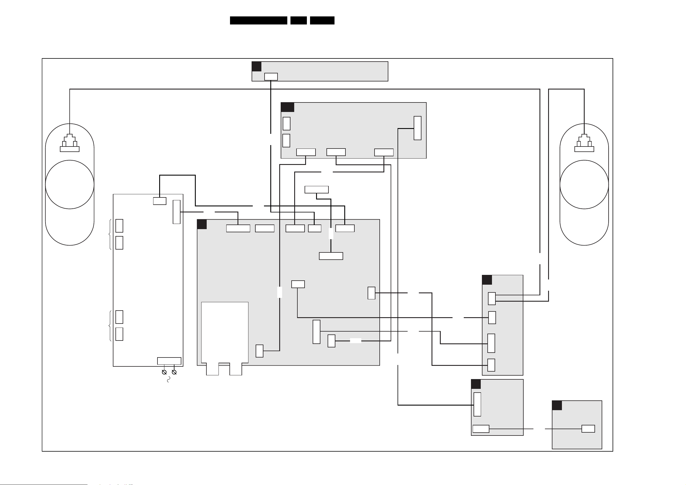
Wiring Diagram 15” 7
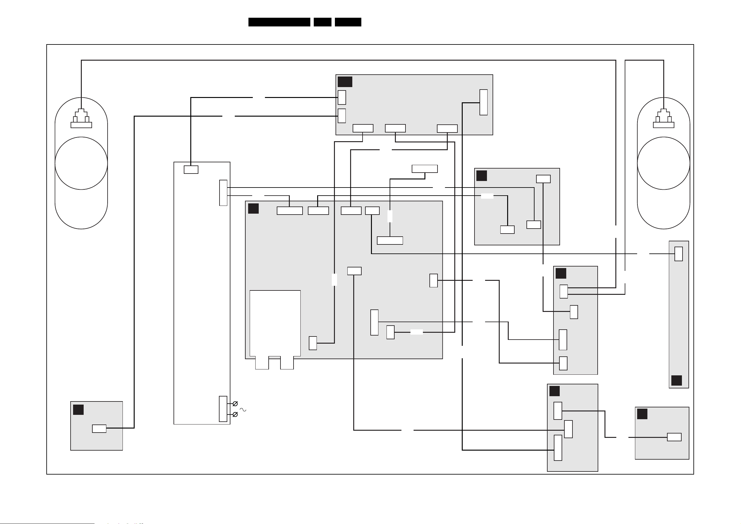
Wiring Diagram 20” & 23” 8
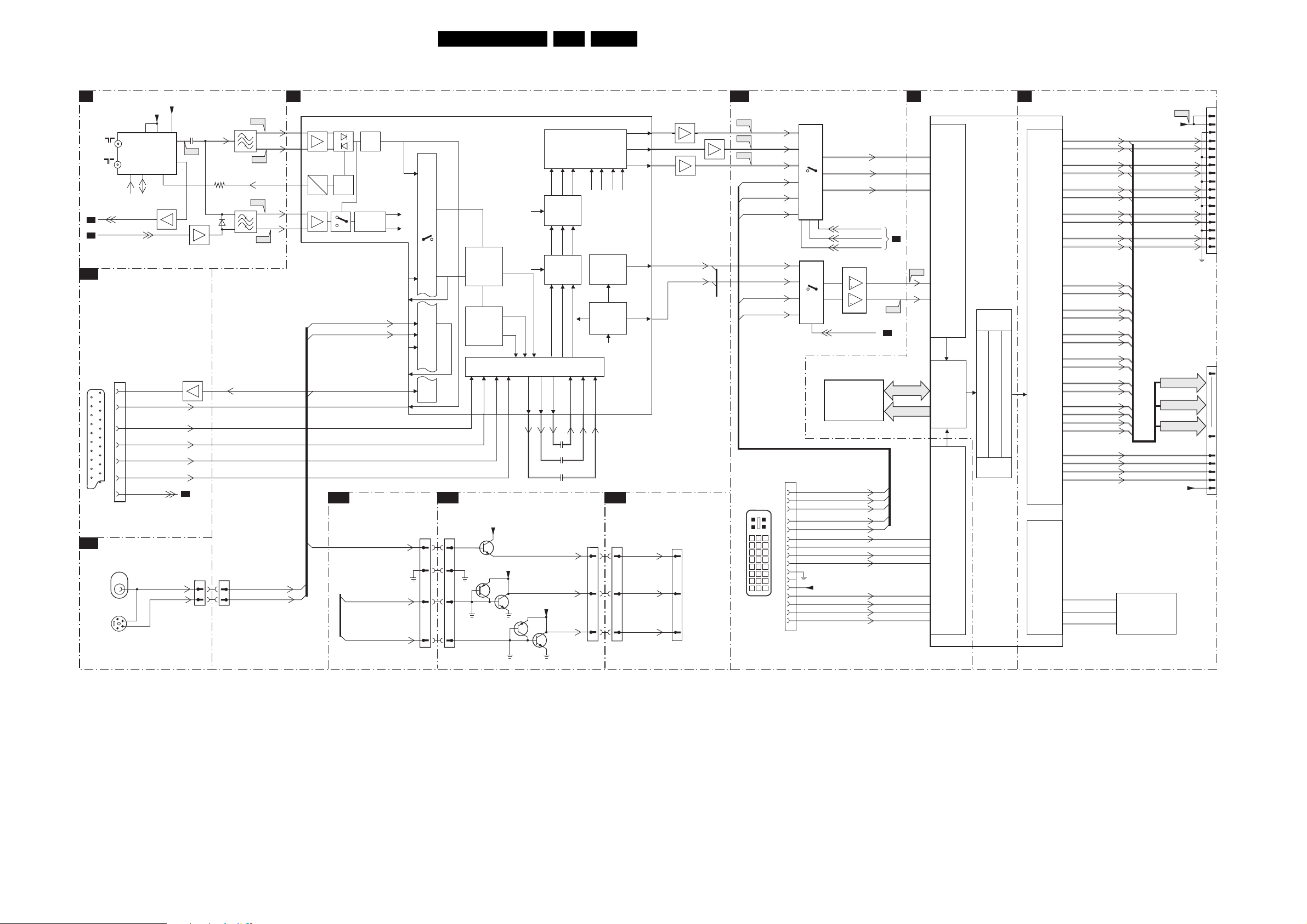
Block Diagram Video 9
Block Diagram Audio & Control 10
Testpoint Overview SSB (Top Side) 11
Testpoint Overview SSB (Bottom Side) 12
I2C Overview 13
Supply Voltage Overview 14
7. Circuit Diagrams and PWB Layouts Diagram PWB
Side I/O Panel & LKB 15” (D)15 16
Side I/O & Panel & LKB 20” & 23” (D)17 18
i-Board Panel (HC)19 20
LED and IR Panel (J) 21 22
LCD Clock Panel (J)23
8. Alignments 25
9. Circuit Descriptions, Abbreviation List, and IC Data
Sheets 28
Abbreviation List 28
IC Data Sheets 28
10. Spare Parts List 29
11. Revision List 32
©
Copyright 2005 Philips Consumer Electronics B.V. Eindhoven, The Netherlands.
All rights reserved. No part of this publication may be reproduced, stored in a
retrieval system or transmitted, in any form or by any means, electronic,
mechanical, photocopying, or otherwise without the prior permission of Philips.
Published by WS 0572 Customer Service Printed in the Netherlands Subject to modification EN 3122 785 15790
Page 2
EN 2 LC4.1HE AB1.
Technical Specifications, Connections, and Chassis Overview
1. Technical Specifications, Connections, and Chassis Overview
Index of this chapter:
1.1 Technical Specifications
1.2 Connection Overview
1.3 Chassis Overview
Notes:
• Only information that is related to the iTV module, is
published in this manual. For the other information, see the
relevant chassis manual (order code on front page).
• Some models in this chassis range have a different
mechanical construction. The information given here is
therefore model specific.
• Figures below can deviate slightly from the actual situation,
due to the different set executions.
• Specifications are indicative (subject to change).
1.1 Technical Specifications
1.1.1 Vision
Display type : LCD
Screen size : 15” (38 cm), 4:3
Resolution (HxV pixels) : 1024x768 (15”)
Contrast ratio : 500: 1 (15”)
Light output (cd/m
2
) : 450 (15” + 20”)
Response time (ms) : 16 (15” + 23”)
Viewing angle (HxV degrees) : 130x100 (15”)
Tuning system : PLL
TV Colour systems : PAL B/G, D/K, I
Video playback : NTSC
Supported computer formats : 640x480 (all)
Supported video formats : 640x480i-1fH (all)
Presets/channels : 125 presets
Tuner bands : VHF
: 20” (51 cm), 4:3
: 23” (58 cm), 16:9
: 640x480 (20”)
: 1366x768 (23”)
: 350 : 1 (20”)
: 450 : 1 (23”)
: 500 (23”)
: 25 (20”)
: 176x176 (20”)
: 140x125 (23”)
: SECAM B/G, D/K, L/L’
: PAL
: SECAM
: 720x400 (15”+23”)
: 640x480 (15” + 23”)
: 832x624 (15” + 23”)
: 800x600 (15” + 23”)
: 1024x768 (15” + 23”)
: 1280x768 (23”)
: 640x480p-2fH
(15”+23”)
: 720x576i-1fH (all)
: 720x576p-1fH (all)
: 1280x720p-3fH
(15”+23”)
: 1920x1080i-2fH
(15”+23”)
: UHF
: S-band
: Hyper-band
: FM-radio
1.1.2 Sound
Sound systems : FM-mono
: AM-mono
: FM-stereo B/G
: NICAM B/G, D/K, I, L
: AV Stereo
: Virtual Dolby
Surround
Maximum power (W
) : 2 x 2 (15”)
RMS
: 2 x 5 (20” + 23”)
1.1.3 Miscellaneous
Power supply:
- Mains voltage (V
) : 90 - 240 (15”+ 23”)
AC
: 100 - 250 (20”)
- Mains frequency (Hz) : 50 / 60
Ambient conditions:
- Temperature range (°C) : +5 to +40
- Maximum humidity : 90% R.H.
Power consumption (values are indicative)
- Normal operation (W) : ≈ 42/55/92
- Stand-by (W) : < 1/1.5/3
Dimensions (WxHxD cm) : 47.2x30.8x7.65 (15”)
: 58.3x38.6x8.7 (20”)
: 71.6x37.5x9.8 (23”)
Weight (kg) : 5 (15”)
: 8.5 (20”)
: 8.8 (23”)
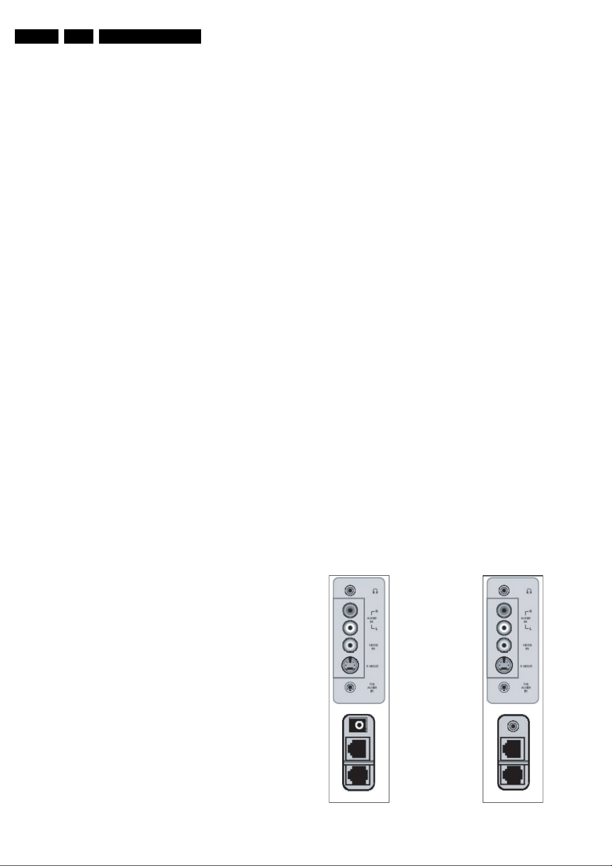
1.2 Connection Overview
Note: The following connector colour abbreviations are used
(acc. to DIN/IEC 757): Bk= Black, Bu= Blue, Gn= Green, Gy=
Grey, Rd= Red, Wh= White, and Ye= Yellow.
1.2.1 Side Connections
F_15790_002.eps
211105
F_15790_003.eps
Figure 1-1 Side I/O: 15” (left side), 20”+23” (right side)
211105
Page 3
Safety Instructions, Warnings, and Notes
EN 3LC4.1HE AB 2.
Mini Jack: Audio Head phone - Out
Bk - Head phone 32 - 600 ohm / 10 mW ot
Cinch: Video CVBS - In, Audio - In
Ye -Video CVBS 1 V
Wh - Audio L 0.5 V
Rd - Audio R 0.5 V
/ 75 ohm jq
PP
/ 10 kohm jq
RMS
/ 10 kohm jq
RMS
Mini Jack: DVI-Audio - In
1 -Ground Y Gnd H
2 -Ground C Gnd H
3 - Video Y 1 V
4 - Video C 0.3 V
/ 75 ohm j
PP
/ 75 ohm j
PP
S-Video (Hosiden): Video Y/C - In
1 - Ground Y Gnd H
2 - Ground C Gnd H
3 - Video Y 1 V
4 - Video C 0.3 V
- In (15-inch models)
12V
DC
1 - Supply +12 V
2 - Ground Gnd H
/ 75 ohm j
PP
/ 75 ohm j
PP
j
DC
3-n.c.
Mini Jack: Speaker - Out (20 + 23-inch models)
- Loudspeaker 8 ohm ok
RJ45: DATA2 (Xpress Box- In/Out)
1 - +12V +12 V / 1 W k
2 - GND Gnd H
3-H
4-V
Signal k
SYN
Signal k
SYN
5 - TXD232 Signal
6 - RXD232 Signal
7 - SDA3_IR-OUT Signal k
8 - DCM-POR Signal k
9 - CVBS-terr Signal k
10 - GNDA Gnd H
RJ12: DATA1 (HM-Link - In/Out)
1 - LED_in < 0.3 V, active low j
2 - IR_in < 0.3 V, active low j
3-MODE Vcc j
4 - TV Power Status 4.5 to 5 V - TV “On”, < 0.3V -
TV “Stdby”, High impedance -
TV “Off” k
5 - GND Gnd H
6 - IR_out Signal k
1.2.2 Rear I/O connections
Rear connections are the same as for the LC4.1E.
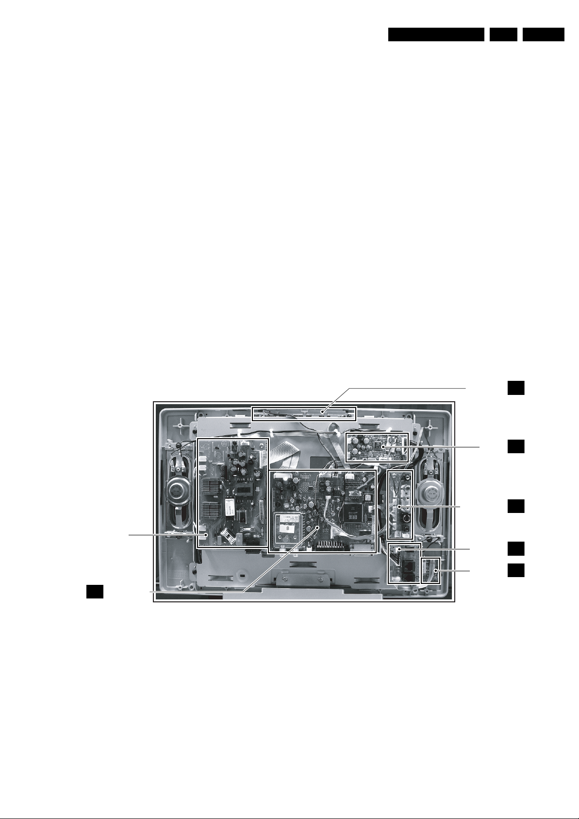
1.3 Chassis Overview
POWER SUPPLY
PA NE L
SMALL SIGNAL
B
BOARD
TOP CONTOL
PANEL
i-BOARD
SIDE I/O PANEL
iTV SIDE I/O
PA NE L
iTV LED & IR
PA NE L
F_15790_005.eps
E
HC
D
D
J
061205
Figure 1-2 PWB locations (depending on model)
2. Safety Instructions, Warnings, and Notes
See the relevant chassis manual (order code on front page).
3. Directions for Use
See the relevant chassis manual (order code on front page).
Page 4
EN 4 LC4.1HE AB4.
Mechanical Instructions
4. Mechanical Instructions
Index of this chapter:
4.1 Service Position
4.2 Cable Dressing
4.3 Assy/Panel Removal
4.4 Set Re-assembly
Notes:
• Only information that is related to the iTV module, is
published in this manual. For the other information, see the
relevant chassis manual (order code on front page).
• Figures below can deviate slightly from the actual situation,
due to the different set executions.
• Follow the disassembling instructions in described order.
Note: To diagnose the set with ComPair it is not needed to
open the set entirely.
To access the ComPair connector, proceed with the following:
1. Manually unlock and remove the cover cap.
2. Remove the tape shielding that covers the ComPair
connector (1).
Note: Make sure that both the ComPair connector and the
UART connector are shielded off with a piece of insulating tape
after repair for ESD reasons. Place this tape over the holes in
the rear cover of the set.
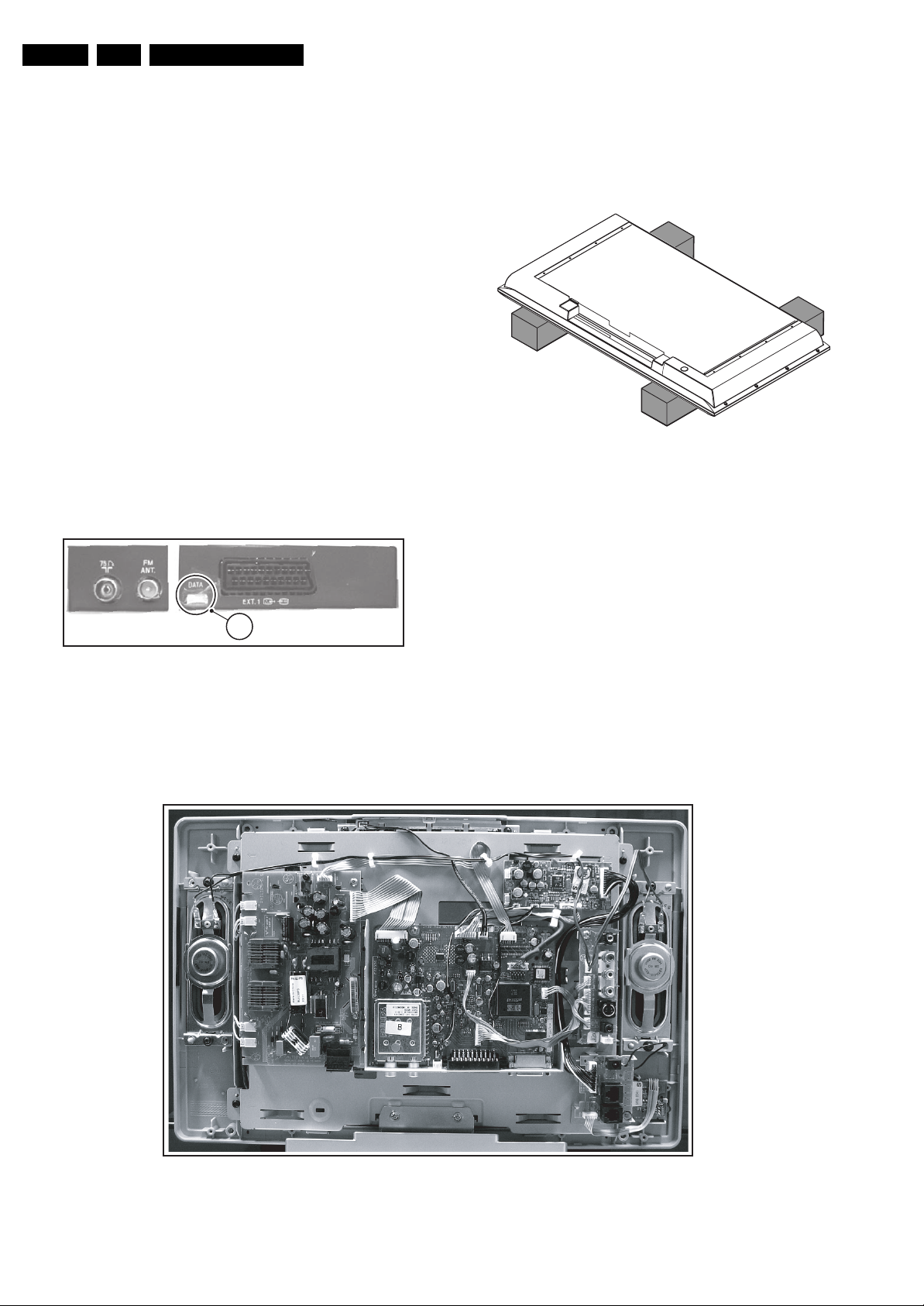
4.1 Service Position
4.1.1 Foam Bars
Figure 4-2 Foam bars
The foam bars (order code 3122 785 90580) can be used for
all types and sizes of Flat TVs. By laying the plasma or LCD TV
flat on the (ESD protective) foam bars, a stable situation is
created to perform measurements and alignments. By placing
a mirror under the TV, you can easily monitor the screen.
E_06532_018.eps
170504
Figure 4-1 ComPair connector
4.2 Cable Dressing
1
E_14520_034.eps
160904
Figure 4-3 Cable dressing (15-inch model)
F_15790_004.eps
051205
Page 5
Mechanical Instructions
EN 5LC4.1HE AB 4.
4.3 Assy/Panel Removal
4.3.1 Rear Cover
Warning: Disconnect the mains power cord before you remove
the rear cover.
1. Remove the screws that secure the rear cover.
2. Lift the rear cover from the cabinet cautiously. Make sure
that wires and other internal components are not damaged
during cover removal.
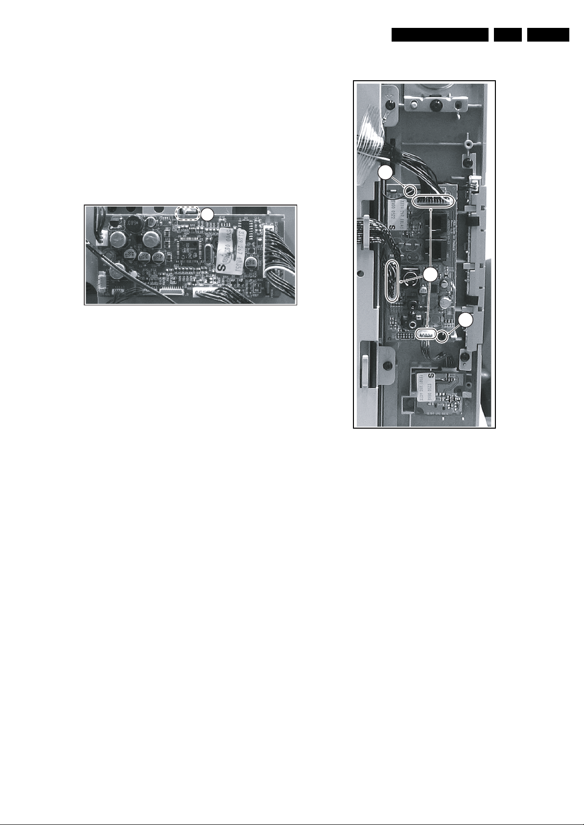
4.3.2 i-Board Panel
1
Figure 4-4 i-Board panel
F_15800_004.eps
201205
4.3.3 Side I/O Panel
2
1
2
1. Disconnect all cables from the panel.
2. Untwist the fixation lip [1] c.c.w. with a pair of pliers.
3. Remove the panel.
F_15800_005.eps
071205
Figure 4-5 Side I/O panel
1. Disconnect the cable [1] from the panel.
2. Release the two fixation clamps [2] and lift the panel out of
the bracket.
4.4 Set Re-assembly
To re-assemble the whole set, execute all processes in reverse
order.
Notes:
• While re-assembling, make sure that all cables are placed
and connected in their original positions. See Figure "Cable
dressing". Also make sure that the anti-static copper foils
are not damaged and that they make good electrical
contact with the metal frame. Be careful with the fragile
LVDS cable.
Page 6

EN 6 LC4.1HE AB5.
Service Modes, Error Codes, and Fault Finding
5. Service Modes, Error Codes, and Fault Finding
See the relevant chassis manual (order code on front page).
Personal Notes:
E_06532_012.eps
131004
Page 7
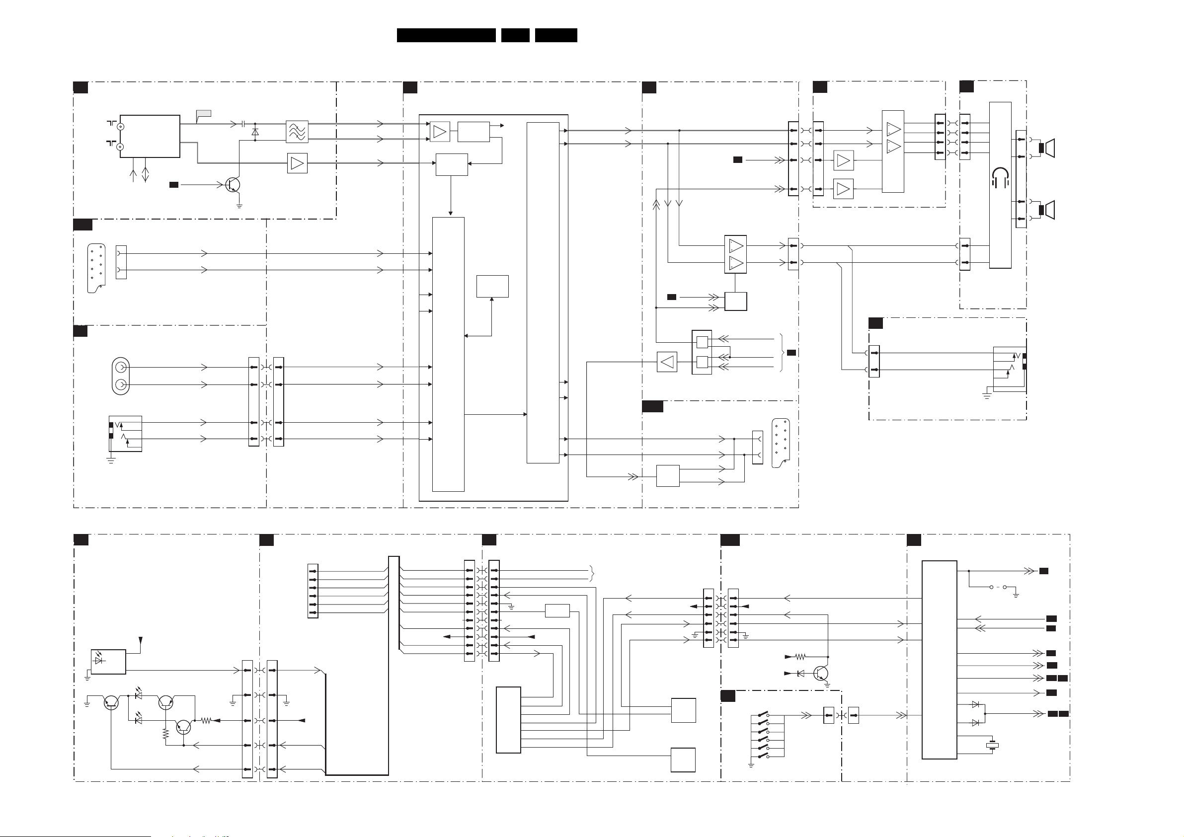
Block Diagrams, Test Point Overviews, and Waveforms
6. Block Diagrams, Test Point Overviews, and Waveforms
Wiring Diagram 15”
Wiring 15”
RIGHT
SPEAKER
TOP CONTROL
E
1684
3P
HC
8684
3P
4P
7LC4.1HE AB 6.
I BOARD
J10
J1
J2
4P
8408
LVDS CONNECTOR
TO DISPLAY
20P
J3
5P
J6
8P
24P
J4
LEFT
SPEAKER
5P
CN1
12P
1200
2P3
1360
TO DISPLAY
2P3
1362
B
8910
SSB
12P
1910
POWER
SUPPLY
8951
5P
1751
8P
1007
3P
1684
20P
1404
8404
5P
1951
8105
+
8403
1701
3P
1010
10P
1462
5P
8462
1401
4P
8401
8701
8010
8406
INVERTER
2P3
1365
TUNER
TO DISPLAY
2P3
1367
POWER IN
1001
2P
1332
4P
SIDE I/O
D
4P
1105
3P
10P
4P
8105
1110
1108
1111
ITV SIDE
i2
IO FOR C2
24P
1001
1540
5P
8870
ITV IR
J
MODULE
1540
5P
F_15790_006.eps
061205
Page 8
Block Diagrams, Test Point Overviews, and Waveforms
Wiring Diagram 20” & 23”
WIRING 20” AND 23”
8LC4.1HE AB 6.
HC
I BOARD
RIGHT
SPEAKER
3P
1260
POWER
SUPPLY
+
INVERTER
1200
8405
12P
B
8400
8910
SSB
12P
1910
5P
1751
8403
3P
4P
1007
J10
J1
8P
1701
3P
J2
4P
1684
3P
J3
5P
8408
8404
20P(40P)
1404(1402)
LVDS CONNECTOR
TO DISPLAY
20P(40P)
(8402)
1401
8910
4P
J8
6P
J4
24P
THE NUMBERS BETWEEN ( )
ARE FOR THE 20” DISPLAYS
AUDIO
I
AMPLIFIER
8751
8401
5P
1704
1706
5P
2P
1703
8107
SIDE I/O
D
4P
1105
8105
8105
LEFT
SPEAKER
8684
3P
1684
CLOCK
O
MODULE
4P
J1
1001
POWER IN
2P
TUNER
1332
4P
1010
10P
1462
5P
8409
8462
8406
8010
10P
4P
ITV SIDE
i2
IO FOR C2
5P
1540
24P
1001
1108
1111
3P
5P
1701
1107
8870
ITV IR
J
MODULE
F_15790_007.eps
TOP CONTROL
E
1540
5P
061205
Page 9
Block Diagrams, Test Point Overviews, and Waveforms
Block Diagram Video
VIDEO
TUNER + VIF
B1
TV IN
FM IN
B2
B2
REAR IO SCART
B10
SCART 1
1
21
EXT 1
SIDE AV
D
VIDEO
IN
5
S-VHS
1302
UR1316S
1101
19
20
16
15
11
1102
1101
1
2
SVHS
SSIF
SEL_IF
7
8
3
4
+VTUN
+5SW_a
67
TUNER
4
5
1
SCL
SDA
7316
CVBS_SC1_AV1_IN
SC1_FBL_IN
SC1_R_V_IN
SC1_G_Y_IN
SC1_B_U_IN
STATUS_1
AV3_CVBS_Y_IN
AV3_C_IN
9LC4.1HE AB 6.
HERCULES
B2
7011
F312
1328
7
2321
IF-TER
11
F306
7320
7101
EF
B2
1108
2
4
3311
6323
1010
2
4
2
1330
2
3
AV3_CVBS_Y_IN
VIF2
8
VIF1
F313
RF_AGC
F314
SIF2
7
SIF1
8
F315
SC1_CVBS_RF_OUT
AV3_C_IN
TDA15021H1
104
105
95
99
100
B8
B2
AC
DC
AV3_CVBS_Y_IN
ONLY FOR ITV SETS
B8
B2
B2
Sound
Traps
AGC
Detect
QSS Mixer
AM Demod.
AV3_C_IN
SYNC INTERFACE
SC1_CVBS_RF_OUT
H_CS_SDTV
CVBS1
QSS/FM
AM
V_SDTV
RGB Matrix
Blue & Black
Strech
Gamma Corr.
HC
J3
1
2
3
4
HERCULES
Dig. 2H/4H
Combfilter
Y Delay Adj.
Chroma
SECAM
Decoder &
Baseband
Delay
R/Pr-3
G/Y3
52 51 50 49
+5VA
Q2
+5VA
Q10
Q11
Uint
PAL/NTSC/
INSSW3
I-BOARD
SAT
SCAVEM
on text
Yint
Vint
RGB/Pr Pb Insert
YUV Interface
B/Pb-3
YOU T
UOUT
55 54 53 59 58 56
CVBSTERR
+5VA
Q8
Q9
Skin Tone
U/V Tint
Saturation
Peaking
SCAVEM
U/V Delay
VOUT
2057
2056
2027
HSYNC
VSYNC
YUV
YUV in/out
H/V
VIN
UIN
R_OSD
Vertical &
East-West
Geometry
Sync Sep
YSYNC
J4
13
8
9
G_OSD
H-OSC
H-Shift
H-Drive
Video
Switch
+
Control
c
cvbs/y
71
70
86
74
1462
1
2
3
4
RO
GO
BO
B_OSD
Fast Blanking
VDRB
HOUT
CVBS/Y
MODULE SIDE I/O
I2
1001
13
CVBSterr
8
HSYN
9
VSYN
44
43
42
107
62
7014
EF
7012
EF
V_SDTV
H_CS_SDTV
1003
9
3
TO SMART CARD
EXPRESS BOX
4
7013
For ITV
EF
only
B8
B8
SCALER I/O
B8
I044
R_SDTV
I041
G_SDTV
I039
B_SDTV
R_Pr_PC
G_Y_PC
B_Pb_PC
V_SDTV
H_CS_SDTV
HS_PC
VS_PC
C5
C1 C2
18
916
DVI-I
CONNECTOR
7461
27
3
7
25
1
5
21
22
7463
1
13
12
2
10,11
1485
27
26
25
28
8
C3 C4
1
24
2
9
10
11
14
+5VSWI
15
17
17
18
23
24
17
R_MUX
R_MUX
14
R_MUX
11
23
PC_HD_SEL
SD_PCHD_SEL
HD_FILTER
7510
14
1
15
5
SD_PCHD_SEL
7403
MX29LV040QC
SDRAM
1Mx32x4
B_Pb_PC
G_Y_PC
R_Pr_PC
HS_PC
VS_PC
RX2n
RX2p
RX1n
RX1p
RX0n
RX0p
RXCp
RXCn
4
CS_HSYNC
VSYNC
8
B7
F503
B7
RMDATA
RMADDR
B6
F499
SCALER
7401
GM5221H
151
147
142
181
182
INTERFACE
119
DVI/HDMI
118
124
123
129
128
132
133
ANALOG
INPUT
PORT
ROM
INPUT
PORT
SCALER
GRAPHIC
ZOOM
OUT BLENDER
OSD CONTROLLER
VIDEO
ZOOM
SCALER
B7
PAN_VCC
22
LV_E0_TX0-
21
LV_E1_TX0+
20
LV_E2_TX1-
LV_E3_TX1+
19
18
LV_E4_TX2-
17
LV_E5_TX2+
14
LV_E8_TX3-
LV_E9_TX3+
13
DISPLAY
16
15
38
37
36
35
34
33
32
31
30
29
43
44
45
46
47
48
49
55
93
92
84
LV_E6_TXC-
LV_E7_TXC+
LV_ O 0
LV_ O 1
LV_ O 2
LV_ O 3
LV_ O 4
LV_ O 5
LV_ O 6
LV_ O 7
LV_ O 8
LV_ O 9
PD20
PD21
PD22
PD23
FED
FHSYNC
FVSYNC
HSHCLK
SDA_IO
SCL_IO
WC
7
6
5
7402
M24C32
TIMING
GEN.
BRIGHTNESS/CONTRAST/HUE/SAT
SYSTEM
LV_E0_TX0-
EG1
LV_E1_TX0+
EG0
LV_E2_TX1-
ER7
LV_E3_TX1+
ER6
LV_E4_TX2-
ER5
LV_E5_TX2+
ER4
LV_E8_TX3-
ER1
LV_E9_TX3+
ER0
LV_E6_TXC-
ER3
LV_E7_TXC+
ER2
EB3
EB2
EB1
EB0
EG7
EG6
EG5
EG4
EG3
EG2
EB4
EB5
EB6
EB7
PAN _ V CC
EEPROM
(NVM)
4Kx8
F_15790_008.eps
F534
ER(0-8)
EG(0-8)
EB(0-8)
1404
1402
061205
1
2
5
3
4
7
6
8
9
10
12
15
18
TO DISPLAY (15” , 23”)
20
19
14
16
1
31
TO DISPLAY (20”)
33
35
37
39
42
Page 10
Block Diagrams, Test Point Overviews, and Waveforms
Block Diagram Audio & Control
AUDIO
TUNER + IF
B1
1302
TV IN
FM IN
REAR IO SCART
B10
1
21
EXT 1
SCART 1
SIDE AV
D
AUDI O
L/R IN
PC
AUDI O
IN
1104
UR1316S
1101
6
2
1102
TUNER
4
5
SCL
SDA
L_SC1_AV1_IN
R_SC1_AV1_IN
4
3
IFOUT
PC_AUDIO_L
PC_AUDIO_R
11
10
SEL_IF_SDM
B2
AV3_L_IN
AV3_R_IN
F306
IF-TER
7320
2321
6323
1108
10 10
1330
2
3
1010
66
77
99
7316
7
8
L_SC1_AV1_IN
R_SC1_AV1_IN
SIF2
SIF1
SIFF
AV3_L_IN
AV3_R_IN
PC_AUDIO_L
PC_AUDIO_R
HERCULES
B2
7217
TDA15021H
99
100
33
34
35
56
57
49
50
53
54
AD Conv.
Std Stereo
Decoder
AUDIO
SELECT
ADC/DAC
QSS Mixer
AM Demod.
AM
QSS/FM
I2S
Processor
10LC4.1HE AB 6.
AUDI O
CONTROL
Vol/Treb/
Bass
Features
DACs
61
60
62
63
36
37
AUDOUTLSR
AUDOUTLSL
OUT_MUTE
AUDIO AMPLIFIER
B4
STANDBY
B2
7752
REAR IO SCART
B10
SC1_L_RF_OUT
SC1_R_RF_OUT
7370
MUTE
MUTE
7602
74HC08PW
3
11
SC1_L
SC1_R
&
&
7712
TDA1517ATW
18
3
7702
7703
MUTE
1
2
12
13
STANDBY
B2
MUTE
FOR 20”, 23”
12,13
8,9
11
SOUND_ENABLE
POWER_DOWN
EXT_MUTE
1101
3
1
AUDIO AMPLIFIER
I
1751
1706
44
22
11
55
DISPLAY
1701
33
11
B2
1
21
EXT 1
SCART 1
AUDOUTLSR
AUDOUTLSL
7703-1
7703-2
7712
TDA1517ATW
14
7
9
8
SIDE AV
i2
1701
3
1
FOR 20”, 23”
DISPLAY
(20”, 23”)
19
16
2
5
R+
RL+
L-
(20”, 23”)
1704
44
55
11
22
D
1107
1110
FOR 15”
DISPLAY
SIDE AV
1106
HEAD
PHONE
1005
1001
4
3
SPEAKER
2
1
SPEAKER
BATHROOM
SPEAKER
RIGHT
LEFT
CONTROL
IR LED PANEL
J
6541
GND
7542
VS
OUT
+5VA
6540B
6540A
Green
Red
7540
3544
7541
3540
PC-TV-LED
IR
+5VA
LED-SEL
i2
1540
44
55
22
33
11
MODULE SIDE I/O
1002
1
2
To Smart Card
Express Box
1540
3
4
5
6
RC_IR
+5V
RD_GR_LED
LED_CTRL
LEDIN_CLK
IRIN_DATA-IN
MODE
STATUS_DATA-OUT
GND
IR_OUT
LEDIN_CLK
IRIN_DATA-IN
MODE
STATUS_DATA-OUT
GND
IR_OUT
LED_CTRL
+5V
RD_GR_LED
RC_IR
HC
1001
11
22
33
44
55
66
17 17
20 20
21 21
22 22
23 23
I-BOARD
J4
LEDIN_CLK_TXD_SCL1
IR_IN_DA
MODE
STATUS_DATA_OUT
IR_OUT
PC_TV_LED_OUT
LED_SEL_OUT
RC_IR
U5
P89C664
MICRO
CONTR.
+5V
9
18
13
11
1
10
40
TA-IN_RXD_SDA1
CONTR.
See Blockdiagram
I²C
PC_TV_LED
+3V3STBY
LED-SEL
IR_IN_TV
LIGHT-SENSOR
15
4
4
U4
HEF4053BT
MULTI
PLEX
U3
HEF4053BT
MULTI
PLEX
B3
1007
J6
66
55
44
33
22
71
E
Channel+
ChannelVol um e+
Vol um e-
HERCULES
+3V3STBY
+3V3STBY
+5VSW
PC-TV-LED
LED-SEL
3063
6060
KEYBOARD CONTROL
1309
KB
1310
1311
1312
Powe r
Menu
1313
1314
7060
1684
22
LIGHT-SENSOR
1684
KEYBOARD
HERCULES
B2
7011
TDA15021H1
SEL_IF
114
4015
107
HERCULES
IR
97
115
126
120
128
10
11
98
116
102
111
122
99
SERVICE
SOUND-ENABLE
6073
POWER_DOWN
6076
SDM
TV_IRQ
STATUS_1
EXT_MUTE
STANDBY
TV_SC_COM
1001
B1
B5
B3
B3
B3
B3
B4
B5
B4 B5
B3
F_15790_009.eps
061205
Page 11

Block Diagrams, Test Point Overviews, and Waveforms
Testpoint Overview SSB (Top Side)
11LC4.1HE AB 6.
X1
SERVICE TESTPOINT
F528 B6
F529 B6
F530 B5
F531 B5
F532 B5
F535 B6
F536 B5
F537 B6
F538 B6
F539 B6
I414 B5
I416 B5
I418 B5
I420 B5
I422 B5
X1
X1
500mV / div DC
5ms / div
3139 123 6019.1
F_15310_025.eps
270605
Page 12

Block Diagrams, Test Point Overviews, and Waveforms
Testpoint Overview SSB (Bottom Side)
12LC4.1HE AB 6.
3139 123 6019.1
F_15310_026.eps
270605
F002 C4
F003 B2
F004 A3
F005 D4
F006 D3
F007 E2
F009 A3
F013 B3
F014 B5
F015 B4
F017 A2
F018 A3
F020 B3
F021 B3
F022 B4
F023 C2
F026 C3
F029 D3
F034 D3
F040 D4
F041 D4
F042 D3
F043 D3
F044 D3
F045 D3
F050 A3
F051 A3
F099 B2
F101 E4
F102 E4
F103 E4
F104 E3
F105 E3
F106 E3
F107 E3
F108 E3
F109 E3
F110 E2
F111 E2
F112 E2
F113 E2
F114 E3
F115 E3
F116 E3
F301 E5
F302 E4
F303 D4
F305 D5
F306 D5
F307 D5
F308 E4
F309 D4
F310 B3
F311 D5
F312 C5
F313 C5
F314 C5
F315 C5
F401 D1
F402 D1
F403 C1
F404 C2
F405 C2
F406 C2
F407 C2
F408 D1
F409 C1
F410 C1
F411 C1
F412 C1
F413 C1
F414 B1
F415 B1
F416 C1
F417 C2
F455 C2
F456 C2
F457 C2
F471 E1
F472 D1
F473 D2
F474 E1
F475 E1
F476 E1
F477 D1
F478 E1
F479 E1
F480 E1
F481 E1
F484 E1
F485 E1
F487 E2
F489 D1
F497 D2
F498 E2
F499 C1
F501 D1
F502 D3
F503 C1
F504 D1
F505 D1
F506 E2
F507 E2
F533 B1
F534 B2
F707 B4
F708 A4
F710 A5
F751 D6
F752 D6
F753 C6
F903 A5
F904 A6
F905 A6
F906 A6
F907 A6
F908 A6
F909 A6
F910 A6
F911 B5
F912 C5
F913 B5
F914 A6
F951 A1
F952 A1
F954 B3
I005 B5
I008 D3
I009 B4
I011 D4
I015 B3
I016 D4
I017 B4
I018 B4
I019 B4
I020 B4
I022 C5
I034 D3
I035 D3
I036 D3
I039 D1
I040 C3
I041 D2
I043 D3
I044 D2
I046 D3
I047 D3
I048 D3
I049 D3
I051 D3
I052 D3
I053 D3
I055 C3
I056 B3
I057 D2
I058 C2
I059 C3
I060 C2
I061 C2
I062 C3
I063 B3
I064 B3
I067 C3
I068 B3
I069 D3
I070 C3
I071 B3
I082 D5
I091 C2
I093 B3
I094 B4
I096 B4
I098 A3
I101 E4
I102 E4
I103 E4
I104 E3
I105 E3
I106 E3
I107 E3
I108 E3
I109 E3
I110 E2
I111 E2
I112 E4
I113 D4
I114 E4
I115 D3
I116 E3
I301 D5
I302 D5
I303 D5
I304 D5
I306 D5
I307 D5
I308 D5
I310 D5
I401 D2
I402 D2
I403 C1
I404 C1
I405 D2
I406 D2
I407 D2
I408 D2
I410 C2
I411 C2
I412 C2
I413 A2
I419 A1
I438 B1
I451 B2
I462 D1
I463 D1
I464 D1
I483 E1
I484 E2
I485 E1
I486 E1
I487 E1
I488 E1
I492 C1
I493 C1
I494 C1
I496 C1
I512 D1
I513 D1
I514 D1
I516 D2
I517 E2
I518 D3
I701 A4
I705 A5
I706 B4
I707 A4
I708 A5
I709 B4
I710 B4
I711 A4
I714 A5
I715 B5
I719 B5
I720 A5
I721 B3
I722 A3
I751 C6
I752 D6
I753 D6
I901 B6
I902 C6
I904 B6
I905 A6
I906 B6
I907 B6
I908 C6
I909 A6
I910 B6
I911 B6
I912 B6
I951 B1
I952 A1
I953 A1
I954 A1
I955 A1
I956 B2
I957 A2
Page 13

Block Diagrams, Test Point Overviews, and Waveforms
I2C Overview
13LC4.1HE AB 6.
I²C
HERCULES
B2
7011
TDA15021H1
HERCULES
PROCESSOR
SET
SCALER
B7
+3V3STBY
3353
20
3354
21
ERR
6
25
NVM_WP
3356
+3V3STBY
3353
3097
56
7099
M24C16
EEPROM
7
NVM
ERR
9
SDA
SCL
3430
78 77
7401
GM5221
SCALER
ERR
4
3431
TUNER + IF
B1
+3V3_DVDD
3303
3302
54
1302
UR1316S
TUNER
ERR
10
1332
ITV
INTERFACE
1331
SDA
SCL
SERVICE
CONNECTOR
COMPAIR
HC
I-BOARD
J2
33
22
1
2
3
R26
R25
32
U5
P89C664
8 bit
MICRO
CONTROLLER
+5VD
R23
+5VD
TXD
RXD
R24
R39
R69
+5VD
13
11
12
R40
U3
HEF4053BT
MULTI
PLEXER
U7
ST202ECD
RS232
TRANCIEVER
R67
R68
14
14
13
TXD232
RXD232
J1
J4
24
10
11
SDA
SCL
SDA2
22
21
SCL2
23
SDA3
+5VD
RP1
RP1
SIDE I/O
i2
2
TO
CLOCK MODULE
3
(Optional)
1001
SDA3_IR-OUT
24
10
11
TXD232
RXD232
1003
7
5
6
EXPRESS BOX
TO SMART CARD
SCALER IO (OPTIONAL)
B8
C5
C3 C4
C1 C2
1485
24
7
6
18
916
17
DVI-D
CONNECTOR
SIDE I/O
D
+3V3STBY
1112
1
3
2
3123
3124
3497
3496
1111
11
22
33
44
56
M24C02
EEPROM
1401
SDA_DVI
SCL_DVI
7490
256x8
+3V3_DVDD
JTAG_SDA_UART_TX
JTAG_SCL_UART_RX
DCC_DVI_5V
3495
3514
+3V3_DVDD
3401
3402
3442
3441
3414
93
92
NVM_WPP
DATA
84
RMADDR
RMDATA
80
79
ADDRESS
72
71
3443
+3V3_DVDD
B6
3444
SCALER
SDA_IO
SCL_IO
5
7402
M24C32
7
EEPROM
ERR
7403
MX29LV040
FLASH
ROM
ERR
6
8
4
7
5
CLK_LED-IN_SCL1
43
DATA-IN_SDA1
44
SDA1
24
25
SCL1
TXD
RXD
Q12
12
U2
HEF4053BT
2
MULTIPLEX.
13
3
+5VD
RP5
R35
56
MC24C16
U8
15
14
RP5
R34
IR-IN_DATA-IN_
RXD_SDA1
LEDIN_CLK_
TXD_SCL1
2
2
IRIN_DATA-IN
1
1
LEDIN_SCL1
1002
2
1
EXPRESS BOX
TO SMART CARD
UART DOR
SERVICE
F_15790_011.eps
061205
Page 14
Block Diagrams, Test Point Overviews, and Waveforms
Supply Voltage Overview
SUPPLY LINE OVERVIEW
TV SUPPLY
1200
TO 1951
CN1
1260
I BOARD
(20”, 23”)
B5
1910
1
2
3
4
5
6
7
8
9
10
11
12
B9
SSB
(15”)
TO J10
HC
+12VSW
+12VSW
POWER_DOWN
STANDBY
BACK_LIGHT_A
LAMP_ON_OFF
5930
SUPPLY
PANEL
(PSU)
+
INVERTER
1001
7930
MC34063AD
3935
6
DJ1
SUPPLY
IC
14LC4.1HE AB 6.
TUNER + IF
B1
B5
F903
F905
F906
B2
B2
B7
B7
F913
5931
7936
3937
1
7920
IN OUT
COM
F912
5932
5932
6910
AUD_SUP
+3V3STBY
+12VSW
+5VSW
+VTUN
+8VSW_TV
B4
B1,B2,B3,
B4,B6,B8,
B9
B9
B1,B2,B3,
B4,B7,B8,
B10
B1
B2
B5
B5
B5
B5
B5
B3
B3
B5
B5
B5
B5
B5
B5
B9
+5VSW
+VTUN
+3V3STBY
HERCULES
B2
+3V3STBY
+5VSW
+8VSW_TV
+1V8_A
+1V8_B
HERCULES
B3
+5VSW
+3V3STBY
3001
3002
3003
3004
DECDIG
B2
AUDIO AMPLIFIER +PROCESSING
B4
AUD_SUP
+5VSW
+3V3STBY
SCALER
B6
+3V3STBY
5401
5404
+1V8
5402
5403
7001
7004
7003
7002
+5VSW
+VTUN
+3V3STBY
+3V3STBY
+5VSW
+8VSW_TV
+1V8_A
+1V8_B
+5VSW
+3V3STBY
1007
+1V8_A
+1V8_B
AUDIO_SUP
+5VSW
+3V3STBY
+3V3STBY
+3V3_AVDD
+3V3_DVDD
+1V8
+1V8_AVDD
+1V8_DVDD
5
(20”,23”)
1007
1260
PSU
SCALER
B7
+3V3_AVDD
+3V3_DVDD
+5VSW
PA N_VCC
+3V3STBY
VDD
+5VSW
DCC_DVI_5V
+3V3STBY
+1V8
PA N_VCC_IN
*SEE DIVERSITY LIST
L4
L5
L6
1540
PAN_VCC
15”
+5VSW
+3V3STBY
+3V3
+5V
+5VA
+5VD
+5V
+12V**
+12V
4,5
J1
J4
1200
PSU
12VDC
IN
(15”)
J4
HC
1540
i2
B6
1
1
21
7
HC
CN1
PSU
(15”)
B7
J1
1442
O
1001
i2
HC
B2
B2
B7
B7
J2
+3V3_AVDD
+3V3_DVDD
+5VSW
PAN_VCC
SCALER IO
B8
+3V3STBY
+5VSW
1485
6486
5
SUPPLY
B9
+3V3STBY
+12VSW
PA NEL_
POWER_
CTL
B9
REAR IO SCART
B10
+5VSW
I-BOARD
HC
J2
+3V3STBY
1
J10
+12V**
1
5956*
5955
6485
7954
L1
7952
5520
5485
U1
CONTR
7955
IN OUT
COM
5958*
5957* 5961
7953*
5959*
IN OUT
COM
D2
SMPS
+12V*
15”
B6
B6
B5
B9
B5
B5
B5
B5
B5
B3
AUDIO AMPLIFIER
I
1703
1
MODULE SIDE I/O
i2
1004
12V*
1
1001
12V*
7
21
ITV IR MODULE
J
1540
1
CLOCK BOARD
O
1442
1
*For 15” 12V Supply for I-Board is
comming from external supply
Module Side I/O (1004)
**For 20”, 23” 12V Supply for I-Board
is comming from PSU (1260)
15”
(OPTIONAL)
L1
AUD_SUP
1003
12V
1
12V**
+5V
1540
1
+5VA
VDDVDD
F_15790_010.eps
061205
1540
J
Page 15

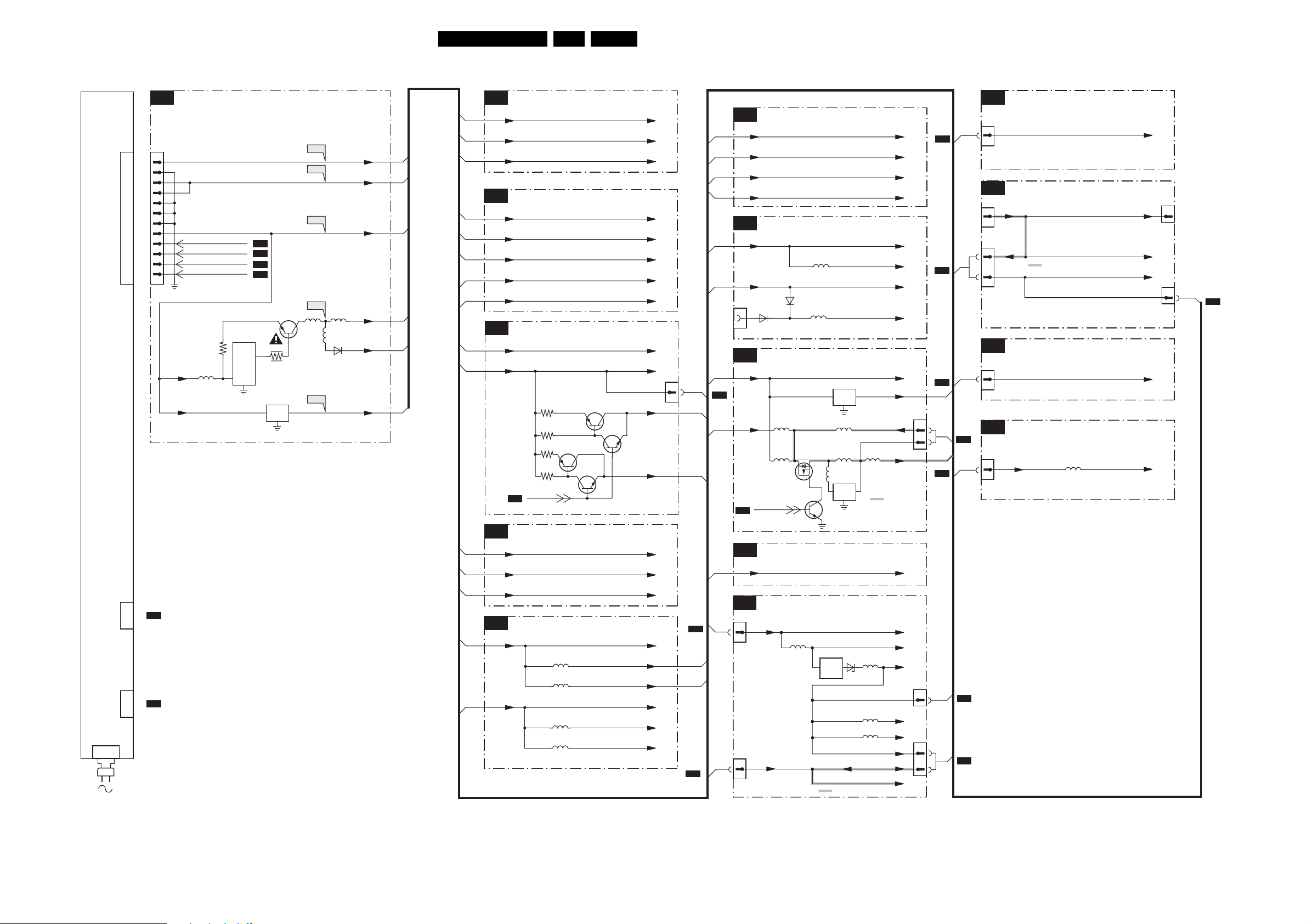
Circuit Diagrams and PWB Layouts
7. Circuit Diagrams and PWB Layouts
Side I/O Panel & LKB 15”
15LC4.1HE AB 7.
654321
SIDE I/O 15”
i2
D
3016
C
B
A
3139 123 5986.2
5K6 3018
1
2006
100nF
3017
5K6
MH1
MOUNTING_HOLE
1
2
34
1 2 3 4 56
1K8
3021 1K-NL
2005 4n7F
2
7007
BC857BW-1
3
3019
1K
3020
2K2
9
6
5
3022
1K5
23
7008
MH2
BC857BW-1
3023
560R
1
MOUNTING_HOLE
1
2
34
1
7006
BC857BW-NL
6006
BZX384-C5V1-NL
1009
1_PIN_CONN
9
6
5
1008
1_PIN_CONN
1004
TC18-041-03
3024
1K-NL
6004
23
AK
BZX384-C5V1-NL
2009
AK
1
1
3025
41.7R
+
3026
41.7R
3033
0R
3034
0R
L
N
-Fu2.2
12
7000
TCET110-3G
34
3031
10K
3032
10K
1
3
2
5005
5006
2003
2.2uF, 25V-NL
6002
BAS316
1
1
5002
10uH
6.8uH
6.8uH
2007
2U2
2002
100U,50V
2
1
PH 3112 338 3088
32
7001
BC847BW-1
3027
0R
3
7009
BC847BW-1
2
1002
6PIN-CONN
6011
PRLL4001
12V HSYN
+
45001
3
3035
1K
6001
BAS316
2010
100pF
2004
+
1000uF,16V
3028
2.2K
3029
220R
BZX384-C10
6005
3030
1K
3007
10R, 0805
3008
10R, 0805
6012
PRLL4001
10PIN-CONN
AK
4
2
1
2
3
RJ12
4
5
6
1
2
3
4
5
RJ45
6
7
8
9
10
1003
3
5000
LITAI 320417-3
1
456
1733
SPPH4
123
MODE_12V
1
2
3
6009
BZA408B
TV_12V
VSYN
TXD232
RXD232
DCM-POR
CVBSterr
GNDA HP-ROUT
1
2
3
4
1
2
3
4
1007 4B-PH-K-S
6
5
4
6010
BZA408B
1
2
3
SDA1
1005
LGT1509-0200
1006
4B-PH-K-S
R+
R-
TO TV Board
L+
L-
R+
R-
TO LoudSPK
L+
L-
6007
3036
Res, 0603
4
6V5C-483XZB
AK
6
5
4
123
6V5C-483XZB
6008
AK
2008
2n2
5003
6.8uH
5004
6.8uH
LEDIN_SCL1
IRIN_DATA-IN
MODE_12V
STATUS_DATA-OUT
DGND
IR OUT
TV_12V
HSYN
VSYN
TXD232
RXD232
DCM-POR
CVBSterr
GNDA
PEND IR
LED_CTRL
+5V
RD_GR_LED
RC_IR
3
2
HP-LOUT
1
10
11
12
13
14
15
16
17
18
19
20
21
22
23
24
1701
3B-PH-K-S
1
2
3
4
5
6
7
8
9
1
2
3
4
5
TO i-BOARD
B24B-PHDSS-B
1540
5B-PH-K-S
TO IR MODULE
TO SSB
B
F_15790_012.eps
HC
1001
J
D
C
B
A
071205
Page 16

Circuit Diagrams and PWB Layouts
Layout Side I/O Panel 15” (Top Side)
16LC4.1HE AB 7.
Personal Notes:
3139 123 5986.2
Layout Side I/O Panel 15” (Bottom Side)
F_15790_013.eps
061205
3139 123 5986.2
F_15790_014.eps
061205
E_06532_012.eps
131004
Page 17

Circuit Diagrams and PWB Layouts
Side I/O & Panel & LKB 20” & 23”
17LC4.1HE AB 7.
654321
SIDE I/O 20” & 23”
i2
D
3016
C
B
A
3139 123 6159.1
5K6
2006
100nF
MOUNTING_HOLE
1
3017
5K6
MH1
1
2
3 4
123456
3018
1K8
3021 1K-NL
2005 4n7F
23
7007
BC857BW-1
3019
1K
3020
2K2
9
6
5
4003
1 2
JUM PER
4004
1 2
JUM PER
4005
1 2
JUM PER
4006
1 2
JUM PER
4008
1 2
JUM PER
4009
1 2
JUM PER
4010
1 2
JUM PER
9001
1 2
JUM PER
3022
1K5
2
1
MOUNTING_HOLE
7008
BC857BW-1
3
3023
560R
MH2
1
2
3 4
9
6
5
1
23
7006
BC857BW-NL
6006
BZX 384-C5V 1-NL
1009
1_PIN_CONN
1008
1_PIN_CONN
3024
1K-NL
6004
A K
BZX 384-C5V 1-NL
2009
A K
1
1
uF-N L
2
2.
3 4
1004
TC18-041-03
3025
41.7R
3026
41.7R
3033
0R
3034
0R
12
3031
10K
3032
10K
1
3
2
5005
5006
2003
2.2uF, 25V-NL
+
7000
TCET110-3G
6002
BA S316
1
1
5002
10uH
6.8uH
6.8uH
2007
2U2
2002
100U,50V
2
1
PH 3112 338 3088
3
7001
BC847BW-1
2
3027
0R
+5V
3037
10K
32
7009
BC847BW-1
1002
1
2
6PIN-CONN
4002
JUM PER
6012
PRLL 4001
12V
1003
10PIN-CONN
3
5000
LITA I 320417-3
1
5
6
4
123
3
4
5
6
1
2
3
4
5
6
7
8
9
10
1733
SPPH4
RJ12
4001
1 2
JUM PER
6011
PRLL 4001
12V HSYN
+
45001
3
3035
1K
6001
BA S316
2010
100pF
2004
+
1000uF,16V
3028
2.2K
3029
220R
BZX 384-C10
6005
3030
1K
10R, 0805
10R, 0805
9003
1 2
JUM PER
AK
3007
3008
1 2
RJ45
4
2
MODE_12V
4007 0R
6009
1
2
3
BZA408B
GNDA HP-ROUT
6
5
4
TV_12V
VSYN
TXD232
RXD 232
DCM-POR
CVBSterr
6010
BZA408B
1
2
3
SDA1
1005
LGT1509-0200
1006
4B-PH-K -S
1
R+
2
R-
TO TV Board
3
L+
4
L-
1
R+
2
R-
TO LoudSPK
3
L+
4
1007 4B-PH-K -S
L-
2
3036
Res, 0603
6
5
4
4
3
6007
6008
A K
1
A K
BZX 384-C5V 6
BZX384-C5V6
2008
2n2
4011
JUM PER
5003
6.8uH
5004
6.8uH
12
LEDIN_SCL1
IRIN_DATA-IN
MODE_12V
STATUS_DA TA -OUT
DGND
IR OUT
TV_12V
HSYN
VSYN
TXD232
RXD 232
DCM-POR
CVBSterr
GNDA
PEND IR
LED_CTRL
+5V
RD_GR_LED
RC_IR
9002
JUM PER
HP-LOUT
SDA1
12
1701
3
2
1
3B-PH-K -S
1
2
Trd
3
TO i-BOARD
4
5
6
7
8
9
B24B-PHDSS-B
10
11
12
13
14
15
16
17
18
19
20
21
22
23
24
1
1540
5B-PH-K -S
2
3
TO IR MODULE
4
5
TO SSB
B
F_15790_015.eps
HC
1001
J
D
C
B
A
071205
Page 18

Circuit Diagrams and PWB Layouts
Layout Side I/O Panel 20” & 23” (Top Side)
18LC4.1HE AB 7.
3139 123 6159.1
Layout Side I/O Panel 20” & 23” (Bottom Side)
F_15790_016.eps
061205
3139 123 6159.1
F_15790_017.eps
061205
Page 19

i-Board Panel
Circuit Diagrams and PWB Layouts
19LC4.1HE AB 7.
654321
HC
J10
D
C
B
A
3P-CONN-PH-B
J1
LCD Clock
4P-CONN-T YCO
J7
5P-CONN-T YCO
J4
To Side
I/O
24P- CONN-PHDSS-B
SR
To TV
BD
5P-CONN-SR-V
SR
To TV
BD
4P-CONN-SR-V
Fr om TV
SR
LC04V
10P- CONN-SR-V
SR
LC04C
8P-CONN-PH-V
3139 123 6133.3
i-BOARD
1
2
3
4
3
2
1
5
4
3
2
1
1
2
3
4
5
6
7
8
9
10
11
12
13
14
15
16
17
18
19
20
21
22
23
24
J3
1
2
3
4
5
J2
4
3
2
1
J5
1
2
3
4
5
6
7
8
9
10
J6
1
2
3
4
5
6
7
8
R87
NFR254R7
LCM_POW
SCL2
SDA2
LEDIN _CLK_TXD_SCL1
IR-IN_DATA-IN_RXD_SDA1
MODE
STA TU S_DA TA _OUT
GND
IR_OUT
+12V
HSYNC
VSYNC
TXD232
RXD232
DCM_POR
CVBSTER R
GNDA
HP_ROUT_ RC-PULL UP
HP_LOUT
KEYBOARD_TV INTP
PEND _IR
PC_T V_L ED_ OUT
L10 6u8- 1008
LED_SEL_OUT
RC_IR
R70 100R
R7
100R
Q2
BC847BW
GNDA
+3V3ST BY
HP_ROUT_ RC-PULL UP
HP_LOUT
PC_T V_L ED
LED_SEL
GND
+3V3S
LI GHT SEN SOR
IR_IN TV
KEYBOARD_TV INTP
P50_IT V
IR_IN TV
LED_SEL
PC_T V_L ED
LI GHT SEN SOR
P50_IT V
+3V3ST BY+12V +3V3
L1
6u8
U9 LED50CZ
3
IN
OUT
GND
2
L7 Ferrit ebe ad
C7 100nF
+12V
GNDA
+5V
+5VA
R9
C8
220R
100nF
3
1
2
R38
220R
HSYN
VSYN
SDA
SCL
+3V3S
R71
0R
1
R84
0R
+
C1
220uF, 16V
Q14
PBSS5140U
3
2
R73
4K7
+5V
R10 100R
R11 100R
R74 100R
R13 100R
R16 100R
R43
0R
CVBSTER R
R8
68R
HP_ROUT _RC-PULLUP
IR_IN TV
LED_SEL
R49 1 R5
R50
1R5
C38
27pF
R72
1
1K
VSYN
C29
10uF
C39
27pF
3
2
BC847BW
R81 0R
+5VA
Q4
R76
10K
1
+5VA
32
L3
68uH
R2
220R
R4
1K0
SCL2
SDA2
LCM_POW
R75 0R
R18
1K0
R82
10K
1
Q15
BC847BW
+5VD
L6
6.8uH - 1008
+ C6
+5VA
U1
MC34063AD
8
Drive
Sw it ch
Coll ecto r
Coll ecto r
7
IpkSense
Sw it ch
Emit t er
6
Vcc
Timing
Capacit or
5
Comparat or
Ground
Inv. I/p
R5
2K7
C40 1nF
K
+5VA
Q3
BC857BW
1
R15 10
R17
150R
+5VA
C11 100nF
6
U3
1
14
dd
Za
Y1a
V
Y0a
15
Zb
Y1b
Y0b
4
Zc
Y1c
Y0c
11
Sa
Vss
10
Sb
Vee
9
Sc
HEF4053BT
R19
+5VA
10K
Q5
32
BC847BW
1
R83
1K
+5VA
R52
47K
Q8
BC857BW
2
R53
47K
1
R51
10K
R85
10K
3
R54
10K
D2
SS24
1
A K
2
C2
3
4
100pF
R6
470R
2
3
13
12
1
2
RJI R_IN
Tristate
3
5
8
7
6
E
R20
10K
1
R48
22K
U4
14
Za
15
Zb
4
Zc
11
Sa
10
Sb
9
Sc
HEF4053BT
R55
4K7
32
Q9
BC847BW
10uF
IRIN _DATA-IN
14
Za
15
Zb
4
Zc
11
Sa
10
Sb
9
Sc
HEF4053BT
+5VA
16
R3
100R
R14
2K2
R12
10K
L4
6.8uH
C28
+ C3
220uF, 16V
+5VA
C9
100nF
U2
16
dd
Y1a
V
Y0a
Y1b
Y0b
Y1c
Y0c
Vss
Vee
E
STATUS_DATA_OUT 1
C12 100nF
13
dd
Y1a
V
12
Y0a
1
Y1b
2
Y0b
3
Y1c
5
Y0c
8
Vss
7
Vee
6
E
1
T
EL_OU
S
LED_
L5
6.8uH - 1008
+5V
6
+ C4
D3
13
12
1
2
3
5
8
7
6
SDA3
PEND _IR
RC_IR
32
Q1
BC847BW
220uF, 16V
BZX384-C5V
W
D
X
TXD
R
LUP_S
L
U
P
IR_
+5V
L8
6.8uH - 1008
100uF, 16V
Q12
1
BC847BW
R28
10K
SYN C
V
32
LCM_POW
HSYN
R27
10K
+
C5
100uF, 16V
R56
10K
R86
10K
100uF, 16V
L14
BLM21P221SN1D
+C26
+5VD
8
2 7
3 6
1
R1
100R
Q10
BC857BW
1
4 5
R57
47K
C33
10nF
C34
10nF
C27
100nF
RP1
10K-RP
23
R59
10K
10K-RP
C13 27pF
C14 27pF
+5VA
R58
47K
1
SDA1
SCL1
+5VD
C42
100nF
+5VD +5VD
SPAREIO
J9
1 8
2 7
364 5
CLK_ LED- I N_SCL1
DATA-IN_SDA1
LIGHT SENSOR
SCLS
TV_POR
Q11
BC847BW
3P-CONN-SR-V
1
2
C30
10nF
C32 10nF
+5VD
R25 100R
R26 100R
IB_IROUT
RP2
A
D
R60
4K7
32
U8
5
SDA
6
SCL
7
WC
8
VCC
MC24C16
3
R80
SR
10K
C31
10nF
34
35
36
37
38
39
40
41
42
43
44
R77 10K
R23
4K7
R29
2K2
+5VD
C43
1uF
4
VSS
3
E2
2
E1
1
E0
1 8
33
P0.4 /A D4
P0.3 /A D3
P0.2 /A D2
P0.1 /A D1
P0.0 /A D0
VCC
NIC*
P1.0 /T 2
P1.1 /T 2EX
P1.2 /EC I
P1.3 /CEX 0
P1.4 /CEX 1
2
CEX
5/
P1.
1
R24
4K7
C37
10nF
L13
7
2
32
2
BLM21P221SN1D
6
RP3
10K-RP
4 5
3
8
0
1
2
3
3
29
p
*
7
5
p
D
IC
AD
/
N
5
.7/A
.
EA/V
0
0.6/A D6
P
P
P0
L
D
x
DA
S
*
0/R
7/
T
.6/SC
.
S
P1
P1
R
P3.
NIC
4
3
5
6
780R
R
D
X
R
3
2
R63
47K
R64
10K
R79 10K
27
26
ALE
PSEN
D
x
1/T
.
P3
P3.2/INT0
8
7
R
I
_
RC
TXD
Q6
BC847BW
1
C15
1uF
C35 10nF
4
25
2
5
14
A
6/
7/A 1
.
P2.
P2
P2.4 /A 12
P2.3 /A 11
P2.2 /A 10
P2.1 /A9
P2.0 /A8
XTAL1
XTAL2
P3.7 /R D
P3.6 /W R
/T0
3
X
CE
.3/INT1
3
P
P3.4 /
9
0
1
ED
L
_
_TV
PC
C18
100nF
23
3
1
A
/
.5
P2
22
21
20
19
18
17
NIC*
16
VSS
15
14
13
12
T1
4/
EX
C
5/
.
P3
U5
11
P89C664HBBD
R42
0R
R31
22K
1
C41
Reserve
C45
10nF
+5V
IB_IROUT
R32
22K
32
Q13
BC847BW
HSYNC
C44 100nF
L12
6u8- 1008
100uF, 16V
TXD232
RXD232
R21
100R
R44
10K
R
DCM_PO
C22
C19 100nF
C20 100nF
R62 100R
R61 100R
3
A
SD
R69 10K
R22 1K
X1
16MHz
D
X
RXD
T
+
C21
100nF
2
V+
6
V-
14
T1_OUT
7
T2_OUT
13
R1_IN
8
R2_IN
+5VD
R33 100R
R34 100R
R35 100R
RP5
1 8
2 7
3 6
4 5
10K-RP
C16 27pF
C17 27pF
+5VD
RP4
4 5
3 6
2 7
1 8
10K-RP
SW1
1 2
Tact Sw itch, SKQNABD010
R30
5K6
16
C
VC
R1_OUT
R2_OUT
GND
ST202ECD
15
+5VD
+5VD
U6
DS1813
RST1VCC
D
N
G
3
T1_IN
T2_IN
C1+
C1-
C2+
C2-
+5VD
2
U7
1
3
4
5
11
10
12
9
32
BC847BW
R40
4K7
R36 100R
+5VD
C24 100nF
C23 100nF
R37 100R
J8
1 2
Q7
2P-Shrouded-HDR
1
R46 4K7
R47
4K7
R39
4K7
R67
100R
R68
100R
L11
6.8uH - 1008
C25
1uF
DGND
C36
1uF
D1
BZX384-C2V7
R41
0R
C46
+
100uF, 16V
STATUS_DATA_OUT 1
LED_SEL_OUT
PC_T V_L ED_ OUT
M2
TXD
RXD
CVBSTER R
VSYNC
SCL1
SDA1
SDA2
SCL2
F_15800_006.eps
240505
D
C
B
A
123456
Page 20

Circuit Diagrams and PWB Layouts
Layout i-Board Panel (Top Side)
20LC4.1HE AB 7.
3139 123 6133.3
Layout i-Board Panel (Bottom Side)
F_15800_007.eps
240505
3139 123 6133.3
F_15800_008.eps
240505
Page 21

LED and IR Panel
Circuit Diagrams and PWB Layouts
21LC4.1HE AB 7.
D
C
B
J
LED & IR
12
1540
S5B-PHK
6544
SIR-341ST3F
5
4
3
2
1
1
2
3545
220R
3549
Res
IR
LED-SEL
PC- T V- L ED
2541
10uF
6543
TSML- 1020
1
+5VA
12
6542
TSML- 1020
3546
220R
32
7543
Res
+5VA
23
1
SPR- 3 25M VW
3544
4K7
7540
BC857BW-1
32
Green Red
6540B
SPR- 3 25M VW
1
3547
4K7
3540
470R
6540A
32
3
BC847BW-1
2
1
2
7542
BC847BW-1
7541
54321
6
J
D
1
+5VA
3548
3542
4K7
220R
6541
3
VS
1
OUT
2
2540
100uF,16V
+
GN D
TSOP34136
C
B
A
3139 123 6097.1
A
F_15800_012.eps
280505
1 2 3 4 56
Page 22

Circuit Diagrams and PWB Layouts
Layout LED and IR Panel (Top Side)
22LC4.1HE AB 7.
Personal Notes:
3139 123 6097.2
Layout LED and IR Panel (Bottom Side)
F_15800_013.eps
281105
3139 123 6097.2
F_15800_014.eps
281105
E_06532_012.eps
131004
Page 23

LCD Clock Panel
Circuit Diagrams and PWB Layouts
23LC4.1HE AB 7.
4321
O
D
C
B
LCD CLOCK PANEL
I/O
VDD
SDA
SCL
VSS
1442I/O
I/O
VDD
SDA
SCL
VSS
RES
1443I/O
1
2
3
4
1
2
3
4
5
SDA
SCL
VSS
R12
C1
100uF
BLM21PG221SN1DL1
R2
100R
R3
R4
100R
100R
VDD
Q4
Q1
BC857B
LED
VDD
C3
10P
0.1uF
C2
10P
R7
100KC4
R1
2K2
R6
10K
J1
1uF
R9
2K2
R10
2K2
15
16
17
18
19
20
21
22
23
24
25
26
27
28
4MHz
Q3
BC857B
U1
PC3
PC4
PD0/PWM0
PD1/PWM1
/RES
VDD
OSC1
OSC2
PA7/SCL
PA6/SDA
PA5
PA4
PB7
PB6
HT46R23
VDD
BC857B
C8
12P
C7
12P
Q2
PA3/PFD
R8
18R
PC2
PC1
PC0
VSS
PB0
PB1
PB2
PB3
PA0
PA1
PA2
PB4
PB5
R11
47R
14
13
12
11
10
9
8
7
6
5
4
3
2
1
BAS216
VDD
AK-8504-CQ4
1
2
3
4
5
6
7
8
9
10
11
COM0
COM1
12
13
14
15
16
R5
10K
U2
/CS
/RD
/WR
DATA
VSS
OSCO
OSCI
VLCD
VDD
/IRQ
BZ
/BZ
COM0
COM1
COM2
COM3
HT1621
SEG0
SEG1
SEG2
SEG3
SEG4
SEG5
SEG6
SEG7
SEG8
SEG9
SEG10
SEG11
SEG12
SEG13
SEG14
SEG15
SEG16
SEG17
SEG18
VDD
48
47
46
45
44
43
42
41
40
39
38
37
36
35
34
33
32
31
30
COM1
COM0
10
11
12
13
14
15
16
17
18
19
20
1
2
3
4
5
6
7
8
9
LCD
SEG0
SEG1
SEG2
SEG3
SEG4
SEG5
SEG6
SEG7
SEG8
SEG9
SEG10
SEG11
SEG12
SEG13
SEG14
SEG15
SEG16
SEG17
COM1
COM0
LCD1442
O
D
C
B
A
3139 188 6736.1
R13
C5
VDD
1234
1uF
C6
1uF
F_15140_007.eps
281105
A
Page 24

Personal Notes:
Circuit Diagrams and PWB Layouts
24LC4.1HE AB 7.
E_06532_013.eps
131004
Page 25

8. Alignments
Alignments
EN 25LC4.1HE AB 8.
Index of this chapter:
8.1 General Alignment Conditions
8.2 Hardware Alignments
8.3 Software Alignments
Notes:
• Only information that is related to the iTV module, is
published in this manual. For the other information, see the
relevant chassis manual (order code on front page).
• Figures below can deviate slightly from the actual situation,
due to the different set executions.
• The Service Default Mode (SDM) and Service Alignment
Mode (SAM) are described in chapter 5. Menu navigation
is done with the Cursor Up, Down, Left or Right keys of the
remote control transmitter.
8.1 General Alignment Conditions
Perform all electrical adjustments under the following
conditions:
Mains voltage and frequency: 100-240 V / 50/60 Hz.
Allow the set to warm up for approximately 10 minutes.
Test probe: Ri > 10 MΩ; Ci < 2.5 pF.
8.2 Hardware Alignments
There are no hardware alignments foreseen for the LCD-TV.
8.3 Software Alignments
With the software alignments of the Service Alignment Mode
(SAM) the geometry, white tone and tuner (IF) can be aligned.
To store the data: Use the RC button Menu to switch to the
main menu and next, switch to ‘Stand-by’ mode.
8.3.1 Options
Options OP1...OP7 in the SAM menu can be used for quickly
restoring features or settings of the Hercules part of the TV set
to their original default factory values (8 groups of 8 features/
settings each). When the decimal value of one option byte
OP1...OP7 is changed (see the first table below) then a group
of 8 bits, representing 8 Hercules options or features, is
changed as well (see the second table below for a detailed
description of the features or settings that are changed).
The second table shows which option byte (OP1...OP7)
represents which group of 8 option bits. Each bit (0...7)
switches a particular Hercules feature or setting ON or OFF,
depending on its value (1 or 0).
It is also possible to change the features or settings mentioned
in the second table directly at bit level, by means of the NVM
Editor in the SAM menu. In the NVM Editor, first the correct
NVM address (ADR) has to be entered, then the correct value
(VAL, 1 or 0) for each bit (see second table), and finally the
settings have to be stored (STORE). For quickly restoring the
Hercules part of the TV set to its original factory settings,
however, it is more convenient to simply enter the default
factory settings OP1...OP7 that are given in the first table
below. How to do this, is described in the next paragraph.
How to Change Options at Bit Level
If you wish to know which features or settings of the Hercules
are changed via OP1...OP7, or if you want to change each
option or feature bit by bit, use the more detailed table below.
Table 8-1 Option Bytes (OP1 .. 7) overview
OP Bit Feature / Mode
15HF5443/10
1 7 OP_PHILIPS_TUNER 1 1 1
6OP_FM_RADIO 1 1 1
5 OP_LNA 0 0 0
4 OP_ATS 1 1 1
3 OP_ACI 1 1 1
2 OP_UK_PNP 0 0 0
1 OP_VIRGIN_MODE 0 0 0
0 OP_CHINA 0 0 0
Total DEC Value 216 216 216
27OP_SC 0 0 0
6 OP_UI_GREEN 0 0 0
5 OP_CHANNEL_NAMING 0 0 0
4 OP_LTI (Lum Transient Improvmt) 0 0 0
3OP_TILT 0 0 0
2 OP_FINE_TUNING 1 1 1
1 OP_PIP_PHILIPS_TUNER 0 0 0
0 OP_HUE 0 0 0
Total DEC Value 4 4 4
3 7 OP_EW_FUNCTION 1 1 1
6 OP_2TUNER_PIP 0 0 0
5 OP_PIP_SPLITTER 0 0 0
4 OP_SPLITTER 0 0 0
3 OP_VIRTUAL_DOLBY 1 1 1
2 OP_WIDE_SCREEN 0 0 1
1 OP_WSSB 0 0 1
0 OP_ECO_SUBWOOFER 0 0 0
Total DEC Value 136 136 142
4 7 OP_PC_MODE 1 1 1
6OP_HD 1 1 1
5 OP_ULTRA_BASS 0 0 0
4 OP_DELTA_VOLUME 1 1 1
3 OP_TAIWAN_KOREA 0 0 0
2 OP_VOLUME_LIMITER 0 0 0
1 OP_STEREO_DBX 0 0 0
0 OP_STEREO_NICAM_2CS 1 1 1
Total DEC Value 209 209 209
5 7 OP_AV1 1 1 1
6 OP_AV2 0 0 0
5 OP_AV3 1 1 1
4OP_CVI 0 0 0
3 OP_SVHS2 0 0 0
2 OP_SVHS3 1 1 1
1 OP_HOTEL_MODE 0 0 0
0 OP_SIMPLY_FACTORY 0 0 0
Total DEC Value 164 164 164
6 7 OP_PERSONAL_ZAPPING 0 0 0
6 OP_SMART_SURF 0 0 0
5 OP_FMTRAP 0 0 0
4OP_COMBFILTER 1 1 1
3 OP_ACTIVE_CONTROL 1 1 1
2 OP_VIDEO_TEXT 0 0 0
1 OP_LIGHT_SENSOR 0 0 0
0 OP_TWIN_TEXT 0 0 0
Total DEC Value 24 24 24
77OP_TIME_WIN1 0 0 0
6 OP_16:9_set 0 0 1
5 OP_THAI 0 0 0
4 OP_3D_COMBFILTER 0 0 0
3 OP_DUMMY6 0 0 0
2 OP_DUMMY7 0 0 0
1 OP_WEST_EU 1 1 1
0 OP_MULTI_STANDARD_EUR 1 1 1
Total DEC Value 3 3 67
20HF5473/10
23HF5473/10
Page 26

EN 26 LC4.1HE AB8.
Alignments
8.3.2 ADC Gain and Grey Scale Alignment
The table below shows a number of important NVM settings (in
decimal values) used for each TV model. Be sure to use the
correct editor in the SAM menu (NVM Editor), because this one
is used for the Hercules NVM, and the SC NVM Editor for the
SCALER (SC) part of the TV set.
Table 8-2 Hercules default NVM settings (editable via “NVM Editor” in SAM mode)
Byte/Addr. Bit Feature/Mode Description 15HF5443/10 20HF5473/10 23HF5473/10
Byte 0/
174(dec)
Total Dec Values 59 59 59
Byte 1/
175(dec)
Total Dec Values 888
Byte 2/
176(dec)
Total Dec Values 202 202 202
Byte 3/
177(dec)
Total Dec Values 32 32 32
Byte 4/
178(dec)
Total Dec Values 56 56 56
Byte 5/
179(dec)
Total Dec Values 74 74 74
0 QSS (LSB) Mode of quasi split sound amplifier 1 1 1
1 FMI Connection of output of QSS amplifier 1 1 1
2 HCO EHT tracking mode 0 0 0
3 HP2 Synchronization of OSD/Text display 1 1 1
4 FSL Forced slicing level for vertical sync 1 1 1
5 TFR DC transfer ratio of luminance signal 1 1 1
6 OSVE Black current measuring in overscan 0 0 0
7 MVK (MSB) (For Future Usage, as defined by software) 0 0 0
0 PSE 000
1OPC 000
2PRIS 000
3 CONTINUOUS FACTORY Continuous factory mode 1 1 1
4 WHITE PATTERN ON Last color pattern status in factory mode 0 0 0
5 SDM MODE Service default mode on/off 0 0 0
6 SAM MODE Service Align mode on/off 0 0 0
7 SVMA Scavm On / Off 0 0 0
0 MUTE STATUS Mute status 0 0 0
1 TUNER AUTO MODE Auto mode 1 1 1
2 CABLE MODE Cable/Antenna mode 0 0 0
3 LAST POWER MODE Last power status of the set 1 1 1
4 CHILD LOCK MODE Child lock enabled 0 0 0
5 SURF MODE Surf mode on/off 0 0 0
6 FACTORY MODE Factory mode on 1 1 1
7 PSNS For PAL color enhancement in ES4 1 1 1
0 RADIO/TV MODE Radio mode or TV mode 0 0 0
1 WAKE-UP MODE 0 0 0
2 HOTEL MODE TV in Hotel mode 0 0 0
3 HOTEL KBD LOCK Keyboard locked 0 0 0
4HBL 000
5 BLS Blue stretch mode 1 1 1
6SL 000
7 CFA0 Comb filter On/Off 0 0 0
0 Signal Strength Signal Strength Switch in MK2 0 0 0
1LPG 000
2 DVD TRAY LOCK Lock/Unlock DVD tray 0 0 0
3 SCRSAVER MODE Screen saver mode 1 1 1
4 BKS Black Stretch Mode 1 1 1
5 BSD Black Stretch Depth 1 1 1
6 CRA0 Coring on SVM 0 0 0
7 PIP QSS PIP QSS 0 0 0
0 FFI Fast Filter 0 0 0
1 NNR No red reduction during blue stretch 1 1 1
2 MUS NTSC matrix 0 0 0
3 GAM Gamma control 1 1 1
4 CBS Control sequence of beam current limiting 0 0 0
5 LLB Low level of beam current limiter 0 0 0
6 DSA Dynamic skin tone angle 1 1 1
7DSK 000
Caution:
• Do not change the NVM settings without
understanding the function of each setting, because
incorrect NVM settings may seriously hamper the
correct functioning of the TV set!
• Do not change the Scaler NVM settings below address
320 (dec), as this will hamper the DVI functionality of
the TV set!
• Always write down the existing NVM settings, before
changing the settings. This will enable you to return to
the original settings, if the new settings turn out to be
incorrect.
Page 27

Byte/Addr. Bit Feature/Mode Description 15HF5443/10 20HF5473/10 23HF5473/10
Byte 6/
180(dec)
Total Dec Values 000
Byte 7/
181(dec)
Total Dec Values 222
0 LTI status LTI last status 0 0 0
1 INC_LIFE_TIME 0 0 0
2 PC_MODE 0 0 0
3 HD_MODE 0 0 0
4TACT_SWITCH 000
5 SET_IN_SPECIAL_STBY 0 0 0
6 HOTEL_OSDDISPLAY 0 0 0
7 HOTEL_MONITOROUT 0 0 0
0 HOTEL_ICONNMODE 0 0 0
1 DBE Dynamic Bass Enhancement Status 1 1 1
2 SET_IN_PC_SLEEP_MODE 0 0 0
3 Reserved Reserved 0 0 0
4 Reserved Reserved 0 0 0
5 Reserved Reserved 0 0 0
6 Reserved Reserved 0 0 0
7 Reserved Reserved 0 0 0
8.4 Setting the Correct iTV Model
If the i-Board is directly replaced by a new off-shelf module
(already programmed with platform software), the correct iTV
model still must be programmed via below sequences to get to
the correct model type with its I/O configurations.
Alignments
EN 27LC4.1HE AB 8.
1. Put the iTV remote control (e.g. RC2573) in setup mode.
2. Push a number on the remote control to switch “on” the TV.
3. Push the RECALL button.
4. Check the model number, listed in line 05.
If it is correct, the setting is done.
If the number is incorrect, continue with the next point.
5. Key in “042420”, immediately followed by “M”.
You now enter SDM.
6. Select and activate NVM EDIT mode.
7. Key in address “0022” (hex).
8. Push ARROW DOWN to activate the “Value” line.
9. From the Diversity table read the diversity code that
belongs to the type of TV set you are adjusting. Enter that
number in the “Value” line.
10. Select STORE to put the new value in the NVM.
11. Push the POWER button to switch “off” the TV set.
12. Pull the mains plug.
13. Reconnect the mains plug after a few seconds.
14. The new setting is now active.
Table 8-3 Diversity table
Diversity Storage Byte
Model Address (hex) Diversity code (hex)
15HF5443/10
20HF5473/1016
23HF5473/1017
0022
09
10
11
Page 28

EN 28 LC4.1HE AB9.
Circuit Descriptions, Abbreviation List, and IC Data Sheets
9. Circuit Descriptions, Abbreviation List, and IC Data Sheets
Index of this chapter:
9.1 Introduction
9.2 Abbreviation List
9.3 IC Data Sheets
9.1 Introduction
The LC4.1 LCD iTV is a Hotel TV based on the LC4.1 chassis.
For a detailed circuit description, please use that specific
manual (order code on front page). The iTV specific board in
this chassis (i-Board) is for Service a “black box”, and therefore
must be replaced completely when defective (board swap).
9.2 Abbreviation List
480i 480 visible lines, interlaced
480p 480 visible lines, progressive scan
AV External Audio Video
B/G Monochrome TV system. Sound
carrier distance is 5.5 MHz. B= VHFband, G= UHF-band
ComPair Computer aided rePair. A tool for
diagnosing a TV through a PC
controlled interface
CSM Customer Service Mode
CVBS Composite Video and Blanking Signal;
DFU Directions For Use: Owner's manual
DST Dealer Service Tool; Special remote
EU Europe
H H_sync to the module
HD High Definition
I Monochrome TV system. Sound
2
I
C Integrated IC bus
IC Integrated Circuit
IF Intermediate Frequency
IR Infra Red
ITV Institutional TV
LC04 Philips chassis name for LCD TV 2004
LCD Liquid Crystal Display
LED Light Emitting Diode; A semiconductor
L/L' Monochrome TV system. Sound
M/N Monochrome TV system. Sound
NC Not Connected
NICAM Near Instantaneously Companded
NTSC National Television Standard
A single video signal that contains
luminance, colour, and timing
information
control designed for dealers to enter
e.g. service mode (a DST-emulator is
available in ComPair)
carrier distance is 6.0 MHz. VHF- and
UHF-band
project
diode that emits light when a current is
passed through it
carrier distance is 6.5 MHz. L' is Band
I, L is all bands except for Band I
carrier distance is 4.5 MHz. M= 525
lines @ 60 Hz, N= 625 lines @ 50 Hz
Audio Multiplexing; This is a digital
sound system, mainly used in Europe
Committee. Colour system used
mainly in North America and Japan.
Colour carrier NTSC M/N = 3.579545
MHz, NTSC 4.43 = 4.433619 MHz
(this is a VCR norm, it is not
transmitted off-air)
NVM Non Volatile Memory; IC containing
data such as alignment values, preset
stations
O/C Open Circuit
OSD On Screen Display
PAL Phase Alternating Line. Colour system
used mainly in Western Europe
(colour carrier = 4.433619 MHz) and
South America (colour carrier PAL M =
3.575612 MHz and PAL N = 3.582056
MHz)
PCB Printed Circuit Board (or PWB)
PLL Phase Locked Loop. Used, for
example, in FST tuning systems. The
customer can directly provide the
desired frequency
PWB Printed Wiring Board (also called PCB
or CBA)
RC Remote Control transmitter
RC5 or 6 Remote Control system 5 or 6, the
signal from the remote control receiver
RGB Red, Green, and Blue colour space;
The primary colour signals for TV. By
mixing levels of R, G, and B, all colours
(Y/C) are reproduced
SAM Service Alignment Mode
S/C Short Circuit
SCL Serial CLock Signal on I
SDA Serial DAta Signal on I
SECAM SÉquence Couleur Avec Mémoire;
Colour system mainly used in France
and East Europe. The chroma is FM
modulated and the R-Y and B-Y
signals are transmitted line
sequentially. Colour carriers=
4.406250 MHz and 4.250000 MHz
SIF Sound Intermediate Frequency
VGA Video Graphics Array; 640x480 (4:3)
Y/C Y consists of luminance signal,
blanking level and sync; C consists of
chroma (colour) signal
9.3 IC Data Sheets
Use the specific manual (order code on front page).
2
C bus
2
C bus
Page 29

10. Spare Parts List
Spare Parts List
EN 29LC4.1HE AB 10.
Set Level
Various
1099h 9322 207 48682 LC150X02-A4 (LGPH)
1099
h 9322 220 99682 LC201V02-A3KB (LGPH)
h 9322 232 69682 QD23HL02-REV01(03)
1099
1116 3139 267 14001 Side I/O Assy [D] 20-23”
1116 3139 267 14051 Side I/O Assy [D] 15”
1123 3139 267 22591 i-Board Assy [HC]
1124 3139 267 20161 Side I/O Assy [i2] 15”
1124 3139 267 20131 Side I/O Assy [i2] 20”
1124 3139 267 24531 Side I/O Assy [i2] 23”
1125 3139 267 18131 LED/IR Assy [J]
1174 3139 188 64861 Audio Amp. Assy [I]
1178 3139 188 67361 LCD Clock Assy [O]
h 3139 128 77301 Power supply 15”
1188
h 3341 101 20041 Power supply 20”
1188
1188
h 3122 137 23071 Power supply 23”
8400 3104 157 03961 Cable 3p/180/3p
8400 3104 311 10941 Cable 3p/400/3p Wh
8402 3139 131 03981 Cable 41p 150
8404 3139 131 03991 Cable 20p 150
8404 3139 131 06101 Cable 20p/220/30p
8405 3139 131 06341 Cable 4p/680/4p
8406 3139 131 04401 Cable 24p/280/24P
8406 3139 131 04571 Cable 24p/180/24p
8870 3104 157 02001 Cable 5p/140/5p Bk
8990 3139 131 06203 Cable 14p/140/12p
Small Signal Board [B]
Various
1001 2422 543 01414 Xtal 24.576MHz
1007 4822 265 11352 Connector 8p
1010 2422 025 18734 Connector 11p m
1101 4822 265 10703 Socket scart 21p
1302 3139 147 23021 TUNER UR1316S/A I H-3
1328 2422 549 44372 SAW 38.9MHz K3953L
1330 2422 549 44369 SAW 38.9MHz K9656L
1331 4822 267 10459 Connector 3p
1332 2422 025 17764 Connector 4P M
1401 2422 025 09406 Connector 4p m
1402 2422 025 18024 Connector 40p m
1403 2422 543 01374 Xtal 14.318 Mhz
1404 2422 025 18314 Connector 20p m
1462 2422 025 17931 Connector 5P m
1485 2422 033 00515 Socket DVI-I 29p f
1684 2422 025 10768 Connector 3p m
1701 4822 267 10918 Connector 3p
1751 2422 025 18739 Connector 5p m
1910 2422 025 18746 Connector 12p m
1951 2422 025 18752 Connector 5p m
8010 3139 110 25971 Cwas 10pH/10pH Bk
8010 3139 110 28151 Cable 10p/140/10p Bk
8401 3139 110 27731 Cable 04p/080/04p
8401 3139 131 06171 Cable 04p/220/04p
8403 3104 311 09811 Cable 4p/180/4p Wh
8408 3104 311 09801 Cable 8p/100/8p Wh
8408 3104 311 10971 Cable 8p/140/8p Wh
8408 3139 110 28031 Cwas 8pH/8pH Bk
8409 3139 131 06391 Cable 3p/280/03p Bk
8462 3139 131 04471 Cable 5p/140/5p
8462 3139 131 05351 Cable 5p/180/5p
8701 3103 308 90612 CWAS 03PH/03PH 220
8751 3139 131 06181 Cable 5p/340/5p
8910 3139 110 28271 Cable 12P
8910 3139 131 06321 Cable 12p/180/12p 560/
8951 3104 157 02361 Cable 5p 280
g
2001 2238 586 59812 100nF 20% 50V 0603
2004 3198 017 42240 220nF 16V Y5V 0603
2008 3198 017 44740 470nF 10V 0603
2009 3198 017 41050 1µF 10V 0603
2010 5322 126 11582 6.8nF 10% 63V
2011 3198 017 42240 220nF 16V Y5V 0603
2012 4822 124 23002 10µF 16V
2013 2238 586 59812 100nF 20% 50V 0603
2016 2238 586 59812 100nF 20% 50V 0603
2017 2238 586 59812 100nF 20% 50V 0603
2018 5322 126 11583 10nF 10% 50V 0603
BK AWG26
2p
2023 3198 017 42240 220nF 16V Y5V 0603
2024 4822 124 12084 1µF 20% 50V
2027 2238 586 59812 100nF 20% 50V 0603
2030 2238 586 59812 100nF 20% 50V 0603
2031 2238 586 59812 100nF 20% 50V 0603
2032 2238 586 59812 100nF 20% 50V 0603
2033 3198 017 42240 220nF 16V Y5V 0603
2035 2020 021 91729 4.7µF 20% 35V
2036 4822 126 11785 47pF 5% 50V 0603
2037 4822 126 11785 47pF 5% 50V 0603
2043 2238 586 59812 100nF 20% 50V 0603
2044 3198 017 42240 220nF 16V Y5V 0603
2049 4822 124 23002 10µF 16V
2051 4822 124 23002 10µF 16V
2052 3198 016 31020 1nF 25V 0603
2053 2238 586 59812 100nF 20% 50V 0603
2054 2238 586 59812 100nF 20% 50V 0603
2055 2238 586 59812 100nF 20% 50V 0603
2056 2238 586 59812 100nF 20% 50V 0603
2057 2238 586 59812 100nF 20% 50V 0603
2058 3198 016 31020 1nF 25V 0603
2060 2238 586 59812 100nF 20% 50V 0603
2061 4822 124 23002 10µF 16V
2063 3198 017 31540 150nF 10V 0603
2067 3198 016 31020 1nF 25V 0603
2068 3198 017 42240 220nF 16V Y5V 0603
2072 3198 017 42240 220nF 16V Y5V 0603
2073 5322 126 11583 10nF 10% 50V 0603
2074 3198 017 42240 220nF 16V Y5V 0603
2076 3198 017 42240 220nF 16V Y5V 0603
2078 2020 552 94427 100pF 5% 50V
2082 2238 586 59812 100nF 20% 50V 0603
2083 2020 552 96637 10µF 10% 6.3V 0805
2099 3198 016 31020 1nF 25V 0603
2101 4822 126 14241 330pF 0603 50V
2102 4822 124 23002 10µF 16V
2103 4822 126 14241 330pF 0603 50V
2104 4822 126 14491 2.2µF 10V 0805
2105 4822 126 14241 330pF 0603 50V
2106 4822 124 23002 10µF 16V
2107 4822 126 14241 330pF 0603 50V
2108 4822 126 14491 2.2µF 10V 0805
2307 3198 017 34730 47nF 16V 0603
2309 2020 012 00029 330µF 6.3V
2311 4822 124 23237 22µF 6.3V
2313 5322 126 11578 1nF 10% 50V 0603
2314 2238 586 59812 100nF 20% 50V 0603
2317 5322 126 11578 1nF 10% 50V 0603
2318 5322 126 11578 1nF 10% 50V 0603
2321 5322 126 11583 10nF 10% 50V 0603
2324 5322 126 11583 10nF 10% 50V 0603
2357 2238 586 59812 100nF 20% 50V 0603
2359 5322 126 11583 10nF 10% 50V 0603
2372 2238 586 59812 100nF 20% 50V 0603
2374 2238 586 59812 100nF 20% 50V 0603
2375 4822 124 23002 10µF 16V
2376 2238 586 59812 100nF 20% 50V 0603
2377 2238 586 59812 100nF 20% 50V 0603
2378 3198 017 42240 220nF 16V Y5V 0603
2379 3198 017 42240 220nF 16V Y5V 0603
2380 4822 124 12095 100µF 20% 16V
2381 2238 586 59812 100nF 20% 50V 0603
2382 2020 552 00183 2.2µF 10% 6.3V 0603
2383 2020 552 00183 2.2µF 10% 6.3V 0603
2384 2020 552 00183 2.2µF 10% 6.3V 0603
2385 2020 552 00183 2.2µF 10% 6.3V 0603
2386 3198 017 42240 220nF 16V Y5V 0603
2387 2020 012 00029 330µF 6.3V
2388 2020 012 00028 470µF 20% 16V
2389 4822 126 11785 47pF 5% 50V 0603
2390 4822 126 11785 47pF 5% 50V 0603
2394 2238 586 59812 100nF 20% 50V 0603
2395 2238 586 59812 100nF 20% 50V 0603
2397 4822 126 14249 560pF 10% 50V 0603
2398 4822 126 14249 560pF 10% 50V 0603
2401 4822 124 11131 47µF 6.3V
2402 2238 586 59812 100nF 20% 50V 0603
2403 2238 586 59812 100nF 20% 50V 0603
2404 2238 586 59812 100nF 20% 50V 0603
2405 2238 586 59812 100nF 20% 50V 0603
2406 2238 586 59812 100nF 20% 50V 0603
2407 2238 586 59812 100nF 20% 50V 0603
2408 2238 586 59812 100nF 20% 50V 0603
2409 2238 586 59812 100nF 20% 50V 0603
2410 2238 586 59812 100nF 20% 50V 0603
2411 2238 586 59812 100nF 20% 50V 0603
2412 2238 586 59812 100nF 20% 50V 0603
2413 2238 586 59812 100nF 20% 50V 0603
2414 2238 586 59812 100nF 20% 50V 0603
2415 2238 586 59812 100nF 20% 50V 0603
2416 2238 586 59812 100nF 20% 50V 0603
2417 2238 586 59812 100nF 20% 50V 0603
2418 4822 126 13883 220pF 5% 50V
2419 4822 126 13883 220pF 5% 50V
2420 4822 124 11131 47µF 6.3V
2421 2238 586 59812 100nF 20% 50V 0603
2422 2238 586 59812 100nF 20% 50V 0603
2423 2238 586 59812 100nF 20% 50V 0603
2424 2238 586 59812 100nF 20% 50V 0603
2425 2238 586 59812 100nF 20% 50V 0603
2426 4822 126 13883 220pF 5% 50V
2427 4822 126 13883 220pF 5% 50V
2429 2238 586 59812 100nF 20% 50V 0603
2430 2238 586 59812 100nF 20% 50V 0603
2431 2238 586 59812 100nF 20% 50V 0603
2432 2238 586 59812 100nF 20% 50V 0603
2433 2238 586 59812 100nF 20% 50V 0603
2434 2238 586 59812 100nF 20% 50V 0603
2435 4822 126 13883 220pF 5% 50V
2436 4822 126 13883 220pF 5% 50V
2438 2238 586 59812 100nF 20% 50V 0603
2439 2238 586 59812 100nF 20% 50V 0603
2440 2238 586 59812 100nF 20% 50V 0603
2441 2238 586 59812 100nF 20% 50V 0603
2442 2238 586 59812 100nF 20% 50V 0603
2443 3198 016 35680 5.6pF 0.5pF 50V 0603
2444 3198 016 35680 5.6pF 0.5pF 50V 0603
2445 2238 586 59812 100nF 20% 50V 0603
2448 2238 586 59812 100nF 20% 50V 0603
2450 4822 126 13883 220pF 5% 50V
2451 4822 126 13883 220pF 5% 50V
2452 5322 126 11583 10nF 10% 50V 0603
2463 2238 586 59812 100nF 20% 50V 0603
2471 4822 124 11131 47µF 6.3V
2472 2238 586 59812 100nF 20% 50V 0603
2473 2238 586 59812 100nF 20% 50V 0603
2474 2238 586 59812 100nF 20% 50V 0603
2475 2238 586 59812 100nF 20% 50V 0603
2476 2020 552 96664 33pF 50V 0603
2477 3198 017 41050 1µF 10V 0603
2478 3198 017 41050 1µF 10V 0603
2479 3198 017 41050 1µF 10V 0603
2483 2238 586 59812 100nF 20% 50V 0603
2485 3198 017 41050 1µF 10V 0603
2486 3198 017 41050 1µF 10V 0603
2487 3198 017 41050 1µF 10V 0603
2488 4822 122 33761 22pF 5% 50V
2489 4822 122 33761 22pF 5% 50V
2490 2238 586 59812 100nF 20% 50V 0603
2510 2238 586 59812 100nF 20% 50V 0603
2513 4822 124 23002 10µF 16V
2514 3198 016 31590 15pF 10% 50V 0603
2515 5322 126 11583 10nF 10% 50V 0603
2516 3198 016 36810 680pF 25V 0603
2517 5322 126 11583 10nF 10% 50V 0603
2518 5322 126 11583 10nF 10% 50V 0603
2519 3198 016 31020 1nF 25V 0603
2520 2238 586 59812 100nF 20% 50V 0603
2521 5322 126 11583 10nF 10% 50V 0603
2522 5322 126 11583 10nF 10% 50V 0603
2523 5322 126 11583 10nF 10% 50V 0603
2524 5322 126 11583 10nF 10% 50V 0603
2525 5322 126 11583 10nF 10% 50V 0603
2526 5322 126 11583 10nF 10% 50V 0603
2527 5322 126 11583 10nF 10% 50V 0603
2703 4822 124 23002 10µF 16V
2712 3198 017 41050 1µF 10V 0603
2714 2020 012 00028 470µF 20% 16V
2718 3198 017 41050 1µF 10V 0603
2719 2238 586 59812 100nF 20% 50V 0603
2724 4822 124 41584 100µF 20% 10V
2736 4822 124 80791 470µF 20% 16V
2737 4822 124 80791 470µF 20% 16V
2738 3198 016 31020 1nF 25V 0603
2739 3198 016 31020 1nF 25V 0603
2741 4822 126 13881 470pF 5% 50V
2742 4822 126 13881 470pF 5% 50V
2910 4822 126 13881 470pF 5% 50V
2911 2022 031 00308 22µF 20% 35V
2920 4822 124 80151 47µF 16V
2921 4822 124 80151 47µF 16V
2930 4822 124 80791 470µF 20% 16V
2931 4822 126 13881 470pF 5% 50V
2933 4822 124 80791 470µF 20% 16V
2934 4822 126 13193 4.7nF 10% 63V
2936 5322 126 11578 1nF 10% 50V 0603
2937 5322 126 11578 1nF 10% 50V 0603
2938 5322 126 11578 1nF 10% 50V 0603
Page 30

EN 30 LC4.1HE AB10.
Spare Parts List
2939 5322 126 11578 1nF 10% 50V 0603
2940 5322 126 11578 1nF 10% 50V 0603
2941 5322 126 11578 1nF 10% 50V 0603
2942 5322 126 11578 1nF 10% 50V 0603
2943 4822 124 80195 470µF 20% 10V
2959 2238 586 59812 100nF 20% 50V 0603
2960 4822 124 80151 47µF 16V
2961 5322 126 11583 10nF 10% 50V 0603
2962 2238 586 59812 100nF 20% 50V 0603
2963 2238 586 59812 100nF 20% 50V 0603
2994 4822 124 11131 47µF 6.3V
2995 2238 586 59812 100nF 20% 50V 0603
2996 2238 586 59812 100nF 20% 50V 0603
2997 4822 124 11131 47µF 6.3V
2998 4822 124 40184 1000µF 20% 10V
f
3001 2322 702 70398 3.9Ω 5% 0603
3002 4822 051 30223 22kΩ 5% 0.062W
3003 2322 702 70398 3.9Ω 5% 0603
3004 4822 051 30223 22kΩ 5% 0.062W
3005 4822 051 30273 27kΩ 5% 0.062W
3007 4822 051 30472 4.7Ω 5% 0.062W
3008 4822 117 12925 47kΩ 1% 0.063W 0603
3009 4822 117 13632 100kΩ 1% 0603 0.62W
3010 4822 117 12891 220kΩ 1%
3011 4822 051 30472 4.7Ω 5% 0.062W
3012 4822 051 30101 100Ω 5% 0.062W
3013 4822 051 30101 100Ω 5% 0.062W
3016 4822 051 30101 100Ω 5% 0.062W
3019 4822 051 30101 100Ω 5% 0.062W
3020 4822 051 30101 100Ω 5% 0.062W
3024 4822 051 30472 4.7Ω 5% 0.062W
3052 4822 051 30101 100Ω 5% 0.062W
3058 4822 051 30101 100Ω 5% 0.062W
3059 4822 051 30102 1kΩ 5% 0.062W
3060 4822 051 30393 39kΩ 5% 0.062W
3063 4822 051 30222 2.2kΩ 5% 0.062W
3064 4822 051 30103 10kΩ 5% 0.062W
3066 4822 051 30472 4.7Ω 5% 0.062W
3070 4822 051 30101 100Ω 5% 0.062W
3075 4822 051 30472 4.7Ω 5% 0.062W
3077 4822 051 30472 4.7Ω 5% 0.062W
3078 4822 051 30472 4.7Ω 5% 0.062W
3079 4822 051 30222 2.2kΩ 5% 0.062W
3080 2322 704 61002 1kΩ 1%
3081 4822 051 30101 100Ω 5% 0.062W
3082 4822 051 30101 100Ω 5% 0.062W
3086 4822 051 30222 2.2kΩ 5% 0.062W
3087 4822 051 30103 10kΩ 5% 0.062W
3091 4822 051 30101 100Ω 5% 0.062W
3092 4822 051 30472 4.7Ω 5% 0.062W
3093 4822 051 30472 4.7Ω 5% 0.062W
3094 4822 051 30109 10Ω 5% 0.062W
3097 4822 051 30472 4.7Ω 5% 0.062W
3101 4822 051 30151 150Ω 5% 0.062W
3102 4822 117 12891 220kΩ 1%
3103 4822 051 30103 10kΩ 5% 0.062W
3104 4822 051 30153 15kΩ 5% 0.062W
3105 4822 051 30151 150Ω 5% 0.062W
3106 4822 117 12891 220kΩ 1%
3107 4822 051 30103 10kΩ 5% 0.062W
3108 4822 051 30153 15kΩ 5% 0.062W
3109 4822 051 30759 75Ω 5% 0.062W
3110 4822 051 30101 100Ω 5% 0.062W
3111 4822 051 30273 27kΩ 5% 0.062W
3112 4822 051 30682 6.8Ω 5% 0.062W
3113 4822 051 30759 75Ω 5% 0.062W
3114 4822 051 30101 100Ω 5% 0.062W
3115 4822 051 30759 75Ω 5% 0.062W
3116 4822 051 30101 100Ω 5% 0.062W
3117 4822 051 30759 75Ω 5% 0.062W
3118 4822 051 30101 100Ω 5% 0.062W
3119 4822 051 30689 68Ω 5% 0.063W 0603
3120 4822 051 30102 1kΩ 5% 0.062W
3121 4822 051 30759 75Ω 5% 0.062W
3122 4822 051 30101 100Ω 5% 0.062W
3302 4822 051 30101 100Ω 5% 0.062W
3303 4822 051 30101 100Ω 5% 0.062W
3309 4822 051 30103 10kΩ 5% 0.062W
3311 4822 051 30103 10kΩ 5% 0.062W
3314 4822 117 13632 100kΩ 1% 0603 0.62W
3315 4822 051 30154 150kΩ 5% 0.062W
3316 4822 117 12968 820Ω 5% 0.62W
3317 4822 051 30561 560Ω 5% 0.062W
3319 4822 051 30273 27kΩ 5% 0.062W
3320 4822 051 30183 18kΩ 5% 0.062W
3321 4822 051 30222 2.2kΩ 5% 0.062W
3322 4822 051 30682 6.8Ω 5% 0.062W
3323 4822 051 30222 2.2kΩ 5% 0.062W
3327 4822 051 30102 1kΩ 5% 0.062W
3350 4822 051 30472 4.7Ω 5% 0.062W
3351 4822 051 30681 680Ω 5% 0.062W
3352 4822 051 30681 680Ω 5% 0.062W
3353 4822 051 30101 100Ω 5% 0.062W
3354 4822 051 30101 100Ω 5% 0.062W
3355 4822 051 30332 3.3Ω 5% 0.062W
3356 4822 051 30332 3.3Ω 5% 0.062W
3359 4822 051 30391 390Ω 5% 0.062W
3371 4822 051 30101 100Ω 5% 0.062W
3372 4822 051 30101 100Ω 5% 0.062W
3374 5322 117 11726 10Ω 5%
3375 4822 051 30101 100Ω 5% 0.062W
3376 4822 117 13632 100kΩ 1% 0603 0.62W
3389 4822 051 30101 100Ω 5% 0.062W
3390 4822 051 30101 100Ω 5% 0.062W
3391 4822 051 30101 100Ω 5% 0.062W
3394 4822 051 30759 75Ω 5% 0.062W
3401 4822 051 30103 10kΩ 5% 0.062W
3402 4822 051 30103 10kΩ 5% 0.062W
3403 2322 704 61501 150Ω 1% 0603
3404 4822 051 30103 10kΩ 5% 0.062W
3405 4822 051 30103 10kΩ 5% 0.062W
3406 4822 051 30103 10kΩ 5% 0.062W
3407 3198 031 13390 4X 33Ω 5% 1206
3408 4822 051 30339 33Ω 5% 0.062W
3409 4822 051 30339 33Ω 5% 0.062W
3410 4822 051 30339 33Ω 5% 0.062W
3411 3198 031 13390 4X 33Ω 5% 1206
3412 3198 031 13390 4X 33Ω 5% 1206
3413 3198 031 13390 4X 33Ω 5% 1206
3414 4822 051 30103 10kΩ 5% 0.062W
3416 2322 704 61001 100Ω 1% 0603
3417 4822 051 30103 10kΩ 5% 0.062W
3418 4822 051 30103 10kΩ 5% 0.062W
3419 4822 051 30103 10kΩ 5% 0.062W
3420 4822 051 30103 10kΩ 5% 0.062W
3421 4822 051 30103 10kΩ 5% 0.062W
3422 4822 051 30103 10kΩ 5% 0.062W
3423 4822 051 30103 10kΩ 5% 0.062W
3424 3198 031 11030 4 x 10kΩ 5% 1206
3425 3198 021 31080 1Ω 5% 0603
3426 3198 021 31080 1Ω 5% 0603
3427 3198 021 31080 1Ω 5% 0603
3428 3198 021 31080 1Ω 5% 0603
3430 4822 051 30101 100Ω 5% 0.062W
3431 4822 051 30101 100Ω 5% 0.062W
3433 4822 051 30103 10kΩ 5% 0.062W
3434 4822 051 30103 10kΩ 5% 0.062W
3435 4822 051 30103 10kΩ 5% 0.062W
3441 4822 051 30101 100Ω 5% 0.062W
3442 4822 051 30101 100Ω 5% 0.062W
3443 4822 051 30103 10kΩ 5% 0.062W
3444 4822 051 30103 10kΩ 5% 0.062W
3445 4822 051 30151 150Ω 5% 0.062W
3446 4822 051 30151 150Ω 5% 0.062W
3451 4822 051 30339 33Ω 5% 0.062W
3452 4822 051 30339 33Ω 5% 0.062W
3453 4822 051 30339 33Ω 5% 0.062W
3454 4822 051 30339 33Ω 5% 0.062W
3455 4822 051 30339 33Ω 5% 0.062W
3456 4822 051 30339 33Ω 5% 0.062W
3457 4822 051 30339 33Ω 5% 0.062W
3458 4822 051 30339 33Ω 5% 0.062W
3459 4822 051 30339 33Ω 5% 0.062W
3471 4822 117 12968 820Ω 5% 0.62W
3478 4822 117 13632 100kΩ 1% 0603 0.62W
3481 3198 021 32290 22Ω 5% 0603
3482 4822 051 30759 75Ω 5% 0.062W
3483 3198 021 32290 22Ω 5% 0603
3484 4822 051 30759 75Ω 5% 0.062W
3485 3198 021 32290 22Ω 5% 0603
3486 4822 051 30759 75Ω 5% 0.062W
3487 4822 051 30102 1kΩ 5% 0.062W
3488 4822 051 30222 2.2kΩ 5% 0.062W
3489 4822 051 30101 100Ω 5% 0.062W
3490 4822 051 30103 10kΩ 5% 0.062W
3491 4822 051 30102 1kΩ 5% 0.062W
3492 4822 051 30102 1kΩ 5% 0.062W
3493 4822 051 30102 1kΩ 5% 0.062W
3494 4822 051 30222 2.2kΩ 5% 0.062W
3495 4822 051 30103 10kΩ 5% 0.062W
3496 4822 051 30101 100Ω 5% 0.062W
3497 4822 051 30101 100Ω 5% 0.062W
3501 4822 051 30103 10kΩ 5% 0.062W
3502 4822 051 30221 220Ω 5% 0.062W
3503 4822 051 30221 220Ω 5% 0.062W
3504 4822 051 30221 220Ω 5% 0.062W
3505 4822 051 30221 220Ω 5% 0.062W
3506 4822 051 30221 220Ω 5% 0.062W
3507 4822 051 30221 220Ω 5% 0.062W
3510 4822 051 30221 220Ω 5% 0.062W
3511 4822 051 30221 220Ω 5% 0.062W
3512 4822 051 30221 220Ω 5% 0.062W
3513 4822 051 30221 220Ω 5% 0.062W
3514 4822 051 30103 10kΩ 5% 0.062W
3515 4822 051 30103 10kΩ 5% 0.062W
3520 4822 051 30333 33kΩ 5% 0.062W
3522 3198 021 32290 22Ω 5% 0603
3523 3198 021 32290 22Ω 5% 0603
3524 3198 021 32290 22Ω 5% 0603
3525 3198 021 32290 22Ω 5% 0603
3526 3198 021 32290 22Ω 5% 0603
3527 3198 021 32290 22Ω 5% 0603
3706 4822 051 30103 10kΩ 5% 0.062W
3717 4822 051 30103 10kΩ 5% 0.062W
3719 4822 051 30103 10kΩ 5% 0.062W
3722 3198 021 38220 8.2kΩ 5% 0.062W 0603
3725 4822 051 30103 10kΩ 5% 0.062W
3726 4822 051 30392 3.9Ω 5% 0.063W 0603
3727 4822 051 30392 3.9Ω 5% 0.063W 0603
3744 3198 021 38220 8.2kΩ 5% 0.062W 0603
3745 3198 021 38220 8.2kΩ 5% 0.062W 0603
3751 4822 051 30101 100Ω 5% 0.062W
3752 4822 051 30101 100Ω 5% 0.062W
3753 4822 051 30471 47Ω 5% 0.062W
3754 4822 051 30102 1kΩ 5% 0.062W
3755 4822 051 30471 47Ω 5% 0.062W
3910 4822 051 30222 2.2kΩ 5% 0.062W
3911 4822 051 30102 1kΩ 5% 0.062W
3930 3198 021 31080 1Ω 5% 0603
3932 2322 704 61002 1kΩ 1%
3933 2322 704 63302 3.3kΩ 1% 0603
3934 3198 021 31080 1Ω 5% 0603
3935 3198 021 31080 1Ω 5% 0603
3936 4822 051 30102 1kΩ 5% 0.062W
3937 2306 207 03151 150Ω 5% 0.5W
3955 4822 051 30103 10kΩ 5% 0.062W
3958 4822 051 30102 1kΩ 5% 0.062W
b
5002 2422 549 44197 Bead 220Ω at 100MHz
5003 4822 157 11716 Bead 30Ω at 100MHz
5004 4822 157 11716 Bead 30Ω at 100MHz
5005 4822 157 11716 Bead 30Ω at 100MHz
5006 4822 157 11716 Bead 30Ω at 100MHz
5008 2422 549 44197 Bead 220Ω at 100MHz
5060 2422 549 44197 Bead 220Ω at 100MHz
5070 4822 157 11716 Bead 30Ω at 100MHz
5071 2422 549 42896 Bead 120Ω 100MHz
5072 2422 549 42896 Bead 120Ω 100MHz
5321 3198 018 33970 0.39µH 10% 0805
5324 4822 157 71334 0.68µH 5% 1008
5370 4822 157 11716 Bead 30Ω at 100MHz
5371 4822 157 11716 Bead 30Ω at 100MHz
5372 2422 549 44197 Bead 220Ω at 100MHz
5375 2422 536 00667 1000µH 20% 7032
5376 2422 549 44197 Bead 220Ω at 100MHz
5401 4822 157 11717 Bead 50Ω at 100MHz
5402 4822 157 11717 Bead 50Ω at 100MHz
5403 4822 157 11717 Bead 50Ω at 100MHz
5404 4822 157 11717 Bead 50Ω at 100MHz
5462 4822 157 11717 Bead 50Ω at 100MHz
5485 2422 549 45333 Bead 120Ω at 100MHz
5514 2422 549 42896 Bead 120Ω 100MHz
5520 4822 157 11716 Bead 30Ω at 100MHz
5736 3198 018 72280 2.2µ 8mm
5737 3198 018 72280 2.2µ 8mm
5751 4822 157 11716 Bead 30Ω at 100MHz
5910 2422 536 00667 1000µH 20% 7032
5930 2422 535 94639 10µH 20%
5931 2422 536 00689 220µH 20%
5932 2422 535 94639 10µH 20%
5956 2422 549 45333 Bead 120Ω at 100MHz
5957 2422 549 45333 Bead 120Ω at 100MHz
5958 2422 549 45333 Bead 120Ω at 100MHz
5959 2422 549 45333 Bead 120Ω at 100MHz
5961 4822 157 11717 Bead 50Ω at 100MHz
d
6005 4822 130 11397 BAS316
6060 9322 102 64685 UDZ2.7B
6073 4822 130 80622 BAT54
6076 4822 130 80622 BAT54
6310 4822 130 11397 BAS316
6323 4822 130 11525 1SS356
6485 4822 130 11397 BAS316
6486 4822 130 11397 BAS316
6910 5322 130 34337 BAV99
6911 9340 548 71115 PDZ33B
6930 9322 128 70685 SMSS14
e Software
0606 3139 127 05702 SW HERCULES
0611 3139 127 05692 SW i-Board
Page 31

Spare Parts List
EN 31LC4.1HE AB 10.
0611 3139 127 05662 SW GENESIS 15”, 23”
0611 3139 127 05682 SW GENESIS 20”
0626 3139 127 06191 SW DDC DVI 20”
0626 3139 127 06181 SW DDC DVI 23”
ce
7001 3198 010 43130 BC807-25
7002 3198 010 42310 BC847BW
7003 3198 010 43130 BC807-25
7004 3198 010 42310 BC847BW
7011 For SW see item 0606
7012 3198 010 42310 BC847BW
7013 3198 010 42310 BC847BW
7014 3198 010 42310 BC847BW
7060 4822 130 11155 PDTC114ET
7099 9322 214 45668 M24C16-WMN6P
7101 5322 130 60159 BC846B
7316 5322 130 42718 BFS20
7320 3198 010 42310 BC847BW
7370 9340 425 20115 BC847BS
7401 9322 219 95671 GM5221H-LF-BC
7402 9322 189 01668 AT24C32AN
7403 For SW see item 0611
7461 9322 199 80668 SM5301BS-G
7463 9322 164 91668 CD74HC4053M
7490 For SW see item 0626
7510 9322 221 97668 SN74LVC14APW
7516 9322 212 97668 MK1575-01G
7702 3198 010 42310 BC847BW
7703 3198 010 42310 BC847BW
7712 9352 683 73118 TDA1517ATW/N1
7751 9352 500 20118 74LVC08AD
7752 3198 010 42310 BC847BW
7910 4822 130 42804 BC817-25
7920 9322 163 24668 L78M08CDT
7930 5322 209 90529 MC34063AD
7936 4822 130 41087 BC638
7952 4822 130 11155 PDTC114ET
7953 9322 199 25668 L4940D2T12
7954 9322 214 00668 SI2301BDS-E3
7955 9322 189 19668 LD1086D2T18
Side I/O Panel [D]
Various
1101 4822 267 10484 YKF51-5359
1102 4822 265 10658 Soc 3P
1104 2422 026 05513 Soc phone 1p
1105 2422 025 09406 Connector 4p m
1106 2422 026 05059 Connector Phone
1107 4822 267 10637 Connector 5p
1108 2422 025 10771 Connector 10p m
1110 2422 025 10768 Connector 3p m
1111 2422 025 09406 Connector 4p m
1112 2422 025 10768 Connector 3p m
1112 2422 025 18468 Connector 3p m
8107 3139 110 27841 Cable 05p/180/05p
g
2101 3198 016 31510 150pF 10% 50V 0603
2101 4822 126 11785 47pF 5% 50V 0603
2102 3198 016 31510 150pF 10% 50V 0603
2102 4822 126 11785 47pF 5% 50V 0603
2103 4822 126 13881 470pF 5% 50V
2104 4822 126 13881 470pF 5% 50V
2105 2020 552 94427 100pF 5% 50V
2106 2020 552 94427 100pF 5% 50V
2107 3198 016 31020 1nF 25V 0603
2108 3198 016 31020 1nF 25V 0603
2109 3198 016 31020 1nF 25V 0603
2110 3198 016 31020 1nF 25V 0603
2111 4822 124 12245 220µF 20% 10V
2112 4822 124 12245 220µF 20% 10V
2113 4822 126 13881 470pF 5% 50V
2114 4822 126 13881 470pF 5% 50V
2117 2020 552 96305 4.7µF 20-80% 10V
f
3101 4822 051 30109 10Ω 5% 0.062W
3103 4822 051 30109 10Ω 5% 0.062W
3104 4822 051 30759 75Ω 5% 0.062W
3105 4822 051 30759 75Ω 5% 0.062W
3106 4822 051 30759 75Ω 5% 0.062W
3107 4822 051 30223 22kΩ 5% 0.062W
3108 4822 117 12925 47kΩ 1% 0.063W 0603
3109 4822 051 30223 22kΩ 5% 0.062W
3110 4822 117 12925 47kΩ 1% 0.063W 0603
3111 4822 051 30223 22kΩ 5% 0.062W
3112 4822 051 30223 22kΩ 5% 0.062W
3113 4822 117 12925 47kΩ 1% 0.063W 0603
3114 4822 117 12925 47kΩ 1% 0.063W 0603
3115 4822 051 30121 120Ω 5% 0.062W
3116 4822 051 30121 120Ω 5% 0.062W
3123 4822 051 30101 100Ω 5% 0.062W
3124 4822 051 30101 100Ω 5% 0.062W
3125 4822 051 30102 1kΩ 5% 0.062W
3126 4822 051 30183 18kΩ 5% 0.062W
3127 4822 051 30183 18kΩ 5% 0.062W
4102 4822 051 30008 Jumper 0603
4103 4822 051 30008 Jumper 0603
4104 4822 051 30008 Jumper 0603
4105 4822 051 30008 Jumper 0603
4108 4822 051 30008 Jumper 0603
4120 4822 051 30008 Jumper 0603
4121 4822 051 30008 Jumper 0603
4122 4822 051 30008 Jumper 0603
4123 4822 051 30008 Jumper 0603
d
6101 4822 130 11148 UDZ4.7B
6102 4822 130 11148 UDZ4.7B
6105 4822 130 11148 UDZ4.7B
6106 4822 130 11148 UDZ4.7B
6109 4822 130 11148 UDZ4.7B
6110 4822 130 11148 UDZ4.7B
6111 4822 130 11148 UDZ4.7B
6112 4822 130 11148 UDZ4.7B
ce
7101 4822 130 60373 BC856B
Keyboard Control Panel [E]
Various
1309 4822 276 13775 Switch 1p 0.1A 12V
1310 4822 276 13775 Switch 1p 0.1A 12V
1311 4822 276 13775 Switch 1p 0.1A 12V
1312 4822 276 13775 Switch 1p 0.1A 12V
1313 4822 276 13775 Switch 1p 0.1A 12V
1314 4822 276 13775 Switch 1p 0.1A 12V
1684 4822 267 10459 Connector 3p
8684 3104 157 03961 Cable 3p/180/3p
8684 3139 110 27681 Cable 3p/280/03p Bk
f
3318 4822 051 30151 150Ω 5% 0.062W
3319 4822 051 30391 390Ω 5% 0.062W
3320 3198 021 31820 1.8kΩ 5% 0.062W 0603
3321 4822 117 12968 820Ω 5% 0.62W
3322 4822 051 30008 Jumper 0603
3323 4822 051 30008 Jumper 0603
3324 4822 051 30561 560Ω 5% 0.062W
d
6306 4822 130 11148 UDZ4.7B
i-Board Panel [HC]
see “Set Level”
Audio Amplifier Panel [I]
Various
1703 2422 025 17117 Connector 2p m
1703 2422 025 18737 Connector 2p m
1704 2422 025 16966 Connector 5p m SMD
1704 2422 025 18739 Connector 5p m
1706 2422 025 16702 Connector 5p m h
1706 2422 025 18752 Connector 5p m
g
2703 4822 124 23002 10µF 16V
2712 3198 017 41050 1µF 10V 0603
2713 2238 586 59812 100nF 20% 50V 0603
2714 2020 012 00003 470µF 16V 20% SMD
2715 2020 012 00003 470µF 16V 20% SMD
2718 3198 017 41050 1µF 10V 0603
2719 2238 586 59812 100nF 20% 50V 0603
2741 4822 126 13881 470pF 5% 50V
2742 4822 126 13881 470pF 5% 50V
2746 3198 017 41050 1µF 10V 0603
f
3701 4822 051 30332 3.3Ω 5% 0.062W
3702 4822 051 30332 3.3Ω 5% 0.062W
3706 4822 051 30103 10kΩ 5% 0.062W
3714 5322 117 13056 8.2kΩ 1% 0.063W 0603
3715 4822 117 12903 1.8kΩ 1% 0.063W 0603
3726 5322 117 13056 8.2kΩ 1% 0.063W 0603
3727 4822 117 12903 1.8kΩ 1% 0.063W 0603
3744 4822 051 30103 10kΩ 5% 0.062W
3746 4822 051 30103 10kΩ 5% 0.062W
3747 4822 051 30103 10kΩ 5% 0.062W
3748 4822 051 30103 10kΩ 5% 0.062W
3749 4822 051 30103 10kΩ 5% 0.062W
3750 4822 051 30682 6.8Ω 5% 0.062W
3751 4822 051 30682 6.8Ω 5% 0.062W
4720 4822 051 30008 Jumper 0603
b
5709 4822 157 11716 Bead 30Ω at 100MHz
5710 4822 157 11716 Bead 30Ω at 100MHz
ce
7703 9340 425 20115 BC847BS
7709 9322 206 09668 TDA7297D
Side I/O Panel & LKB [i2]
see “Set Level”
LED/IR Panel [J]
see “Set Level”
LCD Clock Panel [O]
see “Set Level”
Page 32

EN 32 LC4.1HE AB11.
11. Revision List
Manual xxxx xxx xxxx.0
• First release.
Revision List
 Loading...