Philips LC4.1E Service Manual

Colour Television Chassis
LC4.1E
AA
E_14520_000.eps
170904
Contents Page Contents Page
1. Technical Specifications, Connections,
and Chassis Overview 2
2. Safety Instructions, Warnings, and Notes 4
3. Directions for Use 6
4. Mechanical Instructions 7
5. Service Modes, Error Codes, and Faultfinding 9
6. Block Diagrams, Testpoint Overviews,
and Waveforms
Wiring Diagram 15
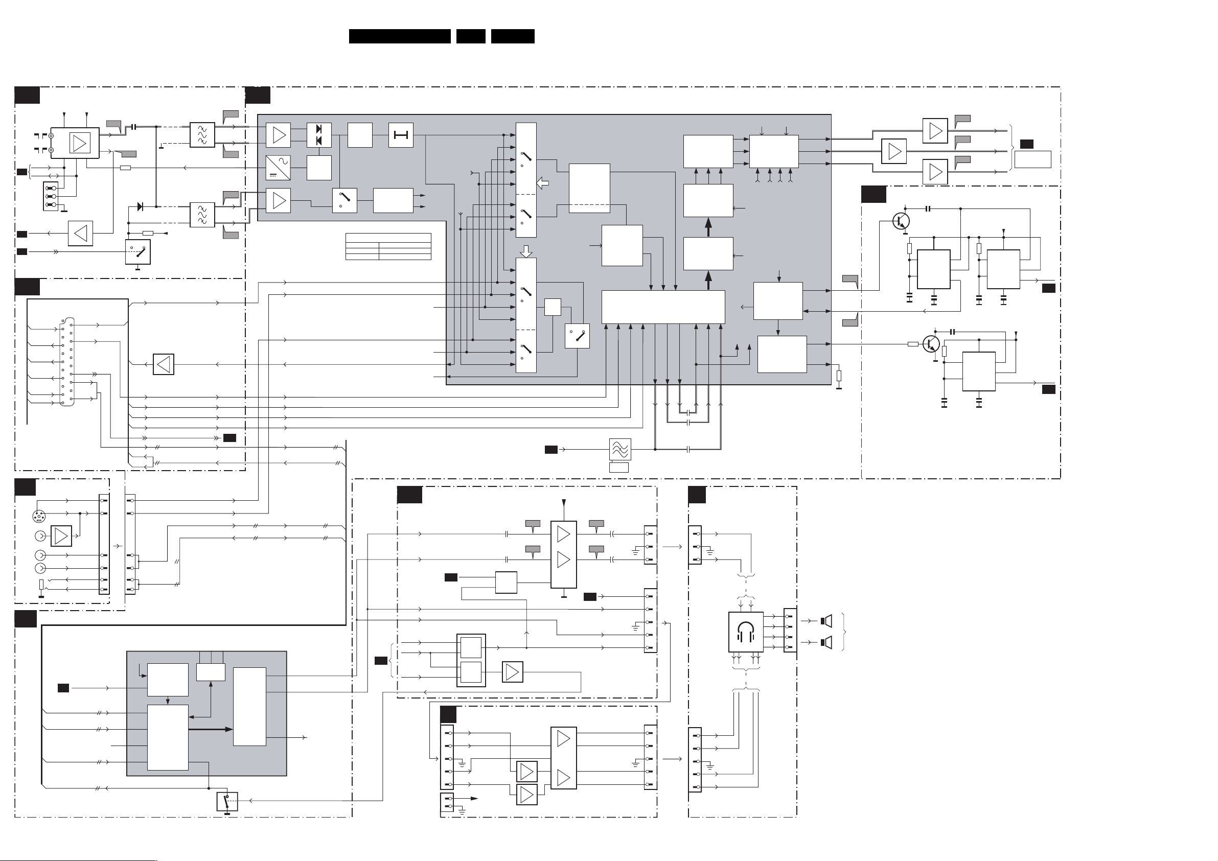
Block Diagram Audio & Video 16
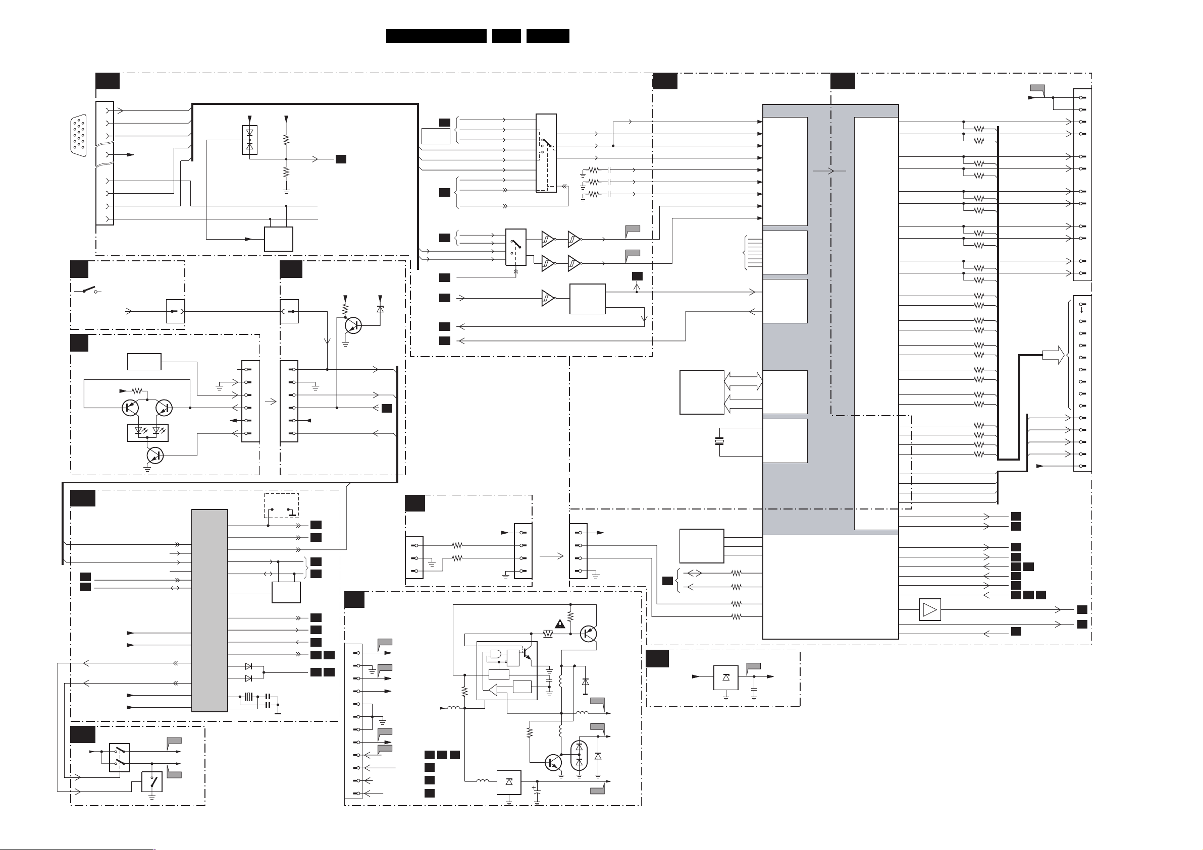
Block Diagram Scaler & Supply 17
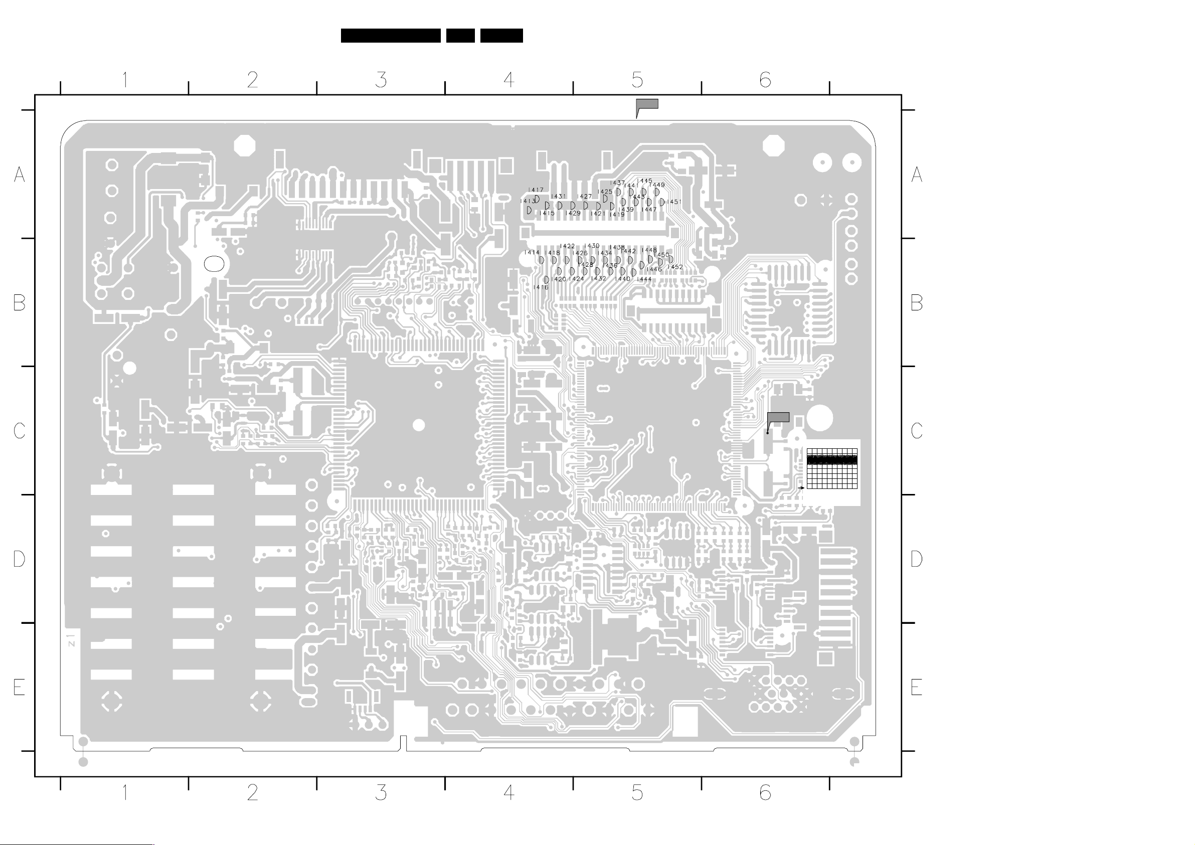
Testpoint Overview TV & Scaler Board 18-19
Testpoint Overview Front IR / LED Panel 20
I2C Overview 21
Supply Voltage Overview 22
7. Circuit Diagrams and PWB Layouts Diagram PWB
Tuner & VIF (Diagram A1) 23 32-33
Hercules (Diagram A2) 24 32-33
Hercules Supply (Diagram A3) 25 32-33
Audio Amplifier (2x2W) (Diagram A4) 26 32-33
TV-Supply (Diagram A5) 27 32-33
Scaler (Diagram A6) 28 32-33
Scaler LVDS (Diagram A7) 29 32-33
Scaler IO (Diagram A8) 30 32-33
Supply (Diagram A9) 31 32-33
Rear IO Scart (Diagram A10) 31 32-33
Side AV Panel (Diagram D) 34 35
Top Control Panel (Diagram E) 36 36
Audio Amplifier (2x5W) (20 & 23”)(Diagram I) 37 38
Front IR / LED Panel (Diagram J) 39 39
8. Alignments 41
9. Circuit Descriptions 45
Abbreviation List 49
IC Data Sheets 51
10 Spare Parts List 54
11 Revision List 57
©
Copyright 2004 Philips Consumer Electronics B.V. Eindhoven, The Netherlands.
All rights reserved. No part of this publication may be reproduced, stored in a
retrieval system or transmitted, in any form or by any means, electronic,
mechanical, photocopying, or otherwise without the prior permission of Philips.
Published by BB 0469 Service PaCE Printed in the Netherlands Subject to modification EN 3122 785 14520
EN 2 LC4.1E AA1.
Technical Specifications, Connections and Chassis Overview
1. Technical Specifications, Connections and Chassis Overview
1.1 Technical Specifications
1.1.1 Vision
Display type : 14 inch: LCD-VA
: 15 inch: DV-LCD-IPS
: 17-23 inch:
DV-LCD-IPS
Screen size: : 14 inch (37 cm)
: 15 inch (38 cm)
: 17 inch (45 cm)
: 20 inch (51 cm)
: 23 inch (59 cm)
Resolution (HxV) : 14 inch: 640x480
(VGA)
: 15 inch: 1024x768
(XGA)
: 17 inch: 1280x768
(WXGA)
: 20 inch: 640x480
(VGA)
: 23 inch: 1280x768
(WXGA)
Viewing angle : 14 inch: 170x170 deg.
: 15 inch: 130x100 deg.
: 17-23 inch:
176x176 deg.
Light output : 450 cd/m
Tuning system : PLL
Colour systems : PAL B/G, D/K, I
: SECAM B/G, D/K, L,
L1
Video playback : NTSC, PAL, SECAM
Channel selections : 100 channels
: PLL
Aerial input : 75 ohm
: Coax
1.1.2 Sound
Sound systems : BI NICAM BG
: 2CS BG
: FM/FM (5.5-5.74)
: (B/G)
: NICAM B/G (5.5-5.85)
: NICAM D/K (6.5-5.85)
: NICAM I (6.0-6.52)
: NICAM L (6.5(AM)-
5.85)
Maximum power : 14-17 inch: 2x2 W
: 20-23 inch: 2x5 W
1.1.3 Miscellaneous
Power supply:
- Mains voltage : 90-240 V ac
- Mains frequency : 50 / 60 Hz
Ambient conditions:
- Temperature range : +5 to +40 °C
- Maximum humidity : 90 % R.H.
1.2 Connections
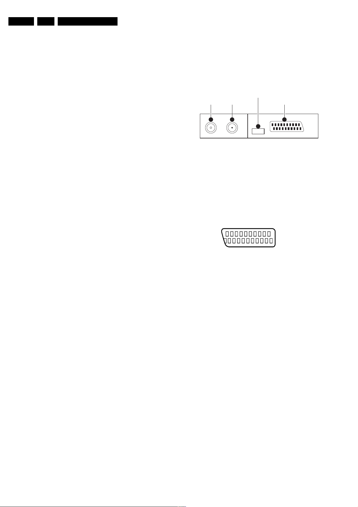
1.2.1 Rear Connections
ComPair
CONNECTOR
FM ANT SCART 1AERIAL IN
E_14520_050.eps
Figure 1-1 Rear connections
Aerial - In
- IEC-type Coax, 75 ohm D
FM Ant
- IEC-type Coax, 75 ohm D
SCART1: RGB/YUV - In, CVBS - In/Out, Audio - In/Out
2
1 - Audio - R 0.5 V_rms / 1 kohm k
2 - Audio - R 0.5 V_rms / 10 kohm j
3 - Audio - L 0.5 V_rms / 1 kohm k
4 - Audio - gnd Ground H
5 - Blue - gnd Ground H
6 - Audio - L 0.5 V_rms / 10 kohm j
7 - Blue/U - in 0.7 V_pp / 75 ohm j
8 - CVBS - status 0 - 2 V: INT
9 - Green - gnd Ground H
10 - n.c.
11 - Green/Y - in 0.7 V_pp / 75 ohm j
12 - n.c.
13 - Red - gnd Ground H
14 - FBL - gnd Ground H
15 - Red/V - in 0.7 V_pp / 75 ohm j
16 - Status/FBL 0 - 0.4 V: INT
17 - Video Ground H
18 - Video Ground H
19 - CVBS - out 1 V_pp / 75 ohm k
20 - CVBS - in 1 V_pp / 75 ohm j
21 - Shielding Ground H
20
21
Figure 1-2 SCART connector
4.5 - 7 V: EXT 16:9
9.5 - 12 V: EXT 4:3 j
1 - 3 V: EXT / 75 ohm j
2
E_06532_001.eps
1
050404
170904
Power consumption
- Normal operation : from 32 W
: to 110 W
- Standby : < 2 W
Technical Specifications, Connections and Chassis Overview
EN 3LC4.1E AA 1.
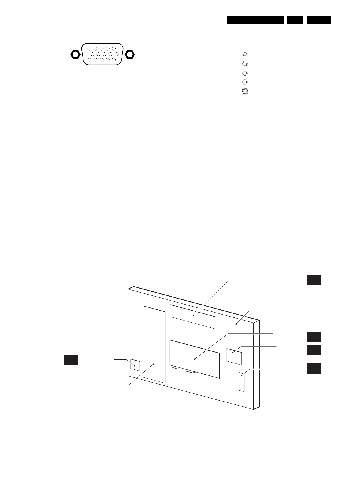
VGA: RGB - In
1
6
11
5
10
15
E_06532_002.eps
050404
Figure 1-3 VGA Connector
1 - Red 0.7 V_pp / 75 ohm j
2 - Green 0.7 V_pp / 75 ohm j
3 - Blue 0.7 V_pp / 75 ohm j
4 - Ground H
5 - Ground H
6 - Red - gnd Ground H
7 - Green - gnd Ground H
8 - Blue - gnd Ground H
9 - 5V_DC +5 V_dc j
10 - Ground H
11 - Ground H
12 - DDC_SDA DDC data j
13 - H-sync 0 - 5 V j
14 - V-sync 0 - 5 V j
15 - DDC_SCL DDC clock j
1.2.2 Side Connections
HEADPHONE
AUDIO R IN
AUDIO L IN
VIDEO IN
S-VIDEO
E_14520_051.eps
170904
Figure 1-4 Side connections
Mini Jack: Audio - in
4 - Audio - L 0.5 Vrms / 10 kohm jq
3 - Audio - R 0.5 Vrms / 10 kohm jq
S-VHS - In Hosiden
1 - Y Ground H
2 - C Ground H
3 - Y 1 Vpp/75 ohm j
4 - C 0.3 Vpp/75 ohm j
Video - In (Cinch)
1 - CVBS 1 Vpp/75 ohm jq
1.3 Chassis Overview
FRONT IR / LED
J
PANEL
Audio - In (Cinch)
1 - Audio - R 0.5 Vrms/10 k ohm jq
2 - Audio - L 0.5 Vrms/10 k ohm jq
Jack: Headphone- Out
Bk - Headphone 32 - 600 ohm / 10 mW rt
TOP CONTROL PANEL
LCD PANEL
TV & SCALER
BOARD
AMPLIFIER
PA NE L
SIDE IO PANEL
E
A
I
D
POWER SUPPLY
UNIT
E_14520_052.eps
200904
Figure 1-5 Chassis Overview

EN 4 LC4.1E AA2.
Safety Instructions, Warnings, and Notes
2. Safety Instructions, Warnings, and Notes
2.1 Safety Instructions
Safety regulations require that during a repair:
• Connect the set to the Mains (AC Power) via an isolation
transformer (> 800 VA).
• Replace safety components, indicated by the symbol h,
only by components identical to the original ones. Any
other component substitution (other than original type) may
increase risk of fire or electrical shock hazard.
Safety regulations require that after a repair, the set must be
returned in its original condition. Pay in particular attention to
the following points:
• Route the wire trees correctly and fix them with the
mounted cable clamps.
• Check the insulation of the Mains (AC Power) lead for
external damage.
• Check the strain relief of the Mains (AC Power) cord for
proper function.
• Check the electrical DC resistance between the Mains (AC
Power) plug and the secondary side (only for sets which
have a Mains (AC Power) isolated power supply):
1. Unplug the Mains (AC Power) cord and connect a wire
between the two pins of the Mains (AC Power) plug.
2. Set the Mains (AC Power) switch to the "on" position
(keep the Mains (AC Power) cord unplugged!).
3. Measure the resistance value between the pins of the
Mains (AC Power) plug and the metal shielding of the
tuner or the aerial connection on the set. The reading
should be between 4.5 Mohm and 12 Mohm.
4. Switch "off" the set, and remove the wire between the
two pins of the Mains (AC Power) plug.
• Check the cabinet for defects, to avoid touching of any
inner parts by the customer.
2.2 Warnings
• Where necessary, measure the waveforms and voltages
with (D) and without (E) aerial signal. Measure the
voltages in the power supply section both in normal
operation (G) and in standby (F). These values are
indicated by means of the appropriate symbols.
• The semiconductors indicated in the circuit diagram and in
the parts lists, are interchangeable per position with the
semiconductors in the unit, irrespective of the type
indication on these semiconductors.
• Manufactured under license from Dolby Laboratories.
“Dolby”, “Pro Logic” and the “double-D symbol”, are
trademarks of Dolby Laboratories.
E_06532_006.eps
240604
Figure 2-1 Dolby PL Symbol
2.3.2 Schematic Notes
• All resistor values are in ohms and the value multiplier is
often used to indicate the decimal point location (e.g. 2K2
indicates 2.2 kohm).
• Resistor values with no multiplier may be indicated with
either an "E" or an "R" (e.g. 220E or 220R indicates 220
ohm).
• All capacitor values are given in micro-farads (µ= x10
nano-farads (n= x10
• Capacitor values may also use the value multiplier as the
decimal point indication (e.g. 2p2 indicates 2.2 pF).
• An "asterisk" (*) indicates component usage varies. Refer
to the diversity tables for the correct values.
• The correct component values are listed in the Electrical
Replacement Parts List. Therefore, always check this list
when there is any doubt.
-9
), or pico-farads (p= x10
-12
-6
),
).
• All ICs and many other semiconductors are susceptible to
electrostatic discharges (ESD w). Careless handling
during repair can reduce life drastically. Make sure that,
during repair, you are connected with the same potential as
the mass of the set by a wristband with resistance. Keep
components and tools also at this same potential.
Available ESD protection equipment:
– Complete kit ESD3 (small tablemat, wristband,
connection box, extension cable and earth cable) 4822
310 10671.
– Wristband tester 4822 344 13999.
• Be careful during measurements in the high voltage
section.
• Never replace modules or other components while the unit
is switched "on".
• When you align the set, use plastic rather than metal tools.
This will prevent any short circuits and the danger of a
circuit becoming unstable.
2.3 Notes
2.3.1 General
• Measure the voltages and waveforms with regard to the
chassis (= tuner) ground (H), or hot ground (I), depending
on the tested area of circuitry. The voltages and waveforms
shown in the diagrams are indicative. Measure them in the
Service Default Mode (see chapter 5) with a colour bar
signal and stereo sound (L: 3 kHz, R: 1 kHz unless stated
otherwise) and picture carrier at 475.25 MHz for PAL, or
61.25 MHz for NTSC (channel 3).
2.3.3 Rework on BGA (Ball Grid Array) ICs
General
Although (LF)BGA assembly yields are very high, there may
still be a requirement for component rework. By rework, we
mean the process of removing the component from the PWB
and replacing it with a new component. If an (LF)BGA is
removed from a PWB, the solder balls of the component are
deformed drastically so the removed (LF)BGA has to be
discarded.
Device Removal
As is the case with any component that, it is essential when
removing an (LF)BGA, the board, tracks, solder lands, or
surrounding components are not damaged. To remove an
(LF)BGA, the board must be uniformly heated to a temperature
close to the reflow soldering temperature. A uniform
temperature reduces the chance of warping the PWB.
To do this, we recommend that the board is heated until it is
certain that all the joints are molten. Then carefully pull the
component off the board with a vacuum nozzle. For the
appropriate temperature profiles, see the IC data sheet.
Area Preparation
When the component has been removed, the vacant IC area
must be cleaned before replacing the (LF)BGA.
Removing an IC often leaves varying amounts of solder on the
mounting lands. This excessive solder can be removed with
either a solder sucker or solder wick. The remaining flux can be
removed with a brush and cleaning agent.
After the board is properly cleaned and inspected, apply flux on
the solder lands and on the connection balls of the (LF)BGA.

Safety Instructions, Warnings, and Notes
Note: Do not apply solder paste, as this has shown to result in
problems during re-soldering.
Device Replacement
The last step in the repair process is to solder the new
component on the board. Ideally, the (LF)BGA should be
aligned under a microscope or magnifying glass. If this is not
possible, try to align the (LF)BGA with any board markers.
To reflow the solder, apply a temperature profile according to
the IC data sheet. So as not to damage neighbouring
components, it may be necessary to reduce some
temperatures and times.
More Information
For more information on how to handle BGA devices, visit this
URL: www.atyourservice.ce.philips.com
not available for all regions) ). After login, select “Magazine”,
then go to “Workshop Information”. Here you will find
Information on how to deal with BGA-ICs.
2.3.4 Lead Free Solder
Some PWBs in this chassis are “lead-free prepared”. This is
indicated on the PWB by the PHILIPS lead-free logo (either by
a service-printing or by a sticker). It does not mean that leadfree solder is actually used!
(needs subscription,
EN 5LC4.1E AA 2.
P
b
Figure 2-2 Lead-free logo
Due to this fact, some rules have to be respected by the
workshop during a repair:
• Use only lead-free soldering tin Philips SAC305 with order
code 0622 149 00106. If lead-free solder paste is required,
please contact the manufacturer of your soldering
equipment.
• Use only adequate solder tools applicable for lead-free
soldering tin.
• Adjust your solder tool so that a temperature around 217 220 deg. C is reached at the solder joint.
• Do not mix lead-free soldering tin with leaded soldering tin;
this will lead to unreliable solder joints!
• Use only original spare parts listed in this manual. These
are lead-free parts!
• On the website www.atyourservice.ce.philips.com
subscription, not available for all regions) you can find
more information on:
– Aspects of lead-free technology.
– BGA (de-)soldering, heating-profiles of BGAs used in
Philips sets, and others.
2.3.5 Practical Service Precautions
(needs
• It makes sense to avoid exposure to electrical shock.
While some sources are expected to have a possible
dangerous impact, others of quite high potential are of
limited current and are sometimes held in less regard.
• Always respect voltages. While some may not be
dangerous in themselves, they can cause unexpected
reactions - reactions that are best avoided. Before reaching
into a powered TV set, it is best to test the high voltage
insulation. It is easy to do, and is a good service precaution.

EN 6 LC4.1E AA3.
3. Directions for Use
You can download this information from the following website:
http://www.philips.com/support
Directions for Use
4. Mechanical Instructions
Mechanical Instructions
EN 7LC4.1E AA 4.
Index of this chapter:
1. Service Position
2. Rear Cover Removal
3. Power Supply Unit Removal
4. TV & Scaler Board Removal
5. Side I/O Panel Removal
6. Top Control Panel Removal
7. Audio Amplifier Panel Removal
8. Exchanging the LCD Panel
9. Re-assembly
Note: Figures below can deviate from the actual situation, due
to different set executions.
Note: To diagnose the set with ComPair it is not needed to
open the set entirely.
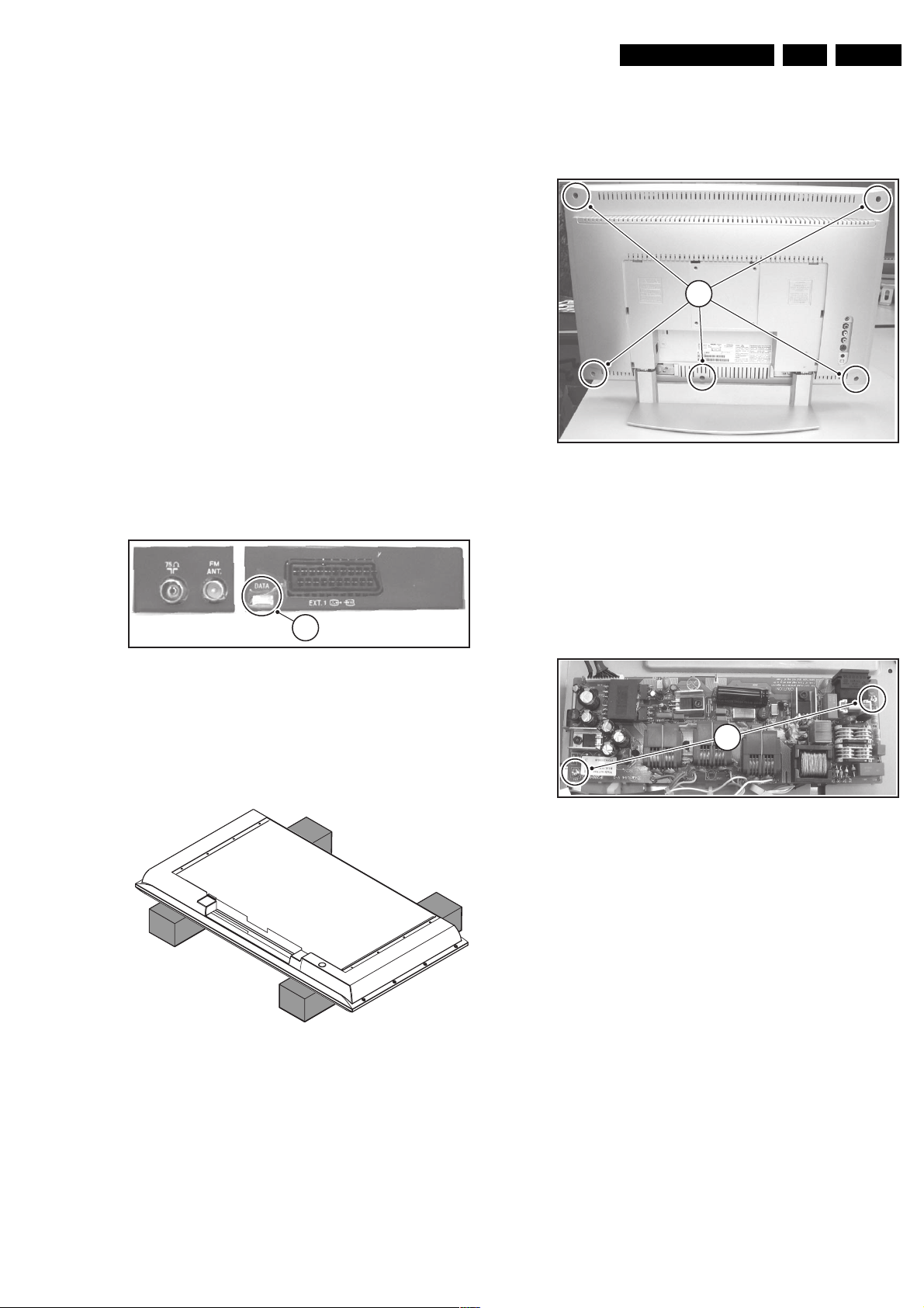
To access the ComPair connector, proceed with the following:
1. Manually unlock and remove the cover cap.
2. Remove the tape shielding that covers the ComPair
connector (1).
Note: Make sure that both the ComPair connector and the
UART connector are shielded off with a piece of insulating tape
after repair for ESD reasons. Place this tape over the holes in
the rear cover of the set.
4.2 Rear Cover Removal
1
Figure 4-3 Rear cover removal
1. Make sure all power-, audio-, video- and coax- cables are
unplugged.
2. Remove all Torx screws (1) around the edges of the rear
cover.
3. Remove the rear cover and store it in a safe place.
E_14520_035.eps
160904
Figure 4-1 ComPair connector
4.1 Service Position
4.1.1 Foam Bars
Figure 4-2 Foam bars
1
E_14520_034.eps
160904
E_06532_018.eps
170504
4.3 Power Supply Unit Removal
1
Figure 4-4 Power supply unit
1. Disconnect all cables from the Power supply unit.
2. Remove all mounting screws (1) from the Power supply
unit.
3. Take out the Power supply unit.
E_14520_036.eps
160904
The foam bars (order code 3122 785 90580) can be used for
all types and sizes of Flat TVs. By laying the plasma or LCD TV
flat on the (ESD protective) foam bars, a stable situation is
created to perform measurements and alignments. By placing
a mirror under the TV, you can easily monitor the screen.
EN 8 LC4.1E AA4.
Mechanical Instructions
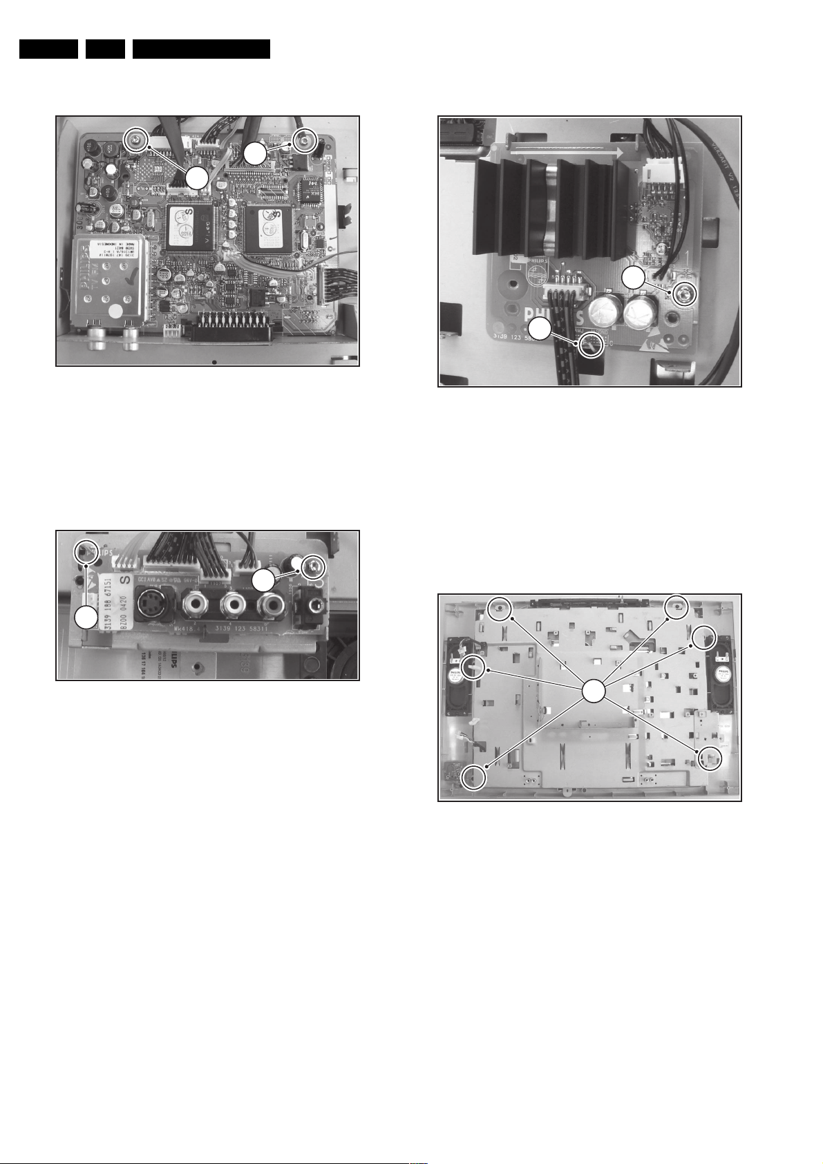
4.4 TV & Scaler Board Removal
1
2
Figure 4-5 TV & Scaler board removal
1. Disconnect all cables from the TV & Scaler board.
2. Remove the screw from the grounding cable (1).
3. Remove the mounting screw (2) and remove the board.
4.5 Side I/O Panel Removal
E_14520_037.eps
160904
4.7 Audio Amplifier Panel Removal
1
2
Figure 4-7 Audio amplifier panel removal
1. Disconnect all cables from the audio amplifier panel.
2. Remove all mounting screws from the audio amplifier panel
(1).
3. Unlock the panel by twisting back the clamp at the bottom
(2).
4. Take out the audio amplifier panel.
E_14520_039.eps
160904
1
2
Figure 4-6 Side I/O panel removal
1. Disconnect all cables from the Side I/O panel.
2. Remove the mounting screw (1).
3. Unlock the panel by twisting back the clamp at the bottom
(2).
4. Take out the Side I/O panel from the bracket.
4.6 Top Control Panel Removal
1. Disconnect the cable from the top control panel.
2. Remove the two mounting screws from the top control
panel.
3. Take out the top control panel.
E_14520_038.eps
160904
4.8 Exchanging the LCD Panel
1
Figure 4-8 Exchanging the LCD panel
1. Disconnect all cables from the LCD Panel.
2. Remove all mounting screws (1) from the metal cover.
3. Lift and take off the metal cover.
4. Now you can exchange the LCD panel.
4.9 Re-Assembly
E_14520_040.eps
160904
To re-assemble the whole set, do all processes in reverse
order.
Notes:
Do not forget to replace the ground cable of the TV & Scaler
board, while mounting the screw at the board topside. See
figure “TV & Scaler board removal”.
Service Modes, Error Codes, and Fault Finding
5. Service Modes, Error Codes, and Fault Finding
EN 9LC4.1E AA 5.
Index of this chapter:
1. Test Points
2. Service Modes
3. Problems and Solving Tips (related to CSM)
4. ComPair
5. Error Codes
6. The Blinking LED Procedure
7. Fault Finding and Repair Tips
5.1 Test Points
This chassis is equipped with test points in the service printing.
In the schematics test points are identified with a rectangle box
around Fxxx or Ixxx. These test points are specifically
mentioned in the service manual as “half moons” with a dot in
the centre.
Perform measurements under the following conditions:
• Television set in Service Default Alignment Mode.
• Video input: Colour bar signal.
• Audio input: 3 kHz left channel, 1 kHz right channel.
5.2 Service Modes
Service Default mode (SDM) and Service Alignment Mode
(SAM) offers several features for the service technician, while
the Customer Service Mode (CSM) is used for communication
between the call centre and the customer.
This chassis also offers the option of using ComPair, a
hardware interface between a computer and the TV chassis. It
offers the abilities of structured troubleshooting, error code
reading, and software version readout for all chassis.
Minimum requirements for ComPair: a Pentium processor, a
Windows OS, and a CD-ROM drive (see also paragraph
"ComPair").
5.2.1 Service Default Mode (SDM)
Purpose
• To create a predefined setting for measurements to be
made.
• To override software protections.
• To start the blinking LED procedure.
• To inspect the error buffer.
• To check the life timer.
How to enter
To enter SDM, use one of the following methods:
• Press the following key sequence on the remote control
transmitter: “062596” directly followed by the MENU button
(do not allow the display to time out between entries while
keying the sequence).
• Short "Service" jumpers on the TV board during cold start
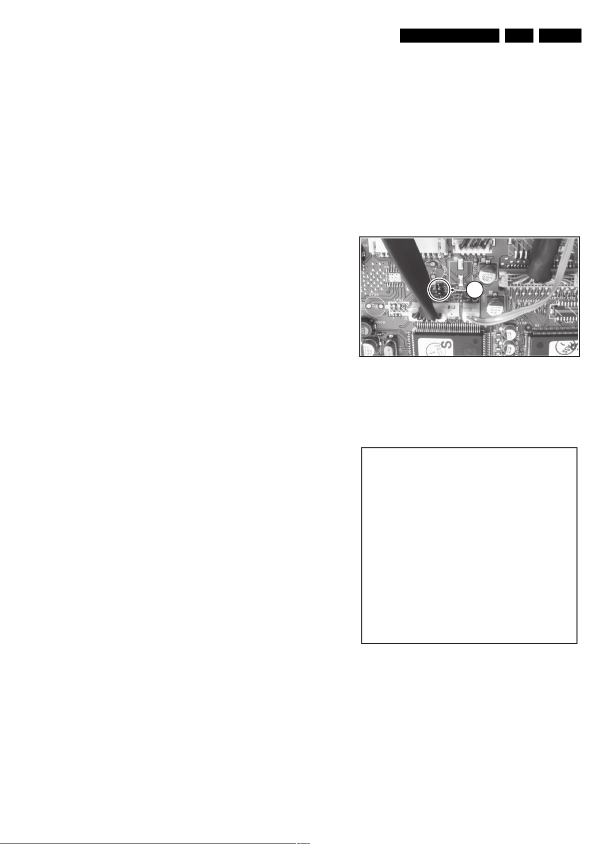
and apply mains (see Figure "Service jumpers"). Then
press the mains button (remove the short after start-up).
Caution: Entering SDM by shorting "Service" jumpers will
override the +5V-protection. Do this only for a short period.
When doing this, the service-technician must know exactly
what he is doing, as it could damage the television set.
• Or via ComPair.
1
E_14520_041.eps
160904
Figure 5-1 Service jumpers
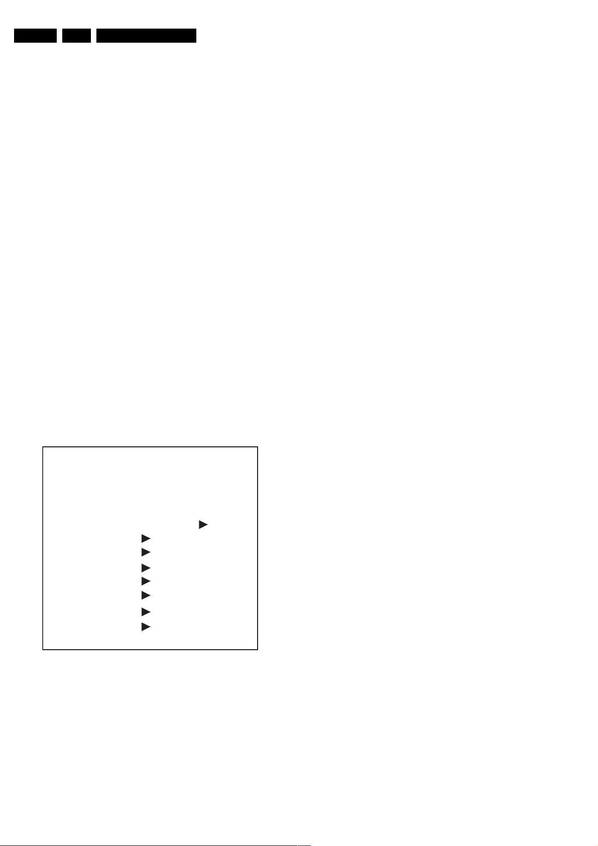
After entering SDM, the following screen is visible, with SDM in
the upper right corner of the screen to indicate that the
television is in Service Default Alignment Mode.
00022 LC41EP1 1.00/S41EV1 1.01 SDM
ERR 0 0 0 0 0
OP 000 057 140 032 120 128 000
Specifications
• Tuning frequency: 475.25 MHz.
• Colour system: PAL-BG.
• All picture settings at 50% (brightness, colour contrast,
hue).
• Bass, treble and balance at 50 %; volume at 25 %.
• All service-unfriendly modes (if present) are disabled. The
service unfriendly modes are:
– Timer / Sleep timer.
– Child / parental lock.
– Blue mute.
– Hotel / hospital mode.
– Auto shut off (when no “IDENT” video signal is
received for 15 minutes).
– Skipping of non-favourite presets / channels.
– Auto-storage of personal presets.
– Auto user menu time-out.
– Auto Volume Levelling (AVL).
E_14520_042.eps
160904
Figure 5-2 SDM menu
How to navigate
Use one of the following methods:
• When you press the MENU button on the remote control,
the set will switch on the normal user menu in the SDM
mode.
• On the TV, press and hold the VOLUME DOWN and press
the CHANNEL DOWN for a few seconds, to switch from
SDM to SAM and reverse.
EN 10 LC4.1E AA5.
Service Modes, Error Codes, and Fault Finding
How to exit
Switch the set to STANDBY by pressing the mains button on
the remote control transmitter or the television set.
If you turn the television set off by removing the mains (i.e.,
unplugging the television) without using the mains button, the
television set will remain in SDM when mains is re-applied, and
the error buffer is not cleared.
5.2.2 Service Alignment Mode (SAM)
Purpose
• To change option settings.
• To display / clear the error code buffer.
• To perform alignments.
Specifications
• Operation hours counter (maximum five digits displayed).
• Software version, Error codes, and Option settings display.
• Error buffer clearing.
• Option settings.
• AKB switching.
• Software alignments (Tuner, White Tone, Geometry &
Audio).
• NVM Editor.
• ComPair Mode switching.
How to enter
To enter SAM, use one of the following methods:
• Press the following key sequence on the remote control
transmitter: “062596" directly followed by the OSD/
STATUS button (do not allow the display to time out
between entries while keying the sequence).
• Or via ComPair.
After entering SAM, the following screen is visible, with SAM in
the upper right corner of the screen to indicate that the
television is in Service Alignment Mode.
00022 LC41EP1 1.00/S41EV1 1.01 SAM
ERR 0 0 0 0 0
• Europe: T= 1 page TXT, F= Full TXT, V= Voice
control.
• LATAM and NAFTA: N= Stereo non-dBx, S=
Stereo dBx.
• Asian Pacific: T= TXT, N= non-TXT, C= NTSC.
• ALL regions: M= mono, D= DVD, Q= Mk2.
– D= the language cluster number.
– X= the main software version number (updated with a
major change that is incompatible with previous
versions).
– Y= the sub software version number (updated with a
minor change that is compatible with previous
versions).
– EEEEEE= the scaler sw cluster
– F= the main sw version no.
– GG= the sub-version no.
3. SAM. Indication of the Service Alignment Mode.
4. Error Buffer. Shows all errors detected since the last time
the buffer was erased. Five errors possible.
5. Option Bytes. Used to set the option bytes. See “Options”
in the Alignments section for a detailed description. Seven
codes are possible.
6. Clear. Erases the contents of the error buffer. Select the
CLEAR menu item and press the MENU RIGHT key. The
content of the error buffer is cleared.
7. Options. Used to set the option bits. See “Options” in the
Alignments section for a detailed description.
8. Tuner. Used to align the tuner. See “Tuner” in the
Alignments section for a detailed description.
9. White Tone. Used to align the white tone. See “White
Tone” in the Alignments section for a detailed description.
10. Audio. No audio alignment is necessary for this television
set.
11. NVM Editor. Can be used to change the NVM data in the
television set. See table “NVM data” further on.
12. SC NVM Editor. Can be used to edit Scaler NVM.
13. ComPaIr. Can be used to switch on the television to In
System Programming (ISP) mode, for software uploading
via ComPair.
Caution: When this mode is selected without ComPair
connected, the TV will be blocked. Remove the AC power
to reset the TV.
OP 000 057 140 032 120 128 000
. Clear Clear ?
. Options
. Tuner
. White Tone
. Audio
. NVM Editor
. SC NVM Editor
. ComPair Mode On
E_14520_043.eps
160904
Figure 5-3 SAM menu
Menu explanation
1. LLLLL. This represents the run timer. The run timer counts
normal operation hours, but does not count standby hours.
2. AAABCD-X.Y. This is the software identification of the
main microprocessor:
– A= the project name (LC41).
– B= the region: E= Europe, A= Asia Pacific, U= NAFTA,
L= LATAM.
– C= the software diversity:
How to navigate
• In SAM, select menu items with the MENU UP/DOWN keys
on the remote control transmitter. The selected item will be
highlighted. When not all menu items fit on the screen, use
the MENU UP/DOWN keys to display the next / previous
menu items.
• With the MENU LEFT/RIGHT keys, it is possible to:
– Activate the selected menu item.
– Change the value of the selected menu item.
– Activate the selected submenu.
• In SAM, when you press the MENU button twice, the set
will switch to the normal user menus (with the SAM mode
still active in the background). To return to the SAM menu
press the MENU or STATUS/EXIT button.
• When you press the MENU key in while in a submenu, you
will return to the previous menu.
How to store SAM settings
To store the settings changed in SAM mode, leave the top level
SAM menu by using the POWER button on the remote control
transmitter or the television set.
How to exit
Switch the set to STANDBY by pressing the mains button on
the remote control transmitter or the television set.
If you turn the television set “off” by removing the mains (i.e.,
unplugging the television) without using the mains button, the
television set will remain in SAM when mains is re-applied, and
the error buffer is not cleared.

Service Modes, Error Codes, and Fault Finding
EN 11LC4.1E AA 5.
5.2.3 Customer Service Mode (CSM)
Purpose
The Customer Service Mode shows error codes and
information on the TV’s operation settings. The call centre can
instruct the customer (by telephone) to enter CSM in order to
identify the status of the set. This helps the call centre to
diagnose problems and failures in the TV set before making a
service call.
The CSM is a read-only mode; therefore, modifications are not
possible in this mode.
How to enter
To enter CSM, press the following key sequence on the remote
control transmitter: “123654” (do not allow the display to time
out between entries while keying the sequence).
Upon entering the Customer Service Mode, the following
screen will appear:
1 00022 LC41EP1 1.00/S41EV1 1.01 CSM
2 CODES 0 0 0 0 0
3 OP 000 057 140 032 120 128 000
4 20PF8846/12
5
6 NOT TUNED
7 PAL
8 STEREO
9 CO 50 CL 50 BR 50
0 AVL Off
5.3 Problems and Solving Tips Related to CSM
5.3.1 Picture Problems
Note: The problems described below are all related to the TV
settings. The procedures used to change the value (or status)
of the different settings are described.
Picture too dark or too bright
If:
• The picture improves when you press the AUTO PICTURE
button on the remote control transmitter, or
• The picture improves when you enter the Customer
Service Mode,
Then:
1. Press the AUTO PICTURE button on the remote control
transmitter repeatedly (if necessary) to choose
PERSONAL picture mode.
2. Press the MENU button on the remote control transmitter.
This brings up the normal user menu.
3. In the normal user menu, use the MENU UP/DOWN keys
to highlight the PICTURE sub menu.
4. Press the MENU LEFT/RIGHT keys to enter the PICTURE
sub menu.
5. Use the MENU UP/DOWN keys (if necessary) to select
BRIGHTNESS.
6. Press the MENU LEFT/RIGHT keys to increase or
decrease the BRIGHTNESS value.
7. Use the MENU UP/DOWN keys to select PICTURE.
8. Press the MENU LEFT/RIGHT keys to increase or
decrease the PICTURE value.
9. Press the MENU button on the remote control transmitter
twice to exit the user menu.
10. The new PERSONAL preference values are automatically
stored.
E_14520_044.eps
160904
Figure 5-4 CSM menu
Menu explanation
1. Indication of the decimal value of the operation hours
counter, Software identification of the main microprocessor
(see "Service Default or Alignment Mode" for an
explanation), and the service mode (CSM= Customer
Service Mode).
2. Displays the last five errors detected in the error code
buffer.
3. Displays the option bytes.
4. Displays the type number version of the set.
5. Reserved item for P3C call centres (AKBS stands for
Advanced Knowledge Base System).
6. Indicates the television is receiving an "IDENT" signal on
the selected source. If no "IDENT" signal is detected, the
display will read "NOT TUNED"
7. Displays the detected Colour system (e.g. PAL/NTSC).
8. Displays the detected Audio (e.g. stereo/mono).
9. Displays the picture setting information.
10. Displays the sound setting information.
How to exit
To exit CSM, use one of the following methods:
• Press the MENU, STATUS/EXIT, or POWER button on the
remote control transmitter.
• Press the POWER button on the television set.
White line around picture elements and text
If:
The picture improves after you have pressed the AUTO
PICTURE button on the remote control transmitter,
Then:
1. Press the AUTO PICTURE button on the remote control
transmitter repeatedly (if necessary) to choose
PERSONAL picture mode.
2. Press the MENU button on the remote control transmitter.
This brings up the normal user menu.
3. In the normal user menu, use the MENU UP/DOWN keys
to highlight the PICTURE sub menu.
4. Press the MENU LEFT/RIGHT keys to enter the PICTURE
sub menu.
5. Use the MENU UP/DOWN keys to select SHARPNESS.
6. Press the MENU LEFT key to decrease the SHARPNESS
value.
7. Press the MENU button on the remote control transmitter
twice to exit the user menu.
8. The new PERSONAL preference value is automatically
stored.
Snowy picture
Check CSM line 6. If this line reads “Not Tuned”, check the
following:
• Antenna not connected. Connect the antenna.
• No antenna signal or bad antenna signal. Connect a proper
antenna signal.
• The tuner is faulty (in this case line 2, the Error Buffer line,
will contain error number 10). Check the tuner and replace/
repair the tuner if necessary.

EN 12 LC4.1E AA5.
Service Modes, Error Codes, and Fault Finding
Black and white picture
If:
• The picture improves after you have pressed the AUTO
PICTURE button on the remote control transmitter,
Then:
1. Press the AUTO PICTURE button on the remote control
transmitter repeatedly (if necessary) to choose
PERSONAL picture mode.
2. Press the MENU button on the remote control transmitter.
This brings up the normal user menu.
3. In the normal user menu, use the MENU UP/DOWN keys
to highlight the PICTURE sub menu.
4. Press the MENU LEFT/RIGHT keys to enter the PICTURE
sub menu.
5. Use the MENU UP/DOWN keys to select COLOUR.
6. Press the MENU RIGHT key to increase the COLOUR
value.
7. Press the MENU button on the remote control transmitter
twice to exit the user menu.
8. The new PERSONAL preference value is automatically
stored.
Menu text not sharp enough
If:
• The picture improves after you have pressed the AUTO
PICTURE button on the remote control transmitter,
Then:
1. Press the AUTO PICTURE button on the remote control
transmitter repeatedly (if necessary) to choose
PERSONAL picture mode.
2. Press the MENU button on the remote control transmitter.
This brings up the normal user menu.
3. In the normal user menu, use the MENU UP/DOWN keys
to highlight the PICTURE sub menu.
4. Press the MENU LEFT/RIGHT keys to enter the PICTURE
sub menu.
5. Use the MENU UP/DOWN keys to select PICTURE.
6. Press the MENU LEFT key to decrease the PICTURE
value.
7. Press the MENU button on the remote control transmitter
twice to exit the user menu.
8. The new PERSONAL preference value is automatically
stored.
5.4 ComPair
Note: Make sure that both the ComPair connector and the
UART connector are shielded off with a piece of insulating tape
after repair for ESD reasons. Place this tape over the holes in
the rear cover of the set.
5.4.1 Introduction
the Force/SearchMan electronic manual of the defective
chassis, schematics and PWBs are only a mouse click
away.
5.4.2 Specifications
ComPair consists of a Windows based fault finding program
and an interface box between PC and the (defective) product.
The ComPair interface box is connected to the PC via a serial
(or RS232) cable.
For this chassis, the ComPair interface box and the TV
communicate via a bi-directional service cable via the service
connector(s).
The ComPair fault finding program is able to determine the
problem of the defective television. ComPair can gather
diagnostic information in two ways:
• Automatic (by communication with the television): ComPair
can automatically read out the contents of the entire error
buffer. Diagnosis is done on I
access the I
send and receive I
2
C/UART bus of the television. ComPair can
2
C/UART commands to the micro
2
C/UART level. ComPair can
controller of the television. In this way, it is possible for
ComPair to communicate (read and write) to devices on
2
the I
C/UART buses of the TV-set.
• Manually (by asking questions to you): Automatic
diagnosis is only possible if the micro controller of the
television is working correctly and only to a certain extend.
When this is not the case, ComPair will guide you through
the fault finding tree by asking you questions (e.g. Does the
screen give a picture? Click on the correct answer: YES /
NO) and showing you examples (e.g. Measure test-point I7
and click on the correct oscillogram you see on the
oscilloscope). You can answer by clicking on a link (e.g.
text or a waveform picture) that will bring you to the next
step in the fault finding process.
By a combination of automatic diagnostics and an interactive
question / answer procedure, ComPair will enable you to find
most problems in a fast and effective way.
Beside fault finding, ComPair provides some additional
features like:
• Up- or downloading of pre-sets.
• Managing of pre-set lists.
• Emulation of the (European) Dealer Service Tool (DST).
• If both ComPair and Force/SearchMan (Electronic Service
Manual) are installed, all the schematics and the PWBs of
the set are available by clicking on the appropriate
hyperlink.
Example: Measure the DC-voltage on capacitor C2568
(Schematic/Panel) at the Mono-carrier.
– Click on the “Panel” hyperlink to automatically show
the PWB with a highlighted capacitor C2568.
– Click on the “Schematic” hyperlink to automatically
show the position of the highlighted capacitor.
5.4.3 How To Connect
ComPair (Computer Aided Repair) is a service tool for Philips
Consumer Electronics products. ComPair is a further
development on the European DST (service remote control),
which allows faster and more accurate diagnostics. ComPair
has three big advantages:
• ComPair helps you to quickly get an understanding on how
to repair the chassis in a short time by guiding you
systematically through the repair procedures.
• ComPair allows very detailed diagnostics (on I
is therefore capable of accurately indicating problem areas.
You do not have to know anything about I
2
C level) and
2
C commands
yourself because ComPair takes care of this.
• ComPair speeds up the repair time since it can
automatically communicate with the chassis (when the
microprocessor is working) and all repair information is
directly available. When ComPair is installed together with
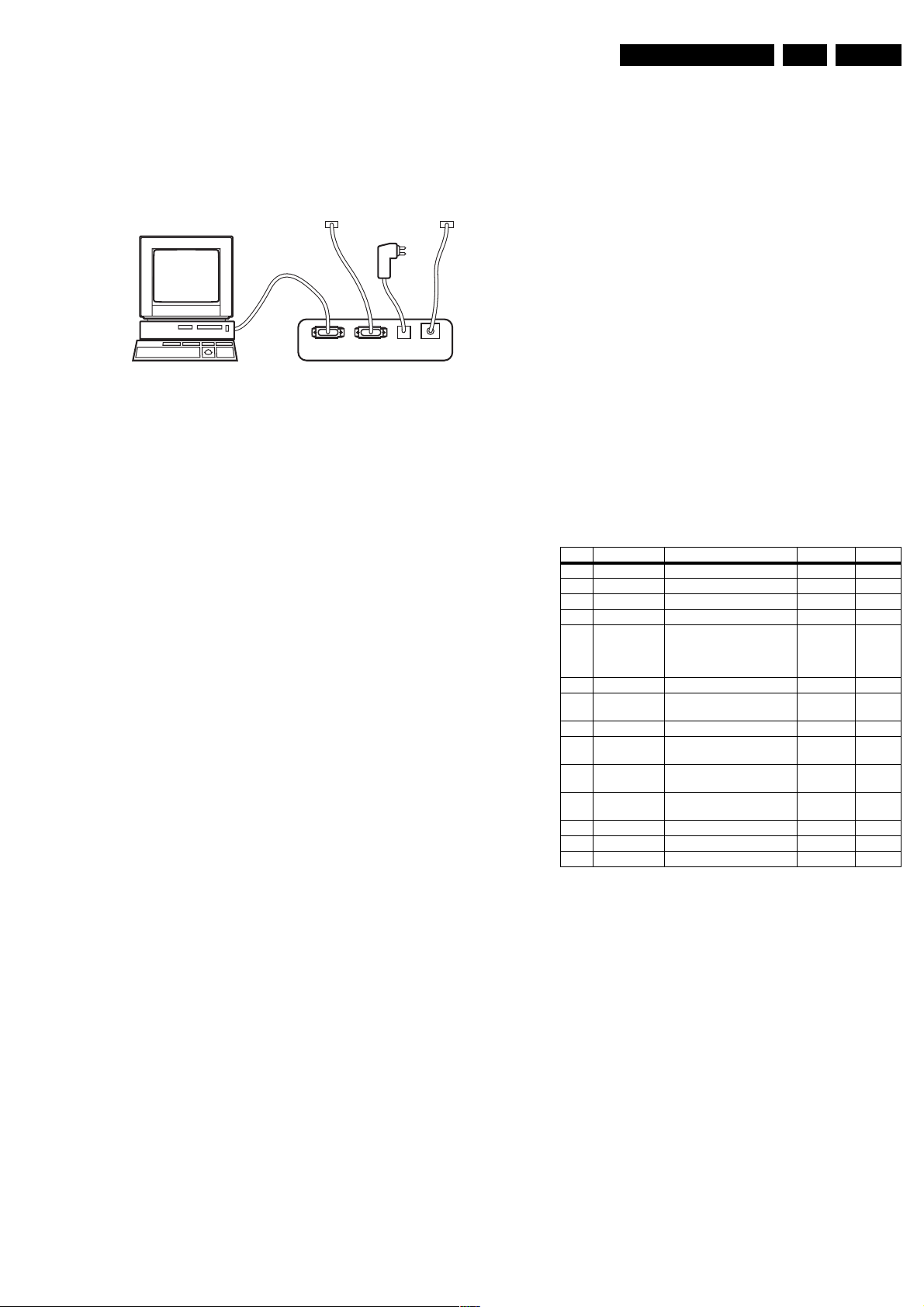
1. First, install the ComPair Browser software (see the Quick
Reference Card for installation instructions).
2. Connect the RS232 interface cable between a free serial
(COM) port of your PC and the PC connector (marked with
“PC”) of the ComPair interface.
3. Connect the mains adapter to the supply connector
(marked with “POWER 9V DC”) of the ComPair interface.
4. Switch the ComPair interface “OFF”.
5. Switch the television set “OFF” with the POWER switch.
6. Connect the ComPair I
the connector on the rear side of the ComPair interface
(marked with “I
“VCR”) and the appropriate ComPair connector at the rear
side of the TV (I
Note: Some chassis need an additional I
2
C/UART interface cable between
2
C” or for UART on the connector marked
2
C or UART).
2
C extension
cable due to a different connector pitch!
Service Modes, Error Codes, and Fault Finding
EN 13LC4.1E AA 5.
7. Plug the mains adapter in a mains outlet, and switch the
interface “ON”. The green and red LEDs light up together.
The red LED extinguishes after approx. 1 second while the
green LED remains lit.
8. Start the ComPair program and read the “Introduction”
chapter.
TO
UART SERVICE
CONNECTOR
PC VCR I2CPower
Figure 5-5 ComPair Interface connection
5.4.4 How To Order
ComPair order codes (EU/AP/LATAM):
• Starter kit ComPair32/SearchMan32 software and
ComPair interface (excl. transformer): 3122 785 90450.
• ComPair interface (excluding transformer): 4822 727
21631.
• Starter kit ComPair32 software (registration version): 3122
785 60040.
• Starter kit SearchMan32 software: 3122 785 60050.
• ComPair32 CD (update): 3122 785 60070 (year 2002,
3122 785 60110 (year 2003).
• SearchMan32 CD (update): 3122 785 60080 (year 2002),
3122 785 60120 (year 2003), 3122 785 60130 (year 2004).
• ComPair I
2
C interface cable: 3122 785 90004.
• ComPair firmware upgrade IC: 3122 785 90510.
• Transformer (non-UK): 4822 727 21632.
• Transformer (UK): 4822 727 21633.
• ComPair I
2
C extension cable: 3139 131 03791.
• ComPair UART interface cable: 3122 785 90630.
Note: If you encounter any problems, contact your local
support desk.
5.5 Error Codes
The error code buffer contains all errors detected since the last
time the buffer was erased. The buffer is written from left to
right. When an error occurs that is not yet in the error code
buffer, it is displayed at the left side and all other errors shift one
position to the right.
5.5.1 How To Read The Error Buffer
You can read the error buffer in 3 ways:
• On screen via the SAM (if you have a picture).
Examples:
– ERROR: 0 0 0 0 0 : No errors detected
– ERROR: 6 0 0 0 0 : Error code 6 is the last and only
detected error
– ERROR: 9 6 0 0 0 : Error code 6 was detected first and
error code 9 is the last detected (newest) error
• Via the blinking LED procedure (when you have no
picture). See “The Blinking LED Procedure”.
• Via ComPair.
5.5.2 How To Clear The Error Buffer
The error code buffer is cleared in the following cases:
• By using the CLEAR command in the SAM menu:
TO
I2C SERVICE
CONNECTOR
9V DC
E_06532_021.eps
180804
– To enter SAM, press the following key sequence on the
remote control transmitter: “062596” directly followed
by the OSD/STATUS button (do not allow the display
to time out between entries while keying the
sequence).
– Make sure the menu item CLEAR is highlighted. Use
the MENU UP/DOWN buttons, if necessary.
– Press the MENU RIGHT button to clear the error
buffer. The text on the right side of the “CLEAR” line will
change from “CLEAR?” to “CLEARED”
• If the contents of the error buffer have not changed for 50
hours, the error buffer resets automatically.
Note: If you exit SAM by disconnecting the mains from the
television set, the error buffer is not reset.
5.5.3 Error Codes
In case of non-intermittent faults, write down the errors present
in the error buffer and clear the error buffer before you begin
the repair. This ensures that old error codes are no longer
present.
If possible, check the entire contents of the error buffer. In
some situations, an error code is only the result of another error
and not the actual cause of the problem (for example, a fault in
the protection detection circuitry can also lead to a protection).
Table 5-1 Error code overview
Error Device Error description Check item Diagram
0 Not applicable No Error
1 Not applicable - - -
2 Not applicable - - -
3 Not applicable - - -
4 GM5221 I2C error while communicating
5 Not applicable +5v protection 7930 A6
6 I2C bus General I2C error 7011, 3083,
7 Not applicable - - -
8 M24C32 I2C error while communicating
9 M24C16 I2C error while communicating
10 Tuner I2C error while communicating
11 Not applicable - - -
12 Not applicable - - -
13 Not applicable - - -
with the Genesis Scaler
and/or Flash-ROM is faulty/
empty
with the Scaler EEPROM
with the EEPROM
with the PLL tuner
7401
7403
3084
7402 A7
7099 A2
1302, 3302,
3303, 3327
5.6 The Blinking LED Procedure
Using this procedure, you can make the contents of the error
buffer visible via the front LED. This is especially useful when
there is no picture.
When the SDM is entered, the front LED will blink the contents
of the error-buffer:
• The Led blinks with as many pulses as the error code
number, followed by a time period of 1.5 seconds, in which
the Led is off.
• Then this sequence starts is repeated.
Any RC5 command terminates this sequence.
Example of error buffer: 12 9 6 0 0
After entering SDM, the following occurs:
• 1 long blink of 5 seconds to start the sequence,
• 12 short blinks followed by a pause of 1.5 seconds,
• 9 short blinks followed by a pause of 1.5 seconds,
• 6 short blinks followed by a pause of 1.5 seconds,
• 1 long blink of 1.5 seconds to finish the sequence,
• The sequence starts again at 12 short blinks.
A6
A2
A1

EN 14 LC4.1E AA5.
Service Modes, Error Codes, and Fault Finding
5.7 Fault Finding and Repair Tips
Notes:
• It is assumed that the components are mounted correctly
with correct values and no bad solder joints.
• Before any fault finding actions, check if the correct options
are set.
5.7.1 NVM Editor
In some cases, it can be handy if one directly can change the
NVM contents. This can be done with the “NVM Editor” in SAM
mode.
5.7.2 Tuner and IF
No Picture in RF mode
1. Check whether picture is present in AV. If not, go to Video
processing troubleshooting section.
2. If present, check that the Option settings are correct.
3. Check that all supply voltages are present.
4. Check if I2C lines are working correctly (3.3V).
5. Manually store a known channel and check if there is IF
output at Tuner pin 11.
6. Feed in 105 dBuV at Tuner pin 11 and check whether there
is RGB output from Video Processing IC. If yes, Tuner may
be defected. Change Tuner.
Sound in picture problem for L' system (rolling horizontal lines)
1. Check whether AGC L' in Sam mode is set to 0.
2. If yes, align the set to correct value.
Required system is not selected correctly
1. Check whether the Service jumper (#4022, 08 05 size) is
present. If yes, remove it.
2. Check whether SEL_IF pin is according to what is
specified.
5.7.4 Power Supply
Check fuses
This power supply contains three fuses. One is near the mains
inlet (marked on the board as 1102) and two other are near the
output connectors (marked 1610 and 1660).
1. Check with power supply in off state by means of ohmic
measurement.
2. Fuse 1102 may open in case of severe lightning strikes
and/or failures in the power supply. Despite the fact, that
this fuse is mounted in a fuse holder and the marking text
on the board, it is not meant to be field replaceable.
3. Fuses 1610 and 1660 may open in case a severe overload
of the 12 V outputs. Replacement of the power supply is
needed, but not before the cause of the overload
conditions is resolved.
Standby mode
1. Apply a 12 ohm load resistor of sufficient power rating to all
outputs (+3 V3, +12 VAL, +12 VL and +24 V). Connect the
STBY pin to GND.
2. Over an input voltage range of 90 V_ac to 264 V_ac only
the +3 V3 output shall be up and within regulation (±5%).
The voltage on the POWER DOWN pin shall be < 0.3 V at
an input voltage below 160 V_ac, and 3.3 V ±10% at an
input voltage higher than 240 V_ac.
Normal mode:
1. Apply a 12 ohm load resistor of sufficient power rating to all
outputs (+3 V3, +12 VAL, +12 VL and +24 V). Connect the
STBY pin to the +3 V3 output.
2. Over an input voltage range of 90 V _ac to 264 V_ac all
outputs shall be up and within regulation (±5%). The
voltage on the POWER DOWN pin shall be 3.3 V ±10%
over the entire input voltage range. Additionally, the
voltage on the big capacitor mounted flat on the PCB shall
be 400 V ±10%
5.7.3 Video Processing
No power
1. Check +12 V and 3V3 at position 1910.
2. If no supply, check the connector 1910.
3. If it is correct, check the power supply board.
Power supply is correct but no green light
1. Check the two connectors 1007 and 1008, if they are
properly inserted.
2. If they are inserted correctly, check if the 3V3 is present.
No picture display
1. Check the RGB signal.
2. If it is present, check pin 3 of IC7006 (NE555).
3. If it has output, the problem is in SCALER part.
4. Otherwise, check H-out on pin 2 of NE555. If the input
signal of pin2 is present, but no output, the IC is failed.
Note:
• If the H-out (pin 67) doesn’t have signal or the level is low,
check the output of NE555 (pin 3) during start up.
• If the H-out (pin 67) has a signal (or has a signal for a very
short time), change IC7006 (NE555).
No TV but PC is present
1. Check if HSYNC and VSYNC are present at PIN 3 of 7007
and 7005.
2. If they are present, check RGB output.
3. If there is no RGB output, the IC TDA120xx can be failed.
Comb Filter not working
1. Check the option bit 5 in SAM.
Block Diagrams, Testpoint Overviews, and Waveforms
6. Block Diagrams, Testpoint Overviews, and Waveforms
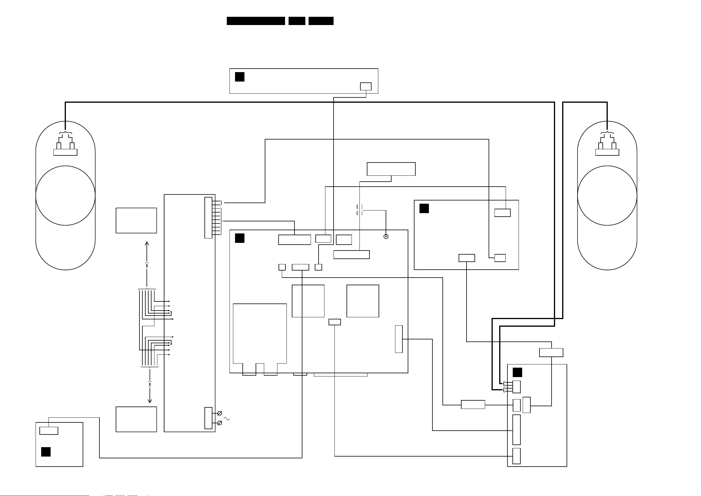
Wiring Diagram
TOP CONTROL
E
15LC4.1E AA 6.
1308
2P
LCD SCREEN
(LVDS) CONNECTION
TTL
Rigth
Speaker
BACK
LIGHT
CONNECTION
LCD SCREEN
INVERTER
1200
12P
SCALER
A
TUNER
1910 1206
12P
1007
1701
3P
7011 7401
5P
2P6P
1008
1402
1401
4P
1951
Left
Speaker
AUDIO AMPLIFIER
I
(5W)
5P
40P
1010
10P
1704
5P
1706
5P
1703
2P
FOR 2x5W
6P
1870
J
FRONT
IR/LED
BACK
LIGHT
CONNECTION
LCD SCREEN
POWER
IN
1001
FOR 2x2W
D
1110
SIDE I/O
1105
4P
1107
3P
5P
1108
10P
1111
4P
E_14520_001.eps
170904
Block Diagrams, Testpoint Overviews, and Waveforms
Block Diagram Audio & Video
16LC4.1E AA 6.
TUNER + VIF
A 3
A1
1302
TV
FM
SCL
A1
SDA
COMPAIR
1331
SSIF
A2
SEL_IF
A2
REAR IO SCART
A 3
A10
TER-Out
9
7
R-In
G-In
6
B-In
5
L-Out
2
R-Out
1
SIDE I/O (AV Part)
D
34
SVHS
2
1
7101
5
CVBS
L
R
SVHS
AUDIO IN
HERCULES (AUDIO)
A2
L/R_SC1_AV1_IN
AV3_LR_IN
PC_AUDIO_LR
SC1_LR_RF_OUT
+5VSW
6,7
4
2
1
3
SCART 1
21
20
1
Y/CVBS
A1
+VTUN
9
51
7316
CVBS-In
FBL-In
Status
L-In
R-In
2
C
L
R
SSIF(Tuner FM)
F306
11
10
F305
3311
10
1108 1010
4
2
6
7
9
10
7011 - SOUND
33
34,35
49,50
56,57
53,54
2321
6323
10
9
7
6
5
2
L
1
R
4
2
6
7
9
10
QSS/FM
3323
7320
7101
Audio Select
4327
4331
RF_AGC
4333
4334
+5VSW
EF
AD Conv
Std Stereo
Decoder
ADC/DAC
1328
2
3
1330
2
3
CVBS_SC1_AV1_IN
SC1 _CVBS_RF_OUT
AV3_C_IN
AV3_CVBS_Y_IN
I2S Proc
36,37
7
8
7
8
F312
VIF2
VIF1
F313
F314
SIF2
SIF1
F315
A2
73
Audio
Control
Vo l/T reb /
Bass
Featu res
DACs
70
HERCULES (IF+VIDEO)
A2
7011 - IF
25
24
31
30
29
CVBS_SC1_AV1_IN
AV3_CVBS_Y_IN
AV3 _C_ IN
SC1_CVBS_RF_OUT
SC1_FBL_IN
SC1_R_V_IN
SC1_G_Y_ IN
SC1_B_U_IN
LR_SC1_AV1_IN
SC1_L
AV3_LR_IN
PC_AUDIO_LR
61
60
62,63
OUT_MUTE
AGC
Detect
R_RF-OUT
AUDOUTLSR
AUDOUTLSL
Sound
Tr a p s
HERCULES 7011
TDA15001H
TDA15011H
TDA15021H
QSS Mixer/
AM Demod.
NAFTA
AP-NTSC / LATAM
EU / AP-PAL
A4
SOUND_ENABLE
POWER_DOWN
A2
EXT_MUTE
FROM 1,2-1200
INVERTER PANEL
CVBS1
CVBS/Y- X
QSS/FM
AM
C-X
55
58
51
59
52
43
64
AUDIO AMPLIFIER (2X2W)
(14, 15, and 17’’)
7702
7703
MUTE
MUTE
3
11
STANDBY
AUDOUT SL
AUDOUT SR
7703-1
MUTE
AUD_SUP
2718
2712
7710
AUDOUT SL
AUDOUT SR
A2
AUDOUT SL
AUDOUT SR
12
13
I
1
2
3
4
5
STANDBY
MUTE
7706
74LVCO8AD
1
&
2
&
AUDIO AMPLIFIER (2x5W) 20 & 23’’
1706
1703
Input
sw.
CS1A..D
Output
sw.
TDA1517ATW
I706
I707
7703-2
cvbs/y
INA..D
c
+
cvbs
A6
AUD_SUP
7712
3
18
17
MODE
OUT_MUTE
7709
TDA7297D
14
7
12
13
Dig. 2H/4H
Combfilter
Y Delay Adj.
Y_NOTCH
15,16
8,9
12,13
19 L+
16
2
5
H/V
I710
I711
A2
AUDOUT SL
AUDOUT SR
Y
int
Chroma
PA L / N T S C/
SECAM
Decoder &
Baseband
Delay
R/Pr-3
INSSW3
78
79 8077 74 75 76
5013
SECAM
only
2736
2737
STANDBY
MUTE
L-
R+
R-
U
int
V
int
RGB/YPRPB Insert
YUV Interface
G/Y3
B/Pb-3
1701
1
2
3
1706
1
2
3
4
5
1704
1
2
3
4
5
7014
EF
7012
2014
7005#
3005
6
THR
7
DISC
2015
RGB Matrix
Blue & Black
Stretch
Gamma Corr.
Skin Tone
U/V Tint
Saturation
YUV
Pea king
SCAVEM
U/V Delay
YUV IN/OUT
H/V
CON BRI
RGB Matrix
Blue & Black
Gamma Corr.
R_OSD
SAT
SCAVEM
on Text
Stretch
G_OSD
cvbs/y
Sync Sep
H-OSC
H-Shift
H-Drive
85
RO
GO
86
87
BO
B_OSD
Fast Blanking
F007
67
HOUT
FB/SC
66
7013
A3
SANDCASTLE
HISTOGRAM
7015
F006
7016
VSYNC
3031
1105
VDRA
23
VDRB
22
3010
4
3
2
1
R
4Ω/2W
OR
8Ω/5V
L
C-X
CVBS/Y-X
Vertical & EastWest Geometry
UIN
VIN
UOUT
YOU T
VOUT
2056
2027
YIN
70
71 72
2057
SIDE AV
D
(LS CONN. PART)
1110
1
2
3
1106
HEADPHONE
1107
1
2
3
4
5
OR
OR
VCC
CTRL
8
5
EF
EF
TR
RES
OUT
2028
2040
3036
2042
I044
I041
I039
2
4
3
7007#
6
7
R_SDTV
G_SDTV
B_SDTV
+5VSW
7006#
3025
6
THR
7
DISC
2029
# = NE555 TIMER
8
VCC
THR
TR
RES
DISC
OUT
CTRL
5
2045
VCC
CTRL
2
4
3
8
TR
RES
OUT
5
2034
+5VSW
TO
A8
SEE
BLOCKDIAGRAM
SCALER
2
4
H_CS_SDTV
3
A8
V_SDTV
A8
E_14520_002.eps
170904
Block Diagrams, Testpoint Overviews, and Waveforms
Block Diagram Scaler & Supply
17LC4.1E AA 6.
A8
1
2
15
3
1511
9
12
13
14
15
TOP CONTROL
E
5x
CHANNEL +
CHANNELVOLUME+
VOLUMEPOWER
FRONT IR/LED
J
+3V3STBY
HERCULES (CONTROL)
A2
KEYBOARD
IR
STATU S_1
A8
P50_LINE_ITV_IR_SW
A3
+1V8_A
+1V8_B
HERC_RESET
DECDIG
+3V3STBY
+5VSW
HERCULES (SUPPLY)
A3
7001,7003
+3V3STBY
DECDIG
HERC_RESET
PCHD-IO
RED_PR
GREEN_Y
BLUE_PB
VGA_5V
SDA
HS
VS
SCL
KEYBOARD
7802
RC
RECEIVER
3802
7801
6801
7070
1308
2
1
7803
REDGREEN
7804
120
115
119
116
123
3,93,96
100,117,118,124
127
4,5,7,9,88,90,94
15,69,82
F014
F015
7011
97
P1.4
DECDIG
14
+1V8_A
+1V8_B
DCC_VGA_5V
LED_SEL
+3V3STBY
PC_TV_LED
u-Processor
HERCULES
IC
N.C.
IR
114
111
107
108
109
104
102
99
98
122
126
128
10
11
+5VSW
6460
7462
1870
1
2
3
4
5
6
SOUND_ENABLE
NVM_WP
6073
6076
1001
VGA_5V
6
8
DDC
NVM
A3
1008
1007
SDM PINS
4015
SEL_IF
PC-TV-LED
SCL
SDA
56
7099
7
NV
2k x 8
EXT_MUTE
TV_SC_COM
TV_IRQ
STANDBY
POWER_DOWN
2007
2006
PC_DET
3470
5
HERCULES
(FRONT CONTROL LOOP THROUGH)
2
KEYBOARD
1
2
3
4
5
6
M
A7
KEYBOARD
IR
LED_SEL
+3V3STBY
PC_TV_LED
A1
A3
A1
A7
A5
A3
A5
A4
A5
FROM
SUPPLY
PAN E L
1910
1
2
3
4
5
6
7
8
9
10
11
12
A5
A3
A4
+5VSW+3V3STBY
60603062
7060
A2
UART
CONN.
FOR
SERVICE
TV-SUPPLY
F903
F905
F906
F907
POWER_DOWN
BACK_LIGHT_ADJ1
LAMP_ON_OFF
D
1112
1
2
3
AUD_SUP
+3V3STBY
+3V3STBY
+12VSW
STANDBY
FROM
A2
see
blockdiagram
VIDEO
A7
A3
A7
A3
A7
A2
SIDE AV
(UART PART)
3123
3124
3931
5930
A2
A3
A4
A2
A7
A7
R_SDTV
G_SDTV
B_SDTV
RED_PR
GREEN_Y
BLU_PB
HD_FILTER
SD_PCHD_SEL
PC_HD_SEL
H_CS_SDTV
V_SDTV
HS
VS
SD_PCHD_SEL
H_CS_SDTV
PLL_SEL
Y_NOTCH
+3V3STBY
7930
8
7
OSC
VCC
6
5920
13
13
1
12
2
7920
7463
10,11
SCALER (ANA IN)
A6
7401
GM5221
7461
27
3
17
7
25
1
5
21
22
R_PR+
14
G_Y+
11
B_PB+
23
3497
3499
3479
2466
2468
2470
SOG
R_PR-
G_Y-
B_PB-
ANALOG
INPUT
PORT
+
TRIPLE
ADC
&
PLL
7510
23 4
14
1
15
69 8
5
1111
1
2
3
4
3937
1
Q
S
R
5
2
3
4
REF
2
2931
3910
7910
2921
7520
MK1575-01
RECOVERY
1401
1
2
3
4
3936
5931
5910
CLOCK
PLL
5932
CS_HSYNC
VSYNC
69
F913
F911
6910
F912
12
2
+3V3STBY
7936
30
6911
F499
F503
PLL_SEL
+5
VSW
+VTUN
+8VSW_TV
A7
A9
Y_NOTCH
7403
M29W040B-55k1
FLASH
ROM
512kx8
7402
M24C32
EEPROM
(NVM)
4kx8
SDA
A2
JTAG_SDL_UART_TX
JTAG_SCL_UART_RX
SCL
SUPPLY
+3V3STBY
32
FBINFBIN
7955
N.C.
DATA
ADDRESS
1403
14M31818
SDA_IO
SCL_IO
3430
3431
3442
3441
1
169
170
WC
F954
2997
DVI
INPUT
VIDEO
ROM
INTERFACE
CLK_SYN
SYSTEM
+1V8
SCALER (LVDS, TTL OUT)
A7
LV DS
Tx
22
21
20
19
18
17
14
13
16
15
38
37
36
35
34
33
32
31
30
29
43
44
45
46
47
48
49
55
67
68
81
82
83
85
88
90
98
100
101
LV_E0_TX0-
LV_E1_TX0+
LV_E2_TX1-
LV_E3_TX1+
LV_E4_TX2-
LV_E5_TX2+
LV_E8_TX3-
LV_E9_TX3+
LV_E6_TXC-
LV_E7_TXC+
LV_ O 0
LV_ O 1
LV_ O 2
LV_ O 3
LV_ O 4
LV_ O 5
LV_ O 6
LV_ O 7
LV_ O 8
LV_ O 9
PD20
PD21
PD22
PD23
FED
FHSYNC
FVSYNC
FSHCLK
PANEL_PWR_CTL
LAMP_ON_OFF
TV_SC_COM
TV_IRQ
FBIN
PC_DET
SD_PCHD_SEL
POWER_DOWN
7437
BACK_LIGHT_ADJ1
PLL_SEL
BACK_LIGHT_ADJ2
PAN_VCC
EG1
EG0
ER7
ER6
ER5
ER4
ER1
ER0
ER3
ER2
EB3
EB2
EB1
EB0
EG7
EG6
EG5
EG4
EG3
EG2
EB4
EB5
EB6
EB7
A9
A5
A2
A2
A6
A8
A8
A2
A8
F534
LV_E0_TX0-
LV_E1_TX0+
LV_E2_TX1-
LV_E3_TX1+
LV_E4_TX2-
LV_E5_TX2+
LV_E6_TX3-
LV_E7_TX3+
LV_E8_TXC-
LV_E9_TXC+
FED
FHSYNC
FVSYNC
FSSYNC
PAN_VCC
A8
A3
A5
1404
1
2
3
4
6
8
10
12
18
20
14
16
1402
1
17
19
21
23
24x
25
27
29
31
33
35
37
39
42
38,36
A5
A5
E_14520_033.eps
230904
To LCD MONITOR (LVDS)
(MAINLY FOR 20”)
To LCD MONITOR (TTL)
Block Diagrams, Testpoint Overviews, and Waveforms
Testpoint Overview TV & Scaler Board (Top Side)
18LC4.1E AA 6.
I413 A4
X1
SERVICE TESTPOINT
I414 B4
I415 A4
I416 B4
I417 A4
I418 B4
I419 A5
I420 B4
I421 A5
I422 B4
I424 B5
I425 A5
I426 B5
I427 A5
I428 B5
I429 A4
I430 B5
I431 A4
I432 B5
I434 B5
I436 B5
I437 A5
I438 B5
I439 A5
I440 B5
I441 A5
I442 B5
I443 A5
I444 B5
I445 A5
I446 B5
I447 A5
I448 B5
I449 A5
I450 B5
I451 A5
I452 B5
X1
X1
500mV / div DC
5ms / div
3139 123 5833.3
E_14520_005.eps
160904
 Loading...